Article

Reducing Circling Currents in a VHF Class Φ2 Inverter Based on a Fully Analytical Loss Model

1
School of Optical and Electronic Information, Huazhong University of Science and Technology, Wuhan 430074, China
2
Beijing Institute of Spacecraft System Engineering, Beijing 100094, China
3
School of Automation, Wuhan University of Technology, Wuhan 430070, China
*
Author to whom correspondence should be addressed.
Energies 2022, 15(22), 8572; https://doi.org/10.3390/en15228572
Submission received: 18 October 2022 / Revised: 8 November 2022 / Accepted: 14 November 2022 / Published: 16 November 2022
(This article belongs to the Special Issue High-Performance Power Converters and Inverters)

Abstract

:
This paper proposes a fully analytical loss model to reduce circling currents and improve the power efficiency of a class Φ2 inverter. Firstly, analytical expression of the switching node voltage is derived by analyzing its harmonic components. Based on the result, the power switch is modeled as a voltage source, where the circuit is simplified to a linear network and analytical expressions of branch currents are solved. Secondly, root mean square (RMS) values of branch currents and component losses are calculated to form the analytical loss model for a Φ2 inverter. The influence of circuit parameters on the circling current and power efficiency are thoroughly analyzed, which derives optimal design constraints to reduce circling currents of a class Φ2 inverter. Furthermore, detailed design guidance and equations are provided to calculate circuit parameters of a class Φ2 inverter, which reduces its circling currents and improves overall power efficiency. Finally, a class Φ2 inverter prototype is built, and experimental results demonstrate a 7% efficiency improvement compared to conventional empirical design methods.

1. Introduction

Increasing the operation frequency can reduce the values of inductors and capacitors while maintaining the same voltage and current waveforms. Thus, the energy storage and volume of passive components (inductors and capacitors) are reduced, which provides great potential for a high power density and a fast dynamic response [1,2,3,4]. However, the switching losses increase greatly with the increase of switching frequency, which degrades the overall power efficiency. To maintain a high efficiency while increasing the operating frequency, it is essential to realize zero-voltage-switching (ZVS) and zero-current-switching (ZCS) for VHF power systems [5,6,7]. Owing to the easy realization of ZVS, low switch voltage stress and ground-referenced switch, class Φ2 topology is widely used not only in DC–DC converters [8,9,10,11] and wireless power transfer systems [12,13,14,15], but also as power amplifiers in plasma generation [16,17] and medical imaging [18].
The topology of a class Φ2 inverter is shown in Figure 1, which consists of a resonant tank, a power switch and an output network. Compared to class E topology, the class Φ2 inverter adds a second harmonic resonant branch across the power switch, i.e., LM-CM in Figure 1. By absorbing the second harmonic voltage, the class Φ2 inverter significantly reduces the switch voltage stress from 3.6–4 vin to 2–2.4 vin. Parameters of the resonant tank directly affect the inverter performance, such as power efficiency and switch voltage stress. To improve its performance, extensive research has been carried out on the modeling and design of VHF class Φ2 inverters [19,20,21,22]. The conventional empirical design method usually chooses the value of the resonant capacitor CF based on the designers’ experience [23], and values of other parameters are roughly calculated according to pole and zero positions of the resonant tank. Then, further iterative simulations are required to improve the circuit performance. The conventional empirical design method highly relies on experience, and improper selections for CF would result in high voltage stress or low power efficiency. The parameter scanning method can reduce power switch voltage with massive computer aided simulations [24]. However, circling losses are not considered, and it is hard to reduce switch voltage stress and improve power efficiency simultaneously.
To provide detailed guidance for the resonant parameters design of class Φ2 inverters, extensive research has been carried to explore modeling methods for class Φ2 inverter. To minimize resonant current magnitude and conduction losses for resonant power converters, an analytical switching cell model is proposed based on the fundamental harmonic approximation (FHA) [25]. However, the third harmonic is neglected in [25], which induces a large error for class Φ2 inverters. A study [26] established a mathematical model by solving differential equations of the class Φ2 inverter, where the high-order resonant tank is approximated by a capacitor with an equivalent series resistor (ESR). The approximation simplifies the calculations but induces a larger error for the Φ2 inverter. To improve the model accuracy and achieve maximum output capacity, a normalized full-order model is proposed which considers high-order voltage and current harmonics [27]. However, the above methods have not explored the relationship between resonant parameters and the power efficiency. To realize optimal parameter design and reduce circling losses of class Φ2 inverters, an accurate model considering inductor ESR is required to perform fully quantitative calculations.
To achieve efficiency optimization for class Φ2 inverters, this paper proposes an analytical loss model for class Φ2 inverters based on harmonic analysis. Firstly, harmonic magnitudes of the switching node voltage are thoroughly analyzed based on operating principles of class Φ2 inverters. With the results, the power switch is modeled as a voltage source, which simplifies the inverter as a linear network and derives analytical expressions of branch currents. Secondly, root mean square (RMS) values of branch currents and component losses are calculated to establish the analytical loss model. Furthermore, the relationship between the circuit parameters and the overall power efficiency are thoroughly explored. Detailed parameter design guidance and equations are provided to reduce circling losses and improve power efficiency of class Φ2 inverters. Finally, a class Φ2 inverter prototype is built to verify the effectiveness of the proposed design strategy.
The rest of this paper is organized as follows. Section 2 describes operating principles of class Φ2 inverters. In Section 3, the analytical loss model for a class Φ2 inverter is presented. Based on the model, detailed design guidance for resonant parameters is provided to reduce the circling loss of class Φ2 inverters. Section 4 and Section 5 presents simulation and experimental results, respectively. Section 6 concludes this paper.

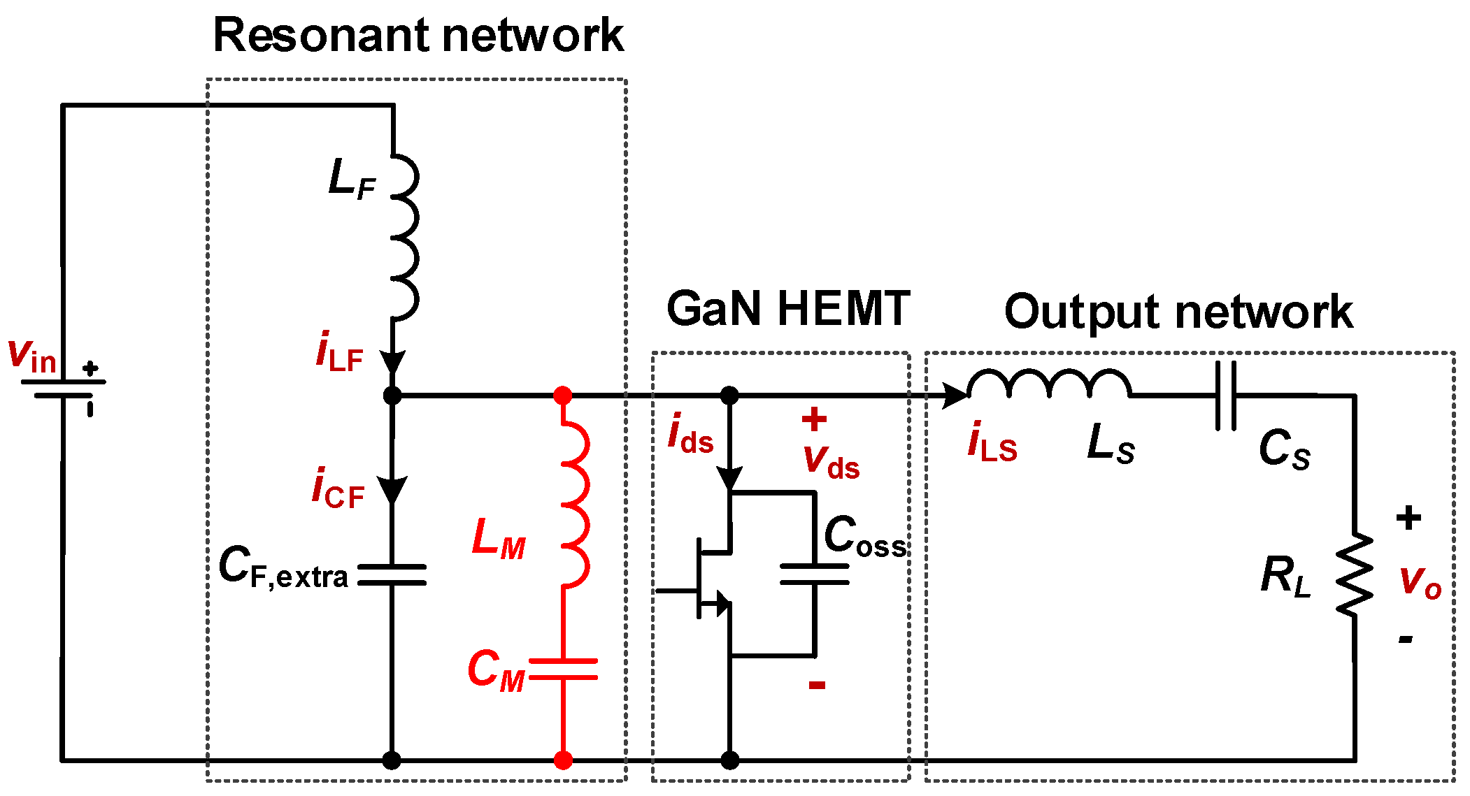
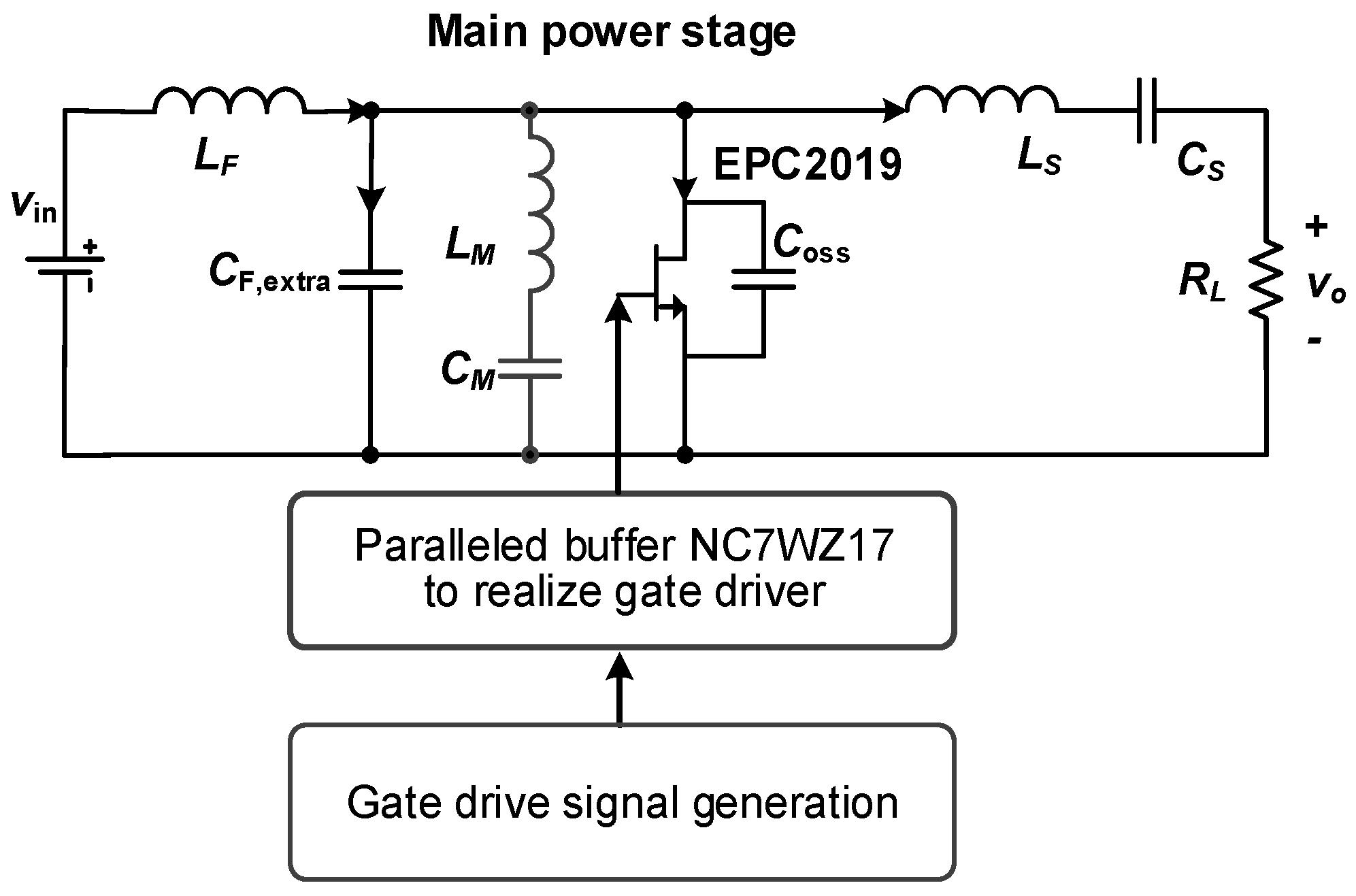
2. Topology and Operating Principles of a Class Φ2 Inverter

The topology of a class Φ2 inverter consists of a resonant tank, a power switch and a load network, as shown in Figure 1. Compared to a class E inverter, a class Φ2 inverter adds a second harmonic resonant branch, i.e., LM and CM, to reduce the switch voltage stress. LF, CF, LM and CM form a high-order resonant tank, which shapes the switching node voltage. Voltage waveforms with different harmonics are shown in Figure 2. Figure 2a shows the switching node voltage consisting of fundamental and third harmonics, while Figure 2b shows the switching node voltage consisting of fundamental and second harmonics. It shows that the third harmonic can effectively reduce the peak value of the switching node voltage.
By properly designing pole and zero positions of the resonant tank, the switching node voltage is formed by the fundamental and third harmonics, which reduces it peak value. Specifically, the switching node impedance consists of two pairs of conjugation poles and a pair of conjugation zeros. Two conjugation poles of the resonant tank are placed at ωs and 3ωs, while the conjugation zeros are placed at 2ωs, where ωs = 2πfs and fs is the operating frequency of the class Φ2 inverter. With the above settings, the switching node impedance is high at ωs and 3ωs, whereas the switching node impedance is low at 2ωs. Therefore, the switching node voltage is formed by fundamental and third harmonics, where the second harmonic is absorbed owing to the zeros at 2ωs.
Based on the above analysis, conventional design methods set the poles at ωs and 3ωs, and the zeros at 2ωs. Thus, the resonant parameters should satisfy Equation (1) [23].
L F = 1 9 π 2 f s 2 C F , L M = 1 15 π 2 f s 2 C F , C M = 15 16 C F
There are four parameters LF, CF, LM, CM, but only three equations are provided. Thus, with conventional design methods, designers are required to choose the value of CF according to the rated output power and the designers’ experience. Then, values of other parameters are calculated by Equation (1). Furthermore, a time-consuming iterative parameter tuning procedure based on circuit simulations is required to adjust values of LF and CF, to achieve the desired switch voltage shape. Typically, CF is increased to reduce switch voltage stress and LF is reduced to ensure ZVS. The step-by-step design procedure can be found in [23].
Since conventional design methods do not perform fully quantitative calculations, it is hard to achieve an optimal design for a class Φ2 inverter. Specifically, the selection of CF highly relies on experience. A small value for CF can reduce circling loss, but it will lead to an insufficient power transfer capacity and a large switch voltage stress. A large value for CF can reduce the switch stress, but it increases circling losses which degrades the overall power efficiency. Without fully quantitative calculations, the power efficiency of the Φ2 inverter is hard to optimize.

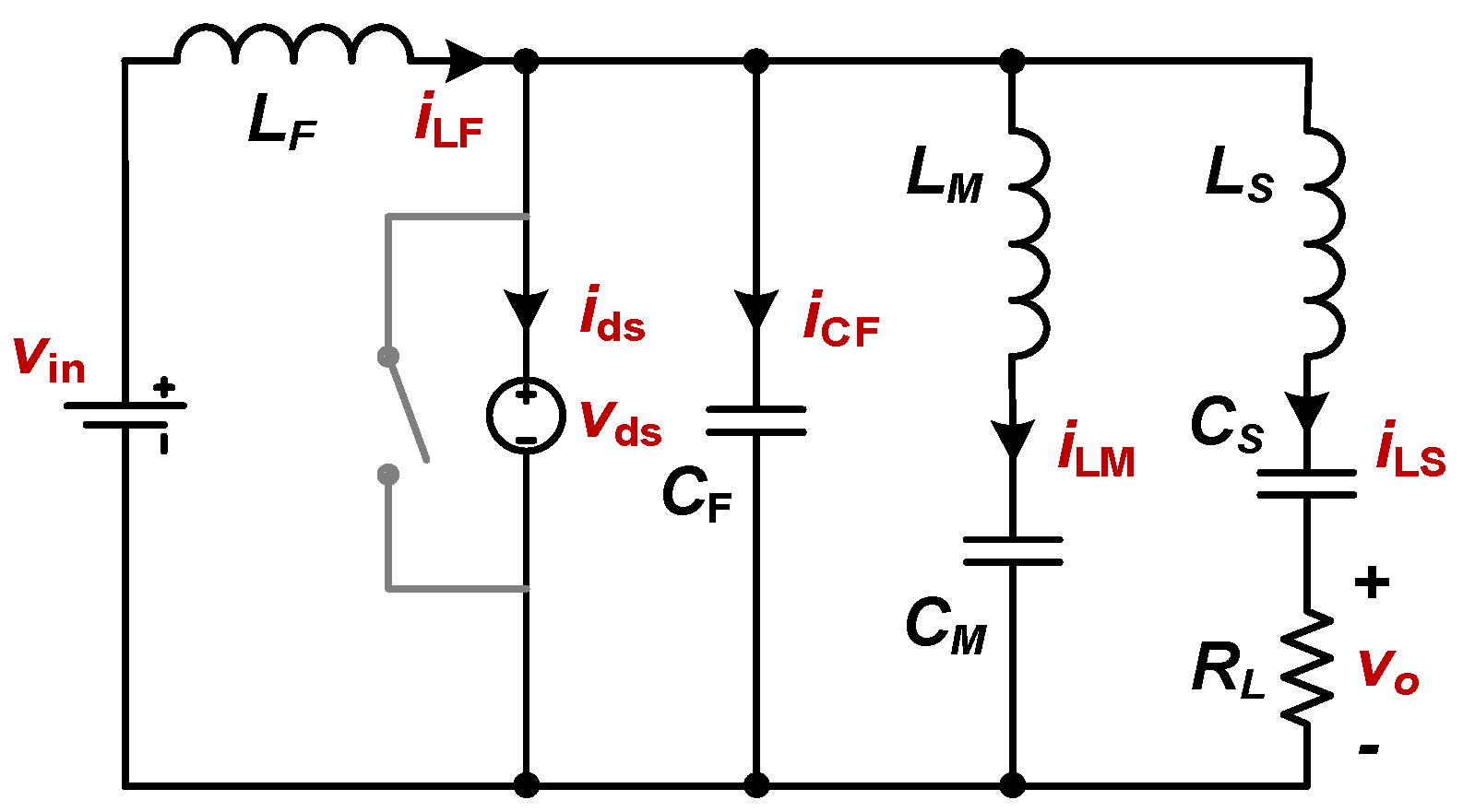
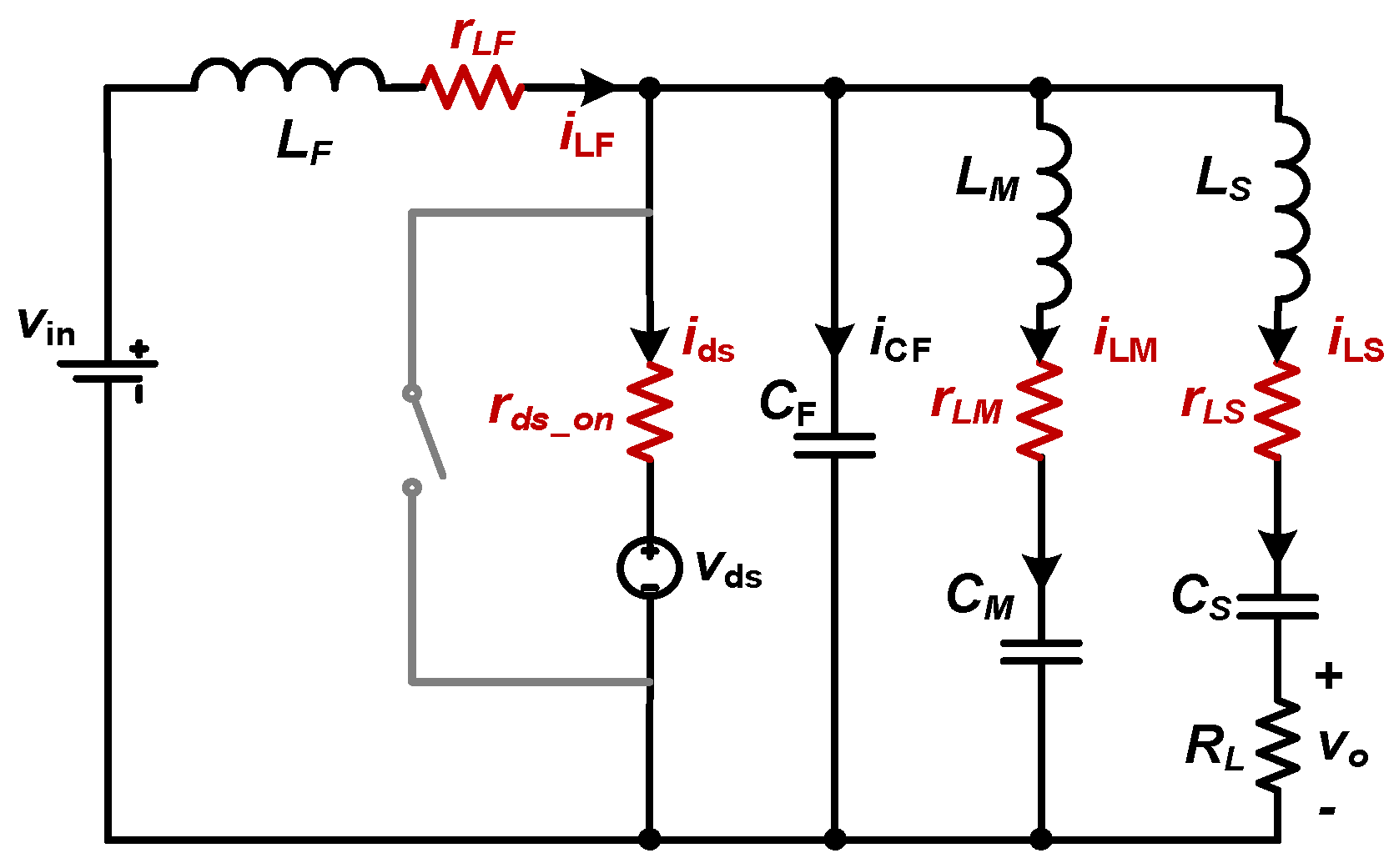
3. Analytical Loss Model for a Class Φ2 Inverter

To provide a fully quantitative theoretical analysis and improve the power efficiency of class Φ2 inverters, this paper proposes an analytical loss model based on voltage and current harmonic analysis. Firstly, based on basic principles of class Φ2 inverters, harmonic components and an analytical expression of switching node voltage are derived. With the results, the power switch is modeled as a voltage source to simplify the calculations. Then, analytical expressions and RMS values of branch currents are calculated based on the switching node voltage, which forms the analytical loss model of class Φ2 inverters. Furthermore, the influence of resonant parameters on the total loss and power efficiency are thoroughly analyzed, and detailed design guidance and equations for class Φ2 inverters are provided.

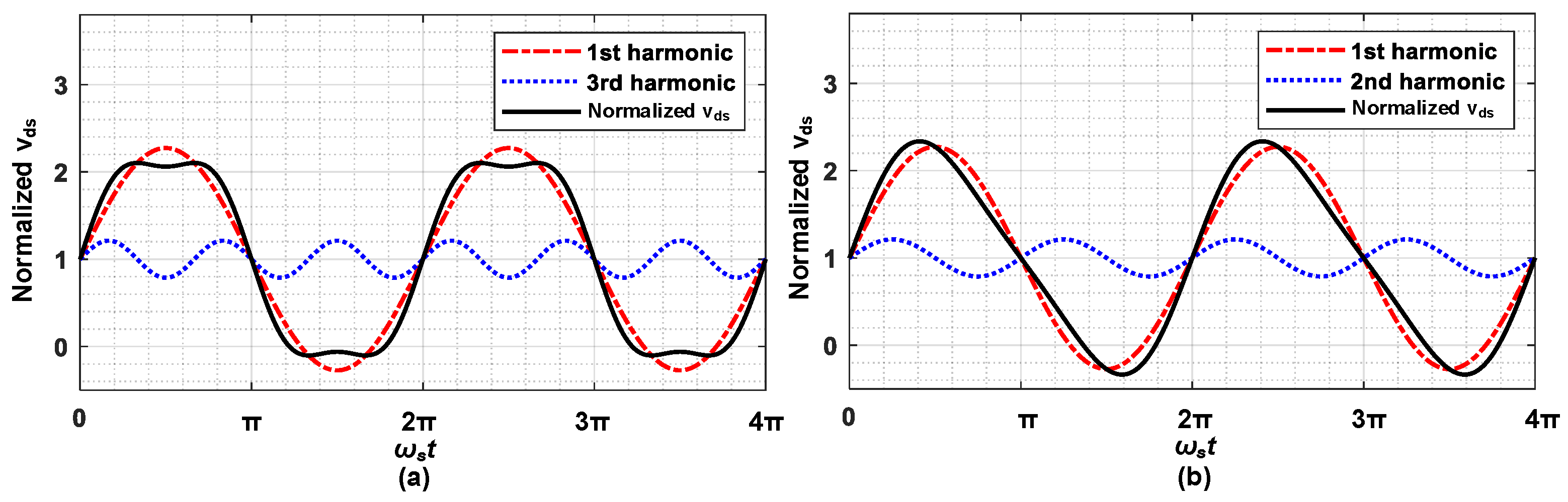
3.1. Switching Node Voltage and Branch Currents Analysis

Based on the principles of class Φ2 inverters, the switching node voltage mainly consists of the fundamental and the third harmonic. To reduce the switch voltage stress, the fundamental and third harmonics should remain in phase. Additionally, the DC component of the switching node voltage (vds) equals the input voltage vin, which is derived according to the voltage-second balance of LF. Therefore, the analytical expression of vds is given by
v d s ( t ) = v i n + v 1 sin ( ω s t ) + v 3 sin ( 3 ω s t )
where v1 and v3 are the magnitudes of the fundamental and the third harmonic, respectively. To minimize the switch voltage stress, v1 and v3 are 4 vin/π and 2 vin/3π, respectively. With the analytical expressions of vds(t), the power switch is modeled as a voltage source to simplify the calculations. The equivalent circuit is shown in Figure 3.
Based on Figure 3, branch currents in a class Φ2 inverter are calculated as follows. The current of LF is calculated by integrating the voltage across it, i.e.,
i L F ( t ) = 1 L F 0 t v i n v d s ( t ) d t = v 1 cos ( ω s t ) ω s L F + v 3 cos ( 3 ω s t ) 3 ω s L F + i ¯ d s = 4 v i n cos ( ω s t ) π ω s L F + 2 v i n cos ( 3 ω s t ) 9 π ω s L F + i ¯ d s
where i ¯ d s the is average value of the power switch current, calculated using the load power and input voltage. The current of CF is calculated by differentiating the voltage across it, i.e.,
i C F ( t ) = C F d v C F ( t ) d t = v 1 ω s C F cos ( ω s t ) + 3 v 3 ω s C F cos ( 3 ω s t ) = 4 v i n ω s C F cos ( ω s t ) π + 2 v i n ω s C F cos ( 3 ω s t ) π
Furthermore, by dividing the switching node voltage with the impedance of the load network, the current of LS is calculated as
i L S ( t ) = v 1 | Z L ( j ω s ) | sin ( ω s t Z L ( j ω s ) ) + v 3 | Z L ( j 3 ω s ) | sin ( 3 ω s t Z L ( j 3 ω s ) ) = 4 v i n π | Z L ( j ω s ) | sin ( ω s t Z L ( j ω s ) ) + 2 v i n 3 π | Z L ( j 3 ω s ) | sin ( 3 ω s t Z L ( j 3 ω s ) )
ZL(s) is impedance of the load network, which is given by
Z L ( j ω s ) = R L + j ω s L S + 1 j ω s C S R L + j ω s L S
where CS is a DC-blocking capacitor and is near-shorted at the switching frequency. The value of LS is calculated according to required output power.
Furthermore, the current of LM is calculated as follows. When the power switch is on, the LM-CM branch satisfies the zero-input response equation, since it is a source-free resonant circuit during this period.
{ L M d i L M ( t ) d t + v C M ( t ) = 0 i L M ( t ) = C M d v C M ( t ) d t
The analytical expression of iLM(t) is derived by solving (7), which is given by
i L M ( t ) = I 2 sin ( 1 L M C M t )
where I2 is the magnitude of the current in LM-CM and it is determined by the energy stored in LM and CM at the switching-off moment. When the power switch is off, the power switch current is zero. Thus, when the power switch is off, the current of LM is calculated as
i L M ( t ) = i L F ( t ) i C F ( t ) i L S ( t )
In this paper, I2 is approximated as the maximum value of (9) which has been verified by the LTspice simulation. The SPICE netlist for the LTspice simulation is provided in Appendix A. In fact, with proper design to reduce losses of the class Φ2 inverter, the resonant switching frequency of LM-CM is 2ωs and current of LM-CM only contain the second harmonic. Therefore, (8) can represent the current of LM-CM in a whole switching period, i.e.,
i L M ( t ) = I 2 sin ( 2 ω s t )
Furthermore, the current of the power switch is calculated as
i d s ( t ) = i L F ( t ) i L M ( t ) i C F ( t ) i L S ( t ) = 4 v in π ω s L F cos ( ω s t ) + 2 v in 9 π ω s L F cos ( 3 ω s t ) + i d s ¯ I 2 sin ( 2 ω s t ) 4 v in C F ω s π cos ( ω s t ) 2 v in C F ω s π cos ( 3 ω s t ) 4 v in sin ( ω s t Z L ( j ω s ) ) π | Z L ( j ω s ) | 2 v in sin ( 3 ω s t Z L ( j 3 ω s ) ) 3 π | Z L ( j ω s ) | i d s ¯ + I 1 sin ( ω s t + θ 1 ) I 2 sin ( 2 ω s t ) I 3 sin ( 3 ω s t + θ 3 )
where I1, I3 θ1 and θ3 are given by
{ I 1 = 4 v in π ( 1 ω s L F C F ω s + 1 | Z L ( j ω s ) | sin ( Z L ( j ω s ) ) ) 2 + ( cos ( Z L ( j ω s ) ) | Z L ( j ω s ) | ) 2 I 3 = 2 v in 3 π ( 1 3 ω s L F 3 C F ω s + 1 | Z L ( j 3 ω s ) | sin ( Z L ( j 3 ω s ) ) ) 2 + ( cos ( Z L ( j 3 ω s ) ) | Z L ( j 3 ω s ) | ) 2 θ 1 = asin [ cos ( Z L ( j ω s ) ) ] = π 2 Z L ( j ω s ) θ 3 = asin [ cos ( Z L ( j 3 ω s ) ) ] = π 2 Z L ( j 3 ω s )
With the above calculations, analytical expressions of branch currents are derived. Based on the results, component losses are calculated to establish the analytical loss model for a class Φ2 inverter.

3.2. Analytical Loss Model for a Class Φ2 Inverter

Losses of power converter mainly include conduction losses and switching losses. In class Φ2 inverters, the turning-on loss of the power switch is eliminated owing to zero-voltage switching (ZVS). Additionally, the use of a gallium nitride high electronic mobility transistor (GaN HEMT) greatly reduces the turning-off loss of power switch. Therefore, in a class Φ2 inverter, the losses are mainly caused by a parasitic resistance of inductors and the on-resistance of the GaN HEMT. A circuit model considering inductor parasitic resistance and power switch on-resistance is shown in Figure 4.
Based on the derived branch currents in Section 3.2, losses of the inductors and the power switch are calculated to established the loss model for a class Φ2 inverter.
Conduction loss of LF is given by
P L o s s _ L F = r L F T 0 T i L F 2 ( t ) d t
Substituting (3) to (13) yields
P L o s s _ L F = r L F ( i ¯ 2 d s + 1 2 ( 4 v i n π ω s L F ) 2 + 1 2 ( 2 v i n 9 π ω s L F ) 2 )
Similarly, the conduction loss of LM is calculated as
P L o s s _ L M = r L M T 0 T i L M 2 ( t ) d t = r L M I 2 2 2
The conduction loss of LS is calculated as
P L o s s _ L S = r L S T 0 T i L S 2 ( t ) d t = r L S ( 1 2 ( 4 v i n π Z L ( j ω s ) ) 2 + 1 2 ( 2 v i n 3 π Z L ( j ω s ) ) 2 )
The conduction loss of the power switch is calculated as
P L o s s _ S W = r d s , o n T 0 T i d s 2 ( t ) d t = r d s , o n ( i ¯ d s 2 + I 1 2 2 + I 2 2 2 + I 3 2 2 )
Therefore, the total loss of a class Φ2 inverter is calculated as
P L o s s = P L o s s _ L F + P L o s s _ L M + P L o s s _ L S + P L o s s _ S W
Furthermore, the output power of a class Φ2 inverter is calculated as
P o = R L ( 1 2 ( 4 v i n π Z L ( j ω s ) ) 2 + 1 2 ( 2 v i n 3 π Z L ( j ω s ) ) 2 )
The overall power efficiency of a class Φ2 inverter is calculated as
η = P O P O + P L o s s

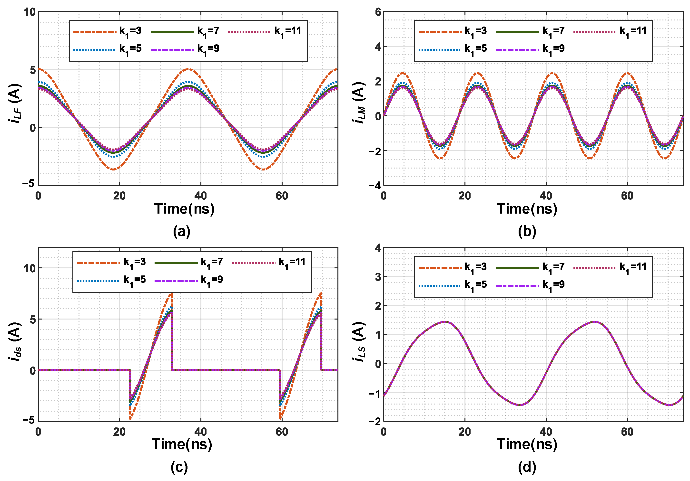
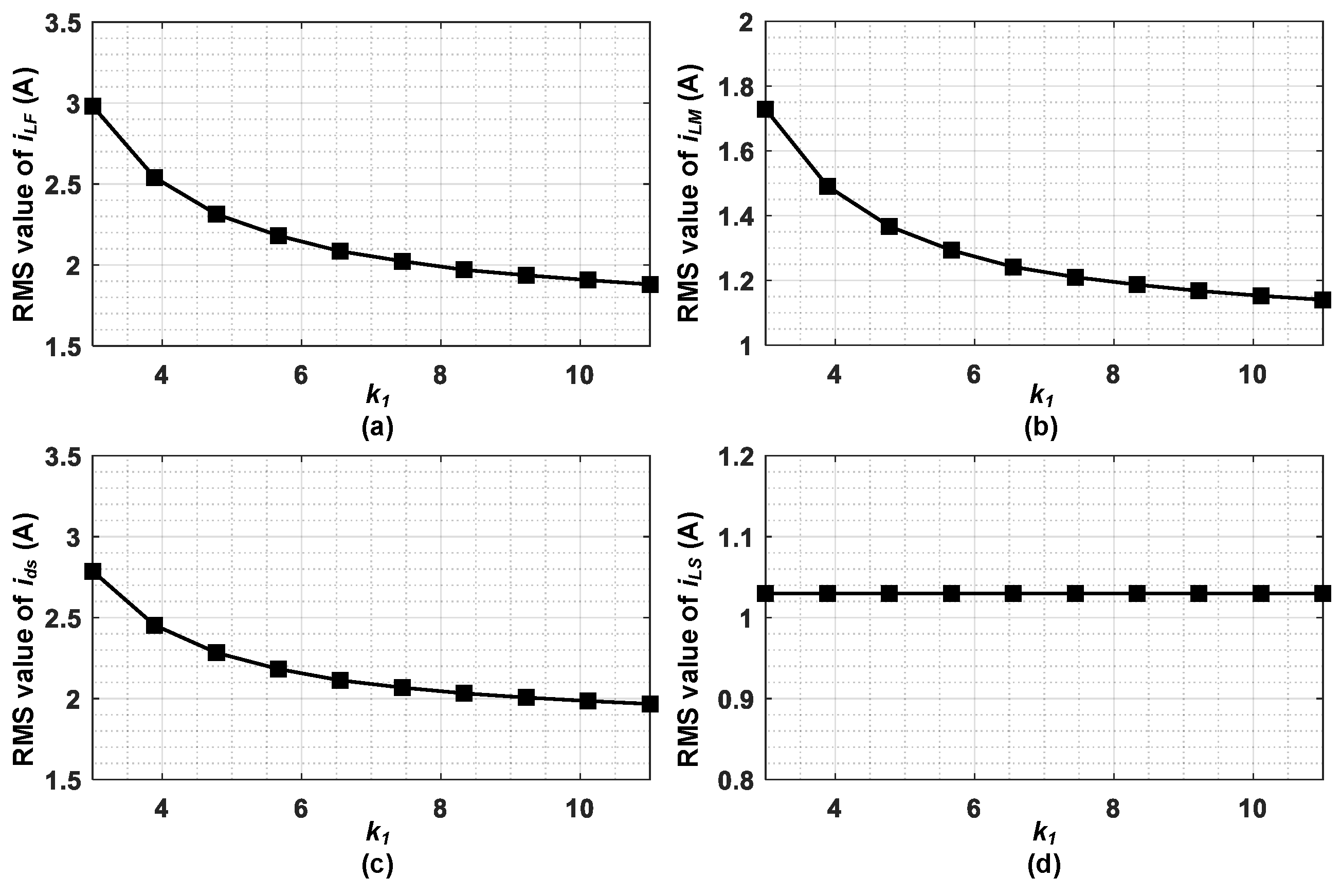
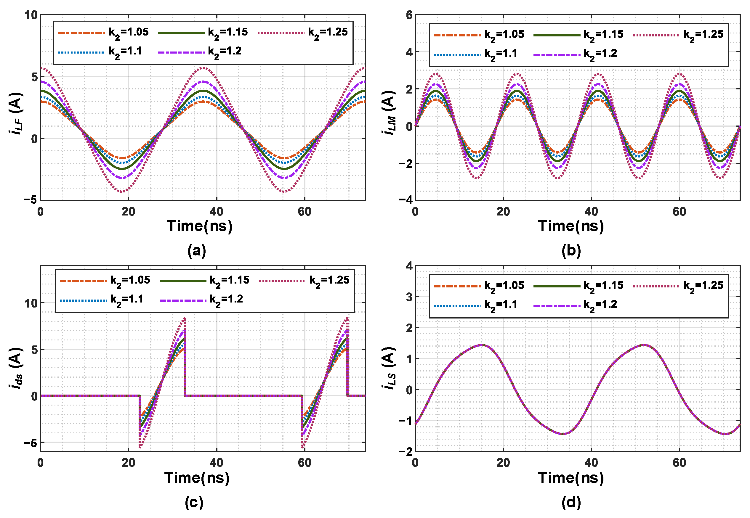
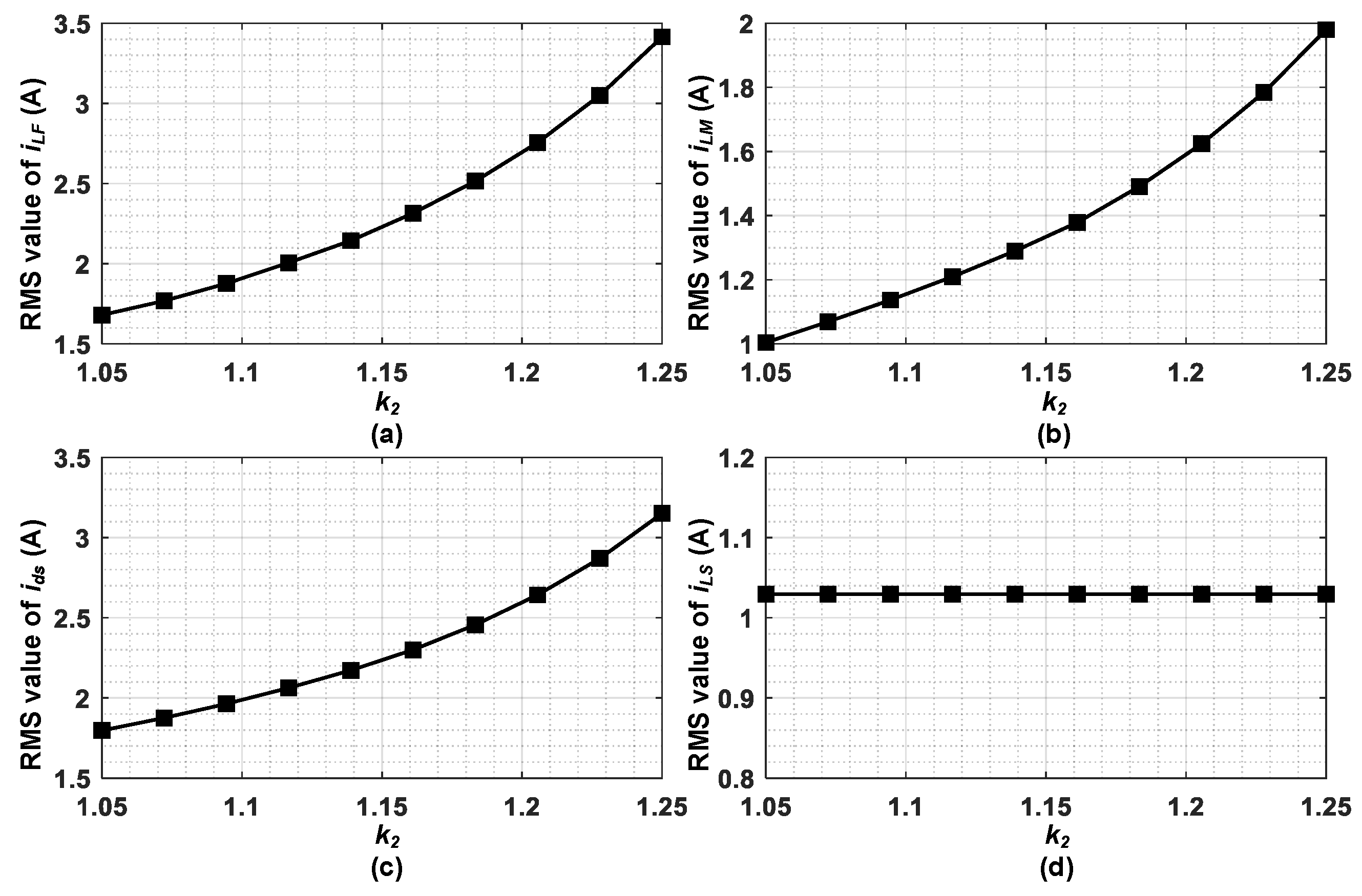
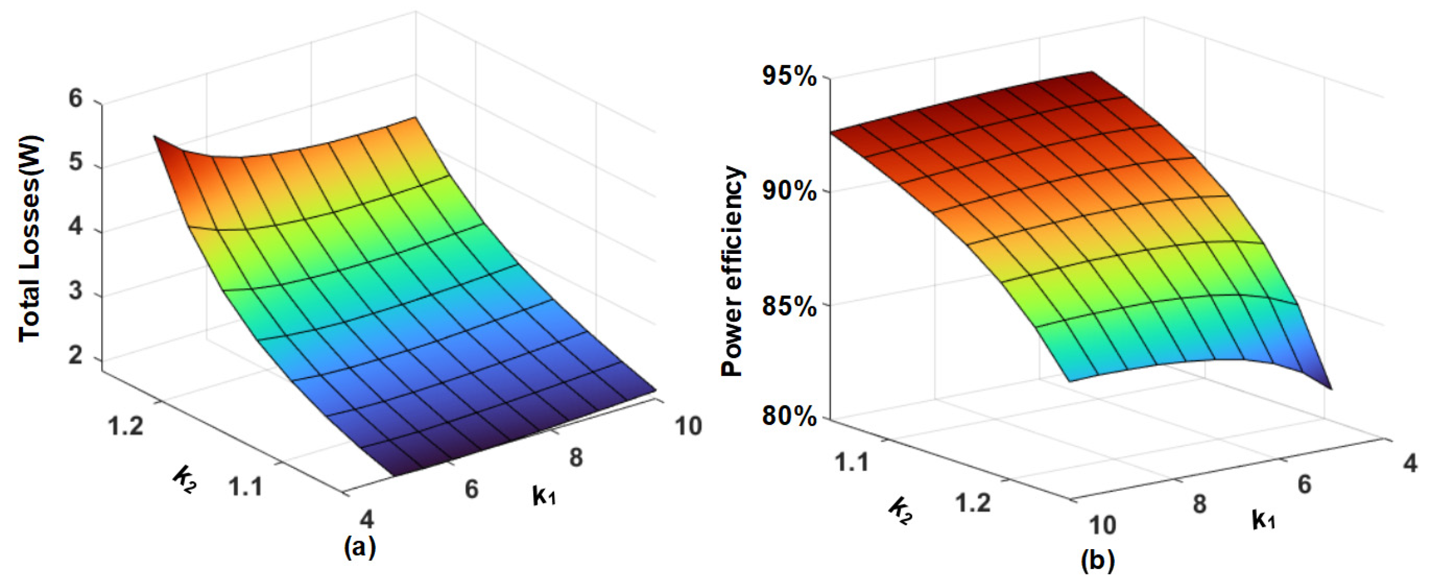
3.3. Design Guidance to Reduce Total Loss

In Section 3.2, an analytical loss model for a class Φ2 inverter is established. To achieve efficiency optimization, this section thoroughly explores the influence of circuit parameters on the total loss of a class Φ2 inverter. Detailed design guidance is provided to reduce circling losses and improve overall power efficiency.
Conventional design methods derive constraints on-resonance parameters from an empirical perspective. The impedance of the resonant tank is given by
Z M R ( j ω ) = j ω L F ( 1 ω 2 L M C M ) 1 ω 2 ( L M C M + L F C F + L F C M ) + ω 4 L M C M L F C F
Observing (21), it is found that ZMR() consists of two pairs of conjugation poles (P1,2, P3,4) and a pair of conjugation zeros (Z1,2). Then, based on principles and physical intuition for class Φ2 inverters, conventional design methods set P1,2 = ωs, P3,4 = 3ωs and Z1,2 = 2ωs. However, there are four parameters, but only three equations are provided. Designers must select a value for the resonant element, which highly relies on experience. Moreover, the constraints P1,2 = ωs and P3,4 = 3ωs are derived by qualitatively analyzing operation principles of class Φ2 inverters. Therefore, it is hard to realize optimal design, such as minimized voltage stress, minimized circling losses and maximum power efficiency. In this section, design constraints are reconsidered to realize efficiency optimization while minimizing switch voltage stress.
In fact, Z1,2 = 2ωs is the optimal setting to absorb the second harmonic of the switching node voltage, to reduce the peak value of the switching node voltage. Furthermore, to minimize the switch voltage stress, the switching node impedance should satisfy
Z d s ( j ω s ) Z d s ( j 3 ω s ) = 6 I 3 I 1
where Zds(s) = ZMR(s) || ZL(s), and I1 and I3 are magnitudes of the switch current at ωs and 3ωs, respectively.
The above constraints can realize the optimal design of the power switch voltage stress. To reduce the circling losses, further analyses are carried out as follows. Firstly, the LM-CM branch is designed to absorb the second harmonic voltage. At ωs and 3ωs, the magnitude of the LM-CM series resonant branch should be large, to reduce the fundamental and third harmonic currents in LM. The small capacitor and large inductor form a high characteristic impedance, which reduces unnecessary circling losses. Therefore, the ratio of CM and CF is selected as a design constraint to represent circling loss in the LM-CM branch, i.e.,
k 1 = C F C M
where k1 is larger than 1.
Additionally, to guarantee zero-voltage switching (ZVS) of the power switch, Zds(s) must be inductive at ωs. Therefore, the lower poles (P1,2) of ZMR(s) need to be located between ωs and 2ωs. The location of P1,2 is selected as another design constraint for class Φ2 inverters, i.e.,
P 1 , 2 = k 2 ω s
where k2 is in range [1,2). The following explores the influence of k1 and k2 on waveforms and RMS values of branch currents. Constraints of the resonant parameters are summarized as
{ k 1 = C F C M , P 1 , 2 = k 2 ω s Z 1 , 2 = 2 ω s , Z d s ( j ω s ) Z d s ( j 3 ω s ) = 6 I 3 I 1
With (25), the four resonant parameters LF, CF, LM, and CM can be determined uniquely. The influence of k1 and k2 on branch current RMS values and component losses are thoroughly analyzed, to provide detailed design guidance and improve power efficiency of class Φ2 inverters.
Substituting the main specifications of class Φ2 inverters, the values of LF, CF, LM, and CM are calculated with different selection of k1 and k2. The main specifications used in the following calculations are consistent with experiments, where vin = 40 V, fs = 27.12 MHz, PO = 25 W and RL = 25 Ω.
Choosing k2 = 1.1 and a scanning k1 from 3 to 11, waveforms of iLF(t), iLM(t), ids(t) and iLS(t) under different k1 values are shown in Figure 5. As k1 increases, current magnitudes of iLF(t), iLM(t) and ids(t) are reduced, whereas the current waveform of iLS(t) remains unchanged. This indicates that increasing k1 can effectively reduce unnecessary circling loss while maintaining the same output current. However, as k1 increases, the reduction rate of the resonant current decreases.
To further explore the influence of k1 on circling losses, RMS values of iLF(t), iLM(t), ids(t) and iLS(t) with respect to k1 were calculated and are shown in Figure 6. By increasing k1, the RMS values of iLF(t), iLM(t) and ids(t) are effectively reduced, while the RMS current of the output branch, i.e., iLS(t), remains unchanged. This illustrates that the unnecessary circling losses are reduced, which improves power efficiency. However, the slope of the curve in Figure 6b decreases with the increase of k1. This indicates that as k1 increases, the effect on reducing the RMS current of iLF(t) diminishes. From Figure 6b, k1 is selected as 10.
Furthermore, at k1 = 10 and a scanning k2 from 1.05 to 1.25, waveforms of iLF(t), iLM(t), ids(t) and iLS(t) under different k2 values are shown in Figure 7. RMS values of branch currents are shown in Figure 8. According to the calculation results, setting k2 close to 1 can reduce the circling current in class Φ2 inverters. However, to guarantee zero voltage-switching of the power switch, the switching node impedance must be inductive at the switching frequency. Therefore, the lower poles P1,2 should be located higher than ωs, i.e., k2 > 1. To leave a margin for ZVS, k2 is selected as 1.1.
Furthermore, based on the following assumptions, inductor and power switch losses under different k1 and k2 values were calculated. (1) The equivalent series resistance of the inductor is proportional to the inductance. Specifically, ωsL/RESL = 100. (2) The on-resistance of the power switch is 100 mΩ. The calculated total loss and overall power efficiency are shown in Figure 9. As k1 increases and k2 decreases, the total loss is reduced and the power efficiency is increased.
Combining analyses of RMS branch currents and total loss, optimal values of k1 and k2 are derived as
{ k 1 = 10 k 2 = 1.1
Finally, combining (26) and (25), the optimal circuit parameters LF, CF, LM and CM are calculated, which reduce circling losses and improve power efficiency. Furthermore, the proposed design method is still effective in a VHF DC–DC power converter by modeling the rectifier stage as a resistor. A VHF DC–DC power converter consists of an inverter stage and a rectifier stage. When designing a VHF class Φ2 DC–DC power converter, the input impedance of the rectifier at fundamental frequency is tuned to be nearly resistive. Thus, the rectifier is modeled as a resistor in the design of the inverter stage. Therefore, the proposed design method can be easily adopted when designing the DC–DC power converter.

4. Simulation Results Comparisons

To verify the effectiveness of the above analysis and the proposed design constraints, circuit simulations were carried out with different design methods. The main specifications of the simulated class Φ2 inverter are shown in Table 1, which are the same as those of experiments. Parameters of the proposed design are calculated with (25) and (26), and parameters of conventional design are calculated with the method in [23]. Resonant parameters with different design methods are shown in Table 2. The simulations are carried out in LTspice, and the SPICE netlist is provided in Appendix A. Branch current waveforms, RMS values of branch currents, and component power losses are compared as follows.

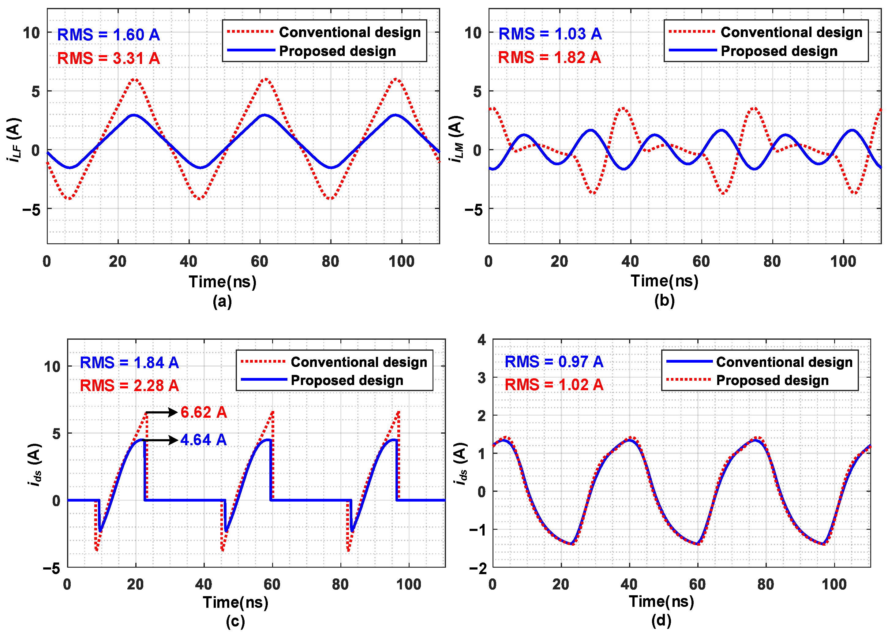
4.1. Branch Current Waveform Comparisons

Waveforms of iLF(t), iLM(t), ids(t) and iLS(t) at RL = 25 Ω are shown in Figure 10. RMS values of branch currents are marked on the figures. With the proposed efficiency optimization design method, the peak and RMS value of branch currents are reduced, thus reducing circling losses and improving the power efficiency of the class Φ2 inverter.

4.2. Loss and Efficiency Comparisons

RMS values of branch currents under different load resistances are summarized in Table 3. Component losses are summarized in Table 4. Parasitic resistances of the proposed design are rLF = 0.21 Ω, rLM = 0.62 Ω, rLS = 0.33 Ω and rds_on = 0.10 Ω. Parasitic resistances of the conventional design are rLF = 0.15 Ω, rLM = 0.60 Ω, rLS = 0.33 Ω and rds_on = 0.10 Ω. Compared with the conventional design, the proposed design method significantly reduces the RMS value of iLF(t) from 3.31 A to 1.60 A at 25 W, while reducing the loss of LF from 1.64 W to 0.54 W. The RMS value of LM is reduced from 1.82 A to 1.03 A, while the loss of LM is reduced from 1.98 W to 0.65 W. The RMS value of LS under different designs are essentially the same, which indicates a similar output power. The RMS value of the power switch is reduced from 2.28 A to 1.84 A, while the loss of the power switch is reduced from 0.52 W to 0.34 W. The total loss is reduced from 4.49 W to 1.84 W. At 18 W and 8 W, the RMS values of branch currents and the total loss are also reduced.

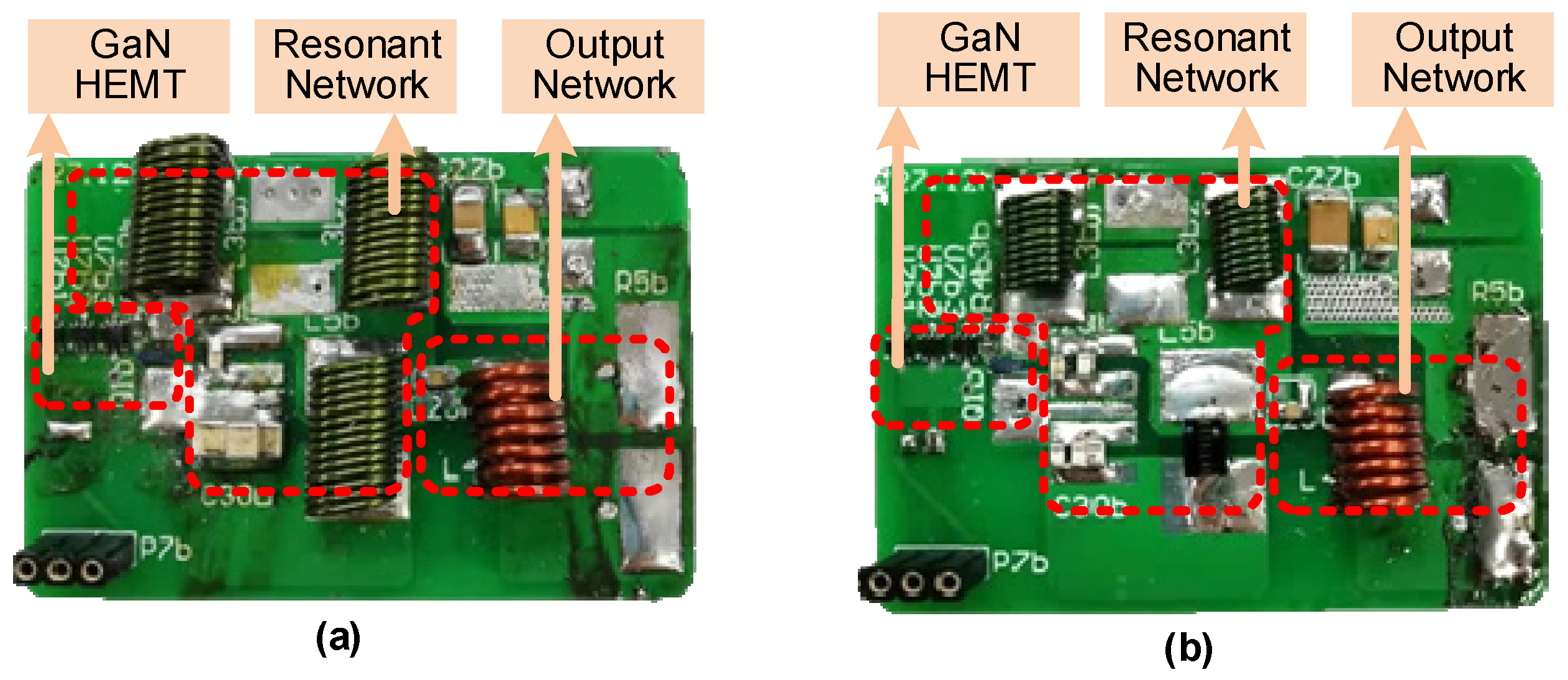
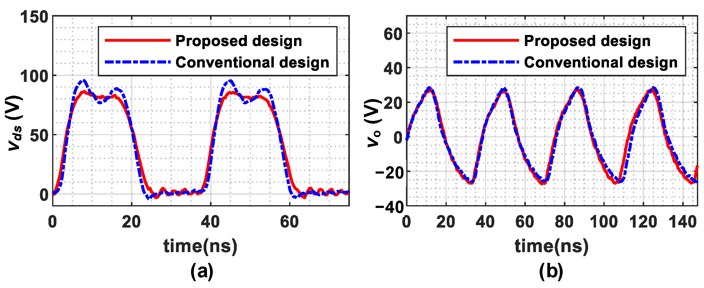
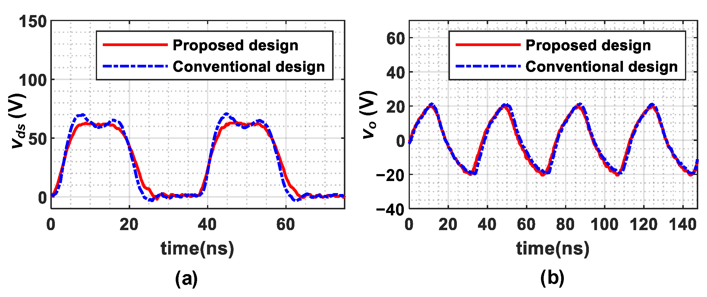
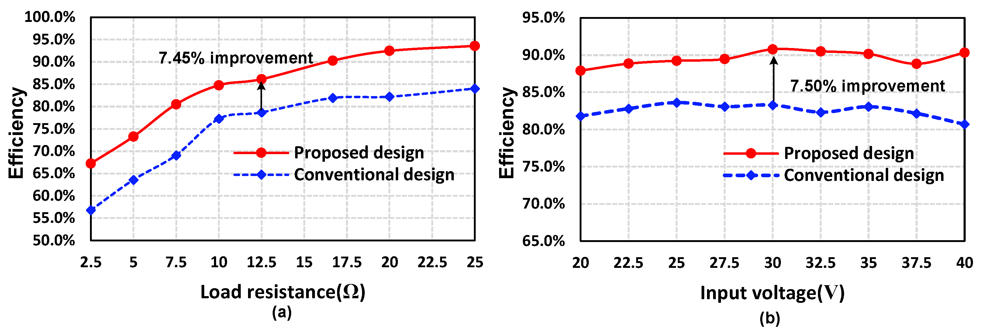
5. Experimental Results

To verify effectiveness of the proposed efficiency optimization design method, two prototypes are built with the conventional and proposed design method, respectively. A block diagram of the prototype is shown in Figure 11, the prototypes are shown in Figure 12, and the main specifications of the prototypes are shown in Table 5. The power switch is EPC2019 from EPC, the gate driver is realized with high-speed buffer NC7WZ17.

5.1. Waveform Comparisons

The voltage waveforms were measured with the oscilloscope MDO3054. Figure 13 shows the waveforms at Vin = 40 V and RL = 25 Ω, Figure 14 shows the waveforms at Vin = 40 V and RL = 16 Ω, and Figure 15 shows the waveforms at Vin = 30 V and RL = 16 Ω. Output voltages of the proposed and conventional design are essentially the same at different working conditions, whereas the proposed design method reduces the harmonic components of the switching node voltage. This indicates smaller circling losses in the resonant network, which improves the overall power efficiency of the class Φ2 inverter.

5.2. Efficiency Comparisons

The input power is obtained by measuring the average input voltage and current with multimeters. The output power is obtained with the value of load resistance and the RMS value of the output voltage. Figure 16a shows the prototype efficiency with respect to load resistance, and Figure 16b shows the prototype efficiency with respect to input voltage. Compared with conventional design, the proposed efficiency optimization design significantly improves the power efficiency over the whole load range. At a rated output power, the proposed design achieves a peak efficiency of 93.6%. Compared with conventional design, an improvement of 9.6% is achieved. Over the whole load range, the power efficiency is improved by more than 7%. The experiments demonstrate that the proposed design method can effectively improve power efficiency of a class Φ2 inverter by reducing the resonant current magnitude and unnecessary circling losses.

6. Conclusions

This paper proposed an efficiency optimization design method for a very high frequency class Φ2 inverter based on an analytical loss model. The analytical expression of the switching node voltage was derived by analyzing its harmonic components. With the result, the circuit was simplified by modeling the power switch as a voltage source. Then, analytical expressions and the RMS value of branch currents were derived to calculate components losses, which form the analytical loss model. Furthermore, the influence of circuit parameters on the total loss and power efficiency were thoroughly analyzed, to derive the optimal design equations and minimize circling losses in the class Φ2 inverter. Finally, the proposed design method was verified by experiments. The proposed harmonic analysis modeling method and analytical losses model can also be used in other resonant topologies to improve power efficiency.

Author Contributions

Conceptualization, M.Z.; Methodology, R.M.; Project administration, A.Z.; Resources, Q.T. and Q.Z.; Validation, Z.L. and T.W.; Writing—original draft, D.Z.; Writing—review & editing, D.Z. and R.M.; D.Z. and R.M. contributed equally to this work. All authors have read and agreed to the published version of the manuscript.

Funding

This work was funded by the National Natural Science Foundation of China under Grant 62074067, the Ministry of Industry and Information Technology of the People’s Republic of China, and Science, and Technology Project of State Grid Corporation of China Headquarters (5700-202258309A-2-0-QZ) Research on low-propagation-delay and high-stability digital gate driver chip technology for high-voltage and high-power silicon carbide (SiC) power device.

Data Availability Statement

The datasets used and/or analyzed during the current study are available from the corresponding author upon reasonable request.

Acknowledgments

This work was supported by Huazhong University of Science and Technology and Beijing Institute of Spacecraft System Engineering.

Conflicts of Interest

The authors declare that they have no conflict of interest.

Appendix A

This appendix provides the SPICE netlist used in LTSPICE simulations.
* SPICE netlist for the proposed design
V1 N005 0 PULSE(0 4 0 1p 1p 13.4n 36.87315n 10000)
L1 N001 N002 138n Rser=0.28
L2 N002 N003 152n Rser=0.1
L3 N002 N006 420n Rser=0.6
C1 N006 0 20.2p
C2 N004 N003 4n
R1 N004 0 25
V2 N001 0 40 Rser=0.1
C3 N001 0 1µ
C4 N002 0 205p Rser=0.2
S1 N002 0 N005 0 MySwitch
D1 0 N002 D
.model D D
.lib C:\Users\10652\Documents\LTspiceXVII\lib\cmp\standard.dio
.model MySwitch SW(Ron=.1 Roff=1Meg Vt=1)
.tran 5u
.backanno
.end
* SPICE netlist for the conventionals design
V1 N005 0 PULSE(0 4 0 1p 1p 15N 36.87315n 10000)
L1 N001 N002 65n Rser=0.28
L2 N002 N003 152n Rser=0.1
L3 N006 N002 56n Rser=0.6
C1 N006 0 150p
C2 N004 N003 4n
R1 N004 0 25
V2 N001 0 40 Rser=0.1
C3 N001 0 1µ
C4 N002 0 262p Rser=0.2
S1 N002 0 N005 0 MySwitch
D1 0 N002 D
.model D D
.lib C:\Users\10652\Documents\LTspiceXVII\lib\cmp\standard.dio
.model MySwitch SW(Ron=.1 Roff=1Meg Vt=1)
.tran 10U
.backanno
.end

References

  1. Perreault, D.J.; Hu, J.; Rivas, J.M.; Han, Y.; Leitermann, O.; Pilawa-Podgurski, R.C.N.; Sagneri, A.; Sullivan, C.R. Opportunities and Challenges in Very High Frequency Power Conversion. In Proceedings of the 2009 Twenty-Fourth Annual IEEE Applied Power Electronics Conference and Exposition, Washington, DC, USA, 15–19 February 2009; pp. 1–14. [Google Scholar]
  2. Xu, D.; Guan, Y.; Wang, Y.; Wang, W. Topologies and control strategies of very high frequency converters: A survey. CPSS Trans. Power Electron. Appl. 2017, 2, 28–38. [Google Scholar] [CrossRef]
  3. Knott, A.; Andersen, T.M.; Kamby, P.; Pedersen, J.A.; Madsen, M.P.; Kovacevic, M.; Andersen, M.A.E. Evolution of Very High Frequency Power Supplies. IEEE J. Emerg. Sel. Top. Power Electron. 2014, 3, 386–394. [Google Scholar] [CrossRef] [Green Version]
  4. Rigot, V.; Phulpin, T.; Sakly, J.; Sadarnac, D. A New 7 kW Air-Core Transformer at 1.5 MHz for Embedded Isolated DC/DC Application. Energies 2022, 1, 5211. [Google Scholar] [CrossRef]
  5. Li, Y.; Ruan, X.; Zhang, L.; Lo, Y. Multipower-Level Hysteresis Control for the Class E DC–DC Converters. IEEE Trans. Power Electron. 2020, 3, 5279–5289. [Google Scholar] [CrossRef]
  6. Zhang, Y.; Feng, Y.; Liu, S.; Wu, J.; He, X. Impedance Matching Method for 6.78 MHz Class-E2-Based WPT System. Energies 2021, 1, 4289. [Google Scholar] [CrossRef]
  7. Liu, C.-Y.; Wang, G.-B.; Wu, C.-C.; Chang, E.Y.; Cheng, S.; Chieng, W.-H. Derivation of the Resonance Mechanism for Wireless Power Transfer Using Class-E Amplifier. Energies 2021, 1, 632. [Google Scholar] [CrossRef]
  8. Zhang, Z.; Zou, X.; Dong, Z.; Zhou, Y.; Ren, X. A 10-MHz eGaN Isolated Class-Φ2 DCX. IEEE Trans. Power Electron. 2017, 3, 2029–2040. [Google Scholar] [CrossRef]
  9. Zou, X.; Zhang, Z.; Dong, Z.; Zhou, Y.; Ren, X.; Chen, Q. A 10-MHz eGaN FETs Based Isolated Class-Φ2 DCX. In Proceedings of the 2016 IEEE Applied Power Electronics Conference and Exposition (APEC), Long Beach, CA, USA, 20–24 March 2016; pp. 2518–2524. [Google Scholar]
  10. Si-Yuan, C.; Jun-Ping, H.; Zi-Fan, L. Resonant DC/DC Converter with Class Φ2 Inverter and Class DE Rectifier based on GaN HEMT. Proceedings of thr 22nd European Conference on Power Electronics and Applications (EPE’20 ECCE Europe), Online, 7–11 September 2020; pp. 1–6. [Google Scholar]
  11. Guan, Y.; Wang, Y.; Wang, W.; Xu, D. A 20 MHz Low-Profile DC–DC Converter with Magnetic-Free Characteristics. IEEE Trans. Ind. Electron. 2020, 6, 1555–1567. [Google Scholar] [CrossRef]
  12. Gu, L.; Zulauf, G.; Stein, A.; Kyaw, P.A.; Chen, T.; Davila, J.M.R. 6.78-MHz Wireless Power Transfer with Self-Resonant Coils at 95% DC–DC Efficiency. IEEE Trans. Power Electron. 2021, 3, 2456–2460. [Google Scholar] [CrossRef]
  13. Choi, J.; Xu, J.; Makhoul, R.; Rivas, J. Design of a 13.56 MHz Dc-to-Dc Resonant Converter using an Impedance Compression Network to Mitigate Misalignments in a Wireless Power Transfer System. Proceedings of 2018 IEEE 19th Workshop on Control and Modeling for Power Electronics (COMPEL), Padova, Italy, 25–28 June 2018; pp. 1–7. [Google Scholar]
  14. Tang, X.; Zeng, J.; Pun, K.P.; Mai, S.; Zhang, C.; Wang, Z. Low-Cost Maximum Efficiency Tracking Method for Wireless Power Transfer Systems. IEEE Trans. Power Electron. 2018, 3, 5317–5329. [Google Scholar] [CrossRef]
  15. Zhang, Y.; Ma, J.; Tang, X. A CMOS Active Rectifier with Efficiency-Improving and Digitally Adaptive Delay Compensation for Wireless Power Transfer Systems. Energies 2021, 1, 8089. [Google Scholar] [CrossRef]
  16. Choi, J.; Ooue, Y.; Furukawa, N.; Rivas, J. Designing a 40.68 MHz Power-Combining Resonant Inverter with eGaN FETs for Plasma Generation. Proceedings of 2018 IEEE Energy Conversion Congress and Exposition (ECCE), Portland, OR, USA, 23–27 September 2018; pp. 1322–1327. [Google Scholar]
  17. Liang, W.; Raymond, L.; Praglin, M.; Biggs, D.; Righetti, F.; Cappelli, M.; Holman, B.; Davila, J.R. Low-Mass RF Power Inverter for CubeSat Applications Using 3-D Printed Inductors. IEEE J. Emerg. Sel. Top. Power Electron. 2017, 5, 880–890. [Google Scholar] [CrossRef]
  18. Stedman, Q.; Gu, L.; Pai, C.N.; Rasmussen, M.; Brenner, K.; Ma, B.; Ergun, A.S.; Davila, J.R.; Khuri-Yakub, B. Compact Fast-Switching DC and Resonant RF Drivers for a Dual-Mode Imaging and HIFU 2D CMUT Array. In Proceedings of the 2019 IEEE International Ultrasonics Symposium (IUS), Glasgow, UK, 6–9 October 2019; pp. 1951–1954. [Google Scholar]
  19. Yanagisawa, Y.; Miura, Y.; Handa, H.; Ueda, T.; Ise, T. Characteristics of Isolated DC–DC Converter with Class Phi-2 Inverter Under Various Load Conditions. IEEE Trans. Power Electron. 2019, 3, 10887–10897. [Google Scholar] [CrossRef]
  20. Guan, Y.; Wang, Y.; Wang, W.; Xu, D. A high-performance isolated high-frequency converter with optimal switch impedance. IEEE Trans. Ind. Electron. 2019, 66, 5165–5176. [Google Scholar] [CrossRef]
  21. Kitazawa, K.; Wei, X.; Katsuki, A.; Hirokawa, M. Analysis and Design of the Class-Φ2 Inverter. In Proceedings of the 44th Annual Conference of the IEEE Industrial Electronics Society, Washington, DC, USA, 21–23 October 2018; pp. 1023–1028. [Google Scholar]
  22. Roslaniec, L.; Jurkov, A.S.; Bastami, A.A.; Perreault, D.J. Design of Single-Switch Inverters for Variable Resistance/Load Modulation Operation. IEEE Trans. Power Electron. 2015, 3, 3200–3214. [Google Scholar] [CrossRef] [Green Version]
  23. Rivas, J.M.; Han, Y.; Leitermann, O.; Sagneri, A.D.; Perreault, D.J. A High-Frequency Resonant Inverter Topology with Low-Voltage Stress. IEEE Trans. Power Electron. 2008, 2, 1759–1771. [Google Scholar] [CrossRef]
  24. Panov, Y.; Huber, L.; Jovanović, M.M. Design Optimization and Performance Evaluation of Class Φ2 VHF DC/DC Converter. Proceedings of 2020 IEEE Applied Power Electronics Conference and Exposition (APEC), New Orleans, LA, USA, 15–19 March 2020; pp. 2170–2177. [Google Scholar]
  25. Lee, K.; Ha, J. Resonant Switching Cell Model for High-Frequency Single-Ended Resonant Converters. IEEE Trans. Power Electron. 2019, 3, 11897–11911. [Google Scholar] [CrossRef]
  26. Guan, Y.; Hu, X.; Zhang, S.; Wang, Y.; Xu, D.; Wang, W. A Novel Single Switch High-Frequency DC/DC Converter and Its Mathematical Model. IEEE Trans. Ind. Appl. 2019, 5, 3877–3888. [Google Scholar] [CrossRef]
  27. Ma, J.; Asiya; Wei, X.; Nguyen, K.; Sekiya, H. Analysis and Design of Generalized Class-E/F2 and Class-E/F3 Inverters. IEEE Access 2020, 8, 61277–61288. [Google Scholar] [CrossRef]
Figure 1. Topology of a VHF class Φ2 inverter.
Energies 15 08572 g001
Figure 2. Switch voltage with different harmonics: (a) 1st and 3rd harmonics; (b) 1st and 2nd harmonics.
Energies 15 08572 g002
Figure 3. Voltage source equivalent model of a VHF class Φ2 inverter.
Energies 15 08572 g003
Figure 4. Circuit model for a class Φ2 inverter considering inductor parasitic resistance and power switch on-resistance.
Energies 15 08572 g004
Figure 5. Current waveforms of branch currents under different k1 values when selecting k2 = 1.1. (a) waveforms of iLF(t); (b) waveforms of iLM(t); (c) waveforms of ids(t); (d) waveforms of iLS(t).
Energies 15 08572 g005
Figure 6. RMS values of branch currents under different k1 values when selecting k2 = 1.1. (a) RMS values of iLF(t); (b) RMS values of iLM(t); (c) RMS values of ids(t); (d) RMS values of iLS(t).
Energies 15 08572 g006
Figure 7. Current waveforms of branch currents under different k2 values when selecting k1 = 10. (a) waveforms of iLF(t); (b) waveforms of iLM(t); (c) waveforms of ids(t); (d) waveforms of iLS(t).
Energies 15 08572 g007
Figure 8. RMS values of branch currents under different k2 values when selecting k1 = 10. (a) RMS values of iLF(t); (b) RMS values of iLM(t); (c) RMS values of ids(t); (d) RMS values of iLS(t).
Energies 15 08572 g008
Figure 9. Total loss and overall power efficiency with respect to k1 and k2: (a) total loss; (b) power efficiency.
Energies 15 08572 g009
Figure 10. Waveforms of iLF(t), iLM(t), ids(t) and iLS(t) with different design methods. (a) Waveforms of iLF(t); (b) waveforms of iLM(t); (c) waveforms of ids(t); (d) waveforms of iLS(t).
Energies 15 08572 g010
Figure 11. Block diagram of the prototype.
Energies 15 08572 g011
Figure 12. Class Φ2 inverter prototypes with different design methods: (a) proposed method; (b) conventional design method.
Energies 15 08572 g012
Figure 13. Voltage waveforms of the class Φ2 inverter at Vin = 40 V, RL = 25 Ω. (a) Switching node voltage; (b) output voltage.
Energies 15 08572 g013
Figure 14. Voltage waveforms of the class Φ2 inverter at Vin = 40 V, RL = 16 Ω. (a) Switching node voltage; (b) output voltage.
Energies 15 08572 g014
Figure 15. Voltage waveforms of the class Φ2 inverter at Vin = 30 V, RL = 16 Ω. (a) Switching node voltage; (b) output voltage.
Energies 15 08572 g015
Figure 16. Prototype efficiency under different working conditions. (a) Efficiency with respect to load resistance when Vin = 40 V; (b) efficiency with respect to input voltage when RL = 16 Ω.
Energies 15 08572 g016
Table 1. Main specifications of the class Φ2 inverter.
ParametersValues
Switching frequency27.12 MHz
Input voltage40 V
Output power25 W
Load resistance2.5–25 Ω
Table 2. Circuit parameters with different design methods.
ParametersProposed Design MethodConventional Design Method [23]
LF138 nH65 nH
CF205 pF262 pF
LM420 nH56 nH
CM20.2 pF150 pF
LS152 nH152 nH
CS4 nF4 nF
RL25 Ω25 Ω
Table 3. RMS values of branch currents.
ComponentRL = 25 ΩRL = 10 ΩRL = 5 Ω
ProposedConventionalProposedConventionalProposedConventional
LF1.60 A1.60 A1.60 A3.34 A1.60 A3.34 A
LM1.03 A1.03 A1.56 A2.22 A1.56 A2.22 A
LS0.97 A0.97 A1.33 A1.37 A1.33 A1.37 A
Power switch1.84 A1.84 A2.34 A2.76 A2.34 A2.76 A
Table 4. Component losses of the class Φ2 inverter.
ComponentRL = 25 ΩRL = 10 ΩRL = 5 Ω
ProposedConventionalProposedConventionalProposedConventional
LF0.54 W1.64 W0.54 W1.67 W0.51 W1.66 W
LM0.65 W1.98 W1.51 W2.96 W1.83 W3.31 W
LS0.31 W0.34 W0.58 W0.61 W0.67 W0.70 W
Power switch0.34 W0.52 W0.55 W0.76 W0.59 W0.80 W
Total loss1.84 W4.49 W3.18 W6.01 W3.60 W6.48 W
Table 5. Circuit parameters with different design methods.
ParametersProposed Design MethodConventional Design Method
LF140 nH60 nH
CF200 pF290 pF
LM430 nH56 nH
CM20 pF153 pF
LS150 nH150 nH
CS4.7 nF4.7 nF
RL25 Ω25 Ω
Power switchEPC2019EPC2019
Gate driver3 NC7WZ173 NC7WZ17
Publisher’s Note: MDPI stays neutral with regard to jurisdictional claims in published maps and institutional affiliations.

