Article

Steady-State Analysis and Optimal Design of an LLC Resonant Converter Considering Internal Loss Resistance

1
Department of Electronics Engineering, Cheongju University, Cheongju 28503, Korea
2
Department of Electrical & Control Engineering, Cheongju University, Cheongju 28503, Korea
*
Author to whom correspondence should be addressed.
Energies 2022, 15(21), 8144; https://doi.org/10.3390/en15218144
Submission received: 28 September 2022 / Revised: 17 October 2022 / Accepted: 26 October 2022 / Published: 1 November 2022
(This article belongs to the Special Issue Advanced DC-DC Power Converters and Switching Converters II)

Abstract

:
In this paper, a steady-state model of an LLC resonant half-bridge converter with internal loss resistance is proposed, in order to maximize power conversion efficiency, and steady-state characteristic equations of DC voltage gain and input impedance are derived for the optimal design of the converter. First, to confirm the validity of the steady-state characteristic equation and the optimal design process, a prototype converter with a maximum output of 2 kW was designed. Through comparison of simulation, calculation, and experimental results obtained from the prototype test, it is shown that the calculation results proposed in this paper were closer to the experimental results than the calculation results obtained under the lossless condition. In addition, the relationship between the switching frequency and the load current of the prototype was compared, in order to determine the operating range of the switching frequency, which is important in the converter design stage. In this case, it was confirmed that the calculated value reflecting the internal loss showed a close result. In conclusion, we confirm the usefulness of the analysis results reflecting the internal loss resistance proposed in this paper and the optimal design process.

1. Introduction

The climate crisis has been steadily emerging, where the biggest cause of climate change is known to be greenhouse gas and carbon emissions. There is an urgent need for low-loss power conversion technology that can reduce carbon emissions in the process of generating, distributing, and consuming power energy. Therefore, the technical demand for a high-efficiency power conversion device for the efficient use of limited electric energy is increasing. A switching power supply with AC input can be divided into an AC-DC rectifier and a DC-DC converter. In particular, the DC-DC converter uses various types of circuit methods, based on the position of the power semiconductor switch and the structure of the transformer. Among the insulated circuit methods using transformers, the LLC resonant converter, which is suitable for medium- to high-capacity scenarios, is a circuit method that has attracted attention in various industrial fields, due to its advantages such as low loss, high efficiency, and small number of parts needed [1,2,3]. The LLC resonant converter has low switching loss as well as low voltage and current surges, as both the main switch and the rectification switch operate in a soft-switching condition. In addition, it is known that the effective current value of the device is small, such that the conduction loss is small and, thus, high-efficiency power conversion is achievable [4,5].
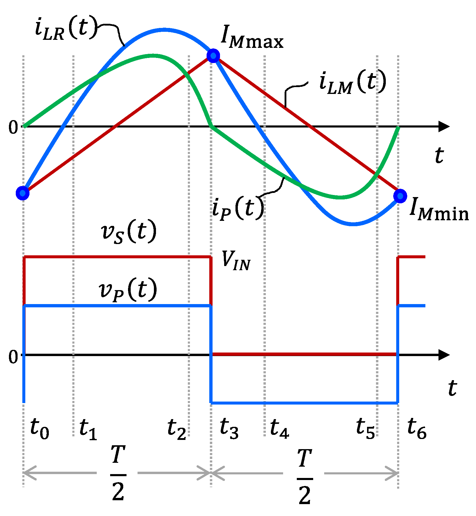
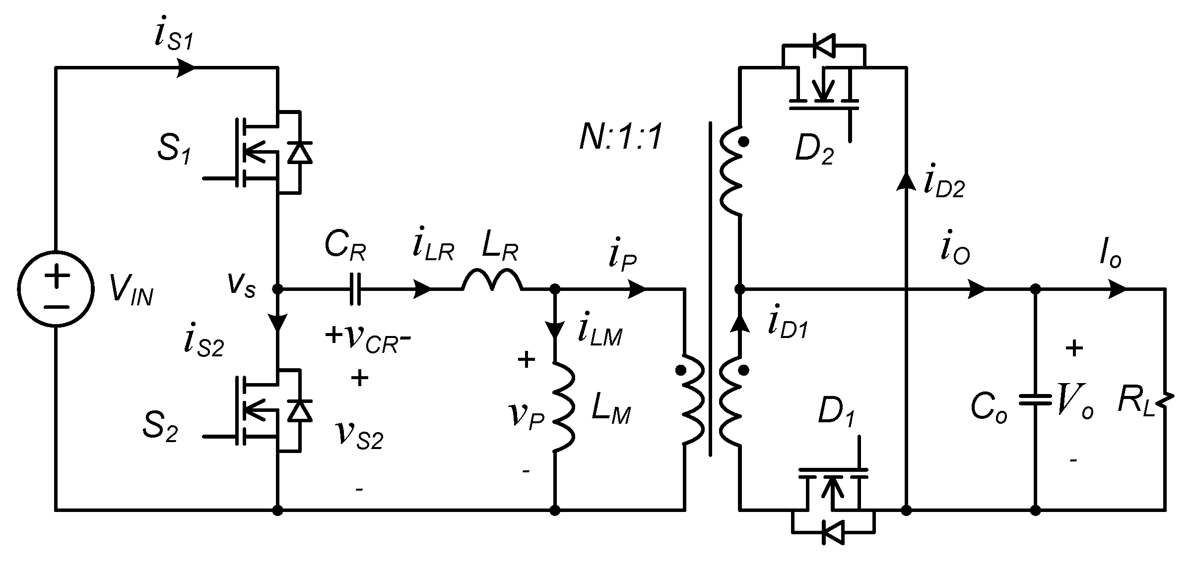
Figure 1 shows the basic circuit structure of a half-bridge LLC resonant converter. In the figure, the main switches of the converter are S1 and S2, and the two switches are controlled with a fixed duty of 50% and a variable switching frequency. On the primary side of the transformer, there are three resonant components: The resonant capacitor C R , resonant inductor L R , and magnetizing inductor L M . Meanwhile, the rectifying diode, output capacitor, and load resistor are shown on the secondary side. Figure 2 shows the operation waveform of the LLC resonant converter operating in steady-state. As can be seen from the figure, the primary side voltage v p of the transformer switches its polarity with the same area size due to the secondary side output voltage V o of the transformer, while the current i L M of the magnetizing inductor, which is configured in parallel, operates as a triangular waveform with a constant slope [6,7,8]. As the current resonates with the two resonant components C R and L R , the main switch and the diode show zero current switching (ZCS) characteristics and so the LLC resonant converter has low switching loss and high-efficiency power conversion characteristics. Meanwhile, due to the resonance waveform having the same sized area, the magnetic flux density of the core uses both positive and negative polarities for the primary current of the transformer. Therefore, the core size and core loss may be reduced by increasing the core utilization [9,10,11].
In general, the steady-state characteristic design formula used in the circuit design process of LLC resonant converters is based on an ideal equivalent model that does not reflect internal power loss. For this reason, it is well-known that there exists a difference between the design result of an LLC resonant converter and the operating characteristics of the actual circuit. In particular, errors occur in the operating switching frequency range, which is an important criterion when designing a converter [12,13]. In addition, these errors are the biggest obstacle to the optimal design of important devices, such as transformers and inductors, whose basic characteristics change depending on the operating frequency.
In this paper, an AC equivalent circuit model considering the internal loss resistance of the LLC resonant converter is proposed. From the proposed AC equivalent circuit, important steady-state characteristic equations necessary for converter design, such as DC voltage gain and input impedance, are derived. In order to verify the validity of the results of the equivalent circuit and the steady-state characteristic equation, the calculation result of the steady-state characteristic, as well as those of the simulation and experimental circuit, were compared and confirmed [14,15,16,17]. In particular, the steady-state characteristic equation was applied to the optimal design process of the LLC resonant converter, in order to determine the main element values, and the results were used in an experimental circuit with a resonant frequency of 125 kHz and a maximum output of 2 kW.

2. Steady-State Analysis of LLC Resonant Converter

2.1. AC Equivalent Circuit

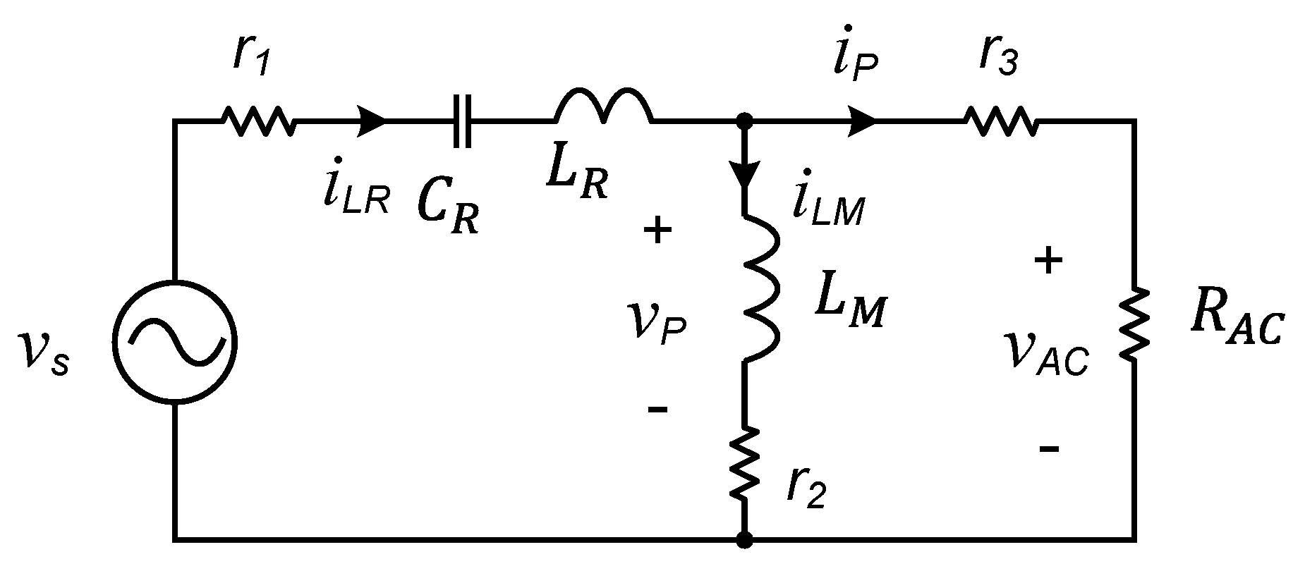
Figure 3 shows the equivalent circuit expressing the series parasitic resistances of each element in the LLC resonant converter of Figure 1. In the figure, the main switch is an ideal switch, the output capacitor and the load resistance are equivalent to a constant voltage, and the internal parasitic resistance is shown in series with the important components. In particular, the equivalent circuit in Figure 3 is divided into two equivalent circuits for each state, according to the operating state of switches S1 and S2 when operating in steady-state, as shown in Figure 4. In general, a non-switching linear equivalent circuit is required to derive the steady-state characteristic expression reflecting the internal loss resistance. In a previous study, the fundamental harmonic approximation (FHA) approximation method [18,19], which could approximate a square wave by a sine wave, has been used. In this paper, the internal power loss resistance is reflected in the circuit, and the input and output voltages are converted using an FHA approximation method to propose an equivalent circuit with loss resistance, as shown in Figure 5. At this time, existing parasitic resistors in each major element in Figure 3 could be simplified to three series resistors r 1 , r 2 , and r 3 , as shown in the equivalent circuit of Figure 5. The load resistance R L is expressed as the AC equivalent resistance R A C converted to the primary side of the transformer, as in Equation (1):
R A C = 8 N 2 π 2 R L .

2.2. DC Conversion Ratio

First, Equations (2)–(6) are defined to derive the steady-state characteristic expression:
K L = L M L R ,
Z o = L R C R ,
ω o = 1 L R   C R ,
ω n = ω f ω o ,
Q = Z o R A C ,
where
  • Z o denotes the characteristic impedance;
  • L M denotes the magnetizing inductance;
  • L R denotes the resonant inductance;
  • K L denotes the inductance ratio;
  • C R denotes the resonant capacitor;
  • ω o denotes the resonant angular frequency;
  • ω n denotes the angular normalized frequency;
  • ω f denotes the angular switching frequency.
In order to obtain the DC voltage gain in the steady-state for the AC equivalent circuit of Figure 5, the voltage gain M is defined as in Equation (7). At this time, the ratio between the input voltage v s t and the output voltage v A C t can be calculated through the impedance ratio of the equivalent circuit, and the result is shown as Equation (8), where the internal resistance r K used in the equation is given in Equation (9).
M = v A C t v s t
M = r 2 Z o + j ω n K L   K L r K Z o 2 K L + 1 ω n 2 Q + j ω n r 2 + r 3 R A C + 1 + r 1 + r 3 R A C + 1 K L 1 ω n 2 r 2 + r 3 R A C + 1
r K = r 1 r 2 + r 2 r 3 + r 3 r 1 + r 1 R A C + r 2 R A C ,
In order to calculate only the magnitude of the input and output voltage gain M in Equation (8), the absolute values of both sides need to be obtained, and the result is shown in Equation (10). Meanwhile, it is expected that the products of the parasitic resistances r 1 r 2 , r 2 r 3 , and r 3 r 1 among the internal resistances of Equation (9) are very small; if the values of the products of the parasitic resistances are assumed to be zero, then Equation (11) can be derived. Assuming that each parasitic resistance is equal to the same resistance r , as in Equation (12), it is arranged as Equation (13). At this time, the ratio between the internal parasitic resistance r and the characteristic impedance Z o is defined as the internal loss equivalent resistance R K , expressed as in Equation (14).
M = r 2 Z o 2 + ω n 2 K L 2 K L 2 r K Z o 2 K L + 1 ω n 2 2 Q 2 + ω n 2 r 2 + r 3 R A C + 1 + r 1 + r 3 R A C + 1 K L 1 ω n 2 r 2 + r 3 R A C + 1 2 .  
r K r 1 + r 2 R A C
r 1 r 2 r 3 r
r 2 + r 3 R A C r 1 + r 3 R A C r 1 + r 2 R A C 2 r R A C = 2 Q r Z o = 2 Q R K
R K = r Z o
From the above assumptions and approximations, the DC input and output voltage ratio M of Equation (10) can be arranged as Equations (15) and (16). If the internal loss equivalent resistance R K is 0, it becomes Equation (17). Equation (17) is the same as the DC input and output voltage gain equation obtained from the existing lossless AC equivalent circuit. Therefore, Equation (16) can be used as the steady-state DC voltage gain characteristic expression of the LLC resonant converter reflecting the internal loss resistance depicted in Figure 3.
M = 2 N V o V I N
M = 1 + R K ω n   K L 2   2 Q R K + 1 2 1 + 1 K L 1 1 ω n 2 2 + 2 R K ω n Q K L + 1 ω n ω n 2 Q 2
M = 1 1 + 1 K L 1 1 ω n 2 2 + 1 ω n ω n 2 Q 2

2.3. Frequency Characteristics of Voltage Gain

The frequency characteristics of the DC voltage gain in Equation (15) for the LLC resonant converter reflecting the internal loss resistance were analyzed. Table 1 shows each convergence value for the normalized angular velocity ω n in Equation (15). First, when Q = 0, the load current is 0 from Equations (1) and (6) and in this case, the LLC resonant converter is in a no-load state. When the normalized angular velocity ω n approaches 0, the voltage gain is 0; when the normalized angular velocity ω n approaches infinity, the voltage gain converges to a constant value K L K L + 1 , expressed in terms of the inductance ratio K L . In addition, when the normalized angular velocity is 1, it is expressed as a value reflecting the internal loss equivalent resistance R K ; it can be seen that the voltage gain infinitely increases when the normalized angular velocity is a specific value 1 K L + 1 . When the Q value is large, the voltage gain is 0 at a low normalized angular velocity; when the normalized angular velocity ω n is 1, it can be seen that the voltage gain is expressed as a value reflecting the value of the internal loss resistance. In particular, when the normalized angular velocity is 1 and the internal loss resistance value is 0 in both cases, the voltage gain becomes 1. This result is the same as the frequency response characteristic of the existing voltage gain [20,21,22].
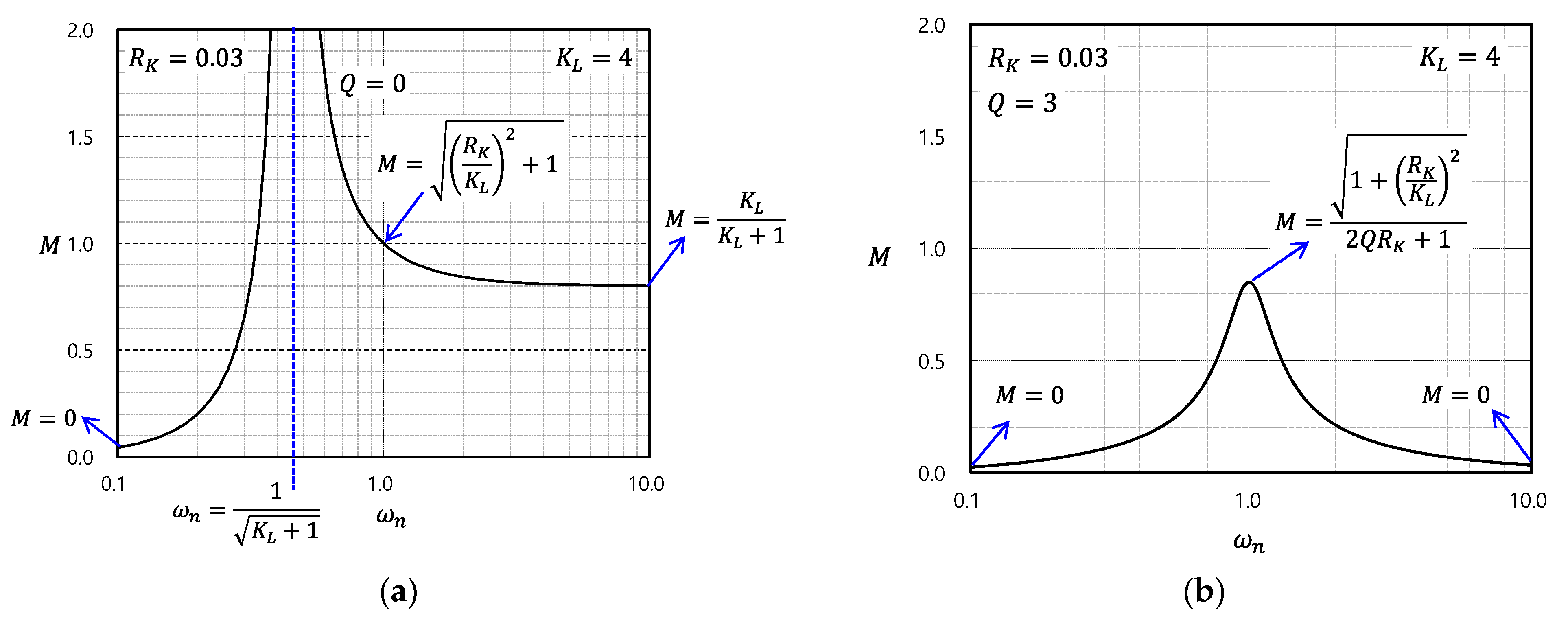
Figure 6 shows the frequency characteristics of the voltage gain when the inductance ratio K L is 4. Figure 6a shows when Q is 0, and Figure 6b shows when Q is 3. Figure 6a shows the frequency characteristics of the LLC resonant converter voltage gain under the no-load condition. As can be seen from the figure, as for the conventional voltage gain, when the normalized angular velocity is 1 K L + 1 , the voltage gain increases infinitely; meanwhile, when the normalized angular velocity increases, the voltage gain converges to K L K L + 1 . However, when ω n is 1, M has a value greater than 1, due to internal loss. When Q is 3, unlike the existing frequency characteristics, when ω n is 1, the voltage gain is not 1 but, instead, a peak value smaller than 1 reflecting the internal loss resistance [23,24]. The frequency characteristic in Figure 6 is the same as the convergence value in Table 1.
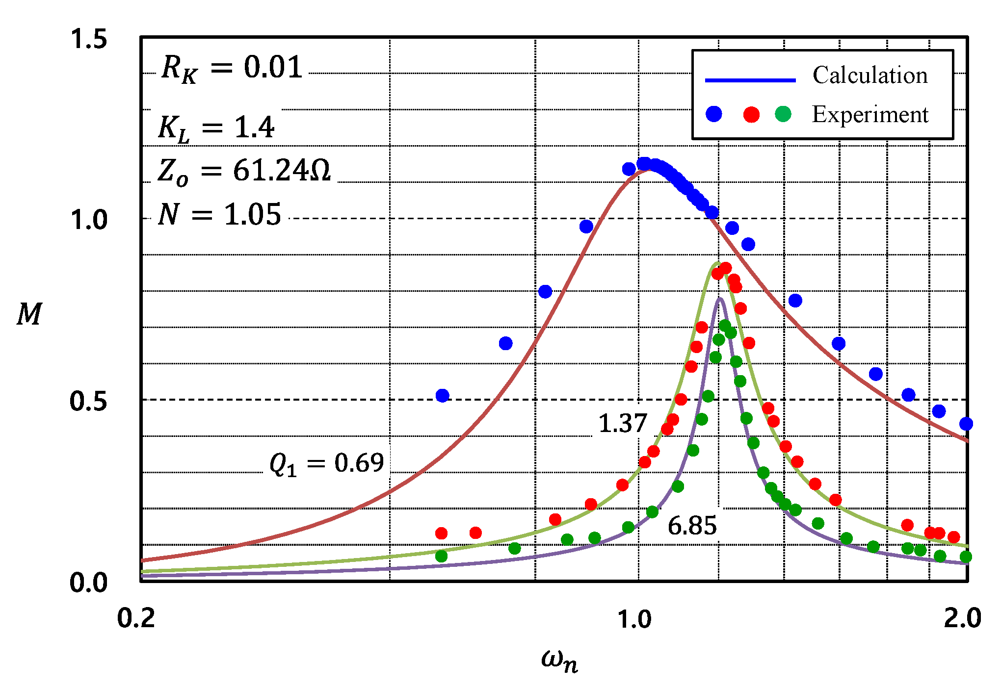
Figure 7 shows the voltage gain frequency characteristics for several Q values. Figure 7a shows a characteristic graph when the internal loss resistance R K is 0, and Figure 7b shows a characteristic graph when the internal loss resistance R K is 0.03. As can be seen from Figure 7b, when ω n is 1, if there is an internal loss resistance, the voltage gain does not reach 1, and it can be seen that the peak value decreases as Q increases. Figure 8 shows the voltage gain obtained by comparing the calculated value and the experimental value when the inductance ratio K L is 1.4, the transformer turn ratio N is 1.05, and the characteristic impedance Z o is 61.24. In the figure, Q is set as 0.69, 1.37, or 6.85, and when ω n is 1, it can be seen that the voltage gain does not reach 1 and the peak value decreases as Q increases. This result is consistent with the above description, and the fact that the experimental value and the calculated value were consistent (within a certain range) supports the validity of the steady-state characteristic expression of Equation (15).

2.4. Input Impedance Characteristics

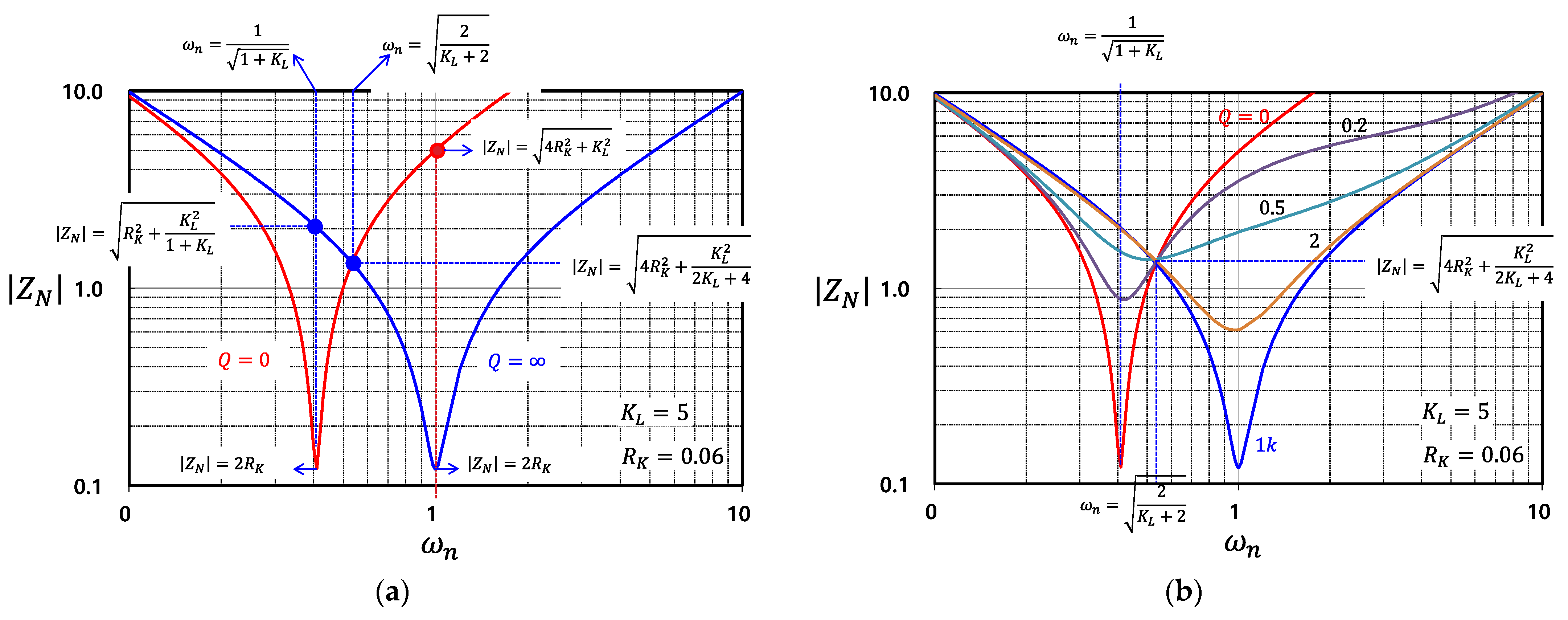
Figure 9 shows the equivalent circuits used to analyze the input impedance characteristics of the AC equivalent circuit with internal loss resistance. Figure 9a is the circuit used to find the input impedance for the AC equivalent circuit of Figure 5, and Figure 9b is the equivalent circuit in which the components in each branch are expressed by their respective impedances. Equation (18) was used to derive the normalized input impedance Z N from Figure 9a. In this case, the normalized input impedance Z N is the ratio of the input impedance Z I N and the characteristic impedance Z o . If Equation (18) is divided into real and imaginary terms and the absolute value is taken, Equation (19) is obtained [25,26]. If the internal resistance is set to 0 in Equation (19), Equation (20) is obtained, and it can be seen that this is the same as the existing lossless input impedance characteristic equation. In order to analyze the frequency characteristics of the normalized input impedance Z N , Equations (21) and (22) were obtained by substituting zero and infinity for Q, respectively. Table 2 summarizes the convergence results of the normalized input impedance Z N , according to the normalized angular velocity ω n . It was found that the normalized angular velocity ω n , which becomes the lowest value of the normalized input impedance Z N , differs depending on the Q value; in particular, each lowest value corresponds to about twice the internal equivalent resistance R K . The junction of the two conditions can be derived from the conditional expression of Equation (23), and the normalized angular velocity ω n and the normalized input impedance Z N at this time are expressed by Equations (24) and (25), respectively. Figure 10 shows the frequency characteristic graph of Equation (19), and the results of Table 2 are reflected in the graph [27].
Z N = Z I N Z o = R K + j ω n j 1 ω n + R K + j ω n R K Q + 1 K L 1 + 2 R K Q + j ω n Q K L
Z N = R K + R K + ω n 2 R K Q + 1 Q K L 2 1 + 2 R K Q 2 + ω n 2 Q 2 K L 2 2 + ω n 1 ω n + ω n K L 1 + 2 R K Q 2 + ω n 2 Q 2 K L 2 2
Z n = Z I N Z o = ω n 2 K L 2 Q 1 + ω n 2 K L 2 Q 2 2 + ω n 1 ω n + ω n K L 1 + ω n 2 K L 2 Q 2 2
Z N Q = 0   = 4 R K 2 + ω n 1 ω n + ω n K L 2
Z N Q = = R K + R K ω n 2 K L 2 4 R K 2 + ω n 2 K L 2 2 + ω n 1 ω n 2
Z N Q = 0   = Z N Q =
ω n = 2 K L + 2
Z N = 4 R K 2 + K L 2 2 K L + 4

3. Optimal Design of LLC Resonant Converter

3.1. Optimal Design Process

The design process of an LLC resonant converter with internal loss, using the steady-state analysis results mentioned in the previous section, is detailed here. First of all, it is necessary to determine the maximum Q value in the DC voltage gain range required for design, as in the previous research. The peak value of M appearing at a specific Q value occurs at the lowest point of the normalized input impedance of Equation (26) and, in this case, it can be obtained under the condition that the imaginary term is 0, as in Equation (27). Equation (28), which summarizes Equation (27), is the normalized angular velocity ω n   m a x at which M becomes maximum for a specific Q value [28].
Z N = R K + R K + ω n 2 R K Q + 1 Q K L 2 1 + 2 Q R K 2 + ω n 2 Q 2 K L 2 + j ω n 1 ω n + ω n K L 1 + 2 Q R K 2 + ω n 2 Q 2 K L 2
ω n   m a x 1 ω n   m a x + ω n   m a x K L 1 + 2 Q R K 2 + ω n   m a x 2 Q 2 K L 2 = 0
ω n   m a x = A 2 + B A 1 2
A = K L + B 2 Q m a x 2 K L 2 1 2 ,     B = 1 + 2 R K Q m a x 2    
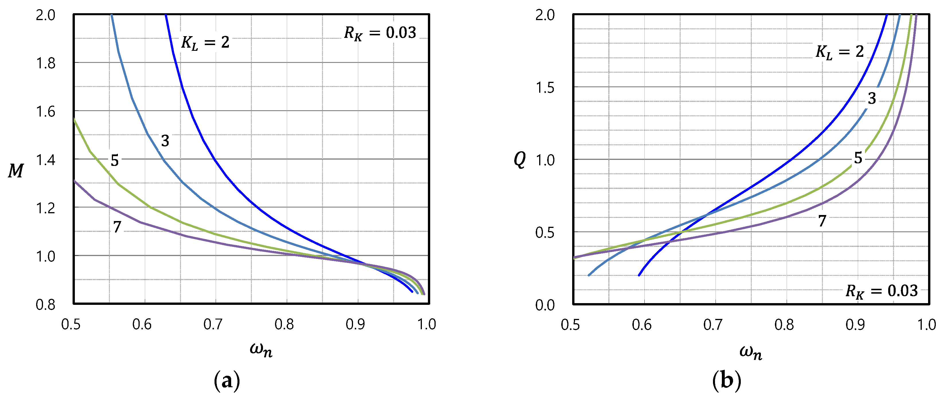
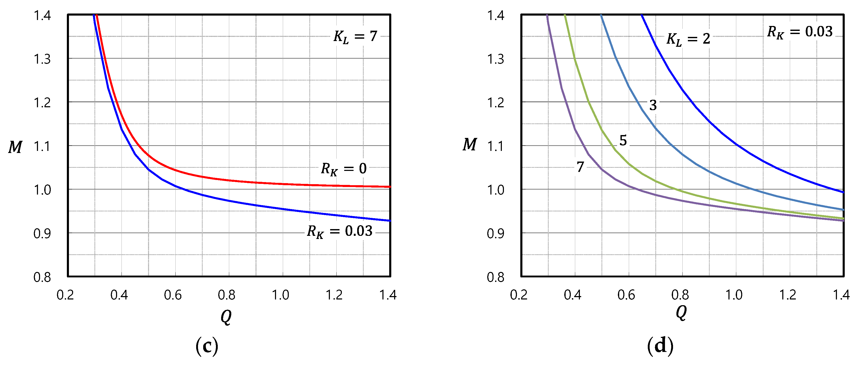
Substituting the result of Equation (28) into Equation (29) for DC voltage gain, an expression satisfying Equation (30) is obtained, where Q is proportional to the load current as in Equation (31). Figure 11 is a graph of the results obtained from Equations (27) and (30). Figure 11a is the graph from Equation (30) for each K L value, and Figure 11b is the graph from Equation (27) for each K L value. Figure 11c is a QM graph according to the internal equivalent resistance, from which it can be seen that the peak value of M is relatively low when there is an internal equivalent resistance in the figure [29,30]. Figure 11d shows the peak value of M at a specific value of Q. In general, this graph serves as a criterion for finding an important Q value in the design process of an LLC resonant converter under a given DC voltage gain.
M p e a k = 1 + R K ω n   K L 2   2 Q m a x R K + 1 2 1 + 1 K L 1 1 ω n 2 2 + 2 R K ω n Q m a x K L + 1 ω n ω n 2 Q m a x 2
2 Q R K + 1 2 1 + 1 K L 1 1 ω n 2 2 + 2 R K ω n Q K L + 1 ω n ω n 2 Q 2 1 + R K ω n   K L 2 M 2 = 0
Q = Z o π 2 8 N 2 V o I o
Figure 12 below shows the operation range of the LLC resonant converter, partially enlarged in the DC voltage gain characteristic graph of Figure 7. In the figure, M takes the maximum and minimum values of the normalized angular velocity ω n , according to the input voltage range, and the operation area is formed as a closed loop connecting the points A, B, C, and D. At this time, within a specific Q value range proportional to the load current, the peak value of M can be determined as in Equation (27). In order to design a stable control system in the LLC resonant converter, it is necessary to ensure that the peak value of M is on the outer left side of the operating range, as shown in the figure [31].
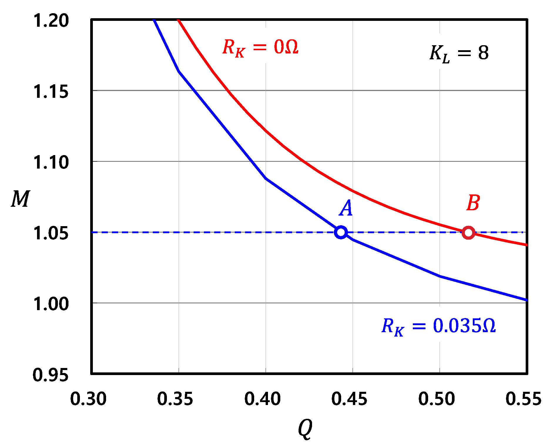
Table 3 shows the design specifications of the LLC resonant converter designed in this paper. The input voltage range is 360–400 V, the maximum output is about 2 kW, the output voltage is 54 V, the resonance frequency is 125 kHz, and the inductance ratio is 8. At the normal input voltage of 390 V in Table 3, the transformer turn ratio is given as in Equation (32). Although the maximum output is 2 kW when the maximum output including the margin is 2.250 kW, the AC resistance R A C is as given in Equation (33). The maximum and minimum voltage gain, with respect to the input voltage, are shown in Equations (34) and (35), respectively. If the peak value of M for Q is obtained from Equation (30), it can be obtained from two points, as shown in Figure 13. Point A is the case with internal equivalent resistance, and point B is the lossless case [32]. From the figure, it can be seen that Q is about 0.44 at point A, and about 0.52 at B. In general, the difference in Q value affects the operating switching frequency range. The characteristic impedance is expressed in Equation (37), and the resonant components that play an important role in the operation of the converter are expressed in Equations (38)–(40).
N = V I N n o m 2 V o = 380 2 × 54 = 3.5
R A C = 8 N 2 V o 2   π 2 P o m a x = 8 × 3.5 2 × 54 π 2 × 2250 = 12.9   Ω
M m i n = 2 N V o V I N m a x = 2 × 3.5 × 54 400 = 0.95
M m a x = 2 N V o V I N m i n = 2 × 3.5 × 54 360 = 1.05
Q m a x = 0.44
Z o = Q R A C = 5.7   Ω
C R = 1 2 π f o Z o = 226   nF
L R = Z o 2 π f o = 7.3   μ H
L M = K L L R = 58.4   μ H

3.2. Circuit Simulation Results and Comparison

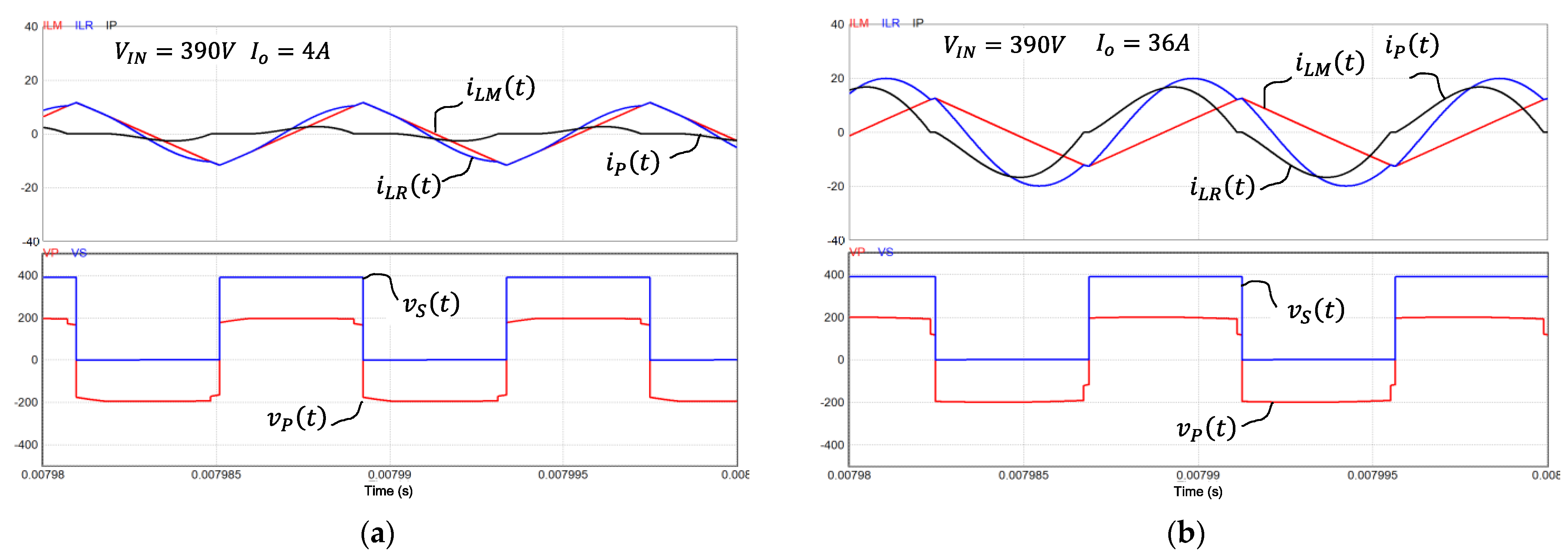
To verify the LLC resonant converter design result in the previous section, a circuit simulation was performed in this paper. We used the simulation software PSIM 11.0, and the circuit diagram is shown in Figure 14. In the figure, the internal resistances of the converter reflect the internal losses. A photocoupler was applied to isolate the control signal, and a frequency-limited voltage-controlled oscillator (VCO) circuit was used to stabilize the output voltage. Figure 15 shows the steady-state result waveform of the PSIM simulation obtained under two load conditions. In Figure 15a, the load current is about 4 A, while in Figure 15b the load current is about 36 A—the maximum output. At a typical input voltage of 390 V, the switching frequency was close to the resonance frequency, and both the magnetization current and the resonance current showed stable waveforms. This result is considered to indirectly confirm that the previously designed main resonant components were designed relatively appropriately [33,34,35].

4. Experimental Results

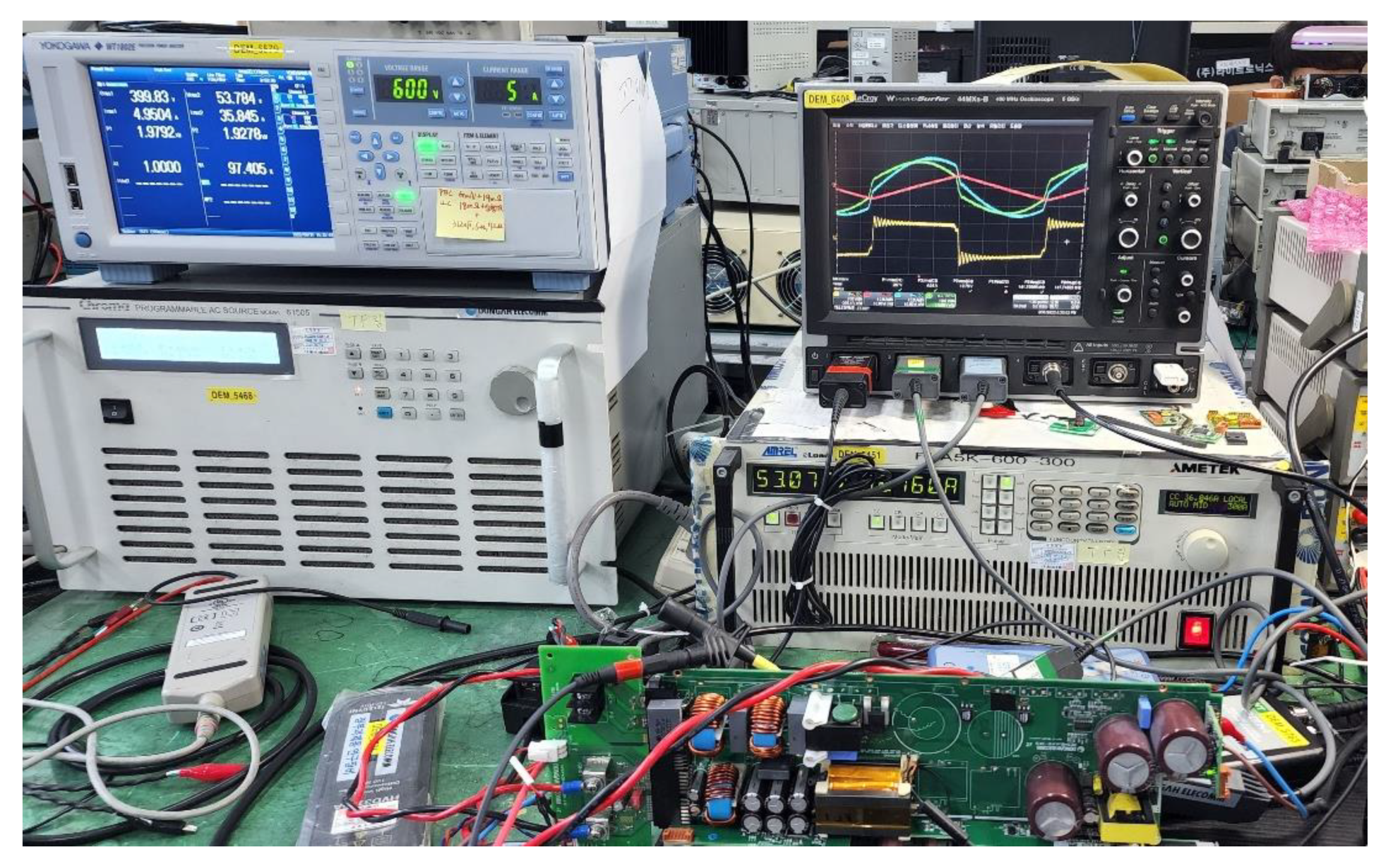
In order to verify the design result of the LLC resonant converter in the previous section, an experimental circuit was constructed and its characteristics were analyzed. Table 4 shows the models and electrical specifications of the main components used in the experimental circuit. In Figure 16, Vishay’s 650 V class MOSFET was used for the main switch and the gate on-resistance was 39 mΩ. Six resonant capacitors were used in parallel to increase the current rating, and a ferrite core (PQ3552 model) was used for the transformer. The rectifying diode on the secondary side of the transformer applied a synchronous rectifier circuit to reduce the rectification loss, and the on-resistance of the rectifier switch was 5.1 mΩ. Figure 17 provides a photograph of the experimental configuration, which shows the experimental circuit and measuring instruments used for the test. The power supply used in the experiment was a 61,505 from Chroma (Foothill Ranch, CA, USA), the electronic load was a PLA5K-600-300 from Amrel (San Diego, CA, USA), the power analyzer was a WT1802E from YOKOGAWA (Tokyo, Japan), and the oscilloscope was a 44MXS-B from LeCroy (Chestnut Ridge, NY, USA). Figure 18 shows the steady-state operation waveform of the experimental circuit. Figure 18a,b shows the results when the input voltage was 390 V whereas Figure 18c,d shows the results when the input voltage was 400 V. Figure 18a,c shows when the load current was at 4 A whereas Figure 18b,d shows when the load current was at 36 A. In the figure, the waveforms represent the resonance current i L R , magnetizing current i L M , the transformer primary current i p , and the transformer primary voltage v p , from the top. In the figure, each current and voltage waveform maintained a stable state, with respect to load change and input voltage change, and was controlled at an appropriate switching frequency state. In particular, when the input voltage was 390 V, the waveforms of the experimental result and the PSIM simulation result were similar.
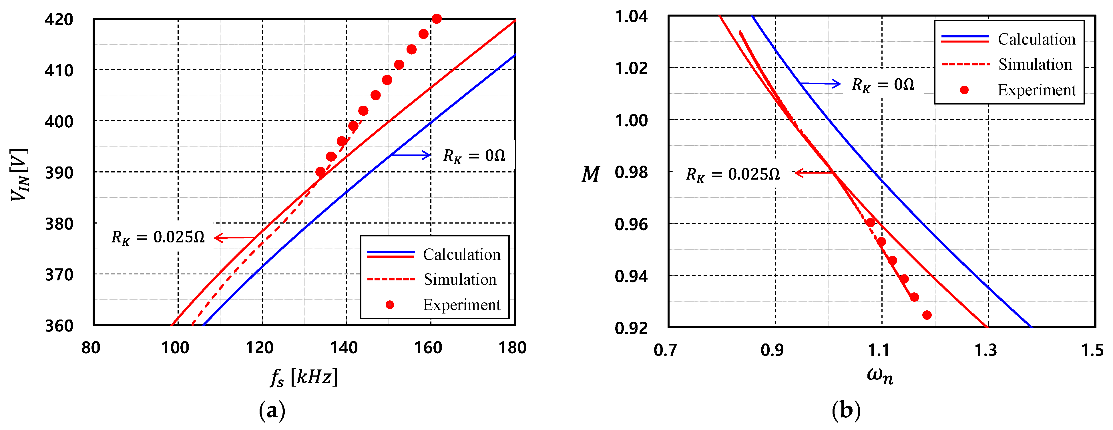
Figure 19 shows the relationship between the DC voltage gain and frequency measured in the experimental circuit. Figure 19a shows the comparison of experimental values, calculated values, and simulation results of input voltage and switching frequency when the load current was maintained at 4 A. Figure 19b shows the results for the voltage gain M versus the normalized angular velocity ω n . When the load was small, the difference between the case with and without the internal equivalent resistance was not large. The difference between the experimental value and the calculated value in the figure is thought to be due to the fundamental harmonic approximation (FHA) approximation method, which increases the error at no load, being used for the voltage gain equation derived from the AC equivalent circuit. Figure 20 shows the measured voltage gain characteristics when the load current was 36 A. Figure 20a shows the results for the input voltage versus the switching frequency, while Figure 20b shows the results for the voltage gain M versus the normalized angular velocity ω n . As can be seen from the figure, as the load power increases, the calculated, simulation, and experimental values showed similar trends; however, it can be seen that the lossless conditions and the experimental values showed a large difference. Therefore, the steady-state characteristic equation and design process derived in this paper are considered to be valid. Figure 21 compares the relationship between the switching frequency and the load current of the experimental circuit. Figure 21a,b shows the results under input voltages of 390 V and 400 V, respectively. The load current was measured up to 35 A. In the figure, the solid line denotes the calculated value and the dotted line is the simulation value. In the figure, when the internal equivalent resistance is R K = 0 , the switching frequency decreases according to the load current, but the decrement is significantly smaller than the experimental value. On the other hand, when the internal equivalent resistance is R K = 0.025 , it presented more similar characteristics to the experimental value. Therefore, the AC equivalent circuit, steady-state characteristic equation, and optimal design proposed in this paper are effective in the actual design, in terms of the amount of change in switching frequency with respect to input voltage and load current change. Figure 22 shows the power conversion efficiency of the experimental circuit. When the input voltage was a typical voltage of 390 V, the maximum efficiency was 97.6%; even at an input voltage of 420 V, it was 97.3%. As previously mentioned through equivalent circuits and derived equations in Section 2 and Section 3, the parasitic resistance of the main components is required to be considered for a more precise and optimal design of the LLC resonant converter. In particular, since switching frequency and resonant frequency are generally from hundreds of kHz to MHz, most of the power loss occurs from switching loss in main switches, conduction loss in transformer winding, and core loss in the core of transformer and inductors [36].

5. Discussion

In order to confirm the validity of the steady-state characteristic equation and the optimal design process, a converter with a maximum output of 2 kW, an input voltage of 390 V, an output voltage of 54 V, and a resonance frequency of 125 kHz was designed, and we compared the simulation, calculation, and experimental results. First, at low output current, there was a difference between the experimental value and the calculated value due to the fundamental harmonic approximation (FHA) method, which increases the error at no load, being used for the voltage gain equation. As the load power increased, the calculation, simulation, and experimental results showed similar trends. In particular, it could be seen that the calculation results proposed in this paper were closer to the experimental results than the calculation results under the lossless condition. From this, it can be seen that the steady-state characteristic equation reflecting the internal loss resistance derived in this paper and the optimal design process are helpful in actual design.
Next, the relationship between the switching frequency and the load current of the experimental circuit was compared, in order to determine the operating range of the switching frequency, which is important in the converter design stage. The load current was measured up to 35 A. When the internal equivalent resistance was calculated as 0, the switching frequency decreased according to the load current, but the amount of decrement was significantly smaller than the experimental value. When the internal equivalent resistance was considered, the switching frequency characteristics were similar to the experimental results. The experimental and calculation results were compared in the switching frequency characteristic graph when the converter operated under light load and maximum load conditions. In this case, it was confirmed that the calculated value reflecting the internal loss also showed a close result.

6. Conclusions

In this paper, a steady-state model of an LLC resonant half-bridge converter with internal loss resistance was proposed, and steady-state characteristic equations of DC voltage gain and input impedance were derived. From the frequency characteristic graph of DC voltage gain, it was revealed that the voltage gain was reduced, compared to the previous case where the internal equivalent circuit was not considered. Additionally, the optimal design process of important components required for the design of LLC resonant converters was shown, using the characteristic equations and graphs of the input impedance.
The change of the switching frequency with respect to the load current at each input voltage was compared with the calculated value and the experimental result. As a result, it was possible to confirm the usefulness of the analysis results, reflecting the internal loss resistance proposed in this paper and the process of optimal design. The power conversion efficiency of the experimental circuit showed a maximum of 97.6% when the input voltage was 390 V, and the maximum efficiency remained as high as 97.3% when the input voltage was 420 V.

Author Contributions

Conceptualization, T.-Y.A.; methodology, J.-S.Y., Y.-M.G., and T.-Y.A.; validation, J.-S.Y., Y.-M.G. and T.-Y.A.; formal analysis, T.-Y.A.; investigation, J.-S.Y. and Y.-M.G.; resources, T.-Y.A.; data curation, J.-S.Y. and T.-Y.A.; writing—original draft preparation, J.-S.Y. and T.-Y.A.; writing—review and editing, J.-S.Y., Y.-M.G. and T.-Y.A.; visualization, J.-S.Y. and T.-Y.A.; supervision, T.-Y.A.; project administration, Y.-M.G. and T.-Y.A.; funding acquisition, T.-Y.A. All authors have read and agreed to the published version of the manuscript.

Funding

This work was supported by the Industrial Strategic Technology Development Program-Automobile industry technology development (1415180408, Development of common component technology for power steering and braking systems for hydrogen electric commercial vehicles) funded by the Ministry of Trade, Industry & Energy (MOTIE, Korea).

Data Availability Statement

Not applicable.

Conflicts of Interest

The authors declare no conflict of interest.

References

  1. Khoobroo, E.; Ashrafinia, B.; Akhbari, M. Optimal design of LLC resonant converter with improved controllability. In Proceedings of the 5th Annual International Power Electronics, Drive Systems and Technologies Conference (PEDSTC 2014), Tehran, Iran, 5–6 February 2014; pp. 396–401. [Google Scholar] [CrossRef]
  2. Beiranvand, R.; Rashidian, B.; Zolghadri, M.R.; Hossein Alavi, S.M. A Design Procedure for Optimizing the LLC Resonant Converter as a Wide Output Range Voltage Source. IEEE Trans. Power Electron. 2012, 27, 3749–3763. [Google Scholar] [CrossRef]
  3. Zheng, R.; Liu, B.; Duan, S. Analysis and Parameter Optimization of Start-Up Process for LLC Resonant Converter. IEEE Trans. Power Electron. 2015, 30, 7113–7122. [Google Scholar] [CrossRef]
  4. Lee, I.O.; Moon, G.W. The k-Q Analysis for an LLC Series Resonant Converter. IEEE Trans. Power Electron. 2013, 29, 13–16. [Google Scholar] [CrossRef]
  5. Tan, X.; Ruan, X. Equivalence Relations of Resonant Tanks: A New Perspective for Selection and Design of Resonant Converters. IEEE Trans. Ind. Electron. 2016, 63, 2111–2123. [Google Scholar] [CrossRef]
  6. Hu, Z.; Wang, L.; Wang, H.; Liu, Y.F.; Sen, P.C. An Accurate Design Algorithm for LLC Resonant Converters—Part I. IEEE Trans. Power Electron. 2016, 31, 5435–5447. [Google Scholar] [CrossRef]
  7. Hu, Z.; Wang, L.; Qiu, Y.; Liu, Y.F.; Sen, P.C. An Accurate Design Algorithm for LLC Resonant Converters—Part II. IEEE Trans. Power Electron. 2016, 31, 5448–5460. [Google Scholar] [CrossRef]
  8. Fang, X.; Hu, H.; Chen, F.; Somani, U.; Auadisian, E.; Shen, J.; Batarseh, I. Efficiency-Oriented Optimal Design of the LLC Resonant Converter Based on Peak Gain Placement. IEEE Trans. Power Electron. 2013, 28, 2285–2296. [Google Scholar] [CrossRef]
  9. Beiranvand, R.; Zolghadri, M.R.; Rashidian, B.; Alavi, S.M.H. Optimizing the LLC–LC Resonant Converter Topology for Wide-Output-Voltage and Wide-Output-Load Applications. IEEE Trans. Power Electron. 2011, 26, 3192–3204. [Google Scholar] [CrossRef]
  10. Fang, Z.; Cai, T.; Duan, S.; Chen, C. Optimal Design Methodology for LLC Resonant Converter in Battery Charging Applications Based on Time-Weighted Average Efficiency. IEEE Trans. Power Electron. 2015, 30, 5469–5483. [Google Scholar] [CrossRef]
  11. Yu, R.; Ho, G.K.Y.; Pong, B.M.H.; Ling, B.W.K.; Lam, J. Computer-Aided Design and Optimization of High-Efficiency LLC Series Resonant Converter. IEEE Trans. Power Electron. 2012, 27, 3243–3256. [Google Scholar] [CrossRef] [Green Version]
  12. Li, G.; Xia, J.; Wang, K.; Deng, Y.; He, X.; Wang, Y. Hybrid Modulating of Parallel-series LLC Resonant Converter and Phase Shift Full-Bridege Converter for a Dual-output DC-DC Converter. IEEE Trans. Power Electron. 2019, 7, 833–842. [Google Scholar] [CrossRef]
  13. Qian, T.; Qian, C. An Adaptive Frequency Optimization Scheme for LLC Converter with Adjustable Energy Transferring Time. IEEE Trans. Power Electron. 2019, 34, 2018–2024. [Google Scholar] [CrossRef]
  14. Da Silva, R.L.; Borges, V.L.F.; Possamai, C.E.; Barbi, I. Solid-State Transformer for Power Distribution Grid Based on a Hybrid Switched-Capacitor LLC-SRC Converter: Analysis, Design, and Experimentation. IEEE Access 2020, 8, 141182–141207. [Google Scholar] [CrossRef]
  15. Shafaei, R.; Perez, M.C.G.; Ordonez, M. Planar Transformers in LLC Resonant Converters: High-Frequency Fringing Losses Modeling. IEEE Trans. Power Electron. 2020, 35, 9632–9649. [Google Scholar] [CrossRef]
  16. Duan, J.; Zhang, D.; Gu, R. Partial-Power Post-Regulated LLC Resonant DC Transformer. IEEE Trans. Ind. Electron. 2022, 69, 7909–7919. [Google Scholar] [CrossRef]
  17. Glitz, E.S.; Ordonez, M. MOSFET Power Loss Estimation in LLC Resonant Converters: Time Interval Analysis. IEEE Trans. Power Electron. 2019, 34, 11964–11980. [Google Scholar] [CrossRef]
  18. Liu, J.; Zhang, J.; Zheng, T.Q.; Yang, J. A Modified Gain Model and the Corresponding Design Method for an LLC Resonant Converter. IEEE Trans. Power Electron. 2017, 32, 6716–6727. [Google Scholar] [CrossRef]
  19. Kim, D.K.; Moon, S.; Yeon, C.O.; Moon, G.W. High-Efficiency LLC Resonant Converter with High Voltage Gain Using an Auxiliary LC Resonant Circuit. IEEE Trans. Power Electron. 2016, 31, 6901–6909. [Google Scholar] [CrossRef]
  20. Xu, H.; Yin, Z.; Zhao, Y.; Huang, Y. Accurate Design of High-Efficiency LLC Resonant Converter with Wide Output Voltage. IEEE Access 2017, 5, 26653–26665. [Google Scholar] [CrossRef]
  21. Chen, S.Y.; Li, Z.R.; Chen, C.L. Analysis and Design of Single-Stage AC/DC LLC Resonant Converter. IEEE Trans. Ind. Electron. 2012, 59, 1538–1544. [Google Scholar] [CrossRef]
  22. Fang, X.; Hu, H.; Shen, Z.J.; Batarseh, I. Operation Mode Analysis and Peak Gain Approximation of the LLC Resonant Converter. IEEE Trans. Power Electron. 2012, 27, 1985–1995. [Google Scholar] [CrossRef]
  23. Ivensky, G.; Bronshtein, S.; Abramovitz, A. Approximate Analysis of Resonant LLC DC-DC Converter. IEEE Trans. Power Electron. 2011, 26, 3274–3284. [Google Scholar] [CrossRef]
  24. Duan, F.; Xu, M.; Yang, X.; Yao, Y. Canonical Model and Design Methodology for LLC DC/DC Converter with Constant Current Operation Capability under Shorted Load. IEEE Trans. Power Electron. 2016, 31, 6870–6883. [Google Scholar] [CrossRef]
  25. Jung, J.H.; Kim, H.S.; Ryu, M.H.; Baek, J.W. Design Methodology of Bidirectional CLLC Resonant Converter for High-Frequency Isolation of DC Distribution Systems. IEEE Trans. Power Electron. 2013, 28, 1741–1755. [Google Scholar] [CrossRef]
  26. Hu, S.; Deng, J.; Mi, C.; Zhang, M. Optimal design of line level control resonant converters in plug-in hybrid electric vehicle battery chargers. IET Electr. Syst. Transp. 2014, 4, 21–28. [Google Scholar] [CrossRef] [Green Version]
  27. Yang, Y.; Zhang, L.; Ma, T. Conduction Loss Analysis and Optimization Design of Full Bridge LLC Resonant Converter. In Proceedings of the 2018 International Power Electronics Conference (IPEC-Niigata 2018-ECCE Asia), Niigata, Japan, 20–24 May 2018; pp. 2703–2707. [Google Scholar] [CrossRef]
  28. Yang, C.H.; Liang, T.J.; Chen, K.H.; Li, J.S.; Lee, J.S. Loss analysis of half-bridge LLC resonant converter. In Proceedings of the 2013 1st International Future Energy Electronics Conference (IFEEC), Tainan, Taiwan, 3–6 November 2013; pp. 155–160. [Google Scholar] [CrossRef]
  29. Zhao, C.; Xinke, W.; Meng, P.; Qian, Z. Optimum design consideration and implementation of a novel synchronous rectified soft-switched phase-shift full-bridge converter for low-output-voltage high-output-current applications. IEEE Trans. Power Electron. 2009, 24, 388–397. [Google Scholar] [CrossRef]
  30. Beiranvand, R.; Rashidian, B.; Zolghadri, M.; Alavi, S.M. Using LLC resonant converter for designing wide-range voltage source. IEEE Trans. Ind. Electron. 2011, 58, 1746–1756. [Google Scholar] [CrossRef]
  31. Kim, J.; Moon, G. A new LLC natural resonant converter with narrow switching frequency variation and reduced conduction losses. IEEE Trans. Power Electron. 2014, 29, 4278–4287. [Google Scholar] [CrossRef]
  32. Jami, M.; Beiranvand, R.; Mohamadian, M.; Ghasemi, M. Optimization the LLC resonant converter for achieving maximum efficiency at a predetermined load value. In Proceedings of the 6th Power Electronics, Drive Systems & Technologies Conference (PEDSTC2015), Tehran, Iran, 3–4 February 2015; pp. 149–155. [Google Scholar] [CrossRef]
  33. Chen, W.; Xu, M.; Ge, Y.; Guo, Q.; Jiang, T.; Che, X. Parameter Design of High Power LLC Resonant Converter. In Proceedings of the 2022 IEEE 5th International Conference on Electronics Technology (ICET), Chengdu, China, 13–16 May 2022; pp. 421–425. [Google Scholar] [CrossRef]
  34. Ahn, T.Y. A Study on Steady State Characteristics of LLC Resonant Half Bridge Converter Considering Internal Losses. IKEEE 2018, 22, 985–991. [Google Scholar] [CrossRef]
  35. Yoon, K.H.; Noh, Y.J.; Phum, S.; Meas, S.; Jang, S.H.; Kim, E.S. LLC resonant converter with wide input voltage and load range at fixed switching frequency. In Proceedings of the 2012 Twenty-Seventh Annual IEEE Applied Power Electronics Conference and Exposition (APEC), Orlando, FL, USA, 5–9 February 2012; pp. 1338–1342. [Google Scholar] [CrossRef]
  36. Yang, B.; Lee, F.C.; Zhang, A.J.; Huang, G. LLC resonant converter for front end DC/DC conversion. In Proceedings of the APEC, Seventeenth Annual IEEE Applied Power Electronics Conference and Exposition (Cat. No.02CH37335), Dallas, TX, USA, 10–14 March 2002; Volume 2, pp. 1108–1112. [Google Scholar] [CrossRef]
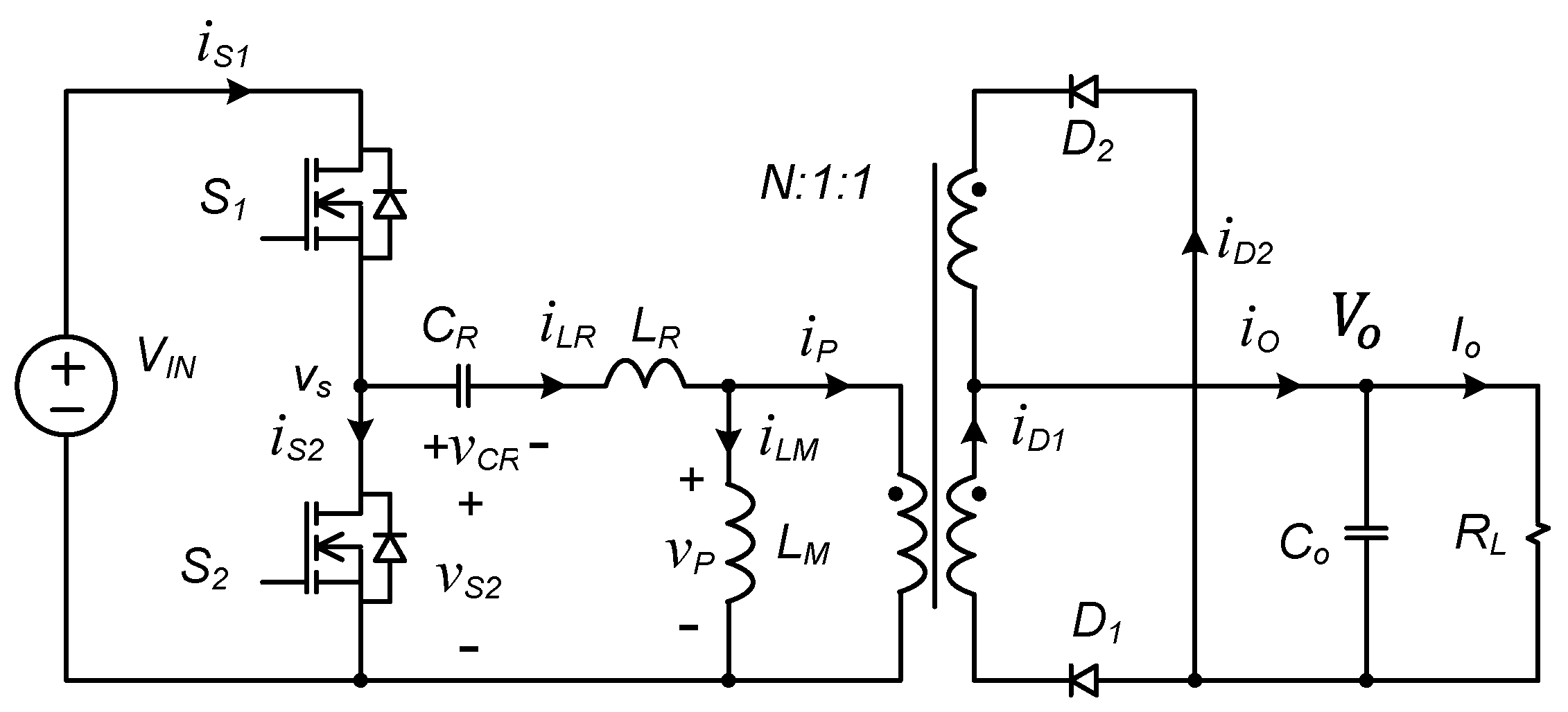
Figure 1. Basic circuit structure of half-bridge LLC resonant converter.
Energies 15 08144 g001
Figure 2. Operating waveform of LLC resonant converter in steady-state.
Energies 15 08144 g002
Figure 3. Equivalent circuit of LLC resonant converter with internal resistance.
Energies 15 08144 g003
Figure 4. Equivalent circuit for each state of the LLC resonant converter in steady-state: (a) When switch S1 is turned on; and (b) when switch S2 is turned on.
Energies 15 08144 g004
Figure 5. AC equivalent circuit of LLC resonant converter with internal loss resistance.
Energies 15 08144 g005
Figure 6. DC voltage gain M of LLC resonant converter according to each normalized frequency ω n : (a) When Q is 0; and (b) when Q is large.
Energies 15 08144 g006
Figure 7. Frequency characteristics of DC voltage gain M for LLC resonant converter according to internal loss resistance R K : (a) When the internal loss resistance R K is 0; and (b) when R K is 0.03.
Energies 15 08144 g007
Figure 8. Frequency characteristics of the DC voltage gain M.
Energies 15 08144 g008
Figure 9. The input impedance Z N of the AC equivalent circuits: (a) Equivalent circuit of input impedance Z N ; and (b) simplified equivalent circuit of input impedance Z N .
Energies 15 08144 g009
Figure 10. The frequency characteristic of the normalized input impedance Z N : (a) At Q = 0 and infinity; and (b) for various values of Q.
Energies 15 08144 g010
Figure 11. Characteristic graph of peak DC voltage gain M: (a) Peak DC voltage gain M vs. normalized frequency ω n ; (b) Q vs. Normalized frequency ω n ; (c) DC voltage gain M in accordance with internal loss resistance R K ; and (d) DC voltage gain M in accordance with inductance ratio K L .
Energies 15 08144 g011aEnergies 15 08144 g011b
Figure 12. Operating range of LLC converter.
Energies 15 08144 g012
Figure 13. Internal loss resistance and change in Q value.
Energies 15 08144 g013
Figure 14. PSIM simulation schematic of a half-bridge LLC resonant converter.
Energies 15 08144 g014
Figure 15. Steady-state waveform result of half-bridge LLC resonant converter with PSIM simulation: (a) At low load power; and (b) at full load power.
Energies 15 08144 g015
Figure 16. Basic schematic for experimental circuit.
Energies 15 08144 g016
Figure 17. Experimental circuit and experimental configuration.
Energies 15 08144 g017
Figure 18. Experimental waveform in steady-state: (a) At an input voltage of 390 V and load current of 4 A; (b) at an input voltage of 390 V and load current of 36 A; (c) at an input voltage of 400 V and load current of 4 A; and (d) at an input voltage of 400 V and load current of 36 A.
Energies 15 08144 g018
Figure 19. Frequency characteristics of DC voltage gain M at low load current: (a) Input voltage characteristics in accordance with switching frequency variation; and (b) DC voltage gain M characteristic in accordance with normalized frequency variation.
Energies 15 08144 g019
Figure 20. Frequency characteristics of DC voltage gain M at high load current: (a) Input voltage characteristics in accordance with switching frequency variation; and (b) DC voltage gain M characteristic in accordance with normalized frequency variation.
Energies 15 08144 g020
Figure 21. Load characteristics of switching frequency: (a) Input voltage of 390 V; and (b) input voltage of 400 V.
Energies 15 08144 g021
Figure 22. Measured power conversion efficiency of the experimental circuit.
Energies 15 08144 g022
Table 1. DC voltage gain M of converter according to each normalized frequency ω n .
Conditions
Q = 0
Q =
ω n = 0
M = 0
M = 0
ω n = 1 K L + 1
M =
-
ω n = 1
M = R K K L 2 + 1  
M = 1 + R K K L 2   2 Q R K + 1
ω n =
M = K L K L + 1
M = 0
Table 2. Normalized input impedance Z N of the converter, according to each normalized frequency ω n .
Conditions
Q = 0
Q =
ω n = 0
Z N =  
Z N =
ω n = 1 K L + 1
Z N = 2 R K
Z N = R K 2 + K L 2 1 + K L
ω n = 1
Z N = 4 R K 2 + K L 2
Z N = 2 R K
ω n =
Z N =  
Z N =  
Table 3. Design Conditions for LLC Resonant Converters.
ParameterSymbolValueUnit
Input voltage range V I N 360–400V
Nominal input voltage V I N   n o m 380V
Output voltage V o 54V
Maximum output power P o   m a x 2.0kW
Maximum output current I o   m a x 36A
Resonant frequency f o 125kHz
Inductance ratio K L 8-
Table 4. Main components and electrical ratings used in the experimental circuit.
ParameterSymbolValueSpecifications
Main switch S 1 , 2 SiHG73N60E650 V, 73 A, 39 mΩ
Resonant capacitor C R 2 34   nF 39   nF × 6
Resonant inductor L R 7   μ H PQ3535
Resonant inductor L M 58 μ H PQ3535
Transformer turns ratio N 35:10:10PQ3552
Rectifier switch D 1 , 2 IPP051N15N5150 V, 120 A, 5.1 mΩ
Output capacitor C o 960 μ F 120 μ F × 8
Publisher’s Note: MDPI stays neutral with regard to jurisdictional claims in published maps and institutional affiliations.