Article

Dynamic-State Analysis of Inverter Based on Cascode GaN HEMTs for PV Application

1
School of Automation, Beijing Information Science and Technology University, Beijing 100192, China
2
School of Electrical Engineering, Beijing Jiaotong University, Beijing 100044, China
3
School of Electrical Engineering, North China University of Technology, Beijing 100144, China
*
Author to whom correspondence should be addressed.
Energies 2022, 15(20), 7791; https://doi.org/10.3390/en15207791
Submission received: 24 August 2022 / Revised: 23 September 2022 / Accepted: 19 October 2022 / Published: 21 October 2022

Abstract

:
With the increase in renewable energy generation, microgrid has put forward higher requirements on the power density and performance of the photovoltaic inverter. In this paper, the dynamic process of inverter based on the cascode Gallium nitride (GaN) high electron mobility transistor (HEMT) for the photovoltaic (PV) application is analyzed in detail. The parasitic inductors and capacitors have been considered in our proposed equivalent model, which can explain the phenomenon that the crossover time of the voltage and current is prolonged by the parasitic parameters. The influence of the parasitic parameters is identified through theoretical analysis. By analyzing the influence of parasitic parameters, the design process of high-frequency inverter can be optimized. A 500 W inverter based on the cascode GaN HEMT is built, and the correctness of theoretical and simulation analysis is verified by the experimental results.

1. Introduction

The development of microgrids presents the trend of high efficiency and high power density, especially with the increase of renewable energy power generation [1,2]. Nowadays, single-phase photovoltaic (PV) inverters have been widely applied, especially in the Microgrid background. Unlike conventional PV inverters, single-phase PV inverters will most likely reach a high level of efficiency at a low cost, for the single-stage structure without a transformer [3,4]. However, traditional single-phase PV inverters suffer from low power density because of large passive components. The passive components, such as the inductors, have critical effects on the efficiency, performance, and cost of PV inverters [5,6]. Moreover, the switching loss of the power devices has been a bottleneck for further improvements in power density and efficiency. One key issue of high-power density must be solved by increasing the switching frequency. Since the switching frequency of the Si-based inverter normally is limited up to 20 kHz~30 kHz, the passive components are always large so as to reduce the switching loss, which decreases the power density.
The traditional power devices based on Si materials have basically reached their theoretical limits and gradually cannot meet the stringent requirements of the microgrid [7,8,9,10]. The emergence of the wide-bandgap device has changed the existing structure of the semiconductor industry and opened a new situation for the semiconductor industry [11,12]. Wide bandgap semiconductors have become ideal substitutes for power converters [13,14,15]. GaN HEMT devices have excellent electrical and physical properties and huge market potential [16,17]. It has been widely concerned and has been applied in many fields, including DC/AC GaN HEMT-based inverters [18,19], AC/DC GaN HEMT-based PFC circuits [20,21], and DC/DC GaN HEMT-based converters [22,23,24], etc.
Parasitic inductance is an important parameter of the power device, which has an important influence on the dynamic characteristics of power devices. The most critical parasitic parameter affecting the dynamic performance of devices is the common source inductance (CSI) [25,26]. CSI is defined as the inductance shared by the main power and drive circuit. Recently, the research on parasitic parameters of SiC and GaN HEMT mainly focuses on enhancement types, which are all single switch structures. Their conclusions are similar to those of Si MOSFETs [27]. Because of the special structure of cascode GaN HEMT, its dynamic characteristics are more complex than the enhancement device. At the same time, it is more easily affected by the CSI. Therefore, the dynamic process analysis of cascode GaN HEMT also needs to be analyzed, especially in the application of a high-frequency inverter.
On the other hand, the turn-on and turn-off speed of GaN HEMT devices is significantly higher than that of silicon devices. And the turn-on rate of current can reach 3000 A/us, so the oscillation of voltage and current is easy to occur, especially in the bridge structure [28,29,30,31]. In high-power applications, the bridge circuit is one of the most widely used topologies, so the dynamic-state analysis of GaN HEMT in bridge structure needs to be solved urgently [31,32,33]. The dynamic-state operation mode of the cascode GaN HEMT and its application are important areas that need further research [34,35,36,37,38]. In [4,5], a third-quadrant operation mode of the enhancement GaN HEMT was demonstrated. However, the mechanism of the cascode GaN HEMT is different from either Si MOSFET or enhancement GaN HEMT. The device characteristics of Cascode GaN HEMT are analyzed in reference [34,35]. Based on the buck circuit, the switching process of cascode GaN HEMT is analyzed and modeled, and an accurate mathematical model is obtained, which provides theoretical support for loss analysis. At the same time, the mathematical model is used to optimize the simulation model to make the simulation model match the experimental results well. The results of this paper are of great significance to the application and loss analysis of GaN HEMT. However, the performance of the freewheeling diode has a great influence on the double pulse test results. Further, the freewheeling diode used is the GaN Schottky diode which has been discontinued by Transphrom Corporation for some reason and cannot be purchased from the market at present. Therefore, in practical applications, users can only select part of the test results for reference. The switching characteristics of cascode GaN HEMT and GaN diodes of 600 V/20 A are tested in reference [36]. On this basis, the mathematical model of GaN HEMT switching loss and reverse recovery charge is given. However, this paper uses a sampling resistor to measure the current, leading to serious distortion of the measured current. The drain current oscillates seriously at turn-on time, which is different from the real situation. The switching characteristics of the cascode GaN HEMT were tested in reference [37,38]. In this paper, the reason for bridge circuit oscillation is analyzed, which provides an important idea for the application of GaN HEMT bridge circuit. However, the layout of the switches is not clear, and the parasitic parameters of the main power layout were not given, so the accuracy of the waveform cannot be ensured.
Cascode GaN HEMT is a typical device for high voltage application of wide-bandgap devices. Its special structure makes the working process of the device more complex than that of traditional Si MOSFET and the enhancement of GaN HEMT. In this paper, a 600 V cascode GaN HEMT-based inverter for PV application is evaluated. Based on the working process analysis of cascode GaN HEMT, the dynamic process analysis of cascode GaN HEMT based single-phase inverter circuit is presented. In addition, the influence of parasitic parameters is considered in the model, and the key equations of each mode are obtained. Further, the influence of parasitic parameters on the switching process of the switch is discussed. Finally, a 500 W cascode GaN HEMT-based single-phase inverter is established, and experiment results verify the correctness of theoretical and simulation analysis.

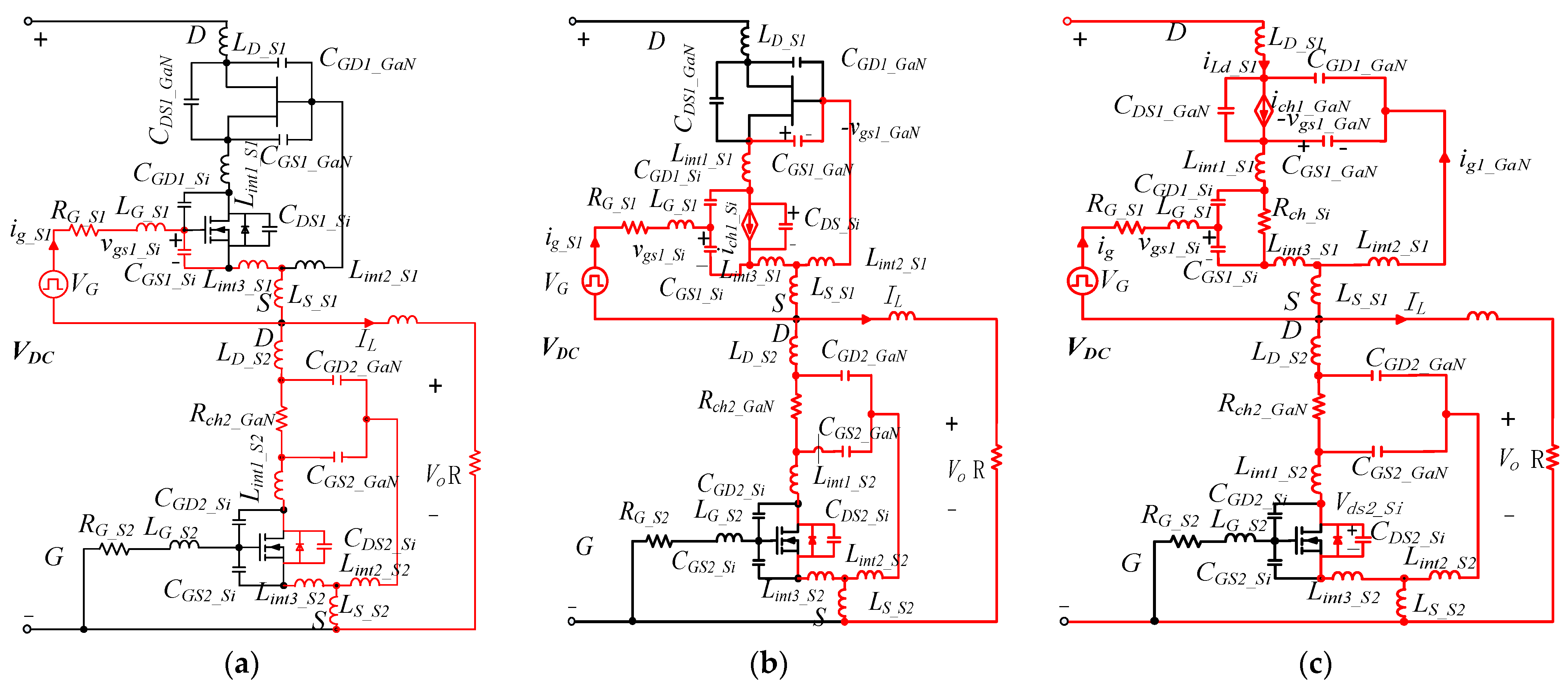
2. Characteristic and Model of Cascode GaN HEMT

Cascode GaN HEMT comprises low voltage enhanced silicon MOSFET and high voltage depletion GaN HEMT. The internal structure is shown in Figure 1a, and the equivalent diagram considering parasitic inductors and capacitors is shown in Figure 1b [4], in which the red loop represents the drive circuit of the Si MOSFET, the bule loop represents the main power loop and the green loop represents the drive loop of GaN HEMT. Because of the complex structure of cascode GaN HEMT, its parasitic parameters are more than that of E-mode GaN HEMT. It includes the parasitic capacitance and inductance in the device and the parasitic inductance in the main power circuit and drive circuit. The parasitic capacitance in the device includes gate-source parasitic capacitance CGS_Si, gate-drain parasitic capacitance CGD_Si, drain-source parasitic capacitance CDS_Si of the low voltage Si MOSFET and Gate-source parasitic capacitance CGS_GaN, gate-drain parasitic capacitance CGD_GaN and drain-source parasitic capacitance CDS_GaN of high voltage depletion GaN HEMT. The parasitic inductors in the device include Lint1, Lint2, Lint3, and LS, LG, and LD on the pins. It can be seen that for Si MOSFET, Lint3 and LS are shared by the Si MOSFET drive circuit and main power circuit, so Lint3 and LS are common source inductors of Si MOSFET. Similarly, for GaN HEMT, the blue loop is still the main power loop, while the drive loop of GaN HEMT is the green loop. Therefore, the common source inductances of GaN HEMT are Lint3 and Lint1. Lint3 is the common source inductor of GaN HEMT and Si MOSFET, so Lint3 is the most critical parasitic inductor. The common source inductor of high-voltage GaN HEMT is Lint1, which affects the main loss of the switch, and is the second key parasitic inductance. LS is the third most critical parasitic inductance. Among them, Lint1, Lint2, and Lint3 are parasitic parameters inside the device which cannot be tested and changed. Therefore, this paper only considered the effect of LS in the experiment section.

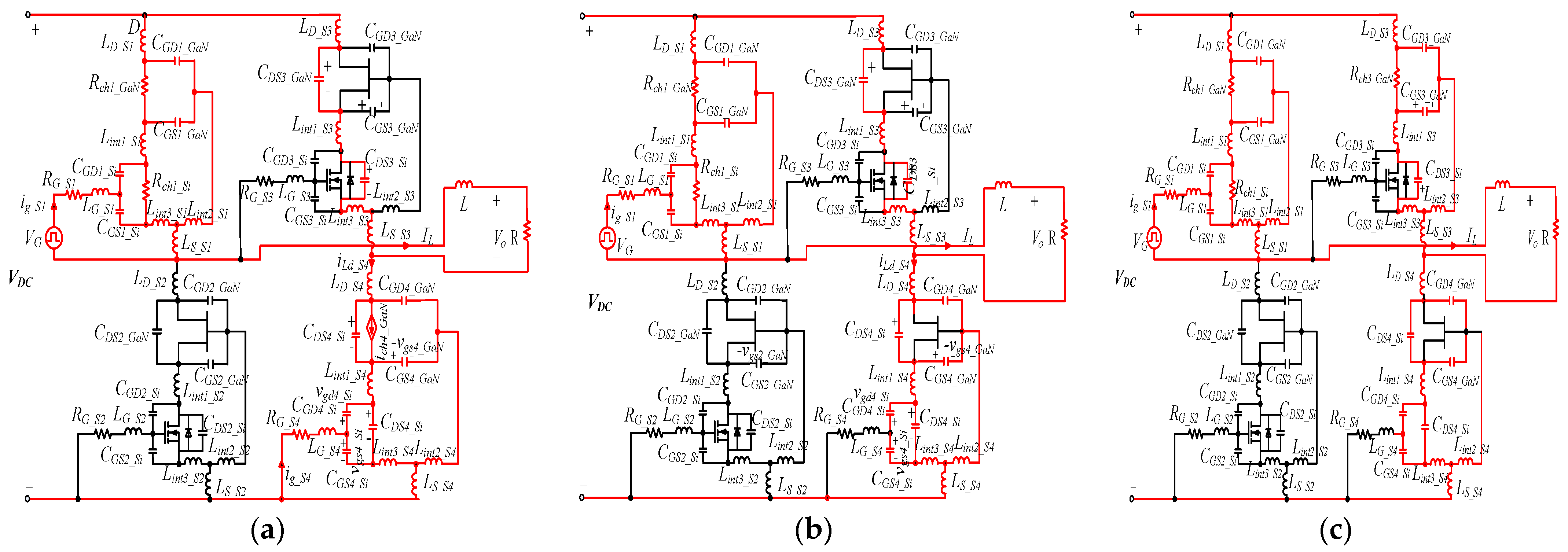
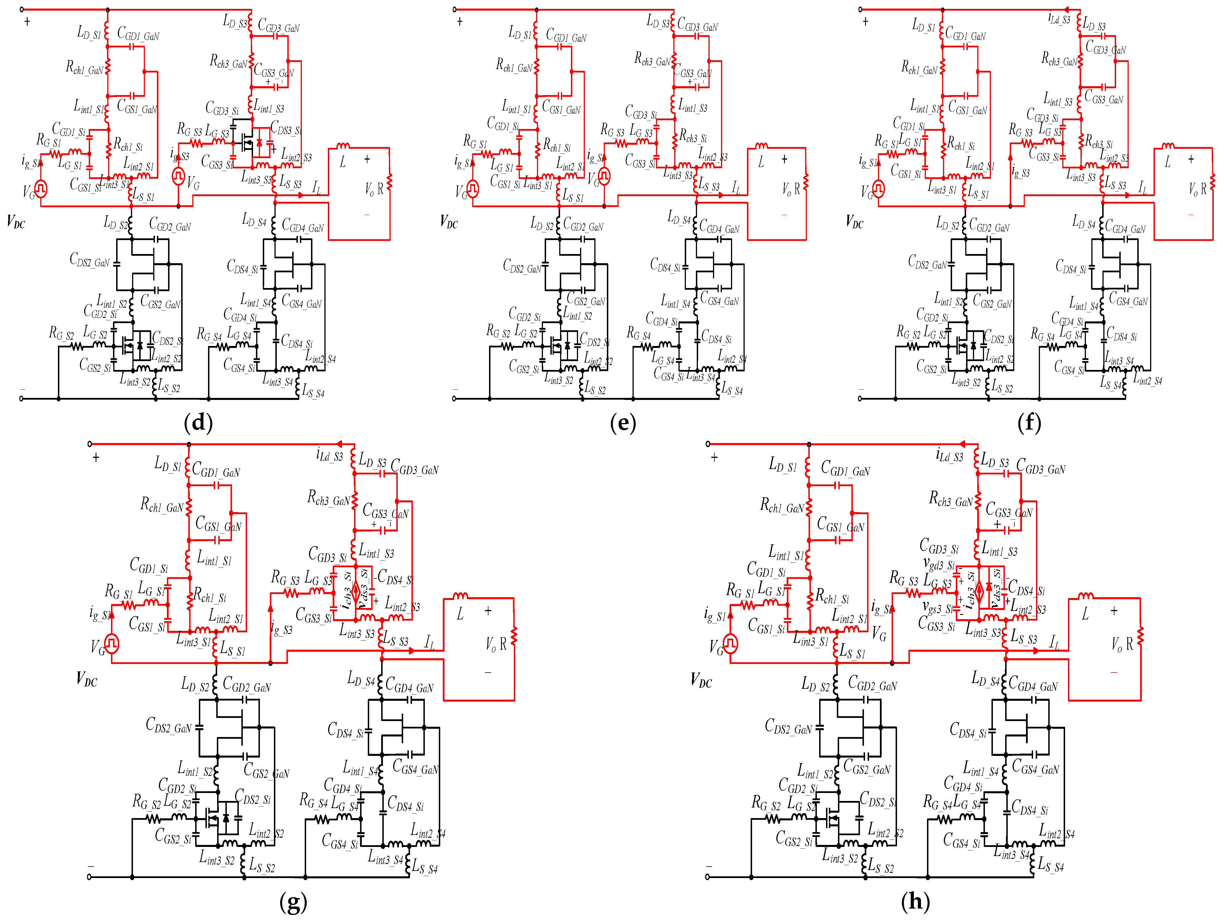
3. Dynamic Analysis of Inverter Based on Cascode GAN HEMT

The cascode GaN HEMT is applied in a single-phase full bridge inverter, and the unipolar SPWM control strategy is adopted, as shown in Figure 2a,b, respectively. The dynamic-state analysis of the cascode GaN HEMT can be distinguished as follows:

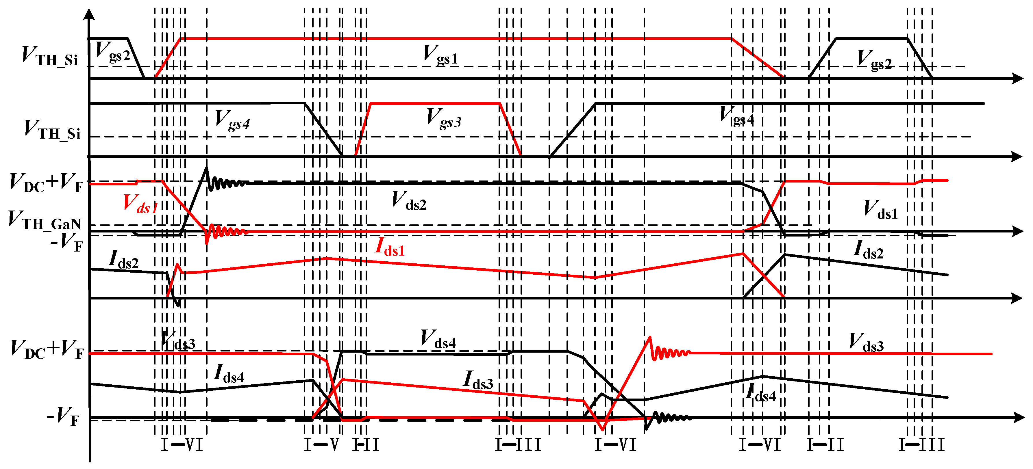
3.1. Positive Turn-On Process of the Bridge Leg Switches

Before S1 turns on, The vgs_S2 = 0 and vgs_S4 = VG, and the current is positive, as shown in Figure 2b. The inductance IL current conducts through S2 and S4. The positive turn-on process of cascode GaN HEMT is analyzed as follows.
Stage I: CGS1_Si charged state.
When the gate voltage VG is applied on S1, the gate-source equivalent capacitance CGS_Si is charged. As S1 is turned off, current IL keeps flowing through S2 and S4. This stage ends when vgs1_Si = VTH_Si. From Figure 3a, the following equations can be obtained:
{ i g _ S 1 = C G S 1 _ S i d v g s 1 _ S i d t V G = ( L G _ S 1 + L i n t 3 _ S 1 + L S _ S 1 ) d i g _ S 1 d t + R G _ S 1 i g _ S 1 + v g s 1 _ S i
Stage II: Si MOSFET drain-source voltage vds1_Si of S1 falling stage.
When vgs_S1 is equal to VTH_Si, Si MOSFET of S1 begins conducting. At this point, CGD_Si, CDS_Si, and CGS_GaN begin to discharge through the channel of Si MOSFET. This stage continues until vgs_GaN = VTH_GaN. The equivalent circuit of this stage is shown in Figure 3b. The formula for this stage is shown in Equation (2).
{ V G = ( L G _ S 1 + L i n t 3 _ S 1 + L S _ S 1 ) d i g _ S 1 d t + R G _ S 1 i g _ S 1 + v g s 1 _ S i i g _ S 1 = C G S 1 _ S i d v g s 1 _ S i d t + C G D 1 _ S i d ( v g s 1 _ S i v d s 1 _ S i ) d t g m 1 _ s i ( v g s 1 _ S i V T H _ S i ) = C G D 1 _ S i d ( v g s 1 _ S i v d s 1 _ S i ) d t ( C D S 1 _ S i + C G S 1 _ G a N ) d v d s 1 _ S i d t
Stage III: ich1_GaN of S1 rising stage.
When vgs1_GaN reaches VTH_GaN, the channel of S1 starts to turn on and equivalent capacitors CDS1_GaN and CGD1_GaN start discharging through the channel of GaN HEMT. It causes vds1_GaN to fall. As S2 still conducts, the voltage difference between Vdc and vds1_GaN forces the load current iL to increase. The equivalent circuit of this stage is shown in Figure 3c. Then, Equation (3) could be derived.
Stage IV: S2 MOSFET reverse recovery stage.
When the iLd_S1 reaches IL, the reverse recovery of S2 begins. The equivalent circuit and equations are the same as stage III.
Stage V: S2 GaN HEMT turns off stage.
When the reverse recovery is complete, the voltage vds_S1 rises since the vds_S1 < −VTH_GaN, the GaN HEMT channel of S2 turns on. When vds_S2 = VTH_GaN, this stage ends. The equivalent circuit of this stage is shown in Figure 3d. Then, Equation (4) could be derived.
Stage VI: drain-source voltage of S2 rising stage.
When vds_S2 = VTH_GaN, the GaN HEMT channel of S2 turns off, the equivalent capacitance is charged, and the voltage vds_S2 rises until the voltage vds_S1 decreases to zero, as shown in Figure 3e. Then, Equation (5) could be derived.
{ v g s 1 _ G a N + ( L i n t 1 _ S 1 + L i n t 2 _ S 1 + L i n t 3 _ S 1 ) d i g 1 _ G a N d t + ( L i n t 1 _ S 1 + L i n t 3 _ S 1 ) d i L d _ S 1 d t + R c h 1 _ S i ( i g 1 _ G a N + i L d _ S 1 ) = 0 i g 1 _ G a N = C G S 1 _ G a N d v g s 1 _ G a N d t + C G D 1 _ G a N d ( v g s 1 _ G a N v d s 1 _ G a N ) d t g m 1 _ G a N ( v g s 1 _ G a N V T H _ G a N ) = C G D 1 _ G a N d ( v g s 1 _ G a N v d s 1 _ G a N ) d t + C D S 1 _ G a N d v d s 1 _ G a N d t + i L d _ S 1 V d c = ( L D _ S 1 + L S _ S 1 + L i n t 1 _ S 1 + L i n t 3 _ S 1 ) d i L d _ S 1 d t + ( L i n t 1 _ S 1 + L i n t 3 _ S 1 ) d i g 1 _ G a N d t + v d s 1 _ G a N + R c h 1 _ S i ( i g 1 _ G a N + i L d _ S 1 )
{ V d c = ( L D _ S 1 + L S _ S 1 + L i n t 1 _ S 1 + L i n t 3 _ S 1 ) d i L d _ S 1 d t + ( L i n t 1 _ S 1 + L i n t 3 _ S 1 ) d i g 1 _ G a N d t + C d s 2 _ S i R c h 2 _ G a N d v d s 2 _ S i d t + v d s 1 _ G a N + R c h 1 _ S i ( i g 1 _ G a N + i L d _ S 1 ) + v d s 2 _ S i i L d 1 = I L + C d s 2 _ S i d v d s 2 _ S i d t
{ i L d _ S 1 = I L + ( C D S 2 _ S i + C D S 2 _ G a N ) d v d s 2 d t V d c = ( L D _ S 1 + L S _ S 1 + L i n t 1 _ S 1 + L i n t 3 _ S 1 ) d i L d _ S 1 d t + ( L i n t 1 _ S 1 + L i n t 3 _ S 1 ) d i g 1 _ G a N d t + v d s 1 _ G a N + R c h 1 _ S i ( i g _ G a N + i L d ) + v d s 2

3.2. Positive Turn-off Process of the Bridge Leg Switches

Before S4 turns off, vgs_S1 = vgs_S4 = VG, and the current is positive. The positive turn-off process of S4 is analyzed as follows.
Stage I: CGS4_Si discharged stage.
As the gate voltage VG of S4 falls to zero, the equivalent capacitor CGS4_Si of S4 is discharged. The equivalent circuit of this stage is shown in Figure 3f. When the Si MOSFET enters the amplification region and satisfies the requirements of GSi (vgs_SiVTH_Si) = IL, this stage ends. The key formula for this stage is shown in Equation (6).
{ i g _ S 4 = ( C G S 4 _ S i + C G D 4 _ S i ) d v g s 4 _ S i / d t ( L G _ S 4 + L S _ S 4 ) d i g _ S 4 / d t + R G _ S 4 i g _ S 4 + v g s 4 _ S i = 0
Stage II: vds4_Si of S4 rising stage.
As vgs4_Si continues to decrease, the channel current of Si MOSFET is controlled by transfer characteristics, which is less than IL. The excess current charges the drain-source equivalent capacitors, and vds4_Si increases. Because CDS4_Si is in parallel with CGS4_GaN, vgs4_GaN decreases. The equivalent circuit of this stage is shown in Figure 3g, and the key formula for this stage is shown in Equation (7). This stage ends when the GaN HEMT of S4 enters the saturation region.
Stage III: Channel current of S4 decreasing stage.
As the GaN HEMT gate-source voltage of S4 continues to decrease, the GaN HEMT channel saturation current of S4 is less than IL. The excess current charges drain-source equivalent capacitors and vds4_GaN increases. This stage ends when the channel of depletion GaN HEMT is completely closed, as shown in Figure 4a. The key formula for this stage is shown in Equation (8).
Stage IV: The drain-source voltage of the S4 rising stage.
After the vgs4_GaN dropping below the threshold value of GaN HEMT, S4 totally turns off. The junction capacitors of S4 are charged by iLD_S4, then the drain-source voltage of S4 increases, as shown in Figure 4b. This stage ends when the drain-source voltage of S3 falls to a threshold value of GaN HEMT. The formula for this stage is shown in Equation (9).
Stage V: The GaN HEMT channel of the S3 conducting stage.
After the drain-source voltage of S3 is smaller than the threshold value of GaN HEMT, the GaN HEMT channel of S3 turns on. The drain-source voltage of S3 continues to reduce. This stage ends when the MOSFET body diode of S3 is forward-biased. Thus, inductor current flows through S3, as shown in Figure 4c, and the formula is the same as stage IV.
{ ( L G _ S 4 + L S _ S 4 ) d i g _ S 4 / d t + R G _ S 4 i g _ S 4 + v g s 4 _ S i = 0 i g _ S 4 = C G S 4 _ S i d v g s 4 _ S i / d t + C G D 4 _ S i d ( v g s 4 _ S i + v d s 4 _ S i ) / d t g m 4 _ S i ( v g s 4 _ S i V T H _ S i ) = C G D 4 _ S i d ( v g s 4 _ S i v d s 4 _ S i ) d t ( C D S 4 _ S i + C G S 4 _ G a N ) d v d s 4 _ S i d t + I L
{ i L d _ S 4 = I L + ( C D S 3 _ G a N + C D S 3 _ S i ) d v d s _ S 3 / d t ( L D _ S 4 + L S _ S 4 + L i n t 1 _ S 4 + L i n t 3 _ S 4 ) d i L d _ S 4 / d t + v d s 4 _ G a N v g s 4 _ G a N + v d s _ S 3 = V d c i L d _ S 4 = ( C G S 4 _ G a N + C D S 4 _ S i + C G D 4 _ S i ) d v g s 4 _ G a N / d t C G D 4 _ G a N d ( v g s 4 _ G a N v d s 4 _ G a N ) / d t g m 4 _ G a N ( v g s 4 _ G a N V T H _ G a N ) = C G D 4 _ G a N d ( v g s 4 _ G a N v d s 4 _ G a N ) / d t C D S 4 _ G a N d v d s 4 _ G a N / d t + i L d _ S 4
{ ( C G S 4 _ G a N + C D S 4 _ S i + C G D 4 _ S i / / C G S 4 _ S i ) d v d s 4 _ S i / d t = C D S 4 _ G a N d v d s 4 _ G a N / d t i L d _ S 4 = C G D 4 _ G a N d ( v d s 4 _ G a N + v d s 4 _ S i ) / d t + C D S 4 _ G a N d v d s 4 _ G a N / d t

3.3. Reverse Turn-on Process of the Bridge Leg Switches

Before vgs_S3 = VG, the vgs_S1 = VG. The current is positive, flowing through S1 and S3. The reverse turn-on process is analyzed as follows.
Stage I: CGS3_Si charged stage.
This stage is the same as the CGS1_Si charged period, as shown in Figure 4d. Then, the equations could be derived as follow.
{ V G = ( L G _ S 3 + L i n t 3 _ S 3 + L S _ S 3 ) d i g _ S 3 / d t + R G _ S 3 i g _ S 3 + v g s 3 _ S i i g _ S 3 = C G S 3 _ S i d v g s 3 _ S i / d t
Stage II: the MOSFET channel of S3 conducting stage.
Since S3 is in the freewheeling state, the GaN HEMT of S3 is totally turned on. When the vgs_S3 > VTH_Si, the channel of S3 is totally turned on. IL transfers from MOSFET’s body diode to the MOSFET’s channel, as shown in Figure 4e.

3.4. Reverse Turn-Off Process of the Bridge Leg Switches

Before vgs_S3 = 0, the vgs_S1 = vgs_S3 = VG. The current is positive, flowing through S1 and S3. The channel turning off transition of S3 can be divided into three stages as follow:
Stage I: CGS3_Si discharged stage.
This stage is the same as the CGS4_Si discharged state, as shown in Figure 4f. Then, Equation (11) could be derived.
{ ( L G _ S 3 + L S _ S 3 ) d i g _ S 3 / d t + R G _ S 3 i g _ S 3 + v g s 3 _ S i = 0 i g _ S 3 = ( C G S 3 _ S i + C G D 3 _ S i ) d v g s 3 _ S i / d t
Stage II: The vds3_Si of S3 rising stage.
This stage is the same as the vds4_Si of the S4 rising stage. This stage ends when vds4_Si rises to diode forward voltage VF, as shown in Figure 4g. Then, Equation (12) could be derived.
Stage III: MOSFET body diode of S3 conducting stage.
When vds4_Si rises to diode forward voltage VF, the MOSFET body diode of S3 is forward-biased, and the inductor current IL transfers from the MOSFET channel to the MOSFET body diode. This stage ends when the Si MOSFET channel of S3 totally shuts down, as shown in Figure 4h. Thus, Equation (13) could be calculated.
As we can see from the theoretical analysis, the parasitic parameters influence the dynamics to the state of the switching state. The main switching waveforms of the cascode GaN HEMT-based single-phase inverter is shown in Figure 5.
{ i g _ S 3 = C G S 3 _ S i d v g s 3 _ S i / d t + C G D 3 _ S i d ( v g s 3 _ S i + v d s 3 _ S i ) / d t ( L G _ S 3 + L S _ S 3 ) d i g _ S 3 / d t + R G _ S 3 i g _ S 3 + v g s 3 _ S i = 0 g m 3 _ S i ( v g s 3 _ S i V T H _ S i ) = C G D 3 _ S i d ( v g s 3 _ S i v d s 3 _ S i ) / d t ( C D S 3 _ S i + C G S 3 _ G a N ) d v d s 3 _ S i / d t + I L
{ v d s 3 _ S i = V F ( L G _ S 3 + L S _ S 3 ) d i g _ S 3 / d t + R G _ S 3 i g _ S 3 + v g s 3 _ S i = 0 i g _ S 3 = C G S 3 _ S i d v g s 3 _ S i / d t + C G D 3 _ S i d ( v g s 3 _ S i + v d s 3 _ S i ) / d t g m 3 _ S i ( v g s 3 _ S i V T H _ S i ) = C G D 3 _ S i d ( v g s 3 _ S i + v d s 3 _ S i ) / d t ( C D S 3 _ S i + C G S 3 _ G a N ) d v d s 3 _ S i / d t i D 3 _ S i + I L

4. Simulation and Experimental Verifications

The single-phase inverter circuit base on cascode GaN HEMTs is simulated and verified using LTSpice. The simulation conditions are Vin = 380 V, Vo = 220 V, Po = 500 W. The working waveforms of cascode GaN HEMT are shown in Figure 6a. In addition, the simulation results of drain-source voltage waveforms are shown in Figure 6b,c with parasitic parameters LS = 5 nH and LS = 20 nH, respectively. As we can see, the voltage spike of GaN HEMT is larger with the increase of LS.
A 500 W prototype was built to verify the performance of a cascode GaN HEMT-based single-phase inverter. The experimental waveforms are obtained. The voltage spike of GaN HEMT is larger with the increase of LS, as shown in Figure 7a,b. Finally, waveform of 500 W single-phase inverter is given under the condition that Vin = 380V, and Vo = 220V, as shown in Figure 7c. The inverter inductance current IL, and drain-source voltage vds of S1 and S4 are shown, respectively. The parasitic parameters LS should be controlled within 5nH, so as to reduce the drain-source voltage spike of the cascode GaN HEMT. The efficiency curves of the single-phase inverter base on TP65H150G4PS at different switching frequencies (20 kHz, 50 KHz, 100 kHz) are shown in Figure 7d. The switching loss increases as the switching frequency increases, and the overall efficiency of the inverter decreases. It can be seen that the maximum efficiency point is around 300 W in Figure 7d, which is a balance of the switching loss and the filter loss. When the power is low, the switching loss is dominant. With the increase of the power, the loss of the filter inductance increases and becomes dominant.

5. Conclusions

Dynamic-state process of the 600 V cascode GaN HEMT is analyzed in this paper. We apply cascode GaN HEMT in a single-phase DC/AC inverter. Lint2, Lint3, and LS are the most critical parasitic, which will significantly affect the dynamic performance of the cascode GaN HEMT. The influence of the parasitic inductance is identified through theoretical analysis and verified by simulation and experiment results. With the increase in frequency, the parasitic parameter Ls should be reduced as much as possible to reduce the influence on the drain-source voltage of the cascode GaN HEMT. Finally, a 500 W cascode GaN HEMT-based single-phase inverter is established, and the experiment results verified the correctness of theoretical and simulation analysis.

Author Contributions

Y.Z. structured the paper, reviewed major references cited, and is the main author of the paper. J.L. and J.W. contributed to the writing of relevant sections. T.Q.Z. and P.J. provided valuable comments and discussion. All authors have read and agreed to the published version of the manuscript.

Funding

This work was supported by the National Natural Science Foundation of China under Grant no.52107176 and no. 52237008, in part by the Natural Science Foundation of Beijing under Grant no. KZ201911232045, in part by the National Natural Science Foundation of China under Grant no.51907002, in part by the Talent Fund of Beijing Jiaotong University under Grant 2022XKRC011.

Conflicts of Interest

The authors declare no conflict of interest.

References

  1. Bai, F.; Cui, Y.; Yan, R.; Saha, T.K.; Gu, H.; Eghbal, D. Frequency Response of PV Inverters Toward High Renewable Penetrated Distribution Networks. CSEE J. Power Energy Syst. 2022, 8, 465–475. [Google Scholar]
  2. Gu, H.J.; Yan, R.F.; Saha, T.K. Review of system strength and inertia requirements for the national electricity market of Australia. CSEE J. Power Energy Syst. 2019, 5, 295–305. [Google Scholar]
  3. Alajmi, B.N.; Ahmed, K.H.; Adam, G.P.; Williams, B.W. Single-Phase Single-Stage Transformer less Grid-Connected PV System. IEEE Trans. Power Electron. 2012, 28, 2664–2676. [Google Scholar] [CrossRef]
  4. Barater, D.; Lorenzani, E.; Concari, C.; Franceschini, G.; Buticchi, G. Recent advances in single-phase transformerless photovoltaic inverters. IET Renew. Power Gener. 2016, 10, 260–273. [Google Scholar] [CrossRef]
  5. Freddy, T.K.S.; Rahim, N.A.; Hew, W.-P.; Che, H.S. Comparison and Analysis of Single-Phase Transformerless Grid-Connected PV Inverters. IEEE Trans. Power Electron. 2013, 29, 5358–5369. [Google Scholar] [CrossRef]
  6. Son, G.; Huang, Z.; Li, Q.; Lee, F.C. Analysis and Control of Critical Conduction Mode High-Frequency Single-Phase Transformerless PV Inverter. IEEE Trans. Power Electron. 2021, 36, 13188–13199. [Google Scholar] [CrossRef]
  7. Lidow, A.; Strydom, J.; de Rooij, M.; Ma, Y. GaN Transistorsfor Efficient Power Conversion; Power Conversion Publications: El Seguno, CA, USA, 2012. [Google Scholar]
  8. Boutros, K.S.; Chu, R.; Hughes, B. GaN power electronics for automotive application. In Proceedings of the IEEE Energytech, 2012, Cleveland, OH, USA, 29–31 May 2012; pp. 1–4. [Google Scholar]
  9. Morita, T.; Tamura, S.; Anda, Y.; Ishida, M.; Uemoto, Y.; Ueda, T.; Tanaka, T.; Ueda, D. 99.3% Efficiency of three-phase inverter for motor drive using GaN-based Gate injection transistors. In Proceedings of the 2011 Twenty-Sixth Annual IEEE Applied Power Electronics Conference and Exposition (APEC), Fort Worth, TX, USA, 6–11 March 2011; pp. 481–484. [Google Scholar]
  10. Tamura, S.; Anda, Y.; Ishida, M.; Uemoto, Y.; Ueda, T.; Tanaka, T.; Ueda, D. Recent advances in gan power switching devices. In Proceedings of the 2010 IEEE Compound Semiconductor Integrated Circuit Symposium (CSICS), Monterey, CA, USA, 3–6 October 2010; pp. 1–4. [Google Scholar]
  11. Zhao, C.; Trento, B.; Jiang, L.; Jones, E.A.; Liu, B.; Zhang, Z.; Costinett, D.; Wang, F.F.; Tolbert, L.M.; Jansen, J.F.; et al. Design and implementation of a gan-based, 100-khz, 102-w/in3 single-phase inverter. IEEE J. Emerg. Sel. Top. Power Electron. 2016, 4, 824–840. [Google Scholar] [CrossRef]
  12. Wang, K.; Yang, X.; Wang, L.; Jain, P. Instability Analysis and Oscillation Suppression of Enhancement-Mode GaN Devices in Half-Bridge Circuits. IEEE Trans. Power Electron. 2017, 33, 1585–1596. [Google Scholar]
  13. Zhang, Y.; Li, J.; Wang, J. Investigations on Driver and Layout for Paralleled GaN HEMTs in Low Voltage Application. IEEE Access 2019, 7, 179134–179142. [Google Scholar] [CrossRef]
  14. Jones, E.A.; Wang, F.F.; Costinett, D. Review of Commercial GaN Power Devices and GaN-Based Converter Design Challenges. IEEE J. Emerg. Sel. Top. Power Electron. 2016, 4, 707–719. [Google Scholar] [CrossRef]
  15. Mu, M.; Lee, F.C. Design and Optimization of a 380–12V High-Frequency, High-Current LLC Converter with GaN Devices and Planar Matrix Transformers. IEEE J. Emerg. Sel. Top. Power Electron. 2016, 4, 854–862. [Google Scholar]
  16. Liu, Z.; Lee, F.C.; Li, Q.; Yang, Y. Design of GaN-based MHz totem-Pole PFC rectifier. IEEE J. Emerg. Sel. Top. Power Electron. 2016, 4, 799–807. [Google Scholar] [CrossRef]
  17. Huang, X.; Lee, F.C.; Li, Q.; Du, W. High-Frequency high-efficiency GaN-based interleaved crm bidirectional buck/boost converter with inverse coupled inductor. IEEE Trans. Power Electron. 2016, 31, 4343–4352. [Google Scholar] [CrossRef]
  18. Zhang, L.; Born, R.; Zhao, X.; Lai, J.S. A high efficiency inverter design for Google little box challenge. In Proceedings of the 2015 IEEE 3rd Workshop on Wide Bandgap Power Devices and Applications (WiPDA), Blacksburg, VA, USA, 2–4 November 2015; pp. 319–322. [Google Scholar]
  19. Morsy, A.S.; Bayern, M.; Enjeti, P. High power density single-phase inverter using GaN FETS and active power decoupling for Google little box challenge. In Proceedings of the 2015 IEEE 3rd Workshop on Wide Bandgap Power Devices and Applications (WiPDA), Blacksburg, VA, USA, 2–4 November 2015; pp. 323–327. [Google Scholar]
  20. Liu, Z.; Huang, X.; Mu, M.; Yang, Y.; Lee, F.C.; Li, Q. Design and evaluation of GaN-based dual-phase interleaved MHz critical mode PFC converter. In Proceedings of the 2014 IEEE Energy Conversion Congress and Exposition (ECCE), Pittsburgh, PA, USA, 14–18 September 2014; pp. 611–616. [Google Scholar]
  21. Zhang, X.; Yao, C.; Lu, X.; Davidson, E.; Sievers, M.; Scott, M.J.; Xu, P.; Wang, J. A GaN transistor based 90W AC/DC adapter with a buck-PFC stage and an isolated Quasi-switched-capacitor DC/DC stage. In Proceedings of the 2014 IEEE Applied Power Electronics Conference and Exposition, Fort Worth, TX, USA, 16–20 March 2014. [Google Scholar]
  22. Zhao, X.; Yeh, C.S.; Zhang, L.; Lai, J.S.; Labella, T. A 2-MHz wide-input hybrid resonant converter with ultra-compact planar coupled inductor for low power integrated on-chip applications. IEEE Trans. Ind. Appl. 2018, 54, 376–387. [Google Scholar] [CrossRef]
  23. Jenkins, L.L.; Wilson, C.G.; Moses, J.D.; Aggas, J.M.; Rhea, B.K.; Dean, R.N. The impact of parallel GaN HEMTs on efficiency of a 12-to-1 V buck converter. In Proceedings of the 2013 IEEE Workshop on Wide Bandgap Power Devices and Applications (WiPDA), Columbus, OH, USA, 27–29 October 2013; pp. 197–200. [Google Scholar]
  24. Wu, Y.F. Paralleling high-speed GaN power HEMTs for quadrupled power output. In Proceedings of the Twenty-Eighth Annual IEEE Applied Power Electronics Conference and Exposition (APEC), Long Beach, CA, USA, 17–21 March 2013; pp. 211–214. [Google Scholar]
  25. Zhu, T.; Zhuo, F.; Zhao, F.; Wang, F.; Zhao, T. Quantitative Model-Based False Turn-on Evaluation and Suppression for Cascode GaN Devices in Half-Bridge Applications. IEEE Trans. Power Electron. 2019, 34, 10166–10179. [Google Scholar] [CrossRef]
  26. Zhao, F.; Li, Y.; Chen, Z.; Yang, S.; Chen, J. Negative Conductance Modeling and Stability Analysis of High-frequency Oscillation Based on Cascode GaN Circuits. IEEE Access 2020, 8, 114100–114111. [Google Scholar] [CrossRef]
  27. Lu, J.; Bai, H.; Brown, A.; McAmmond, M.; Chen, D.; Styles, J. Design consideration of gate driver circuits and PCB parasitic parameters of paralleled E-mode GaN HEMTs in zero-voltage-switching applications. In Proceedings of the 2016 IEEE Applied Power Electronics Conference and Exposition (APEC), Long Beach, CA, USA, 20–24 March 2016; pp. 529–535. [Google Scholar]
  28. Yajing, Z.; Jiuhe, W.; Hong, L.; Lijie, W.; Yan, L.; Zheng, T.Q. The drive circuit design for paralleling operation of enhancement GaN HEMT in an isolated DC-DC converter. In Proceedings of the 2018 IEEE Workshop on Wide Bandgap Power Devices and Applications (WiPDA), Xi’an, China, 16–18 May 2018. [Google Scholar]
  29. Li, H.; Munk-Nielsen, S.; Wang, X.; Maheshwari, R.; Beczkowski, S.; Uhrenfeldt, C.; Franke, W.-T. Influences of Device and Circuit Mismatches on Paralleling Silicon Carbide MOSFETs. IEEE Trans. Power Electron. 2015, 31, 621–634. [Google Scholar] [CrossRef] [Green Version]
  30. Pajnić, M.; Pejović, P.; Despotović, Ž.; Lazić, M.; Skender, M. Characterization and gate drive design of high voltage cascode GaN HEMT. In Proceedings of the 2017 International Symposium on Power Electronics (Ee), Novi Sad, Serbia, 19–21 October 2017; pp. 1–5. [Google Scholar]
  31. Efthymiou, L.; Camuso, G.; Longobardi, G.; Chien, T.; Chen, M.; Udrea, F. On the source of oscillatory behavior during switching of power enhancement mode GaN HEMTs. Energies 2017, 10, 407. [Google Scholar] [CrossRef] [Green Version]
  32. Chen, N.; Chimento, F.; Nawaz, M.; Wang, L. Dynamic characterization of parallel-connected high-power IGBT modules. IEEE Trans. Ind. Appl. 2015, 51, 539–546. [Google Scholar] [CrossRef]
  33. Wang, G.; Mookken, J.; Rice, J.; Schupbach, M. Dynamic and static behavior of packaged silicon carbide MOSFETs in paralleled applications. In Proceedings of the Applied Power Electronics Conference and Exposition (APEC), Fort Worth, TX, USA, 16–20 March 2014; pp. 1478–1483. [Google Scholar]
  34. Liu, Z.; Huang, X.; Lee, F.C.; Li, Q. Simulation model development and verification for high voltage GaN HEMT in cascode structure. In Proceedings of the 2013 IEEE Energy Conversion Congress and Exposition, Denver, CO, USA, 15–19 September 2013; pp. 3579–3586. [Google Scholar]
  35. Huang, X.; Li, Q.; Liu, Z.; Lee, F.C. Analytical Loss Model of High Voltage GaN HEMT in Cascode Configuration. IEEE Trans. Power Electron. 2014, 29, 2208–2219. [Google Scholar] [CrossRef]
  36. Mitova, R.; Ghosh, R.; Mhaskar, U.; Klikic, D.; Wang, M.-X.; Dentella, A. Investigations of 600-V GaN HEMT and GaN Diode for Power Converter Applications. IEEE Trans. Power Electron. 2013, 29, 2441–2452. [Google Scholar] [CrossRef]
  37. Xu, Z.; Zhang, W.; Xu, F.; Wang, F.; Tolbert, L.M.; Blalock, B.J. Investigation of 600 V GaN HEMTs for high efficiency and high temperature applications. In Proceedings of the 2014 IEEE Applied Power Electronics Conference and Exposition, Fort Worth, TX, USA, 16–20 March 2014; pp. 131–136. [Google Scholar]
  38. Buetow, S.; Herzer, R. Characterization of GaN-HEMT in cascode topology and comparison with state of the art-power devices. In Proceedings of the 2018 IEEE 30th International Symposium on Power Semiconductor Devices and ICs (ISPSD), Chicago, IL, USA, 13–17 May 2018; pp. 196–199. [Google Scholar]
Figure 1. Configuration and equivalent circuit of cascode GaN HEMT. (a) The internal structure of the cascode GaN HEMT; (b) The equivalent diagram of the cascode GaN HEMT considering the parasitic inductors.
Energies 15 07791 g001
Figure 2. The topology of the cascode GaN HEMT-based inverter and its control strategy. (a) The topology of the cascode GaN HEMT-based inverter; (b) The control strategy of the cascode GaN HEMT-based inverter.
Energies 15 07791 g002
Figure 3. The equivalent circuit of positive turn-on stage and positive turn-off stage. (a) Positive turn-on I; (b) Positive turn-on II; (c) Positive turn-on III and IV; (d) Positive turn-on V; (e) Positive turn-on VI; (f) Positive turn-off I; (g) Positive turn-off II.
Energies 15 07791 g003aEnergies 15 07791 g003b
Figure 4. The equivalent circuit of positive tun-off, reverse turn-on, and reverse turn-off stage. (a) Positive turn-off III; (b) Positive turn-off IV; (c) Reverse turn-on state I; (d) Reverse turn-on state II; (e) Positive turn-on VI; (f) Reverse turn-off state I; (g) Reverse turn-off state II; (h) Reverse turn-off state III.
Energies 15 07791 g004aEnergies 15 07791 g004b
Figure 5. Main switching waveforms of cascode GaN HEMT-based inverter.
Energies 15 07791 g005
Figure 6. Simulation results of the cascode GaN HEMT-based single-phase inverter. (a) Waveforms of cascode GaN HEMT-based inverter; (b) Voltage spike of GaN HEMT with LS = 5 nH; (c) Voltage spike of GaN HEMT with LS = 20 nH.
Energies 15 07791 g006
Figure 7. Experiment results of the cascode GaN HEMT-based single-phase inverter. (a) Experiment results of the cascode GaN HEMT-based inverter with LS = 5 nH; (b) Experiment results of the cascode GaN HEMT-based inverter with LS = 20 nH; (c) Experiment results of the cascode GaN HEMT-based inverter with full load; (d) Efficiency curve of cascode GaN HEMT based single-phase inverter.
Energies 15 07791 g007aEnergies 15 07791 g007b
Publisher’s Note: MDPI stays neutral with regard to jurisdictional claims in published maps and institutional affiliations.

