Article

Performance Analysis of an Optimized Asymmetric Multilevel Inverter on Grid Connected SPV System

by
Devineni Gireesh Kumar
1,
Aman Ganesh
2,
Nagineni Venkata Sireesha
3,
Sainadh Singh Kshatri
1,
Sachin Mishra
4,
Naveen Kumar Sharma
5,
Mohit Bajaj
6,
Hossam Kotb
7,
Ahmad H. Milyani
8,9,* and
Abdullah Ahmed Azhari
10
1
Department of Electrical & Electronics Engineering, B V Raju Institute of Technology, Narsapur 502313, India
2
Department of Electrical Engineering, Maharishi Markandeshwar Engineering College, Maharishi Markandeshwar (Deemed to Be University), Mullana, Ambala 133203, India
3
Department of Information Technology, Institute of Aeronautical Engineering, Hyderabad 500043, India
4
School of Electronics and Electrical Engineering, Lovely Professional University, Phagwara 144411, India
5
Department of Electrical Engineering, I. K. Gujral Punjab Technical University, Jalandhar 144603, India
6
Department of Electrical Engineering, Graphic Era (Deemed to Be University), Dehradun 248002, India
7
Department of Electrical Power and Machines, Faculty of Engineering, Alexandria University, Alexandria 21544, Egypt
8
Department of Electrical and Computer Engineering, King Abdulaziz University, Jeddah 21589, Saudi Arabia
9
Center of Research Excellence in Renewable Energy and Power Systems, King Abdulaziz University, Jeddah 21589, Saudi Arabia
10
The Applied College, King Abdulaziz University, Jeddah 21589, Saudi Arabia
*
Author to whom correspondence should be addressed.
Energies 2022, 15(20), 7665; https://doi.org/10.3390/en15207665
Submission received: 14 September 2022 / Revised: 10 October 2022 / Accepted: 14 October 2022 / Published: 17 October 2022
(This article belongs to the Special Issue Latest Research in Renewable Energy for Sustainable Development)

Abstract

:
The purpose of this research is to develop an efficient single-phase grid-connected PV system using a better performing asymmetrical multilevel inverter (AMI). Circuit component reduction, harmonic reduction, and grid integration are critical criteria for better inverter efficiency. The proposed inverter’s optimized topology requires seven unidirectional switches, three symmetric dc sources, and three diodes to produce an asymmetric fifteen level output; whereas, the same configuration will generate 7, 11, and 15-level output with an appropriate choice of dc source magnitudes. It is possible to reduce inverter losses and boost efficiency by decreasing the number of switches used. The integration of an asymmetric 15-level inverter with a grid-connected solar photovoltaic system is discussed in this article. A grid-connected solar photovoltaic (GCSPV) system is modelled and simulated using an asymmetric 15-level inverter. The dc sources of the 15-level inverter are replaced with PV sources. The results were analyzed with different operating temperatures and solar irradiance conditions. The GCSPV system is controlled by a closed-loop control system using Particle Swarm Optimization (PSO), Harris Hawk Optimization (HHO), and Hybrid Particle Swarm Optimization-Genetic Algorithm (PSOGA) based Proportional plus Integral (PI) controllers. Grid voltage, grid current, grid power, and total harmonic distortion (THD) of grid currents were analyzed. The performance of the 15-level asymmetric inverter was evaluated by comparing the THD of the grid current and the efficiency of the grid-connected photovoltaic system.

1. Introduction

Standalone inverters based on solar photovoltaic (SPV) systems have become increasingly popular in domestic and commercial applications. Solar photovoltaic (PV) systems are becoming more important to the world in the twenty-first century to meet the electricity demand. However, due to variations in temperature or irradiation, the output voltage of the SPV system has larger ripples and, as a result, the output power is often variable. The MPPT algorithm is implemented using an appropriate DC-DC converter to address these hassles. The power electronic circuits produce the higher-order harmonics in conventional inverters. Multilevel inverters are investigated to address the harmonic problems [1]. Multilevel inverter (MLI) seeks to create high-quality output to reduce THD compared to traditional inverter. The biggest disadvantage of MLIs is the use of more components. In addition, the complexity of the control and protection circuit increases. Usually, the converter reliability depends on the converter switch count [2]. High reliability and efficiency are achieved for multilevel inverters with fewer switches. Topologies that make use of as few switches as possible are discussed in [3,4,5]. Both high and low-frequency switching techniques may bring on an MLI operation. Sinusoidal pulse width modulation (PWM) is of the high-frequency switching method, but it also causes significant power losses and harmonic distortions. One way to avoid this drawback is by using a low-frequency modulation strategy, such as the Selective Harmonic Elimination (SHE) method [6,7]. Harmonic elimination with a focus, the only way to reduce dominating lower order harmonics in an inverter’s output is to use pulse width modulation (SHEPWM). By solving the nonlinear equations generated by the inverter output. Inverter power losses are caused by high-frequency switching [8]. The reduced switch topology that is given [9] eliminates harmonics by the use of phase-shifted and level-shifted modulations; however, it is not optimal for use in high power applications. A switched capacitor-based topology has been developed with a smaller number of dc sources, but these capacitors have voltage balancing issues. To overcome problems associated with the high frequency switching modulation, a fundamental switching frequency control (SHEPWM) is implemented [10]. A boost converter is proposed [11] however, it uses many switching devices in its design increases the control complexity. The modern MLI topologies are not commercially feasible for SPV systems with limited energy conversion potential (performance in commercial applications is less than 20%).
To reduce the volume, cost, and losses in the multilevel inverter and meet the load requirements, multilevel inverters with reduced power switches and fewer circuit elements are required to build. On the other hand, the symmetrical MLI can increase the voltage levels of the inverter while operating at a low switching frequency, making it a potential PV inverter with greater efficacy. With a reduced number of switches, the inverter will operate relatively at a low switching frequency, which improves the inverter’s performance and reduces the filter requirements for stand-alone or grid-connected PV applications.
Presently, multilevel inverters with reduced switch count have become a new research era for power electronic converters. This research focused on identifying and developing an asymmetric multilevel inverter with reduced switches to optimize the power and control circuits. The proposed multilevel inverter configuration is quite simple and easy to extend for higher levels, as well as its gating circuits are simplified due to the optimized number of switches. The primary factor influencing the inverter’s performance is the harmonics of the multilevel output. Although, in the proposed topology of the inverter, the number of switches is reduced for the operation with different switching angles, which often causes harmonics in the output. The goal here is to optimize the switching angles to minimize the lower order harmonics of the proposed inverter.
Several optimization algorithms were reported to evaluate the optimal switching angles for the inverters; thereby, reducing the harmonics content in the inverter output. However, these algorithms are designed to operate at higher switching frequencies, unsuitable for effectively eliminating the lower order harmonics. The study carried out by various researchers mainly develops symmetrical reduced switch inverters with optimization methods, which are not relevant for solar PV applications since the solar PV system’s output is variable with the variation of solar irradiance and temperature. The inverters must accept variable input from solar PV to produce a constant output voltage suitable for stand-alone or grid operation.
The optimization techniques [12] were proposed to solve the nonlinear equations formulated by selective harmonic elimination. A real-time implementation of SHEPWM is presented [13] for grid integration of SPV systems. However, feedback controls have increased complexity. Even though two-level inverters may be utilized for PV systems that link to the grid, they result in higher dv/dt on switches and power losses [14,15]. A robust optimization method proposed in [16] to solve the non-linear constrain based functions for optimal power flow control. Also, a stochastic optimization method suggested in [17] for analyzing the virtual bidding in electricity markets. In consideration of the above, the asymmetric multilevel inverter can overcome problems for multilevel inverters, control methods, standard of grid requirements [18,19].
The above motivation leads this research to implement an asymmetric multilevel inverter with optimal switches and dc sources. The proposed topology is implemented for a 15-level inverter with seven power switches, three diodes, and three dc sources. This paper aims to develop a unique switched diode-based 15-level asymmetric inverter that achieves the necessary voltage levels. Furthermore, a hybrid PSO-GA algorithm is used to evaluate the nonlinear SHE equations for optimizing the switching angles. Section 2 describes the generalized model of the proposed structure of the asymmetric inverter, Section 3 presented a two-stage grid connected PV system and Implementation of grid connected PV system with the proposed inverter, Section 4 describes the control methodology of proposed GCSPV system, Section 5 presented the Results and Discussion and Section 6 presents the conclusion.

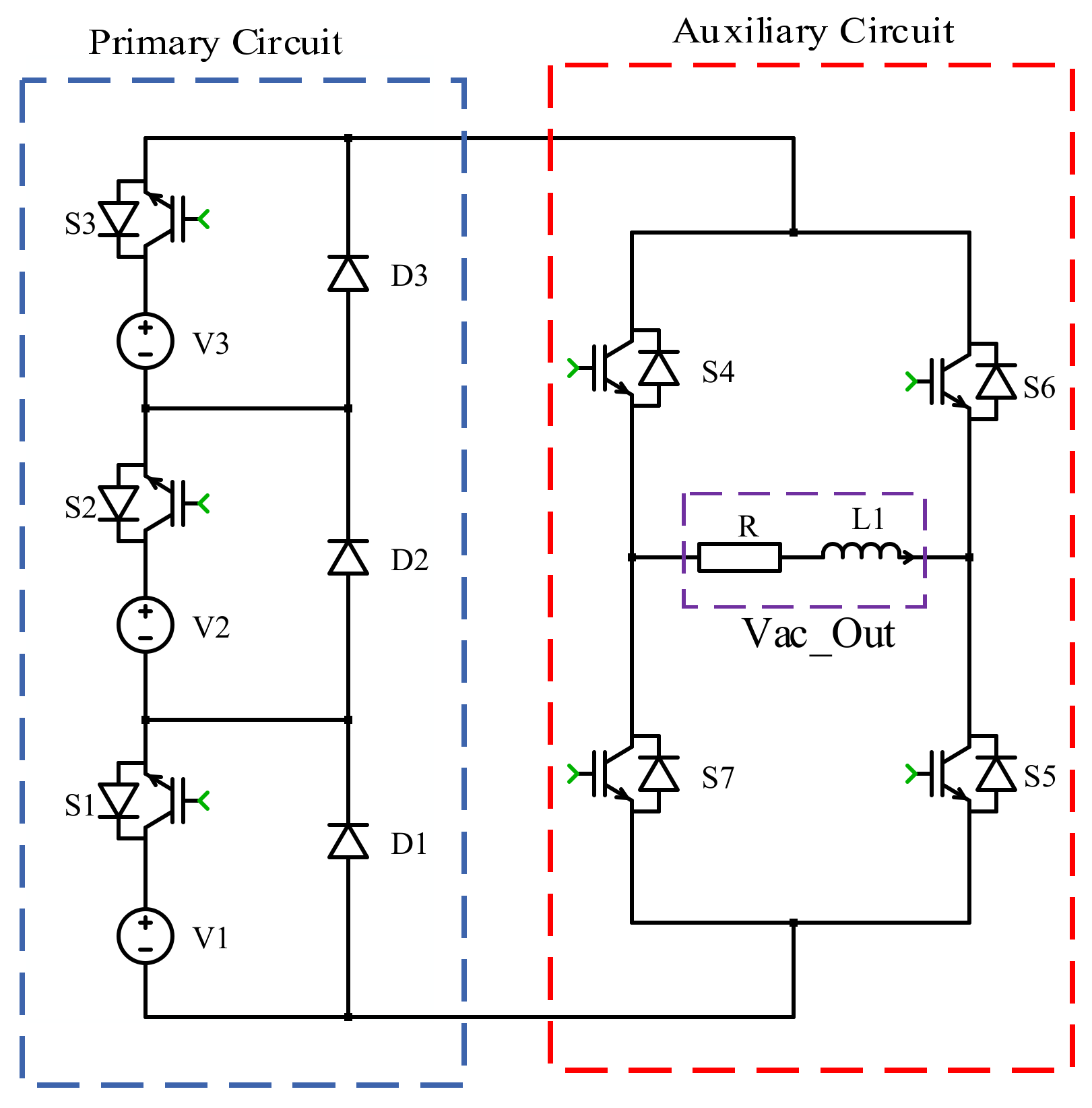
2. Proposed Asymmetric Multilevel Inverter

The proposed 15-level MLI consists of seven controlled semiconductor switches (IGBTs), three diodes and three dc sources. These elements are organized in a methodical manner to achieve the desired output levels. Figure 1 shows the proposed 15-level asymmetric MLI topology. It consists of a dc supply coupled in conjunction with a main switch and a bypass diode. When the switch ‘S’ is switched on, the source voltage ‘V’ arrives at the load; when the switch ‘S’ is off, the source voltage is separated from the load; hence, Vdc-out = ‘0’. The suggested inverter operates in both symmetrical and asymmetrical modes, based on input Power source.
The circuit’s dc voltage sources determine the output voltage. The proposed converter performs as an asymmetric inverter with different categories of dc sources. Table 1 shows the dc sources that can be used in the proposed inverter.
A similar magnitude approach produces symmetric dc sources of the same magnitude and can produce seven voltage output levels. Due to the symmetric nature of dc sources, they are not ideal for PV applications, where PV sources have variable output due to environmental changes/partial shading conditions. The second approach identifies unequal magnitude sources and produces eleven levels of output, but it is not a completely asymmetric design since V2 and V3 appear symmetrical in nature. The third method of selecting dc sources is the binary method, in which the input dc sources vary from one another and is ideal for PV applications. Multilevel inverters operate well with minimal switching and conduction losses at higher voltage levels; hence, the binary method was chosen for this study. As a result, the following voltages have been selected for 15-level output.
V1 = Vdc, V2 = 2Vdc, V3 = 4Vdc
Multilevel inverters may function in an asymmetrical manner using this approach, which is suited for fluctuating solar irradiation. For the numerous levels of output step voltages, as shown in Table 2, the switching sequence is described for each voltage level from +7Vdc to −7Vdc, along with the ‘0’ voltage level. During the auxiliary circuit’s +ve half cycle of output voltage, the switches S4 and S5 operate consistently, while the switches S6 and S7 operate during the -ve half cycle. The load gets short-circuited with switches S4 and S6 turned ON or with switches S5 and S7 turned ON, then the output level becomes to 0 V. By switching the main and auxiliary circuits according to Table 2, the inverter provides 15 output voltage levels.

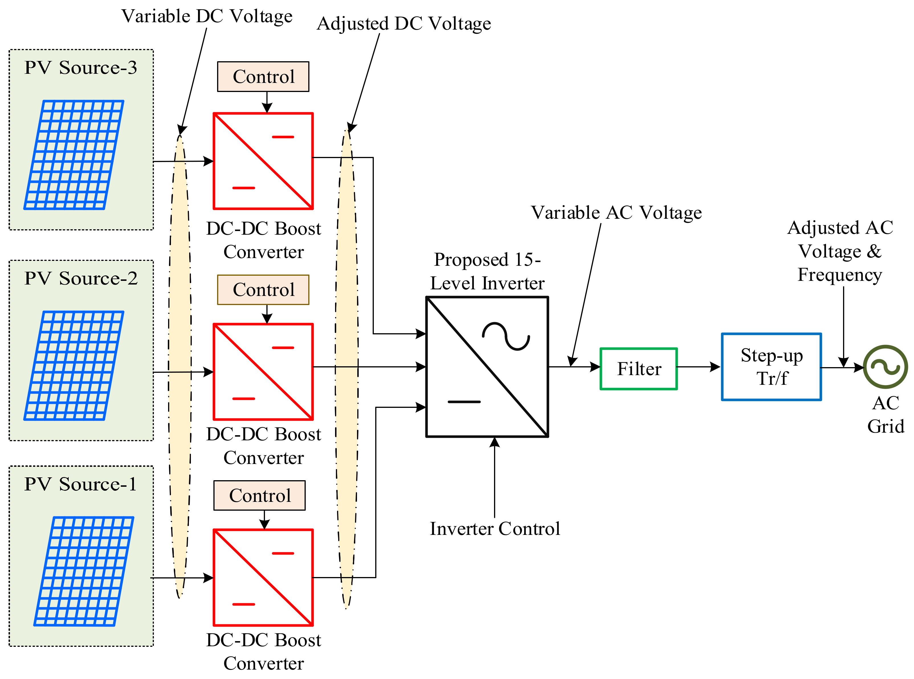
3. Grid Integration Methodology of Solar PV System

3.1. Two-Stage Grid-Connected SPV System

Figure 2 illustrates the suggested grid-connected solar photovoltaic system. In this system, the photovoltaic energy is integrated into the single-phase grid. The design model comprises a photovoltaic (PV) source, a boost converter, and an asymmetric inverter, among other components. PV cells are typically constructed of semiconductor materials and are capable of producing voltages ranging from 0.5 to 0.8 volts, which are quite low for real-time applications. To boost the voltage rating of a PV module, numerous PV cells (36 to 72) are coupled together in series to build a PV module. Connecting these PV modules in series and parallel to construct a larger array subsequently results in the formation of a photovoltaic (PV) panel. When PV modules are connected in series, the voltage rating of the PV module is increased; when PV modules are connected in parallel, the current rating of the PV module is increased.
The PV panel is responsible for supplying power to the boost converter. The boost converter, using the P & O MPPT algorithm, takes the highest power possible from the PV panel, which is then delivered to the inverter input using a dc-link capacitor. The dc-link capacitor helps to stabilize the dc-link voltage of a grid-connected system, which results in an increase in the voltage injected into the power grid. When it comes to the grid system, the inverter is a critical component, and it is linked to it at the point of common coupling (PCC) [20]. The grid is interfaced with the proposed 15-level inverter, which can supply maximum power throughout the day. This can be achieved by optimal converter, inverter and control circuit to enhance the overall system efficiency.

3.2. Implementation of Proposed Grid-Connected SPV System

Figure 3 depicts the proposed grid-connected photovoltaic system’s functioning block diagram. PV panels (or arrays), power converters, and the ac grid are the three essential components of the SPV system. Because PV arrays produce dc power, power electronic equipment must convert dc power into ac power. The grid-connected SPV system utilizes three PV sources for the three inputs of the proposed 15-level inverter. The dc power generated from three PV sources is fed to three separate boost converters controlled by the P & O MPPT algorithm to meet the input voltage requirements of the 15-level inverter. The inverter converts direct solar power into ac power and is crucial to operating an SPV system, although it is housed in sophisticated circuitry. The essential inverter features are the ability to work across a wide range of currents and voltages, output frequency, voltage regulation, and supply ac power with excellent power quality. The key innovation is the grid integration of a reduced switch 15-level inverter with solar photovoltaic systems. The inverter is controlled by the SHEPWM using a hybrid PSO-GA optimization algorithm, considering the grid voltage and grid currents are the reference parameters. In several locations worldwide, standalone power generating systems have been built without any grid connection. The grid-connected system is thus a practical compromise for high power requirements and the erratic quality of renewable energy [21].
The passive LCL filter then incorporates the suggested topology with the grid-connected system to further minimize the THD and improve waveform quality as per the grid requirements. The process of the proposed method is tested, and the selective test findings are presented in this chapter under standard test conditions.

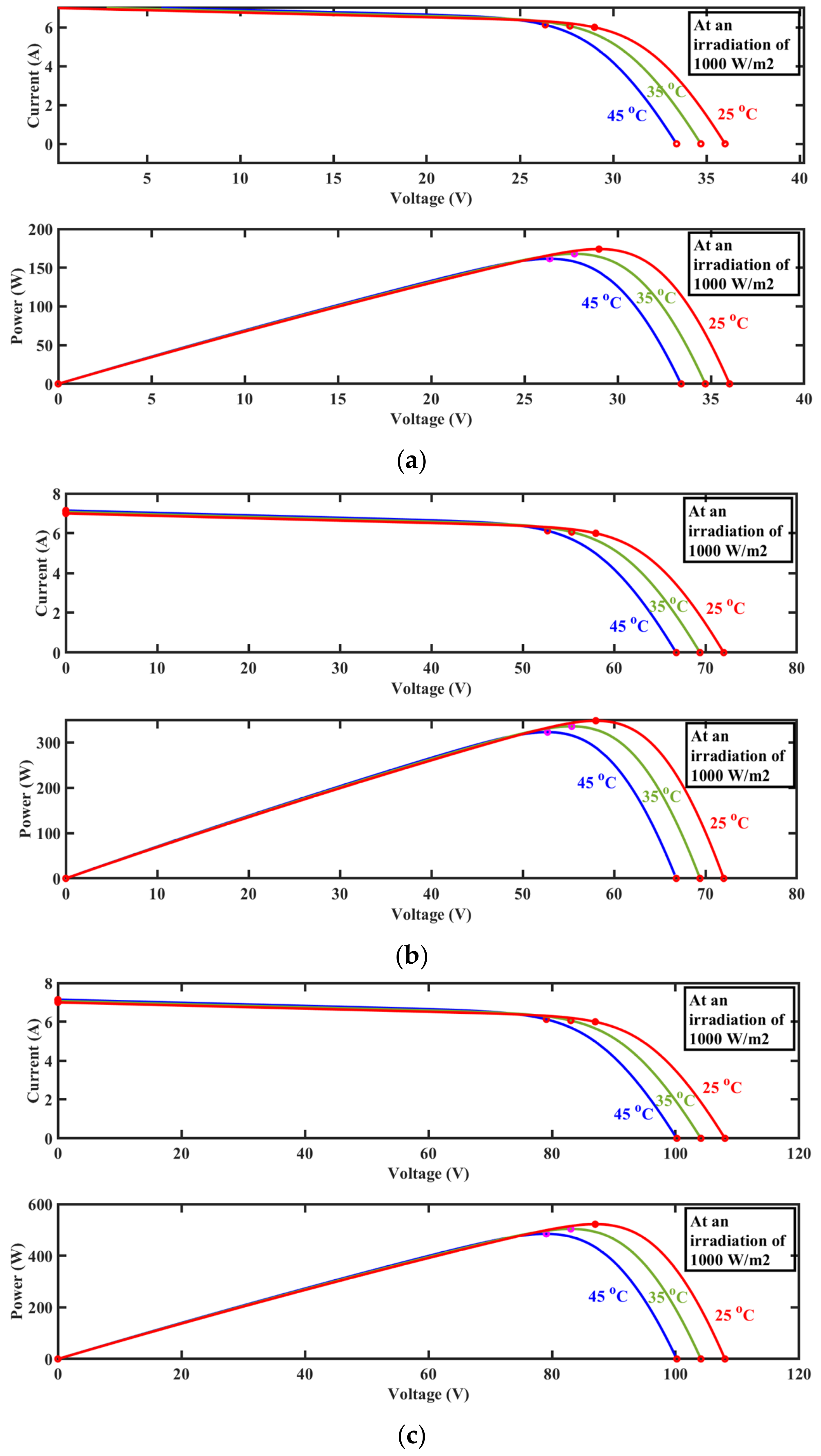
3.2.1. Modelling of SPV Sources

A PV module is a power generation unit of the SPV system. The amount of power that may be generated by photovoltaic modules has nonlinear features for both their I-V and P-V curves and is mostly dependent on the temperature and the level of irradiation. As a result, it is necessary to build a PV module in order to investigate its specific design, function, and the factors that contribute to the decrease in PV production. There are two major PV system design categories: single diode type and two diode type. Single diode type design is quite simple, but it does not consider the recombination of losses (constant ideality factor ‘1’) in the depletion layer. The two-diode type is efficient and frequently used to match an actual curve, with the second diode’s denominator of the exponential term’s argument comprising an ideality factor of ‘2’. Although one diode modelling is highly prevalent for PV modelling, it has the following downsides.
  • Temperature variations have a significant impact on photovoltaic performance. It prevents diffusion loss in the depletion region of PV cells.
  • The precision of the measurement was determined at low irradiance, in fact, at an open circuit. (Voc)
The two-diode model improves PV system accuracy, curve fitting, and eliminates one-diode model annoyance. Figure 4 shows the two-diode model’s equivalent circuit. It has an IPV and two diodes. In actuality, there are two extra series (Rser) and parallel resistances (Rsh). Solar cells aren’t ideal conductors; hence, they have series resistance. Any change in Rser affects PV cell output.
The design equations of PV cell are represented as follows;
I = I P h μ 1 μ 2   V S + 1 R s e r / R s h
where,
μ 1 = I d 1 e V s + 1 R s e r ε 1 V t 1
μ 2 = I d 2 e V s + 1 R s e r ε 2 V t 1
Here,
μ 1 = Current through diode D1, μ 2 = Current through diode D2, I d 1 = Saturation current of diode D1, I d 2 = Saturation current of diode D2, ε 1 = Emission coefficient of diode D1, ε 2 = Emission coefficient of diode D2, V s = PV cell voltage, V t = Terminal voltage of PV cell, I p h = Current produced in a photovoltaic cell.
Therefore, the current produced by the PV cell is represented in Equation (4).
I p h = I σ I s o / I σ 0
where,
I s o = Solar current, I σ   &   I σ 0 = Irradiance currents.
A solar panel is made up of 24 photovoltaic (PV) cells. Each photovoltaic cell has an open-circuit voltage of 0.5 V. At 1000 W/m2 and 25 °C, these solar PV cells are connected in series to generate 12 V. The choice PV sources for the proposed grid-connected system are PV1 = 48 V, PV2 = 96 V, and PV3 = 192 V to get a peak value of 336 V. Therefore, four 12 V modules are connected in series to generate a voltage of 48 V at the solar PV system’s output. Similarly, the 96 V output can be obtained by series connection eight 12 V modules, and series connection sixteen 12 V modules get 192 V output. The characteristics I-V and P-V of the PV1, PV2 and PV3 are presented in Figure 5 at a constant temperature of 25 °C for variable irradiance. The characteristics I-V and P-V of photovoltaic cell is illustrated in Figure 6 at constant (1000 W/m2) irradiance with varying temperature.
The three input sources required for the 15-level inverter are illustrated in Figure 7. These sources are dissimilar and asymmetric in nature with PV1 = 48 V, PV2 = 96 V, and PV3 = 192 V.
The total value of the dc-link voltages combing the three PV sources is illustrated in Figure 8. The simulated results give a peak value of 336 V.

3.2.2. Boost Converter Design for PV System

The dc-dc conversion is critical in photovoltaic systems since the voltage generated by the PV panels does not meet the load requirements. It is necessary to employ a boost converter in order to increase the voltage of the PV system. The boost converter gives maximum power to the proposed 15-level inverter throughout this operation. The typical design model of the boost converter (dc-dc) is illustrated in Figure 9. It includes the diode, IGBT switch, inductor, and capacitor. The purpose of the capacitor is to remove voltage disturbances in the output.
The inductor and capacitor are two critical components of a dc-dc converter that must be modelled to obtain the required output voltage. The inductor and capacitor are designed using fundamental mathematics.
L = V i n V o u t V i n Δ I L f s V o u t
C = I o u t δ f s Δ V C
where,
Δ I L = Inductor ripple current
Δ V C = Capacitor ripple voltage
δ = Duty cycle = V 0 V s V 0
f s = Switching frequency.
The values of inductor ripple current and capacitor ripple voltages are calculated using Equations (7) and (8), respectively.
Δ I L = 2 %   t o   4 % I o u t m a x V o u t V i n
Δ V C = 2 %   t o   4 % V o u t m a x I o u t I i n
where, V o u t is the maximum output voltage, V i n is the input voltage, I i n is the input current, I o u t m a x is the maximum output current.
There are three separate boost converters used for the three independent PV sources to boost the PV voltage as per the requirement of inverter input. These boost converters are employed with individual P & O MPPT controllers for the control of the duty cycle.

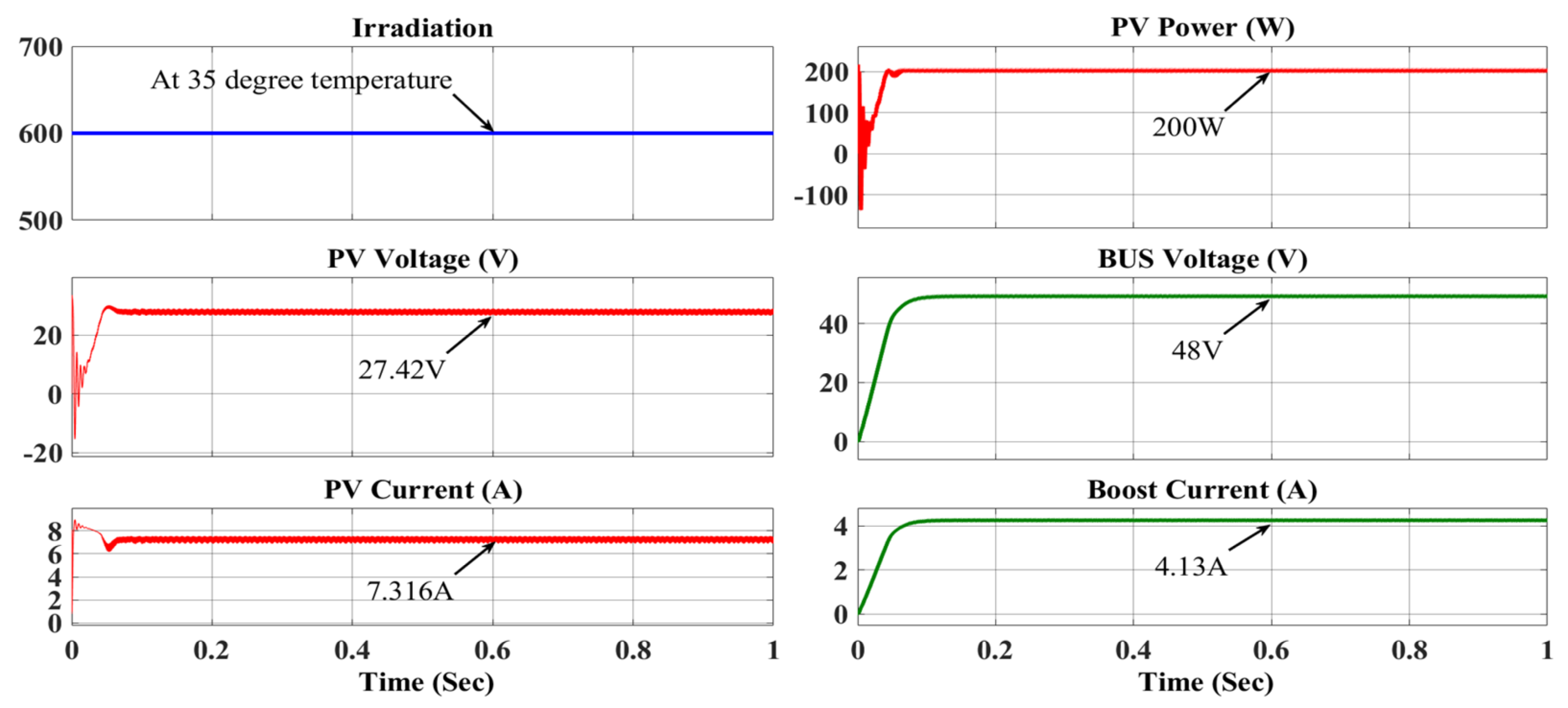
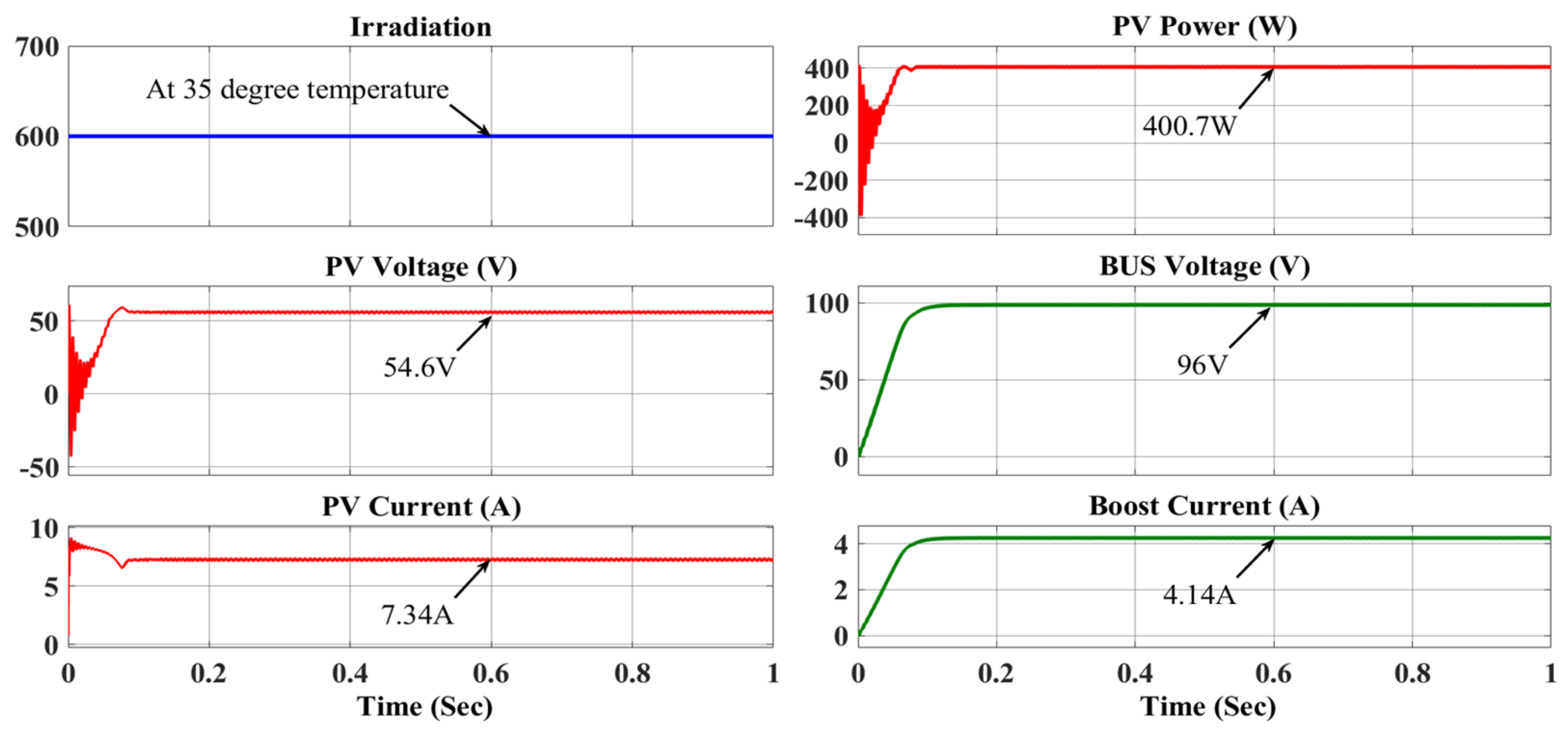
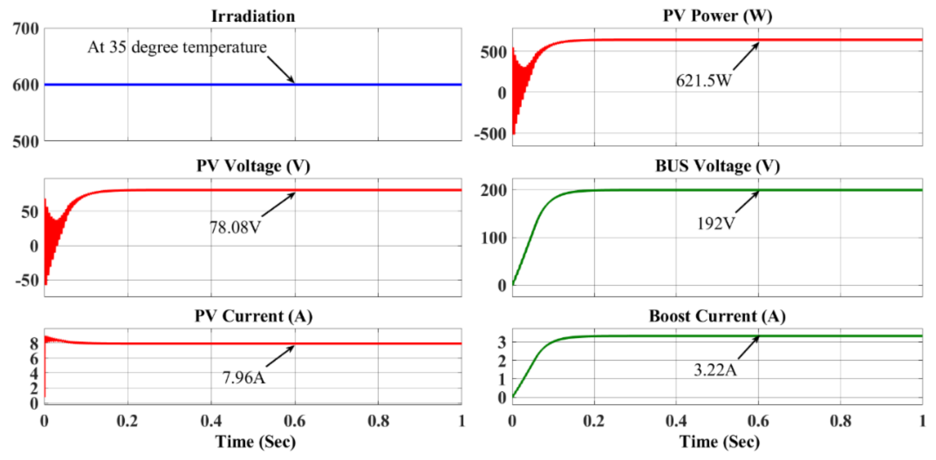
3.2.3. Simulation of PV Sources at an Irradiance of 600 W/m2 at a Temperature of 35 °C

In this case, the PV sources operated at practical test conditions with the irradiance of 600 W/m2 and temperature of 35 °C.
At this test condition, PV1 produces a power of 200 W with a voltage of 27.42 V and a current of 7.316 A. This voltage level is not sufficient for input-1 of the proposed inverter. PV1 voltage is increased from 27.42 V to 48 V with the help of a boost converter, and the corresponding output current is 4.13 A, as shown in Figure 10.
PV2 produces a power of 400.7 W with a voltage of 54.6 V at 7.34 A of current. But the inverter input ‘2’ is required 96 V. Hence, the PV2 voltage increased to 96 V from 54.6 V using a boost converter, giving an output current of 4.14 A, as shown in Figure 11.
Similarly, PV3 produces a power of 621.5 W with a voltage of 78.08 V at 7.96 A of current. But the inverter input ‘3’ is required 192 V. Hence, the PV3 voltage increased to 192 V from 78.08 V using a boost converter, giving an output current of 3.22 A, as shown in Figure 12.
Although, for analyzing the performance of the proposed inverter on practical operating test conditions of the PV system, an irradiance of 600 W/m2 and a temperature of 35 °C is considered. The control of grid parameters under these test conditions is described in the following sections.

3.2.4. Design of LCL Filter

In most cases, the filter is connected to both the inverter and the grid. The filter performs three essential functions: it reduces high-frequency noise, shields the transient, and converts the voltage to a current source. The L-type, LC-type, and LCL-type filters are the three primary filters used in grid-connected networks. The LCL filter is used to link the inverter with the grid in this application. In addition, the inverter operation is based on triggering of power switches and since the switches need gating pulses. Due to switching of the devices, the output current may include large harmonic distortions that aim to degrade the power quality of the power system. To remove the switching harmonics in the output of the inverter, an LCL filter is designed in this study. The criteria for calculating the model parameters are listed below.
The inductor at the inverter side is modelled with the Equation (9).
L i   = V d c   l i n k 8   f s   Δ I L
where,
Δ I L = inductor ripple current
f s = Switching frequency = 1000 Hz
V d c   l i n k = DC link voltage = 336 V.
Also, the inductor ripple current is evaluated using Equation (10)
Δ I L = 0.1   2   P V p h   g r i d
where,
P = Active power of the grid = 1250 W
V p h   g r i d = Phase voltage of the grid = 240 V.
The grid side inductor can be calculated using Equation (11)
L g   = 0.6   L i
The capacitance value is determined, considering 5% of the base capacitance using the Equation (12).
  C f = 0.05   C b
where,
C b   =   P ω g r i d     V g r i d 2
ω g r i d = Angular frequency = 2 π f = 314.2 rad/s.
V   g r i d = Phase voltage of the grid = 240 V

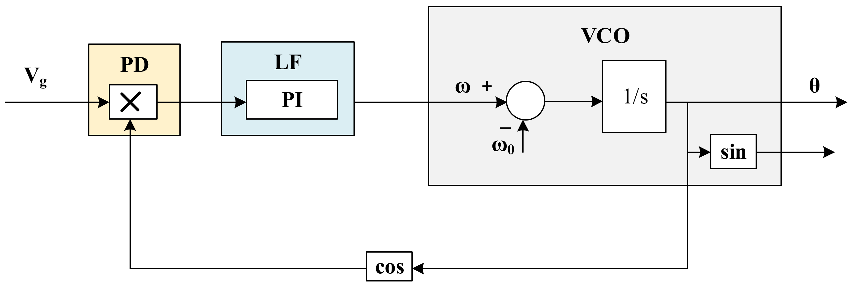
4. Control Methodology of Proposed Grid-Connected PV System

Asymmetric PV sources feed the input dc supply of the proposed inverter. The current into the grid is injected by using an adaptive PI controller. For the power factor to be maintained at unity, the current injection must be sinusoidal and in phase with the grid voltage [22]. Keeping the dc voltages generated by the PV array steady throughout the day is essential for producing sinusoidal current.
There are two different control strategies used for voltage control with PI controllers for injecting the current into the grid. One PI controller regulates the total dc voltage produced by the three PV sources and the other PI controller regulates the voltage of individual PV sources. Because asymmetrical PV inputs are supplied to the inverter through dc links, separate dc-dc boost converters with MPPT controllers are constructed for each PV source in the proposed configuration. Under various operating situations, these independent MPPT controllers keep the dc-link voltages in the 1:2:4 ratio. To produce the reference PV voltages such as V dc 1 * , V dc 2 * and V dc 3 * a P & O based MPPT algorithm is used.
Figure 13 illustrates the suggested grid-connected inverter’s control approach. It consists of a voltage controller, current controller, and a grid tracker. This controls the three separate dc sources and keeps their voltages in the proper ratio (1:2:4) to meet the grid codes.

4.1. Total dc Voltage Control

Figure 13 depicts the closed-loop voltage controller used to produce the required voltage in the dc link, which is comparable to the appropriate reference voltage for the specified irradiation level. The reference voltages ( V dc 1 * + V dc 2 * + V dc 3 * ) are compared with the actual voltages (Vdc1 + Vdc2 + Vdc3), to regulate the total dc voltage of the PV system and the corresponding error is processed through the PI controller. The PI controller consists of two gains like Kpv1, Kpi1, which are tuned by a hybrid PSO-GA optimization control to get the maximum value of reference current of the grid (Imax). A PLL generates the sinusoidal reference current ( I g * ) of the grid for the grid-connected system.
The PLL is usually employed for grid integration. The typical model of PLL is illustrated in Figure 14. The components of the PLL are a voltage-controlled oscillator, a low-pass filter controlled by a PI controller, and a phase detector. The phase detector block is responsible for detecting the phase difference between the input and feedback signals. The input of the phase detector block is provided by Equation (14).
V G t = 2   V grid   rms sin ω g t + φ
The output obtained from the phase detector block is represented in Equation (15).
V PD t = 2   V grid rms sin θ g cos θ ^
The Equation (15) further represented as,
V PD t = 2 2   V grid rms sin ω g ω ^ t + φ g φ ^ + sin ω g + ω ^ t + φ g + φ ^
There are two components in Equation (16) (high frequency and low frequency). When the phase detector’s output is transmitted through the PI-based LF block, the low-pass filter removes the high-frequency component, and the frequency component is retrieved at the LF block’s output.
V LF t = 2 2   V grid rms sin ω g ω ^ t + φ g φ ^
The PI controller will provide appropriate frequency. As ω g = ω g ^ and φ g = φ ^ , the output signal from the LF block indicated in Equation (17) tends to zero under the steady condition. By using the grid voltage as an input, the output phase signal is locked.

4.2. Grid Voltage and Grid Current Control

To produce the reference current needed by the grid, a PLL (phased lock loop) is used. The measured value (Igrid) is compared to the reference grid current Igrid*, and the error acquired is sent into the PI current controller. The grid current is maximized by changing the gains (Kp, Ki) of the PI controller. The current controller provides a reference signal Vk* during stable operating conditions, and the reference inverter voltage is obtained by subtracting the grid voltage signal from the reference inverter voltage. As a result, the inverter reference voltage changes in line with the grid voltage. When the grid voltage drops, the difference Vgrid − Vk* drops as well, and the reference voltage of the inverter drops as well with the grid tracker. The grid tracker’s output can be scaled to create a part of the inverter’s reference voltage.

4.3. Individual dc Voltage Control

For a 15-level asymmetric inverter, three unequal dc sources Vdc1, Vdc2, Vdc3, are used under various atmospheric conditions. In addition to the total dc voltage control, there exist two other voltage controllers, which are required to maintain the Vdc2, Vdc3 voltages at their reference voltages V dc 2 * and V dc 3 * . Grid frequency is generated by adding the sine component of the grid frequency (obtained via PLL) to both the total voltage controller and individual voltage controller outputs to form the reference signal for the inverter, which is then used to generate the PWM signals.

4.4. SHEPWM Control for Grid-Connected PV System

The selective harmonic elimination technique is used to establish the switching pulses to the inverter and to provide a waveform that is free of harmonics. Lower order harmonics are reduced by using the SHEPWM method, resulting in a smaller filter size for the system [24]. This method uses quarter-wave symmetry to cut down on computations. Hence the switching angles are computed between 0° and 90° (0° ≤ α ≤ 90°). The even-order harmonics in the Fourier expansion are ‘0′ because of the odd symmetry of the quarter-wave.
According to the following formula, the Fourier series is generated from the output of the inverter,
V 0 = a 0 + n = 1 A n cos n ω t + n = 1 B n sin n ω t
The even harmonics become zero in the output of the inverter because the analysis is considered the quarter-wave symmetry. Therefore, the Equation (18) can be written as,
V 0 = n = 1 B n sin n ω t  
where,
B n = 1 π   0 2 π V P V sin n ω t d ω t
Generally, the output of the multilevel inverter is the stepped wave; hence the Equation (20) is represented as,
B n = 2 π   0 π V P V sin n ω t d ω t
On integrating the Equation (21), the resultant B n can be written as
B n = 4 V P V k π   i z cos ( k α i )
Here, k represents the harmonic order, z represents the number of switching angles for the quarter-wave, α i Represents the ith switching angle, and VPV represents the voltage from the PV array. The number of triggering angles for an N-level output is represented in Equation (23).
Z = N 1 2  
where N represents output voltage levels of the inverter, therefore, from Equation (23), the switching angles needed to produce the 15 voltage levels is ‘7’. Hence, there are six nonlinear equations (excluding fundamental) to be solved for obtaining the seven switching angles of the 15-level inverter. These must fulfil the below constrain for the quarter-wave approximation.
α 1 < α 2 < α 3 < α 4 < α 5 < α 6 < α 7 < π 2
The fundamental voltage component always is set to modulation index ( M i ) , defined in Equation (25)
M i = V V P V
where V is the magnitude of the fundamental component, VPV represents the DC voltages fed from the SPV system. Therefore, the nonlinear equations generated from Equation (22) is solved using Particle Swarm Optimization (PSO), Harris Hawk Optimization (HHO) and a hybrid PSOGA algorithm, and the corresponding switching angles are stored in memory lookup tables for several modulation indexes. These switching angles are retrieved from the lookup tables for a given modulation index set by the dc-link voltage. Further, these switching angles trigger the seven switches in the proposed inverter to produce the corresponding voltage and currents.

5. Results and Discussion

5.1. Implementation of PSO-PI Controller for GCSPV System

The PSO variables necessary to configure the PI controllers of the total dc voltage control block and the current control block are shown in Table 3. The integral time absolute error is selected as the fitness function, and the PSO algorithm gives the gains of the two PI controllers while minimizing the fitness function. After 114 iterations, the best gain parameters for voltage gains of PI (KVp, KVi) and current gains of PI (KCp, KCi) controllers are achieved. The PSO tuned PI gains of the voltage and current controllers are given as KVp = 0.51, KVi = 0.209, KCp = 0.87, Kci = 0.341, respectively. A peak voltage of 336.8V and a peak current of 6.89A are shown in Figure 15, which is in phase with the grid voltage when utilizing PSO-PI control. Figure 16 shows the PSO-PI controller’s FFT analysis of the grid current waveform, which represents the overall harmonic distortion (3.96%).

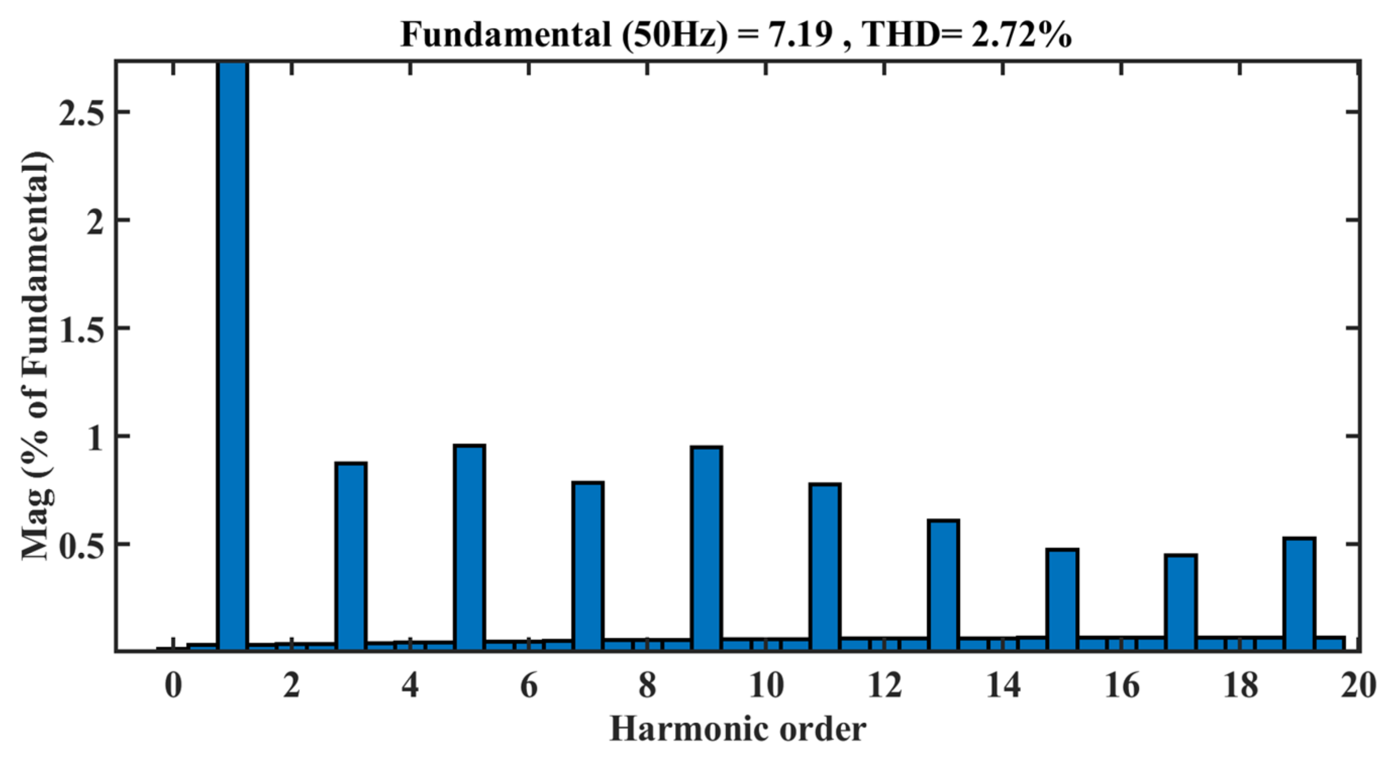
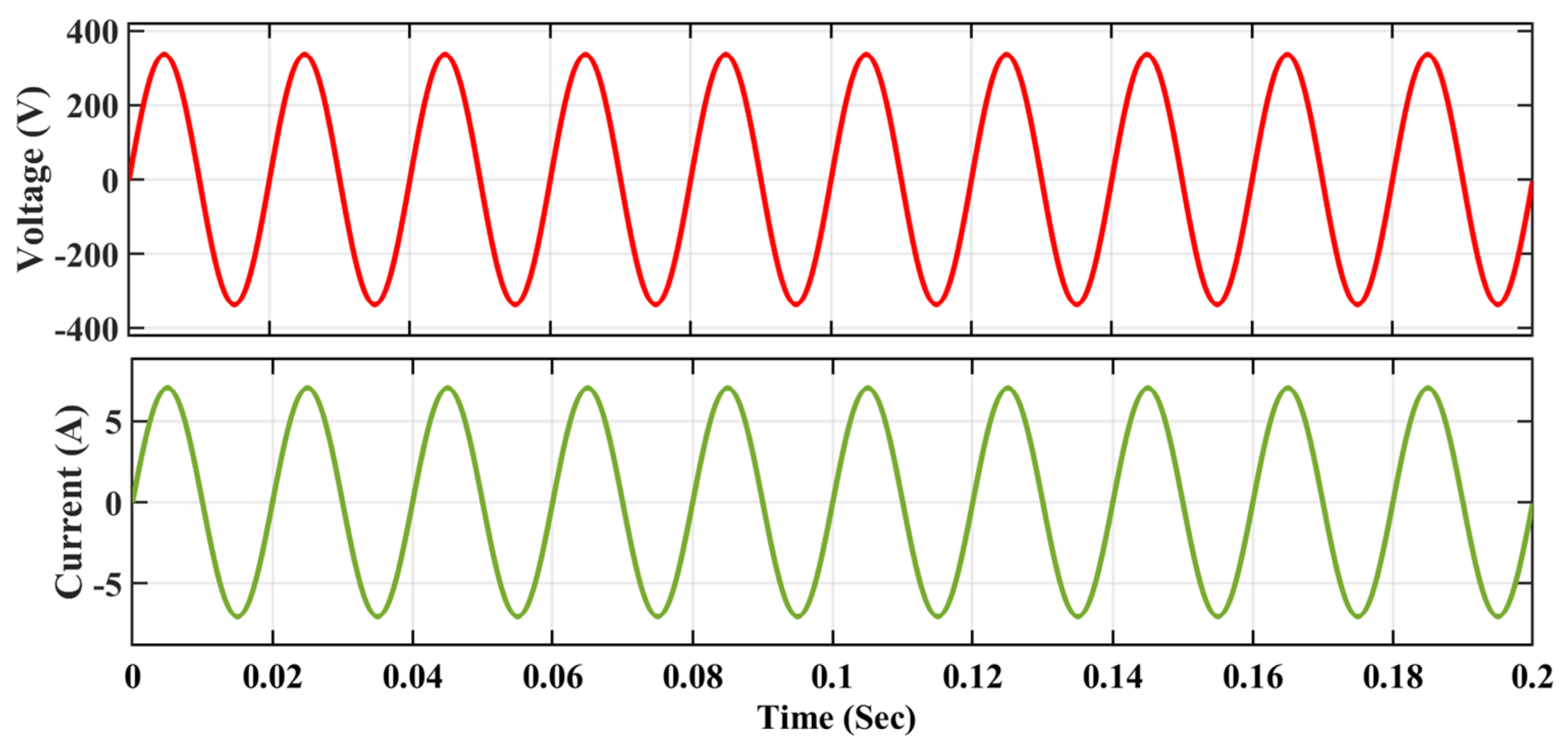
5.2. Implementation of HHO-PI Controller for GCSPV System

For the proposed control system’s total voltage controller block and current controller block, the HHO technique allows use of the integral time absolute error as the fitness function to determine the parameters of the PI controller, which is implemented as a PI controller. Equations (26) and (27) represents integral time absolute errors used as the fitness functions of HHO for tuning the gain values of total voltage control and current control blocks, respectively. The parameters and specifications involved in tuning the PI controller using the HHO algorithm are represented in Table 4.
I T A E = t   e t   d t = 0 t V D C r e f V D C a c t t t   . d t
I T A E = t *   e t   d t = 0 t I G R I D r e f I G R I D a c t t * t   . d t      
HHO uses 75 iterations to get the most acceptable voltage and current control gains of the PI controller. The optimum values of gain parameters are KVp = 0.81, KVi = 0.11, KCp = 0.91, Kci = 0.089 using HHO-PI controller for GCSPV system.
Figure 17 shows the grid voltage waveform and grid current waveform with a peak voltage of 336.7 V and peak current of 6.91 A, using HHO-PI control. The FFT analysis of grid current waveform, representing the total harmonic distortion (2.72%), is shown in Figure 18 using the HHO-PI controller.

5.3. Implementation of a Hybrid PSOGA-PI Controller for GCSPV System
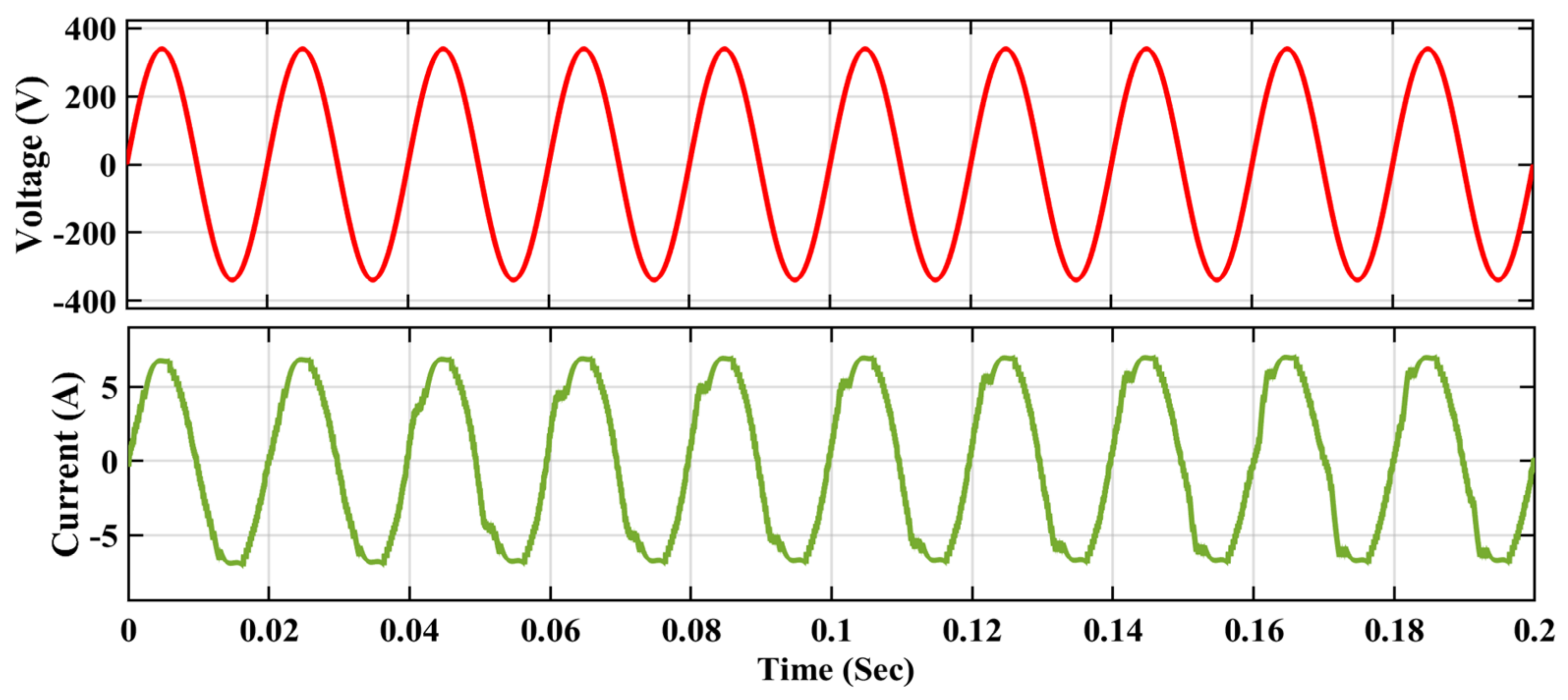
To overcome the problems of local minima and to improve the search accuracy hybrid PSOGA is implemented. The hybrid algorithm consists of the following stages.
Stage A: PSO parameters initialization.
Stage B: GA parameters initialization.
Stage C: At each case determine the GA optimal solution by arranging the PSO parameters.
Stage D: Execute the GA crossovers and mutation at GA optimal solution.
Stage E: Search for the best solution for both GA and PSO until the termination criteria.
Stage F: If the termination criteria not reached go to Stage C.
Stage G: If the generations are segregated according to the iterative items N, then the selection of P individuals should be based on their objective from the various sub-systems. When utilizing this strategy, the vector is improved by particle swarm optimization (PSO), and the decision vectors are updated through the application of genetic operators using the genetic algorithm (GA). With the introduction of genetic operators, such as crossover and mutation, into the PSO algorithm, it has been possible to further improve the balance between exploration and exploitation capability. In this case, the integral time absolute error is selected as the fitness function. In order to compute the gains of the two PI controllers while keeping the fitness function as small as possible, the PSO algorithm is utilized. The fitness function for the voltage controller of PI is represented by Equation (26) and the fitness function for the current controller of PI is represented by Equation (27), respectively. The optimum values of gain parameters are KVp = 0.96, KVi = 0.089, KCp = 0.94, Kci = 0.096 using PSOGA-PI controller for GCSPV system. The specifications and parameters used in hybrid PSOGA based PI tuning is presented in Table 5.
Figure 19 depicts the grid voltage and grid current waveforms, with a peak voltage of 336.7 V and a peak current of 6.96 A, respectively, when the PSOGA-PI control is used to regulate the grid voltage and grid current. Figure 20 depicts the results of an FFT analysis of the grid current waveform, which represents the overall harmonic distortion (1.26%) and was performed using the PSOGA-PI controller.
During the grid’s steady-state operation, the inverter is responsible for supplying active electricity to the grid. The suggested inverter injects current into the grid at a rate that is in phase with the grid voltage in order to preserve unity power factor. When the grid is operating in steady state, the active and reactive power are measured, and the associated waveforms of the system are shown in Figure 21. According to the measurements, the active and reactive powers are 1171 W and 26.09 VAr, respectively.
Figure 22 depicts the leakage current measured in the grid, which is in the order of 1.25 × 10⁻¹⁵ A (very low). The leakage current in the grid is very low and insignificant. Thus, this research concludes that the grid’s performance is good with the suggested inverter and control method. The leakage current is affected by the driver circuit’s design, grid voltage, and frequency of pulse width modulation, grid impedance, and filter interference. A comparison of various gain parameters and corresponding THDs of different grid-connected controllers with the proposed controller is presented in Table 6.
The performance of grid-connected PV systems with different grid controllers is described in terms of efficiency, as shown in Table 7. The grid power in terms of RMS values is 1 2   V g I g . Where, V g is the peak value of grid voltage, and I g is the peak value of grid current. The dc power of the PV system can be obtained using Equation (28).
PDC = (Vpv1Ipv1) + (Vpv2Ipv2) + (Vpv3Ipv3)
PDC = (27.42 × 7.31) + (54.6 × 7.34) + (78.08 × 7.96) = 1222.72 W.
Table 7. Efficiency of the proposed GCSPV system with different controllers.
ControllerPower from PV System (W)Grid Voltage
V g   ( V )
Grid Current
I g   ( A )
Grid   Power   1 2   V g I g   ( W ) % Efficiency
PSO-PI PDC = 1222.72336.86.891160.2894.89%
HHO-PI 336.76.911163.3395.14%
PSOGA-PI336.76.961171.7295.82%
Also, the comparative analysis of different controllers with other topologies presented in the literature is presented in Table 8. This comparative analysis shows that the proposed PSOGA-based PI controller performs satisfactorily with a low THD of 1.26% at 95.82% efficiency.
Due to continuous variations in solar irradiation and temperature, the power out of the PV Panel is affected. However, the maximum power output can be obtained from the PV panel using the maximum power point tracking technique. The proposed system employs the P & O MPPT algorithm to track the maximum power point of the PV system under varying environmental conditions and is tabulated in Table 9. From Table 9, it is observed that as the irradiance is decreased and affecting the grid voltage to decrease. However, the proposed controller allows the grid voltage variations ±6% to the nominal RMS voltage of 240 V.

6. Conclusions

The application of the proposed 15-level asymmetric inverter on grid integration of an SPV system was explored in this chapter. On the Simulink platform, a 1.25 kW grid-connected SPV system is modelled and tested. The proposed grid-connected solar photovoltaic system is put through its tests using a variety of solar irradiance and temperature conditions. When designing the proposed system to inject sinusoidal current into the grid, two voltage controllers are taken into consideration. The total dc voltage of the proposed inverter is controlled by one controller, while the dc voltage of the corresponding dc sources provided by the PV array is controlled by the other. A PI controller is used to control the grid voltage and current under changing irradiance and variable temperature circumstances, which adjusts the needed gain to maintain constant grid voltage in all weather conditions. The THDs obtained from PSO-PI, HHO-PI, and PSOGA-PI controllers are 3.96%, 2.72% and 1.26%, respectively. These comparisons conclude that the hybrid PSOGA based PI controller gives a good response with less THD of 1.26% than other controllers. Also, the GCSPV system with the proposed inverter works flawlessly, with an efficiency of 95.82% using a hybrid PSOGA based PI controller. Further to extend the research work presented in this article, future work can be considered in the following possibilities:
  • The investigations can be extended to operate the inverter, considering an array of renewable energy resources such as fuel cells, PV cells, wind energy, etc.
  • By extending the concepts and procedures deduced in the thesis, the fault-tolerant capability of the MLI can be carried out.
  • The performance assessment can be carried out by injecting reactive power into the grid. This further improves the efficiency of the inverter, but investigations are required into the lifetime of the inverter since the inverter’s performance will degrade with the injection of reactive power.
  • The real-time analysis can be carried out to validate the analytical results of the proposed work.
  • The investigations can be extended to optimize dc-link voltage of designed multilevel inverter with input energy storage system under varying operating conditions.
  • The proposed multilevel inverter topology can be applied for various stand-alone medium and high-voltage applications, such as induction motor drive, FACTS devices, and HVDC applications.
  • The suggested method can be extended to the three-phase systems.

Author Contributions

Conceptualization, D.G.K.; Data curation, A.G. and S.S.K.; Formal analysis, S.M.; Funding acquisition, A.H.M. and A.A.A.; Investigation, A.G., N.K.S., M.B., H.K. and A.H.M.; Methodology, N.V.S. and S.M.; Software, N.V.S. and A.A.A.; Validation, N.K.S. and M.B.; Writing—original draft, S.S.K.; Writing—review & editing, H.K. All authors have read and agreed to the published version of the manuscript.

Funding

This research received no external funding.

Institutional Review Board Statement

Not applicable.

Informed Consent Statement

Not applicable.

Data Availability Statement

The data sources employed for analysis are presented in the text.

Conflicts of Interest

The authors declare no conflict of interest.

Abbreviations

SPVSolar photovoltaic system
GCSPVGrid connected photovoltaic system
P & OPerturb and observe
MPPTMaximum power point tracking
MLIMultilevel inverter
SHEPWMSelective harmonic elimination pulse width modulation
PDPWMPhase disposition pulse width modulation
SVPWMSpace vector pulse width modulation
MVMedium voltage
HVHigh voltage
THDTotal harmonic distortion
VdcDC input voltage
FSFCFundamental switching frequency control
α   Switching angle
V 1 max Peak fundamental voltage
V 1 Actual fundamental voltage
k Degree of freedom
NNo of output voltage levels
OFObjective function
GAGenetic algorithm
PSOParticle swarm optimization
HHOHarris hawk Optimization
PSOGAParticle Swarm Optimization with Genetic Algorithm
VgridGrid voltage
VPVPV cell voltage
IPVPV cell current
PPVPV cell power
VBoostOutput voltage of dc-dc boost converter
IBoostOutput current of dc-dc boost converter
KVpProportional gain value of voltage controller
KViIntegral gain value of voltage controller
KCpProportional gain value of current controller
KCiIntegral gain value of current controller
PIProportional plus integral

References

  1. Arun, N.; Noel, M. Crisscross switched multilevel inverter using cascaded semi-half-bridge cells. IET Power Electron. 2018, 11, 23–32. [Google Scholar] [CrossRef] [Green Version]
  2. Alishah, R.; Hosseini, S.; Babaei, E.; Sabahi, M. A new general multilevel converter topology based on cascaded connection of sub multilevel units with reduced switching components, DC sources, and blocked voltage by switches. IEEE Trans. Ind. Electron. 2016, 63, 7157–7164. [Google Scholar] [CrossRef]
  3. Samadaei, E.; Sheikholeslami, A.; Gholamian, S.; Adabi, J. A square T-type (ST-type) module for asymmetrical multilevel inverters. IEEE Trans. Power Electron. 2018, 33, 987–996. [Google Scholar] [CrossRef]
  4. Saeedian, M.; Adabi, J.; Hosseini, S. Cascaded multilevel inverter based on symmetric–asymmetric DC sources with reduced number of components. IET Power Electron. 2017, 10, 1468–1478. [Google Scholar] [CrossRef]
  5. Alishah, R.; Hosseini, S.; Babaei, E.; Sabahi, M. Optimal Design of new Cascaded Switch-Ladder Multilevel Inverter Structure. IEEE Trans. Ind. Electron. 2017, 64, 2072–2080. [Google Scholar] [CrossRef]
  6. Agrawal, R.; Jain, S. Multilevel inverter for interfacing renewable energy sources with low/medium- and high-voltage grids. IET Renew. Power Gener. 2017, 11, 1822–1831. [Google Scholar] [CrossRef]
  7. Lee, S. Single-stage switched-capacitor module (S3CM) topology for cascaded multilevel inverter. IEEE Trans. Power Electron. 2018, 33, 8204–8207. [Google Scholar] [CrossRef] [Green Version]
  8. Gautam, S.; Kumar, L.; Gupta, S. Single-phase multilevel inverter topologies with self-voltage balancing capabilities. IET Power Electron. 2018, 11, 844–855. [Google Scholar] [CrossRef]
  9. Tariq, M.; Meraj, M.; Azeem, A.; Maswood, A.; Iqbal, A.; Chokkalingam, B. Evaluation of level-shifted and phase-shifted PWM schemes for seven level single-phase packed U cell inverter. CPSS Trans. Power Electron. Appl. 2018, 3, 232–242. [Google Scholar] [CrossRef]
  10. Barzegarkhoo, R.; Kojabadi, H.; Zamiry, E.; Vosoughi, N.; Chang, L. Generalized structure for a single phase switched-capacitor multilevel inverter using a new multiple DC link producer with reduced number of switches. IEEE Trans. Power Electron. 2016, 31, 5604–5617. [Google Scholar] [CrossRef]
  11. Sharifzadeh, M.; Vahedi, H.; Al-Haddad, K. New constraint in SHE-PWM for single-phase inverter applications. IEEE Trans. Ind. Appl. 2018, 54, 4554–4562. [Google Scholar] [CrossRef]
  12. Lee, S. A single-phase single-source 7-level inverter with triple voltage boosting gain. IEEE Access 2018, 6, 30005–30011. [Google Scholar] [CrossRef]
  13. Valderrama, G.; Guzman, G.; Pool-Mazun, E.; Martinez-Rodriguez, P.; Lopez-Sanchez, M.; Zuniga, J.A. Single-phase asymmetrical T-type five-level Transformerless PV inverter. IEEE J. Emerg. Sel. Top. Power Electron. 2018, 6, 140–150. [Google Scholar] [CrossRef]
  14. Rai, N.; Chakravorty, S. Generalized formulations and solving techniques for selective harmonic elimination PWM strategy: A review. J. Inst. Eng. India Ser. B 2019, 100, 649–664. [Google Scholar] [CrossRef]
  15. Kumar, D.G.; Ganesh, A.; Naga Malleswara Rao, D.S. Design and Analysis of a Novel Cascaded 15-Level Asymmetric Inverter Using PSO and Whale Algorithms. In Proceedings of the 2021 International Conference on Sustainable Energy and Future Electric Transportation (SEFET), Hyderabad, India, 21–23 January 2021; pp. 1–6. [Google Scholar] [CrossRef]
  16. Fang, X.; Du, E.; Zheng, K.; Yang, J.; Chen, Q. Locational pricing of uncertainty based on robust optimization. CSEE J. Power Energy Syst. 2021, 7, 1345–1356. [Google Scholar]
  17. Xiao, D.; Qiao, W. Hybrid scenario generation method for stochastic virtual bidding in electricity market. CSEE J. Power Energy Syst. 2021, 7, 1312–1321. [Google Scholar]
  18. Kumar, D.G.; Ganesh, A.; Bhoopal, N. Power loss analysis in 15 level asymmetric reduced switch inverter using PLECS thermal models. J. Eng. Sci. Technol. Rev. 2021, 14, 10–17. [Google Scholar] [CrossRef]
  19. Heidari, A.A.; Mirjalili, S.; Faris, H.; Aljarah, I.; Mafarja, M.; Chen, H. Harris hawks optimization: Algorithm and applications. Futur. Gener. Comput. Syst. 2019, 97, 849–872. [Google Scholar] [CrossRef]
  20. Ahmed, M.; Sheir, A.; Orabi, M. Real-time solution and implementation of selective harmonic elimination of seven-level multilevel inverter. IEEE J. Emerg. Sel. Top. Power Electron. 2017, 5, 1700–1709. [Google Scholar] [CrossRef]
  21. Bihari, S.; Sadhu, P. Design analysis of high level inverter with EANFIS controller for grid connected PV system. Analog. Integr. Circuits Signal Process 2020, 103, 411–424. [Google Scholar] [CrossRef]
  22. Makhamreh, H.; Trabelsi, M.; Kukrer, O.; Abu-Rub, H. An effective sliding mode control design for a grid-connected PUC7 multilevel inverter. IEEE Trans. Ind. Electron. 2021, 67, 3717–3725. [Google Scholar] [CrossRef]
  23. Shunmugham Vanaja, D.; Stonier, A.A. Grid integration of modular multilevel inverter with improved performance parameters. Int. Trans. Electr. Energy Syst. 2021, 31, e12667. [Google Scholar] [CrossRef]
  24. Shunmugham Vanaja, D.; Stonier, A. A novel PV fed asymmetric multilevel inverter with reduced THD for a grid-connected system. Int. Trans. Electr. Energy Syst. 2020, 30, e12267. [Google Scholar] [CrossRef]
  25. Satti, M.; Hasan, A. Direct model predictive control of novel H-bridge multilevel inverter based grid-connected photovoltaic system. IEEE Access 2019, 7, 62750–62758. [Google Scholar] [CrossRef]
  26. Lakshmi, M.; Hemamalini, S. Decoupled control of grid connected photovoltaic system using fractional order controller. Ain Shams Eng. J. 2018, 9, 927–937. [Google Scholar] [CrossRef]
Figure 1. Proposed 15-level asymmetric multilevel inverter.
Energies 15 07665 g001
Figure 2. Proposed two-stage grid-connected SPV system.
Energies 15 07665 g002
Figure 3. Schematic diagram of proposed grid-connected SPV system.
Energies 15 07665 g003
Figure 4. A two-diode model of photovoltaic cell.
Energies 15 07665 g004
Figure 5. I-V & P-V curves at a constant temperature of 25 °C with variable irradiances of 1000 W/m2, 800 W/m2and 600 W/m2 (a) PV1, (b) PV2 and (c) PV3.
Energies 15 07665 g005
Figure 6. I-V & P-V curves at constant irradiation (1000 W/m2) with variable temperatures of 25 °C, 35 °C and 45 °C (a) PV1, (b) PV2 and (c) PV3.
Energies 15 07665 g006
Figure 7. Asymmetric PV sources for the input of proposed 15-level inverter.
Energies 15 07665 g007
Figure 8. Total dc-link voltage of the three PV sources.
Energies 15 07665 g008
Figure 9. PV connected dc-dc boost converter.
Energies 15 07665 g009
Figure 10. PV measurements, boost voltage, current, and PV output power at an irradiance of 600 W/m2 and temperature of 35 °C for PV1.
Energies 15 07665 g010
Figure 11. PV measurements, boost voltage, current, and PV output power at an irradiance of 600 W/m2 and temperature of 35 °C for PV2.
Energies 15 07665 g011
Figure 12. PV measurements, boost voltage, current, and PV output Power at an irradiance of 600 W/m2 and temperature of 35 °C for PV3.
Energies 15 07665 g012
Figure 13. Grid-connected controller for proposed 15-level inverter [23]. ‘*’ refrers to the reference/base values in the figure.
Energies 15 07665 g013
Figure 14. A typical model of single-phase PLL.
Energies 15 07665 g014
Figure 15. Grid voltage and grid current waveforms with PSO-PI controller.
Energies 15 07665 g015
Figure 16. THD analysis of grid current waveform with PSO-PI controller.
Energies 15 07665 g016
Figure 17. Grid voltage and grid current waveforms with HHO-PI controller.
Energies 15 07665 g017
Figure 18. THD analysis of grid current waveform with HHO-PI controller.
Energies 15 07665 g018
Figure 19. Grid voltage and grid current waveforms with PSOGA-PI controller.
Energies 15 07665 g019
Figure 20. THD analysis of grid current waveform with PSOGA-PI controller.
Energies 15 07665 g020
Figure 21. Active and reactive power delivered to the grid.
Energies 15 07665 g021
Figure 22. Leakage current in the grid-connected PV system.
Energies 15 07665 g022
Table 1. Choice of DC voltages for the proposed MLI topology.
ApproachDC VoltagesO/p StepsO/p LevelsMax. O/p Voltage
Identical VoltageV1 = V2 = V3 = Vdc473Vdc
Unequal MagnitudeV1 = Vdc, V2 = V3 = 2Vdc6115Vdc
Binary ApproachV1 = Vdc, V2 = 2Vdc, V3 = 4Vdc8157Vdc
Table 2. ON switches, power flow paths, and corresponding output levels of proposed 15-level inverter.
Switching OperationPower FlowOutput Voltage
S1, S2, S3, S4 & S5V1+ S1 V2   S2 V3 S3 S4 Load S5   V1+7Vdc
S2, S3, S4 & S5V2+ S2 V3 S3 S4 Load S5 D1 V2+6Vdc
S1, S3, S4 & S5V1+ S1 D2   V3 S3 S4 Load S5 V1+5Vdc
S3, S4 & S5V3+ S3 S4 Load S5 D1   D2 V3+4Vdc
S1, S2, S4 & S5V1+ S1 V2 S2   D3   S4 Load S5 V1+3Vdc
S2, S4 & S5V2+ S2 D3 S4   Load S5 D1   V2+2Vdc
S1, S4 & S5V1+ S1 D2 D3   S4   Load S5 V1+Vdc
S4 & S6 (or) S5 & S7S4   Load S6 S4 (or) S5   Load S7 S50
S1, S6 & S7V1+ S1 D2 D3   S6   Load S7 V1−Vdc
S2, S6 & S7V2+ S2 D3 S6   Load S7 D1   V2−2Vdc
S1, S2, S6 & S7V1+ S1 V2 S2   D3   S6 Load S7 V1−3Vdc
S3, S6 & S7V3+ S3 S6 Load S7 D1   D2 V3−4Vdc
S1, S3, S6 & S7V1+  S1 D2   V3 S3 S6 Load S7 V1−5Vdc
S2, S3, S6 & S7V2+  S2 V3 S3 S6 Load S7 D1 V2−6Vdc
S1, S2, S3, S6 & S7V1+  S1 V2   S2 V3 S3 S6 Load S7   V1−7Vdc
Table 3. Parameters & specifications of PSO.
ParametersValues
Size of population50
Cognitive factor C10.5
Social factor, C21.25
Inertia Weight, W1
Maximum velocity10
Number of iterations200
Table 4. Specifications and parameters of HHO.
ParametersValues
Number of Hawks’ N’30
Random generations r1, r2, r3, r4In the range of [0, 1]
Number of search agents7
Initial energy (E0)[–1, 1], [−1, 0] loosing energy,
[0, 1] raising energy
Convergence probability ‘r’0.5
Number of iterations200
Table 5. Specifications and parameters of hybrid PSOGA.
ParametersValues
Population size from50
Crossover fraction0.8 as default
Number of iterations200
Mutation rate0.006
Cognitive factor, C10.5
Social factor, C21.25
Inertia Weight, W1
Table 6. Comparison of gain parameters and THDs of proposed GCSPV system.
ControllerGain Parameters% THD
Voltage ControllerCurrent Controller
KVpKViKCpKCi
PSO-PI 0.510.2090.870.3413.96%
HHO-PI 0.810.110.910.0892.72%
PSOGA-PI0.960.0890.940.0961.26%
Table 8. Comparative analysis with other techniques proposed in the literature.
AuthorsControllerLevel of the Inverter% THD% Efficiency
Bihari and Sadhu et al. [21]EANFIS270.78%-
PI2718.19%-
PID2716.11%-
Makhamreh et al. [22]MPC73.45%-
Satti and Hasan et al. [25]DMPC72.7%95.3%
Lakshmi and Hemamalini et al. [26]PI33.32%-
FO-PI32.62%-
Dishore Shanmugam Vanaja et al. [24]HHO-PI311.49%94%
ProposedPSO-PI153.96%94.89%
HHO-PI152.72%95.14%
PSOGA-PI151.26%95.82%
Table 9. Impact of solar irradiance and temperature on grid connected PV systems.
PV Source & IrradianceTemperature in (deg.C)VPV (V)IPV (A)PPV (W)VBoost (V)IBoost (A)Grid Voltage (V)Grid Current (A)
MeanRMSMeanRMSMeanRMSMeanRMSMeanRMSRMSRMS
PV Source-1

600 W/m2
35 °C31.732.17.087.09223.8226.245.445.94.544.59237.85.74
PV Source-2

800 W/m2
30.0430.79.129.14275.9278.150.250.75.025.07
PV Source 3

1000 W/m2
28.728.911.111.231932153.854.25.385.43
PV Source 1

500 W/m2
25 °C3434.56.016.02203.420643.343.84.334.38241.25.61
PV Source 2

600 W/m2
33.834.26.946.95233.5236.146.446.94.614.69
PV Source 3

800 W/m2
32.132.39.159.20291.7294.251.752.25.175.22
Publisher’s Note: MDPI stays neutral with regard to jurisdictional claims in published maps and institutional affiliations.

