Article

Research and Development of Adjustable Discontinuous Pulse Width Modulation Method for Three-Phase Voltage Source Inverter

Electric Power Institute, Nizhny Novgorod State Technical University n.a. R.E. Alekseev, 603950 Nizhny Novgorod, Russia
*
Author to whom correspondence should be addressed.
Energies 2022, 15(20), 7463; https://doi.org/10.3390/en15207463
Submission received: 18 August 2022 / Revised: 30 September 2022 / Accepted: 6 October 2022 / Published: 11 October 2022
(This article belongs to the Special Issue Smart Solutions and Devices for the Power Industry)

Abstract

:
Continuous pulse width modulation (CPWM) and discontinuous pulse width modulation (DPWM) strategies are used to control voltage source inverter operation. CPWM strategies allow for the reduction of total harmonic distortion values, while DPWM strategies provide a more effective reduction in inverter switching losses. The paper is devoted to the problem of improving the three-phase voltage source inverter efficiency by a controlled transition from CPWM to DPWM. The article proposes an adjustable discontinuous pulse width modulation (ADPWM) method, which means a transition from space vector PWM (refers to CPWM strategies) to DPWM in all inverter phases when the switches’ temperatures exceed the allowable value in at least one of the inverter phases. The method flowchart is presented and an algorithm for modifying the envelope curve within one sector is given. In order to test the ADPWM method a Simulink-model of a three-phase voltage source inverter and its control system were developed. A study of the proposed ADPWM method’s efficiency in comparison with CPWM, PCDPWM and NCDPWM methods was carried out using a Simulink-model. It was established that the proposed ADPWM method provides dynamic losses reduction in the inverter switches by 2.86 times compared to CPWM and by 1.89 times compared to PCDPWM and NCDPWM methods. Power supply systems for medium and high-power AC motors provide a promising area for application of the proposed ADPWM method.

1. Introduction

Three-phase voltage source inverters are widely used in various industries; they are used as the main converting devices in electric drives, uninterruptible power supplies, and automation systems [1]. Reducing switching losses on the inverter switches (which can reach up to 50% of the total losses) and reducing harmonic distortion of the output voltage are important tasks for improving the efficiency of inverters. These tasks are solved by applying various pulse width modulation (PWM) strategies [2]. Modulation strategies can be classified into two categories including continuous pulse width modulation (CPWM) and discontinuous pulse width modulation (DPWM) [3].
Sinusoidal PWM (SPWM) and space vector PWM (SVPWM) are two typical CPWM strategies. SPWM is the classic PWM strategy [4]. The advantage of SPWM is the ease of implementation based on analog microcircuits. However, a serious disadvantage of SPWM is the incomplete DC voltage utilization factor. Currently, the preferred CPWM method is SVPWM. SVPWM is based on the method of introducing a triangular zero-sequence signal into phase voltages envelope curves [5,6]. An important advantage of SVPWM is the ability to fully utilize DC voltage. DPWM strategies are characterized by the use of zero-sequence signals of various forms to control the inverter switches [7]. DPWM strategies are aimed at reducing switching losses by reducing the number of transistor switches in the main cycle with utilization factor of DC voltage preserved [8]. Using DPWM is a relatively easy way to reduce the inverter switching loss [9]. Therefore, a large number of scientific articles have been devoted to improving the inverter efficiency applying DPWM strategies.
A DPWM method to reduce switching losses in a three-phase inverter is presented in [10]. A DPWM method to reduce switching losses for high power applications with low switching frequency is studied in [11]. A space vector-based general DPWM strategy for a low modulation region that ensures minimum switching instances by changing different templates is presented in [12].
According to the difference of the clamped ways, the DPWM method commonly used can be divided into the following six types, DPWM0, DPWM1, DPWM2, DPWM3, DPWMMAX and DPWMMIN [13]. Four conventional space vector-based DPWM strategies (DPWM0-DPWM3) for a three-level converter are presented in [14]. DPWM0-DPWM3 strategies to reduce switching losses depending on the power factor are studied in [15]. DPWM1-DPWM4 strategies for applications with large fsw to f1 ratios are considered in [16]. Reducing inverter switching losses by using DPWM with a constant clamping interval of 60 electrical degrees is studied in [17].
For the voltage vector, the DPWM pattern can be implemented with clamping to a positive bus bar of the DC link (PCDPWM) or to negative (NCDPWM). In [18], PCDPWM envelope curves were calculated through the injection of a zero-sequence signal in sinusoidal phase reference voltages. For NCDPWM, the algorithm is similar. In [19] it is shown that PCDPWM and NCDPWM can reduce switching losses by 33% compared to CPWM.
Thus, according to the scientific research results, DPWM compared to CPWM reduces switching losses in the inverter more effectively. At the same time, a common disadvantage of DPWM strategies is an increase in the amplitude of large neutral-point voltage ripple that influences the output voltages and currents [20]. It also increases the total harmonic distortion (THD) value [21].
PWM methods based on adjustable transition from CPWM to DPWM are being developed to overcome these weaknesses and provide a compromise between output voltage harmonic distortion and switching losses.
The combination of two PWM methods was investigated by analyzing the power losses and current THD in [22]. The effectiveness of the proposed DPWM method was demonstrated through simulations and experiments. A method to improve system efficiency by switching CPWM and DPWM modes was proposed in [23]. The proposed method is based on taking into account the modulation ratio. A DPWM strategy with the ability to control the period without switching is presented in [24]. Under the proposed strategy the period without switching can be adjusted within 0 to 120 electrical degrees’ range of the main period. In the methods presented, the transition from CPWM to DPWM is carried out disregarding the temperature of inverter switches. A combined use of a DPWM strategy to reduce switching losses taking into account the inverter switches temperature is proposed in [19]. However, the transition to the modified PWM method is carried out only in the phase of the inverter where the switches’ temperatures exceed the maximum allowable value. This can lead to unbalance in the three-phase voltage system. Another method of transition from CPWM to DPWM was proposed in [25]. This paper introduced a method which uses two categories of DPWM sequences. Using these two sets of sequences a generalized algorithm was proposed which gives optimal performance both in terms of line current distortion and inverter switching losses.
This article is devoted to the problem of increasing the three-phase voltage source inverter efficiency by reducing switching losses through adjustable transition from SVPWM to DPWM. The main contribution of this paper is the research and development of an adjustable discontinuous pulse width modulation (ADPWM) method. The method implies switching from SVPWM to DPWM in all inverter phases when the temperature of the switches exceeds the allowable value in at least one of the inverter phases.
The novelty presented in this article concerning the ADPWM method in comparison with relevant existing techniques lies in the stabilization of the inverter temperature by reducing dynamic losses. The authors expected that changing the reference voltage will make it possible to reduce the number of transistors switching, which leads to a decrease in dynamic losses. Thus, the thermal power released in the inverter decreases with its temperature. However, the THD of phase currents and voltage curves increases. In this case, applying the adjustable transition from CPWM to DPWM will smoothly reduce dynamic losses and smoothly increase THD. The article is organized as follows: a flowchart and a mathematical description of the proposed ADPWM method are presented in Section 2. Section 3 is devoted to the development of a Simulink-model designed to test the proposed method and other CPWM and DPWM strategies. Section 4 shows the proposed ADPWM method research results in comparison with CPWM, PCDPWM, and NCDPWM methods.

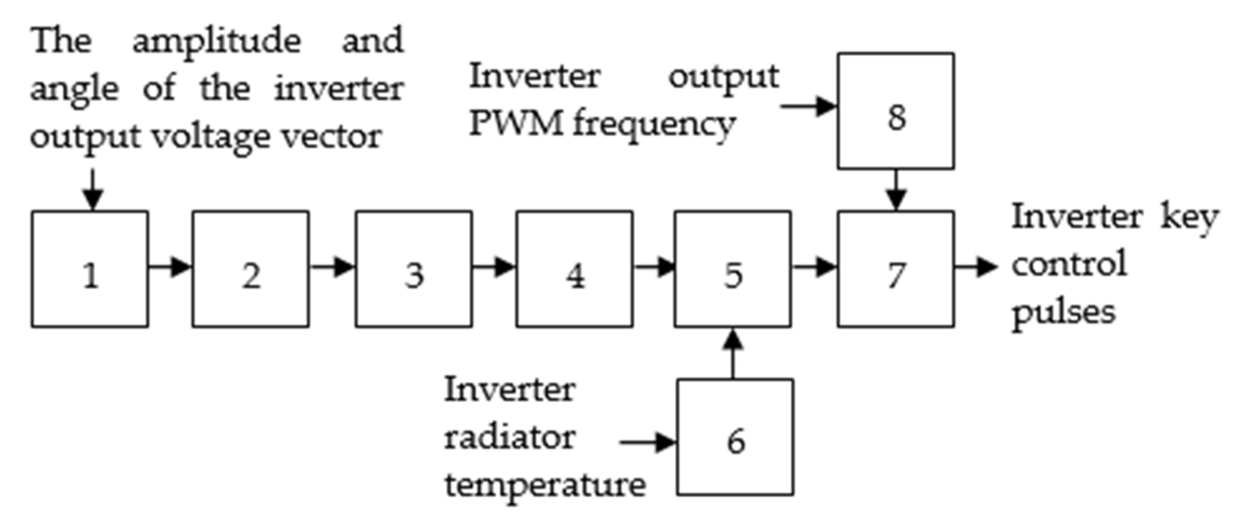
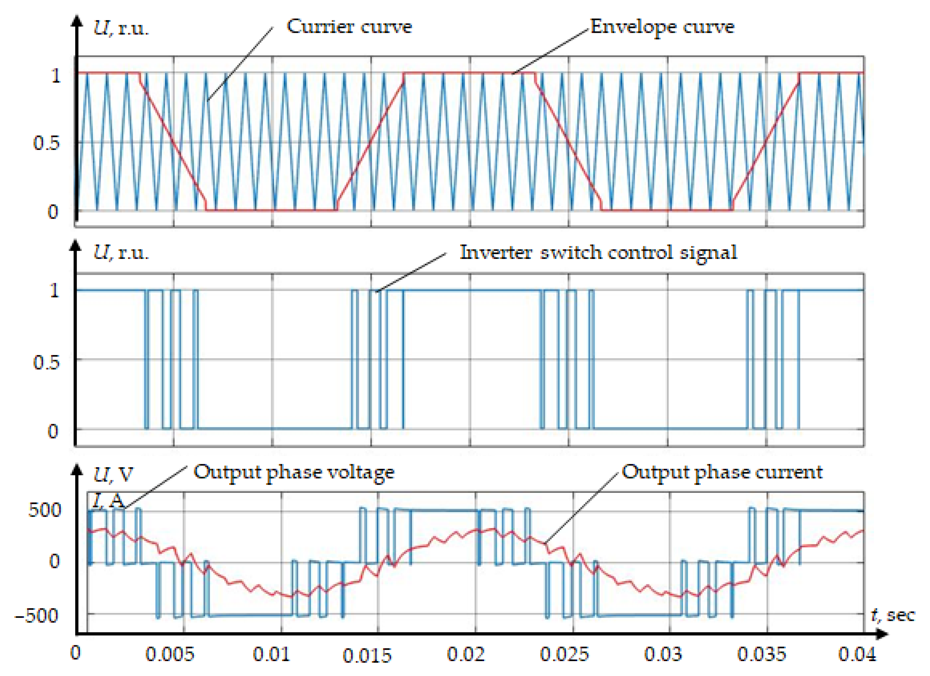
2. The Proposed Three-Phase Inverter Control Method

The developed ADPWM method is illustrated by the flowchart in Figure 1.
The input data are the following:
  • unit 1 input—amplitude and angle of inverter output voltage vector;
  • unit 6 input—inverter radiator temperature;
  • unit 8 input—PWM frequency of inverter output voltage.
Switch control pulse generation of the three-phase voltage source inverter is carried out as follows.
After receiving input data unit 1 calculates the sixty-degree sector number in which the inverter output voltage vector will be formed. Unit 2 calculates the output voltage vector angle within a sixty-degree sector. Based on these data, unit 3 calculates the base vector connection time and pause time according to the system of equations:
Tb1 = A · sin (60° − β);
Tb2 = A · sin (β);
T0 = 1 − Tb1Tb2,
where Tb1—is the connection time length of the first base vector (relative units); Tb2 is the connection time length of the second base vector (relative units); T0—is the connection time length of the zero-base vector (relative units); A—is the output voltage vector amplitude (relative units); β—is the angle inside the sixty-degree sector (degrees).
Next, based on the calculated values of the base vectors’ connection time and the pause time, unit 4 generates envelope curves of the inverter phase voltages in accordance with the classical SVPWM algorithm [26].
Based on the radiator temperature value of the three-phase voltage source inverter, unit 6 calculates envelope curve angles of connection of the output phase inverter voltage to a positive or negative value of the amplitude value of inverter output phase voltage. The duration of these segments is determined by the angle of connection. The angle of connection maximum value can be 120 electrical degrees. Angle of connection is:
  • equal to zero when the temperature of the inverter radiator is less than the threshold value;
  • directly proportional to the difference between the threshold and current values of inverter radiator temperature when the temperature of the inverter radiator is above the threshold value.
Angle of connection is calculated using the formula:
θ = 0 , T T M I N θ M A X T M A X T M I N T θ M A X ( θ M A X T M A X T M I N 1 ) , T T M I N
where θ—is the angle of connection (electrical degrees); T—is the current radiator temperature (degrees); θMAX—is the maximum angle of connection value (θMAX = 120); TMIN—is the minimum temperature at which the algorithm starts working; TMAX—is the maximum temperature at which θMAX is reached.
Based on angle of connection calculated values, unit 5 modifies the envelope curves of inverter output phase voltages. To do this, the range of clamping of phase voltages envelope curves within each sector is calculated. In this case, only two-phase curves are bound within one sector:
  • for sector 1—curves of phases A and C;
  • for sector 2—curves of C and B phases;
  • for sector 3—curves of phases B and A;
  • for sectors 4, 5 and 6—similar to sectors 1, 2 and 3.
The clamping ranges are calculated in accordance with the formulas:
C1 = sin (θ · π/360);
C2 = sin [(π/3) − (θ · π/360)].
The flowchart of modification algorithm of envelope curve inside sector 1 is shown in Figure 2.
Envelope curves modification algorithm is as follows. If the section of the envelope curve of inverter output phase voltage is within the binding range, the envelope curve value in this section is:
  • equal to the positive value of inverter output phase voltage amplitude during the formation of a positive half-wave of inverter output phase voltage;
  • equal to the negative value of inverter output phase voltage amplitude during the formation of a negative half-wave of inverter output phase voltage.
Unit 7 compares the modified envelope curves of inverter output phase voltages and PWM triangular reference voltage of a given frequency, which is generated by unit 8. The control pulses of three-phase voltage source inverter switches are generated at unit 7 output.
Changing the reference voltage makes possible to reduce the number of transistors switching, which leads to a decrease in dynamic losses. Thus, the thermal power released in the inverter decreases with its temperature.
Thus, the proposed ADPWM method makes it possible to reduce the number of inverter switches when inverter radiator temperature exceeds the limit value.

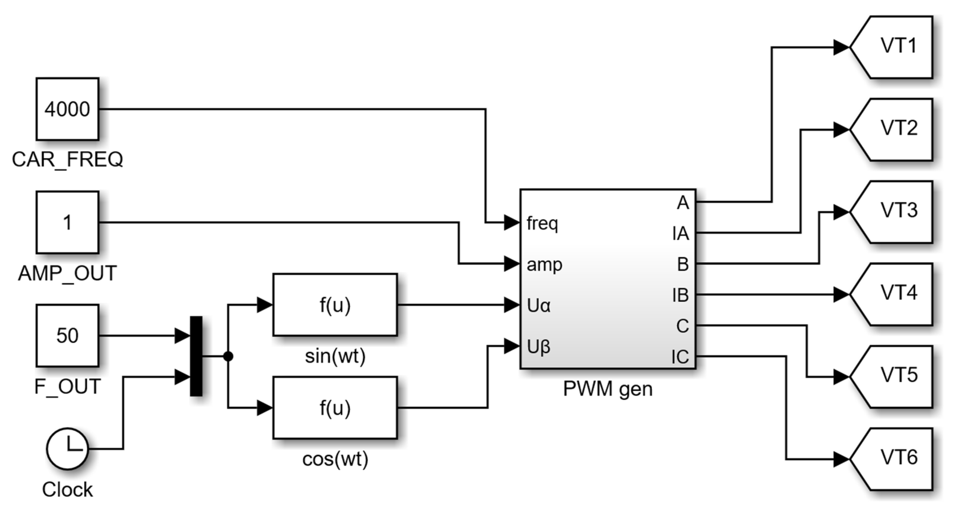
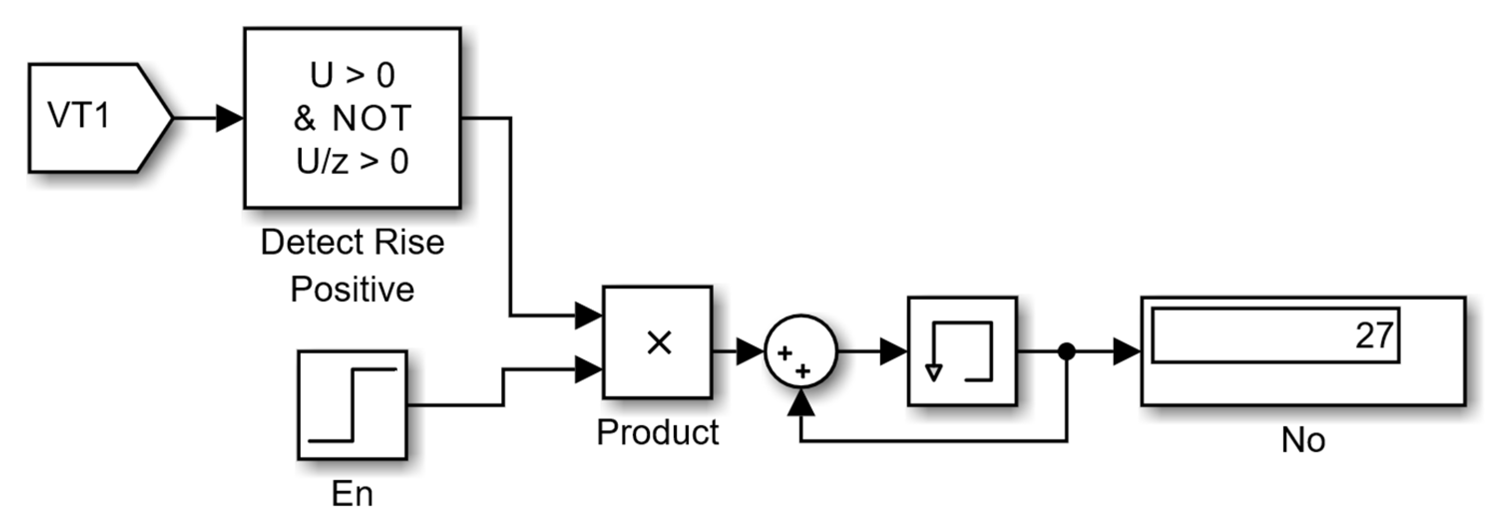
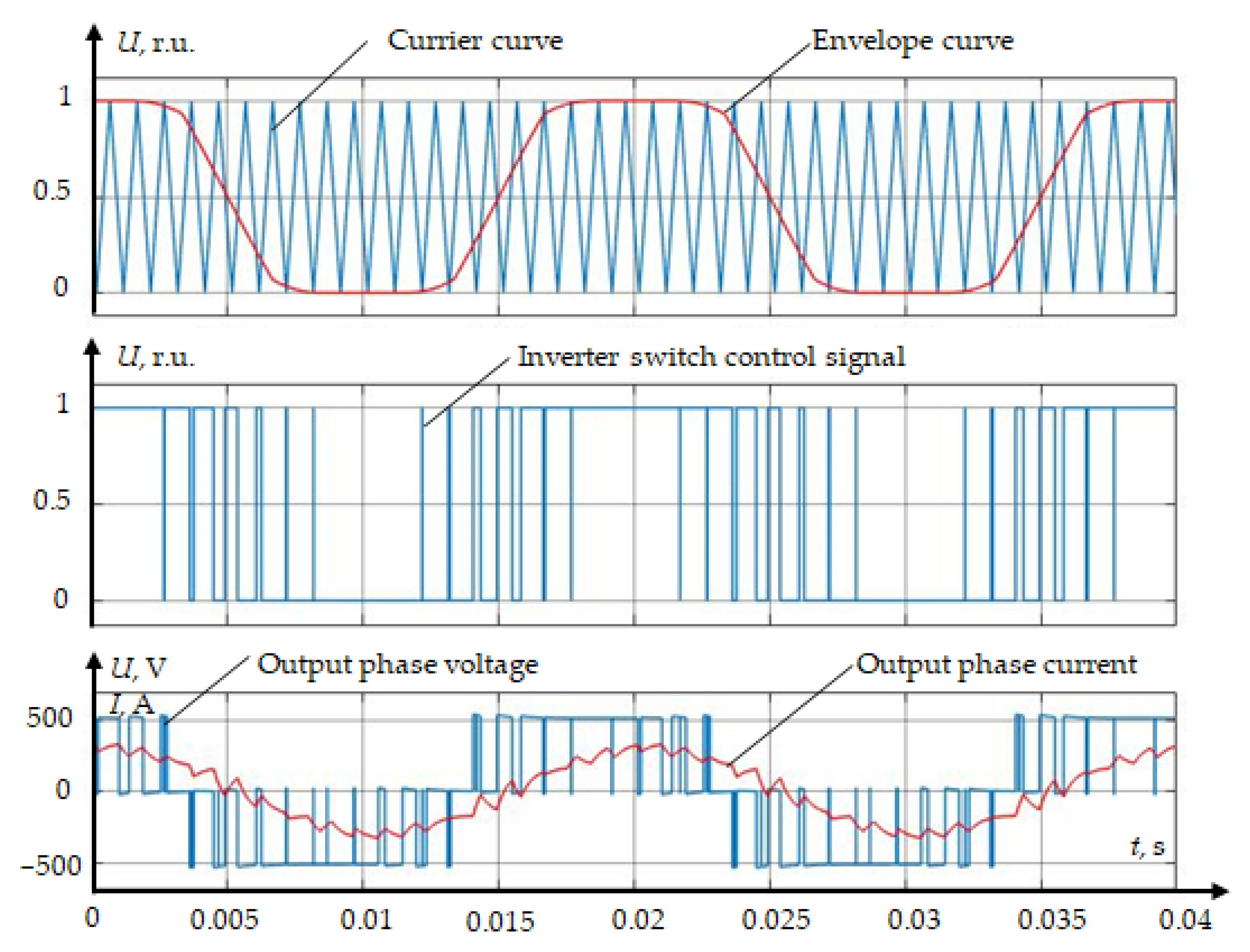
3. Simulation Model of the Proposed Control

To test the proposed ADPWM control method, a three-phase voltage source inverter and its control system Simulink-model was designed. The Simulink-model layout is shown in Figure 3.
The main part of the Simulink-model is a three-phase two level voltage inverter, which is controlled according to the proposed method. The inverter powers a three-phase symmetrical active-inductive load (R = 22 Ohms, L = 8 mH). The inverter is powered by a stabilized 540 V DC link. A three-phase voltage system is formed at the inverter output. The “Three-Phase V-I Measurement” unit measures phase voltages and currents and transfers this information to the measurement system using “OUT_Vabc” and “OUT_Iabc” labels.
The inverter control system unit is shown in Figure 4.
The Simulink-model of the inverter control system unit (Figure 4) generates inverter switch control pulses according to the developed ADPWM algorithm as well as SVPWM, PCDPWM, NCDPWM strategies. The adopted value of PWM carrier frequency is 4000 Hz. The adopted value of output voltage frequency is 50 Hz.
The Simulink-model of the measurement system unit was used to calculate and record simulation data as shown in Figure 5.
Figure 6 shows the flowchart which was used to determine the number of transistor switches.
Transistor control pulses are received by the input of the circuit. Following this, “Detect rise positive” unit detects the control pulse origin. “En” block determines the moment when the pulses start to be counted in order for all transition processes to be finished in the system. “Sum” and “Memory” blocks serve as counting mechanisms.

4. Simulation Results and Discussion

Using the Simulink-model the efficiency of the proposed ADPWM method was studied as compared to CPWM, PCDPWM and NCDPWM methods.
To determine root-mean square value the formula was used:
U R M S ( t ) = 1 T o u t t T o u t t u ( t ) 2
where URMS—is the root mean square value of the measured parameter; TOUT—is the output voltage period TOUT = 1/fOUT (fOUT = 50 Hz); U(T)—is the instantaneous value of the measured parameter.
To determine total harmonic distortion of the measured parameter the formula was used:
T H D = 100 U 2 R M S 2 + U 3 R M S 2 + + U 40 R M S 2 U R M S 2
To calculate dynamic losses in the inverter switches under various PWM strategies the following formula was used:
PINV = (6 · ETS · N)/tP,
where PINV—is dynamic losses in the inverter switches (W); ETS—is the power loss given off in the switch in a single switching cycle (J); tP—is the pulse recording time (s); N—is the number of switches during the recording time.
To determine ETS parameter IRG4PH30KDPBF transistor passport data were used. According to passport ETS = 2.1 mJ.

4.1. Comparing the Performance of the Proposed ADPWM Method with CPWM

The comparison between the proposed ADPWM method and CPWM has been made when operating a three-phase voltage source inverter. To simulate the proposed ADPWM method the following temperature settings were taken: TMIN = 60 °C and TMAX = 100 °C. Figure 7, Figure 8 and Figure 9 show envelope curves, switch control signals, output phase voltage and current generated by the proposed ADPWM method at 1 kHz carrier frequency and modulation index equal to 1. The inverter load is resistor-inductive (R = 1 Ohm and L = 0.5 mH).
The simulation results are shown in Table 1.
The inverter was controlled by CPWM method at radiator temperature below 60 °C (Figure 7). In this case, the number of switches of A phase upper switch was 20 during the period of the inverter output voltage (0.02 s). THD of the load current was 12.7%. The dynamic loss power (PINV) calculated by Formula (7) was 12.6 W.
At 80 °C radiator temperature the inverter was controlled by the ADPWM method (Figure 8). The number of switches of A phase upper switch decreased to 13 for the period of output voltage (0.02 s). THD of the load current increased to 12.78%. The dynamic loss power (PINV) was 8.19 W.
At 100 °C radiator temperature the inverter was controlled by the ADPWM method (Figure 9). The number of switches of A phase upper switch decreased to 7 for the period of output voltage (0.02 s). THD of the load current increased to 13.2%. The dynamic loss power (PINV) was 4.41 W.
The simulation results showed that the proposed ADPWM method reduced dynamic losses in the inverter switches by 2.86 times compared to CPWM, with an increase in the coefficient of nonlinear distortion in the current curve by 0.5%.

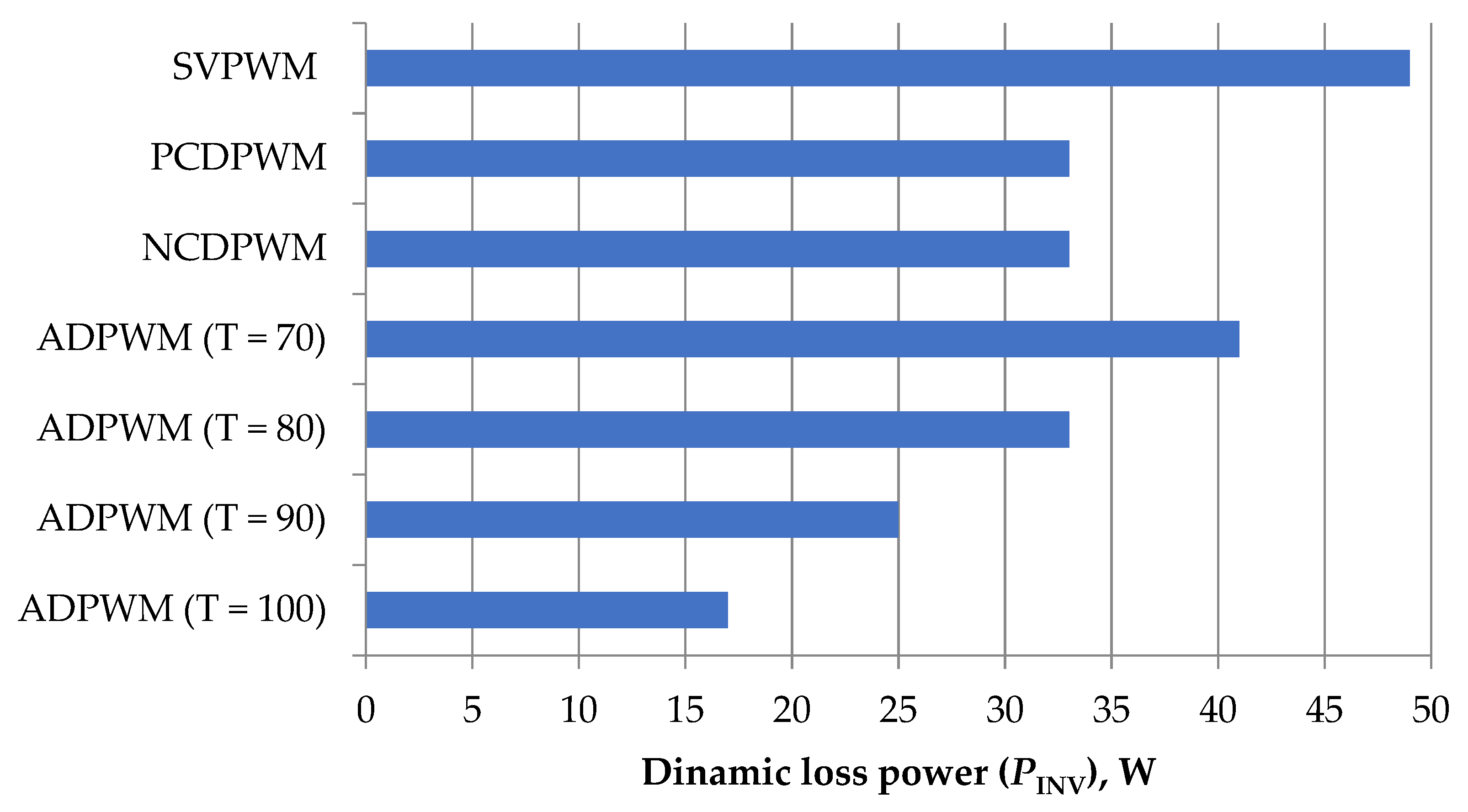
4.2. Comparing the Performance of the Proposed ADPWM Method with PCDPWM and NCDPWM

The comparison between the proposed ADPWM method with PCDPWM and NCDPWM was made when operating a three-phase voltage source inverter at various radiator temperature values and modulation index MI. As soon as at low MI values under DPWM strategy significant distortions in the generated voltages and currents are observed relative to CPWM, MI values from 0.5 to 1 were adopted for the modelling. PWM carrier frequency was adopted as equal to 4 kHz. The simulation results are shown in Table 2, Table 3, Table 4, Table 5, Table 6 and Table 7.
Dynamic losses in the inverter switches dependence for the proposed ADPWM method and other PWM strategies is shown in Figure 10. The load current total harmonic distortion coefficient (THDI) dependence on modulation index (MI) is shown in Figure 11.
The obtained results showed that the proposed ADPWM method reduced the number of transistor switches from 79 (CPWM) to 28 for the period of the output voltage (0.02 s). At the same time, the dynamic losses decreased from 49.77 W to 17.64 W. The proposed ADPWM method allowed to reduce the number of transistor switches by 1.89 times compared to DPWM strategies for the temperatures above 80 °C. Dynamic losses in the inverter switches also decreased by 1.89 times. However, the load current total harmonic distortion coefficient under ADPWM method is higher compared to other DPWM strategies.
Besides, at angles of connection less than 60 el. degrees (at temperature below 80 °C), a significant increase in the load current THD is observed. At this point, the number of switches is higher compared to PCDPWM and NCDPWM methods. Therefore, in further modification of the proposed method the angles of connection less than 60 el. degrees will not be used. The considered 60–100 °C temperature range was chosen as an example and can be adjusted at any time.
The main task of the presented method was to stabilize the temperature of the inverter by reducing dynamic losses. The THD will increase when the shape of the envelope curve changes. The idea of an adjustable transition from CPWM to DPWM is that there should be a smooth decrease in dynamic losses and smooth increase in THD.
It should be noted that the proposed ADPWM method shows the highest efficiency during the voltage inverter operation on the resistance-inductive load (without pre-filters). The most promising area of the proposed ADPWM method application is the electric drives based on medium- and high-power AC motors. This approach can be useful in the mode of short-term overload of the electric motor. In this case, there is an increase in current, which leads to a thermal overload of both the motor and the inverter. In practice, the heating time constant of the motor is much longer than that of the inverter. Therefore, the inverter fails faster. However, the application of the presented ADPWM method will allow for the excess thermal overload of the inverter to be removed, thereby facilitating its operation in the described mode.

5. Conclusions

In order to improve inverter efficiency, it is important to reduce dynamic losses in the inverter switches and total harmonic distortion coefficient. These tasks are solved by applying continuous PWM (CPWM) and discontinuous PWM (DPWM) strategies. However, both groups of strategies have disadvantages. CPWM strategies reduce the total harmonic distortion coefficient, while DPWM strategies provide more efficient reduction of dynamic losses.
The article presents the adjustable discontinuous pulse width modulation (ADPWM) method, which provides an adjustable transition from PWM space vector (refers to CPWM strategies) to DPWM in all inverter phases when the switch temperature exceeds the allowable value in at least one of inverter phases.
A flowchart explaining the principle of the proposed ADPWM method is presented and the modification algorithm for the envelope curve within one sector is shown. The proposed ADPWM method principle is that the inverter switches number reduction when the inverter radiator temperature exceeds the allowable value.
The Simulink-model was developed to generate inverter switches control pulses according to the developed ADPWM method, as well as in accordance with the CPWM, PCDPWM and NCDPWM strategies. The Simulink-model-based research showed that the proposed ADPWM method reduced dynamic losses in the inverter switches by 2.86 times compared to CPWM and by 1.89 times compared to PCDPWM and NCDPWM methods. At the same time, the load current total harmonic distortion coefficient was higher compared to other methods.
Future work:
  • testing the proposed ADPWM method using a three-phase voltage source inverter to verify the data obtained during the simulation;
  • studies of the method operation as closed voltage circuit part.

Author Contributions

Conceptualization, A.D.; methodology, A.D. and V.S.; validation, A.S. (Andrey Shalukho); formal analysis, I.B.; investigation, A.S. (Anton Sluzov) and V.S.; writing—original draft preparation, A.S. (Andrey Shalukho); writing—review and editing, A.D., A.S. (Anton Sluzov) and I.B.; visualization, A.S. (Anton Sluzov); supervision, A.S. (Andrey Shalukho); project administration, A.D. All authors have read and agreed to the published version of the manuscript.

Funding

The reported study was funded by Autonomous Nonprofit Organization “Nizhny Novgorod Research and Educational Center” and “Russian Railways”, project number 33/22/2572 dated 4 May 2022.

Conflicts of Interest

The authors declare no conflict of interest.

Abbreviations

ADPWMAdjustable discontinuous pulse width modulation
CPWMContinuous pulse width modulation
DPWMDiscontinuous pulse width modulation
NCDPWMDPWM strategy with clamping to negative bus bar the number of commutations
PCDPWMDPWM strategy with clamping to positive bus bar the number of commutations
PWMPulse width modulation
SPWMSinusoidal pulse width modulation
SVPWMSpace vector pulse width modulation
THDTotal Harmonic Distortion

References

  1. Abramov, B.I.; Derzhavin, D.A.; Churikov, A.M.; Novoselov, Y.B.; Suslov, M.; Shevyrev, Y.V. Instrumental studies of the electrical energy quality for oil field under conditions of widespread application of frequency-regulated electrical drives. Oil Ind. J. 2016, 1, 90–92. [Google Scholar]
  2. Hava, A.M.; Kerkman, R.J.; Lipo, T.A. A high-performance generalized discontinuous PWM algorithm. IEEE Trans. Ind. Appl. 1998, 34, 1059–1071. [Google Scholar] [CrossRef] [Green Version]
  3. Li, K.; Wei, M.; Xie, C.; Deng, F.; Guerrero, J.M.; Vasquez, J.C. Triangle Carrier-Based DPWM for Three-Level NPC Inverters. IEEE J. Emerg. Sel. Top. Power Electron. 2018, 6, 1966–1978. [Google Scholar] [CrossRef] [Green Version]
  4. Nguyen, T.D.; Hobraiche, J.; Patin, N.; Friedrich, G.; Vilain, J.P. A Direct Digital Technique Implementation of General Discontinuous Pulse Width Modulation Strategy. IEEE Trans. Ind. Electron. 2011, 9, 4445–4454. [Google Scholar] [CrossRef]
  5. Schonung, A. Static frequency changers with subharmonic control in conjunction with reversable variable speed AC drives. Brown Boveri Rev. 1964, 555, 577. [Google Scholar]
  6. Xue, Y.; Li, Y.; Zhang, J.; Lin, J.; Yang, J.T. Application and Simulation of SVPWM Control Techniques in Three-Phase PV Grid-Connected Inverter. Appl. Mech. Mater. 2013, 415, 81–88. [Google Scholar] [CrossRef]
  7. Asiminoaei, L.; Rodriguez, P.; Blaabjerg, F. Application of Discontinuous PWM Modulation in Active Power Filters. IEEE Trans. Power Electron. 2008, 4, 1692–1706. [Google Scholar] [CrossRef]
  8. Mukherjee, S.; Giri, S.K.; Banerjee, S. A modified DPWM scheme for capacitor voltage balancing in three level NPC traction inverter for electric vehicles. In Proceedings of the 2016 IEEE International Conference on Power Electronics, Drives and Energy Systems (PEDES), Thiruvananthapuram, India, 14–17 December 2016. [Google Scholar]
  9. Yang, Z.; Zeng, J.; Ren, Q.; Wu, L.; Liao, Z. A Semi Discontinuous PWM Method for Mitigating Oscillation in a Three-level Grid-tied PV Inverter. In Proceedings of the 2021 IEEE Energy Conversion Congress and Exposition (ECCE), Vancouver, BC, Canada, 10–14 October 2021. [Google Scholar]
  10. Zhang, Z.; Thomsen, O.C.; Andersen, M.A.E. Discontinuous PWM modulation strategy with circuit-level decoupling concept of three level neutral-point clamped (NPC) inverter. IEEE Trans. Ind. Electron. 2013, 60, 1897–1906. [Google Scholar] [CrossRef]
  11. Bruckner, T.; Bernet, S.; Guldner, H. The active NPC converter and its loss-balancing control. IEEE Trans. Ind. Electron. 2005, 52, 855–868. [Google Scholar] [CrossRef]
  12. Bhattacharya, S.; Mascarella, D.; Joos, G. Space-vector-based generalized discontinuous pulsewidth modulation for three-level inverters operating at lower modulation indices. IEEE J. Emerg. Sel. Top. Power Electron. 2017, 5, 912–924. [Google Scholar] [CrossRef]
  13. Sun, Y.; Du, C.; Liu, Q.; Zhu, B.; Wu, C. Research on Neutral-Point Balance Control of Three-Level Inverter Based on Hybrid DPWM. In Proceedings of the 2019 IEEE Conference on Industrial Electronics and Applications (ICIEA), Xi’an, China, 19–21 June 2021. [Google Scholar]
  14. McGrath, B.P.; Holmes, D.G.; Lipo, T. Optimized space vector switching sequences for multilevel inverters. IEEE Trans. Power Electron. 2003, 18, 1293–1301. [Google Scholar] [CrossRef]
  15. Choi, U.M.; Lee, H.H.; Lee, K.B. Simple neutral-point voltage control for three-level inverters using a discontinuous pulse width modulation. IEEE Trans. Energy Conv. 2013, 28, 434–443. [Google Scholar] [CrossRef]
  16. Beig, A.; Kanukollu, S.; AlHosani, K.; Dekka, A. Space vector based synchronized three-level discontinuous PWM for medium voltage high power VSI. IEEE Trans. Ind. Electron. 2014, 61, 3891–3901. [Google Scholar] [CrossRef]
  17. Hadj, M.E. DSP based random discontinuous space vector pwm for variable speed electrical drives. In Proceedings of the 2013 15th European Conference on Power Electronics and Applications (EPE), Lille, France, 2–6 September 2013. [Google Scholar]
  18. Anuchin, A.; Aliamkin, D.; Lashkevich, M.; Shpak, D.; Zharkov, A.; Briz, F. Minimization and redistribution of switching losses using predictive PWM strategy in a voltage source inverter. In Proceedings of the 2018 25th International Workshop on Electric Drives: Optimization in Control of Electric Drives (IWED), Moscow, Russia, 31 January–2 February 2018. [Google Scholar]
  19. Anuchin, A.; Briz, F.; Shpak, D.; Lashkevich, M. PWM strategy for 3-phase 2-level VSI with non-idealities compensation and switching losses minimization. In Proceedings of the 2017 IEEE International Electric Machines and Drives Conference (IEMDC), Miami, FL, USA, 21–24 May 2017. [Google Scholar]
  20. Ojo, O. The generalized discontinuous PWM scheme for three-phase voltage source inverters. IEEE Trans. Ind. Electron. 2004, 6, 1280–1289. [Google Scholar] [CrossRef]
  21. Yoo, S.; Lee, J.; Lee, K. Novel Discontinuous PWM Method of a Three-Level Inverter for Neutral-Point Voltage Ripple Reduction. IEEE Trans. Ind. Electron. 2016, 63, 3344–3354. [Google Scholar]
  22. Lee, J.-S.; Kwak, R.; Lee, K.-B. Novel Discontinuous PWM Method for a Single-Phase Three-Level Neutral Point Clamped Inverter with Efficiency Improvement and Harmonic Reduction. IEEE Trans. Power Electron. 2018, 11, 9253–9266. [Google Scholar] [CrossRef]
  23. Zu, G.; Zhu, X.; Yang, S. Using DPWM method to improve system efficiency of the machine drive system. In Proceedings of the 2019 22nd International Conference on Electrical Machines and Systems (ICEMS), Harbin, China, 11–14 August 2019. [Google Scholar]
  24. Lee, H.; Yoo, A.; Hong, C.; Lee, J. A carrier-based adjustable discontinuous PWM for three-phase voltage source inverter. In Proceedings of the 2015 IEEE Energy Conversion Congress and Exposition (ECCE), Montreal, QC, Canada, 20–24 September 2015. [Google Scholar]
  25. Gowri, K.; Reddy, T.B.; Babu, S.; Pulla, G. High-Performance Generalized ADPWM Algorithm for VSI Fed IM Drives for Reduced Switching Losses. Int. J. Recent Trends Eng. 2009, 5, 96–100. [Google Scholar]
  26. Pradeepa, S.; Kumar, S.; Prakash, G. Adoption of SVPWM Technique to CSI and VSI. In Proceedings of the 2018 3rd International Conference for Convergence in Technology (I2CT), Pune, India, 6–8 April 2018. [Google Scholar]
Figure 1. Flowchart of the developed three-phase voltage source inverter control method: 1—sector determining unit; 2—angle inside the sector determining unit; 3—time evaluation unit of base vector connection and the pause time; 4—phase voltage envelope curve calculating unit; 5—phase voltage envelope curve modification unit; 6—angles of connection calculating unit; 7—switch control pulse-generating unit; 8—PWM triangular reference voltage shaping unit.
Energies 15 07463 g001
Figure 2. The flowchart of modification algorithm of envelope curve inside sector 1.
Energies 15 07463 g002
Figure 3. Simulink-model to test the proposed control method.
Energies 15 07463 g003
Figure 4. Simulink-model of the inverter control system unit.
Energies 15 07463 g004
Figure 5. Simulink-model of the measurement system unit.
Energies 15 07463 g005
Figure 6. Flowchart to determine the number of transistor switches.
Energies 15 07463 g006
Figure 7. Simulation results at 0 electrical degrees angle of connection (T = 60 °C and below).
Energies 15 07463 g007
Figure 8. Simulation results at 60 electrical degrees angle of connection (T = 80 °C).
Energies 15 07463 g008
Figure 9. Simulation results at 120 electrical degrees angle of connection (T = 100 °C).
Energies 15 07463 g009
Figure 10. Dynamic losses in the inverter switches dependence for the proposed ADPWM method and other PWM strategies.
Energies 15 07463 g010
Figure 11. THDI on MI dependence for the proposed ADPWM method and other PWM strategies at various inverter radiator temperatures.
Energies 15 07463 g011
Table 1. Simulation results comparing CPWM and proposed ADPWM method.
CPWMADPWM
(T = 70 °C)
ADPWM
(T = 80 °C)
ADPWM
(T = 90 °C)
ADPWM
(T = 100 °C)
N201614107
URMS,B239.3241.6241.9242.2245
IRMS,A209.1214.1214.6215218.8
THDU,%54.7251.3851.0951.0349.55
THDI,%12.7912.7512.7812.8913.25
Psw,W12.610.088.826.34.41
Table 2. Simulation results at MI = 0.5.
PCDPWMNCDPWMADPWM
(T = 60 °C)
ADPWM
(T = 70 °C)
ADPWM
(T = 80 °C)
ADPWM
(T = 90 °C)
ADPWM
(T = 100 °C)
N53537966534028
URMS,B176.7174.6175.7199.5219.2236.6254.7
IRMS,A5.0114.9824.9536.6097.8759.02610
THDU,%123.5126.1124.594.9976.0263.357.97
THDI,%10.9210.966.12820.1310.8710.5912.4
Table 3. Simulation results at MI = 0.6.
PCDPWMNCDPWMADPWM
(T = 60 °C)
ADPWM
(T = 70 °C)
ADPWM
(T = 80 °C)
ADPWM
(T = 90 °C)
ADPWM
(T = 100 °C)
N53537966534028
URMS,B193.3191.5192.2210.5225.9239.6254.5
IRMS,A5.9925.9645.937.2878.3229.24810.06
THDU,%105.1107.4106.385.1170.5760.4256.09
THDI,%9.2089.2625.49815.559.0318.56910.5
Table 4. Simulation results at MI = 0.7.
PCDPWMNCDPWMADPWM
(T = 80 °C)
ADPWM
(T = 90 °C)
ADPWM
(T = 100 °C)
ADPWM
(T = 110 °C)
ADPWM
(T = 120 °C)
N53537966534028
URMS,B208.4207.1207.3220.6231.5242.2253.8
IRMS,A6.9936.9446.9377.9878.7689.46910.11
THDU,%90.2691.5391.2476.3365.9558.7954.51
THDI,%7.5427.6214.95911.437.3277.0468.784
Table 5. Simulation results at MI = 0.8.
PCDPWMNCDPWMADPWM
(T = 80 °C)
ADPWM
(T = 90 °C)
ADPWM
(T = 100 °C)
ADPWM
(T = 110 °C)
ADPWM
(T = 120 °C)
N53537966534028
URMS,B222.4221.4221.7231.1238.2245.4254
IRMS,A7.9677.9627.9318.7029.2379.71310.19
THDU,%76.9477.9477.6267.360.4555.6252.44
THDI,%6.1166.1774.5518.3986.0555.5847.185
Table 6. Simulation results at MI = 0.9.
PCDPWMNCDPWMADPWM
(T = 80 °C)
ADPWM
(T = 90 °C)
ADPWM
(T = 100 °C)
ADPWM
(T = 110 °C)
ADPWM
(T = 120 °C)
N53537966534028
URMS,B235.9234.9235240.9244.5248.4253.9
IRMS,A8.9658.9188.9149.4159.79.95910.27
THDU,%64.3865.1765.0758.5554.9452.3150.33
THDI,%4.9675.0124.3136.1475.1784.6865.912
Table 7. Simulation results at MI = 1.0.
PCDPWMNCDPWMADPWM
(T = 80 °C)
ADPWM
(T = 90 °C)
ADPWM
(T = 100 °C)
ADPWM
(T = 110 °C)
ADPWM
(T = 120 °C)
N53537966534028
URMS,B248.3247.7247.6250.3250.8251.4254
IRMS,A9.9399.9029.89610.1310.1810.2110.35
THDU,%52.4953.0153.0449.949.3148.9748.18
THDI,%4.4014.4034.2634.794.74.6185.241
Publisher’s Note: MDPI stays neutral with regard to jurisdictional claims in published maps and institutional affiliations.

