Article

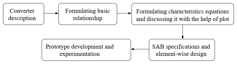
An Analysis-Supported Design of a Single Active Bridge (SAB) Converter

1
School of Electrical Engineering, Dr. Vishwanath Karad MIT World Peace University, Pune 411038, India
2
Electrolux Italia S.p.A., Susegana, 31025 Treviso, Italy
3
Department of Electrical Engineering, Zeal College of Engineering & Research, Pune 411041, India
4
KPIT Technologies Ltd., Pune 411057, India
5
Department of Industrial Engineering, University of Padova, 35131 Padova, Italy
*
Authors to whom correspondence should be addressed.
Energies 2022, 15(2), 666; https://doi.org/10.3390/en15020666
Submission received: 29 December 2021 / Revised: 6 January 2022 / Accepted: 10 January 2022 / Published: 17 January 2022
(This article belongs to the Collection Electrical Power and Energy System: From Professors to Students)

Abstract

:
Currently, due to its various applications, the high-performance isolated dc-dc converter is in demand. In applications where unidirectional power transfer is required, the single active bridge (SAB) is the most suitable one due to its simplicity and ease of control. The general schematic of the SAB converter consists of an active bridge and a passive bridge, which are connected through a high-frequency transformer thus isolated. The paper summarizes the behavior of this converter in its three operation modes, namely the continuous, discontinuous, and boundary modes. Later, the features of this converter, such as its input-to-output and external characteristics are discussed. Input-to-output characteristics include the variation of converter output power, voltage, and current with an input control variable i.e., phase-shift angle, whereas the external characteristic is the variation of the output voltage as a function of output current. In this discussion, the behavior of this converter in its extreme operating conditions is also examined. The features of the characteristics are elucidated with the help of suitable plots obtained in the MATLAB environment. Afterward, the specifications of a SAB converter are given and, based on the results of the analysis, a detailed design of its electrical elements is carried out. To validate the features and the design procedures presented in this paper, a prototype is developed. An element-wise loss estimation is also carried out and the efficiency of the converter has been found to be approximately equal to 93%. Lastly, the test was executed on this prototype, confirming the theoretical findings concerning this converter.

1. Introduction

In todays’ applications, isolated dc-dc converters are becoming more prevalent. Their main advantages include a compact structure, galvanic isolation, and excellent efficiency [1,2,3,4,5,6]. A variety of converters exist; of these the dual active bridge (DAB) [7,8,9], single active bridge (SAB) [10,11], semi-DAB [12,13], and phase shift full bridge (PSFB) [14,15,16] are the most commonly used isolated dc-dc converters. Resonant dc-dc converters such as LLC [17], CLLC [18,19], and LC [20,21] are also popular due to their virtues of soft switching and better efficiency. However, the resonant converters are out of the scope of this paper and are not discussed hereafter.
Figure 1 shows the general schematic of an isolated dc-dc converter. Bridge 1 is usually of the active kind and is utilized in all types of dc-dc converters. In contrast, bridge 2 is of different types; for the DAB converters, it is of the active type and the bridge sides are composed of controlled switches; for the SAB converter, it is a passive type and the bridge sides are composed of diodes; for the semi DAB converters, the bridge sides are a combination of controlled switches and diodes [13]; for the PSFB, for unidirectional application, it is a diode rectifier [14,15] and, for bidirectional application, it is of the active type with a clamping diode in bridge 1 [16]. Moreover, the PSFB converter contains an inductor at the output of bridge 2. The schematic in Figure 1 includes, besides the two bridges, the following elements: (i) the inductor L, which accounts for the total leakage inductance of the isolation transformer, (ii) the capacitor Co, which filters the output voltage Vo, and (iii) the resistor Rl, which represents the load of resistive nature.
For applications where unidirectional power transfer is required, PSFB and SAB are suitable. As mentioned earlier, the PSFB converter constitutes a reactor at the output. This converter can realize a unity voltage conversion ratio, as the reactor is bulky, and can operate in a continuous current mode. Furthermore, due to the surge voltage generated by the reactor and the parasitic capacitor of the diode rectifier, high voltage diodes must be used to realize the diode rectifier [22]. However, refs. [23,24] have suppressed the voltage surge with the use of an auxiliary circuit. As an alternative, moving the reactor to the primary side of the converter can reduce the inductance by a factor of the square of the transformer turn-ratio. Furthermore, this external inductor can also be realized by the leakage inductance of the transformer; thus, no extra inductor is needed. This topology is referred to as the SAB.
Since bridge 2 of the SAB converter consists of diodes only, this is the most convenient converter among the unidirectional converters in terms of simplicity. This bridge 2 configuration not only decreases the cost and volume of a dc-dc converter but may also be utilized in a series connection to obtain a dc-dc converter with a medium-voltage rating. Furthermore, it simplifies SAB converter control, making the SAB a very appealing alternative for unidirectional power flow applications. The possibility of its use for power transmission from an offshore wind farm to the onshore network via a high voltage DC system has also been demonstrated in [25].
Existing literature on the SAB converters is mainly focused on topologies with half-bridge (HB) or full-bridge (FB) input, and deals with either their working principles or soft-switching capabilities of the transistors or other specific aspects [10,11,26,27,28,29,30,31]. Specifically, in [10], the dynamics and basic working principle of an HB SAB converter are presented; in [11], the switching losses of the transistors of an FB SAB converter were mitigated by employing a dual-current pulse control; in [26], the snubber capacitor is optimized to improve the FB SAB converter efficiency; in [27], a partial-resonant FB SAB converter is arranged for the reduction of the transistor conduction losses; in [28], an open-circuit fault detection method and the tolerant control strategy for N parallel-connected FB SAB converters are reported; in [29], the impact of transformer turns ratio and leakage inductance on the operating behavior of the FB SAB converter with a voltage doubler is studied, where one leg of the bridge 2 diode rectifier is replaced with two capacitors; in [30,31], respectively, the design characteristics and soft-switching capabilities of an FB SAB converter are compared to those of the DAB converter.
There are numerous papers available that deal with the functioning, design, and control of dc-dc converters. In [32], the design and performance analysis of a 6 kW DAB converter utilized to charge a Li-ion battery-based storage system are discussed; in [33], operational principles and design guidelines are exposed for a three-phase SAB converter; in [34], the design and control of a 10 kW DAB converter are presented, preceded by a study of its behavior in different modes of operation; in [13], a 1 kW semi-DAB converter is analyzed and its performance is documented, including its ZVS capabilities; in [35], a 10 kW three-phase DAB is designed and developed; in [36] a 1400 W PSFB converter for server applications is developed; and in [14], a PSFB converter of 350 W is designed and implemented. Despite the fact that there is substantial literature on dc-dc converters, there are no articles that address the characteristics of the SAB converter with two full bridges and how to design its elements. In this regard, the purpose of this paper is to encompass such issues. The objectives of this paper and the methodology used are as follows. The paper starts by summarizing the working principle of the SAB converter at a steady state in its three operation modes, namely continuous, discontinuous, and boundary modes. It should be noted that a similar study is also presented in [30] but, to discuss the SAB converter characteristics and its design procedure, which is the novel part of this paper, it is necessary to formulate some basic relationship, to be included in the paper. Since there is only one control parameter in this converter, called the phase-shift angle, it is a matter of interest to observe how the output parameters such as output power, voltage, and current vary with respect to the phase-shift angle. The relationship of the output quantities with the phase-shift angle, as mentioned earlier, is termed here as the input-to-output characteristics of the converter. Moreover, another important observation where the output voltage is plotted against output current is also included here and termed as the converter external characteristic. The external characteristic is very useful to locate the converter operating point and subsequently detect the corresponding operation mode. The same characteristic is also useful to examine converter behavior in extreme operating conditions. These characteristics are first formulated and later plotted in the MATLAB environment and then elaborated to provide design hints.
From the design perspective, the specifications of this converter are specified. It should be noted that the design specifications do not target any particular application, but are incorporated here to validate the simulation findings. However, a similar approach can be used to design this converter for any power ratings. Later, the element-wise design is included in the paper followed by the losses associated with the individual elements and calculation of the overall converter efficiency. Based on the specifications and design approach, a SAB prototype is developed and put to the test. Finally, the experimental results are also encompassed in the paper. Figure 2 includes the used methodology for the paper.
The organization of this paper is as follows. Section 2 describes the basic circuit of the SAB. Section 3 studies its three operational modes. Section 4 and Section 5 include the characteristics and element-wise design, respectively. Section 6 includes the experimental results and Section 7 concludes the paper.

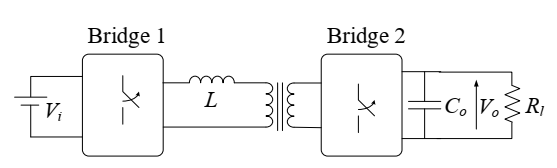
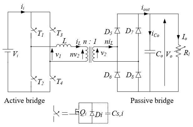
2. SAB Converter Description

As shown in Figure 3, the circuit diagram of a SAB converter is composed of two bridges coupled through a transformer. Bridge 1, also known as the input bridge, is an active-type bridge that is powered by the DC voltage Vi. It functions as an inverter and generates the AC high-frequency voltage v1 at its output. The active bridge’s switches Ti are made up of two elements (transistor Qi and freewheeling diode Di) as well as a snubber circuit Cs,i. Transistor Qi might be a MOSFET or an IGBT for medium- and high-power applications. The snubber circuit is used to soft-switch Qi, while the diode Di permits negative current to flow through Ti. The output bridge of the SAB converter is a passive bridge that is powered by voltage v2 at the isolation transformer’s secondary. The bridge functions as a pure rectifier and, in conjunction with the filtering effect of Co, produces the dc voltage Vo at the output of the SAB converter.

3. SAB Converter Analysis

Depending on the current in the inductor L, three operation modes can occur for the SAB converter, yielding peculiar sets of equations relating the output quantities to the input ones. Therefore, each mode is analyzed separately. The equations are formulated under the following hypotheses: (i) the turns ratio n of the isolation transformer is equal to 1, (ii) its magnetization inductance is large enough to make the magnetizing current negligible, and (iii) Co is large enough to make the ripple of the output voltage Vo negligible.
Waveforms of voltages and currents for the three operation modes are plotted in Figure 4 as a function of the angular quantity θ , which is proportional to the time according to θ = ω s t ; quantity ω s is the working angular frequency in rad/sec of the SAB converter and is given by 2π/Ts, where Ts is the working period. The phase-shift angle between the driving of the two transistors on the same side is designated with β and ranges from 0 to π. The two sets of waveforms at the top of Figure 4 show the voltage v1 at the output of the active bridge and the voltage v2 at the input of the passive bridge. The two sets at the bottom of Figure 4 show the current iL in the inductor L and the current iout at the output of the passive bridge.
Looking at the waveforms, it emerges that they exhibit the odd symmetrical property with respect to π.

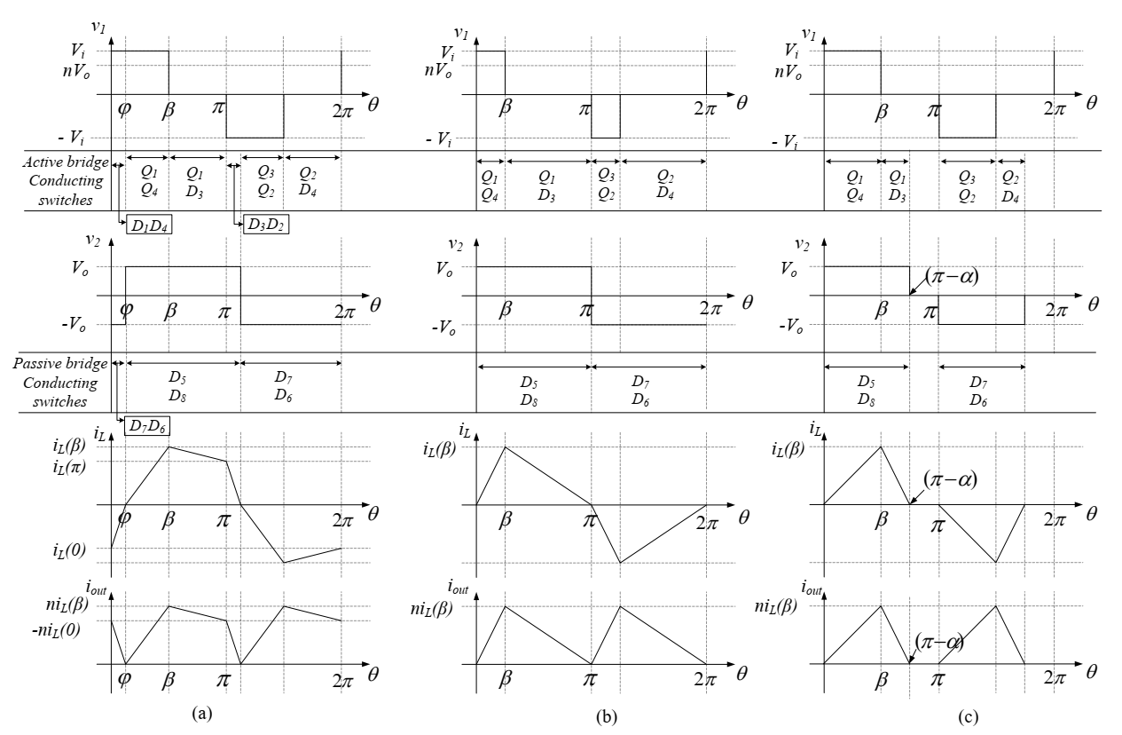
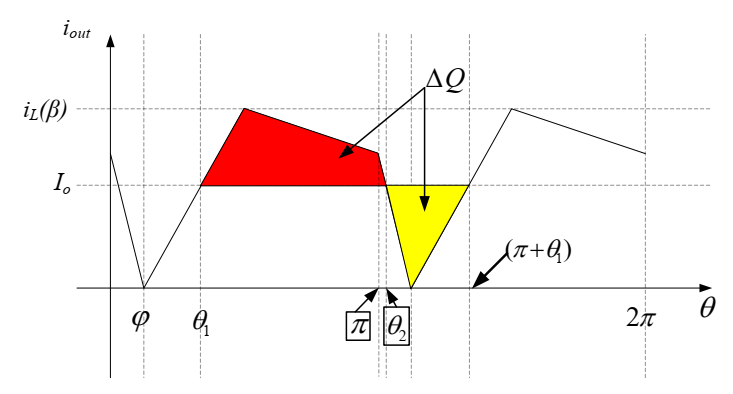
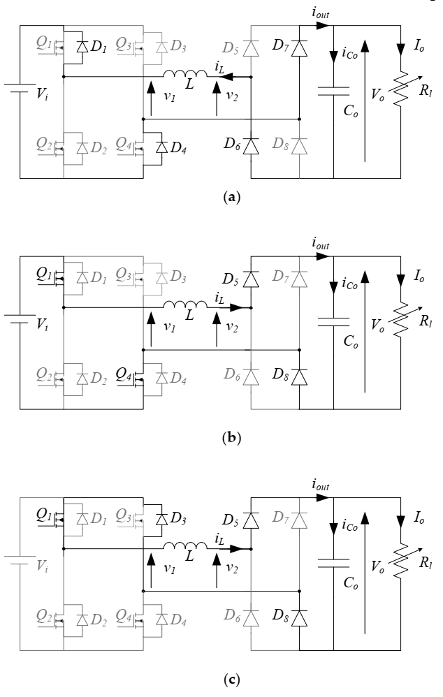
3.1. Continuous Conduction Mode

The circuit analysis is simplified by replacing the transformer with a leakage inductance L. A pair of output bridge diodes conduct at any moment in the Continuous Conduction Mode (CCM). Then, the voltage v2 can be either Vo or −Vo depending on the sign of the current iL. The waveforms of voltages and currents in CCM are presented in Figure 4a, showing that the voltage v1 has a quasi-square waveform, whereas the voltage v2 has a pure square waveform with the same zero crossings as the current iL; the delay angle of v2 to v1 is indicated with φ. The current iL, in turn, has a linear piecewise waveform, which is forced by the voltage v L applied to the terminals of the inductor L. Such voltage is given by ( v 1 v 2 ) and has a piecewise constant waveform, made up of the three intervals [0 ÷ φ], [φ ÷ β] and [β ÷ π] within the half-period [0 ÷ π]. The equations of v l and iL in the three intervals are as follows:

3.1.1. Interval 1

Span of Interval 1 is [0 ÷ φ]. Figure 5a depicts the currents paths and devices conduction in this interval. The voltage vL is equal to (Vi + Vo), and the current iL grows linearly from iL(0) until it vanishes at θ = φ ; the expression of the current at φ is
i L φ = i L 0 + V i + V o ω s L φ 0

3.1.2. Interval 2

Span of Interval 2 is [φ ÷ β]. Figure 5b depicts the currents paths and devices conduction in this interval. The voltage vL is equal to (Vi − Vo), and the current iL grows linearly from 0 to its peak value, which is reached at θ = β ; the expression of the peak current is
i L β = i L φ + V i V o ω s L β φ

3.1.3. Interval 3

Span of Interval 3 is [β ÷ π]. Figure 5c depicts the currents paths and devices conduction in this interval. The dc voltage source Vi does not feed the inductor L, and the voltage vL is equal to −Vo; then, the current iL drops linearly and its expression at θ = π is
i L π = i L β V o ω s L π β
By the odd symmetrical property, the current i L π is equal to i L 0 .
The average value of vL in the interval [ φ ÷ π +   φ ] is zero since the current iL takes the same value, equal to zero, at the two extremes of the interval. It follows that
V o V i = β 2 φ π
As Vo is a positive value, Equation (4) reveals some basic properties of the SAB converter operation in CCM. Firstly, 2 φ is lower than β . Secondly, Vo is lower than Vi and this indicates that the SAB converter works as a step-down converter. Thirdly, it is
V o V i < β π
The Equation (5) is the distinctive condition for the SAB converter to operate in CCM.
By obtaining φ from Equation (4) and substituting it in Equations (1) and (3), the expressions of the current i L at 0 and β can be written as a function of the input and output voltage, Vi and Vo, and the phase-shift angle β. It is
i L 0   = V i 2 ω s L 1 + V o V i β V o V i π
i L β   = V i 2 ω s L 1 V o V i β + V o V i π

3.2. Boundary Conduction Mode

The Boundary Conduction Mode (BCM) separates CCM from the Discontinuous Conduction Mode (DCM). It stands out because the current iL becomes zero exactly when θ =   0, and then when θ = π . The waveforms of voltages and currents in DCM are plotted in Figure 4b and show that, in the half-period [0 ÷ π], the voltage vL is equal to ViVo from 0 to β and to −Vo from β to π. If the average value of vL, in this half-period, is equal to zero, we obtain
V o V i = β π
Equation (8) is the distinctive condition for the SAB converter to operate in BCM. It discloses that, for an equal value of the input voltage Vi and phase-shift angle β, the voltage Vo in BCM is higher than in CCM.
The peak value of the current iL is given by
i L β = V i ω s L 1 β π β

3.3. Discontinuous Conduction Mode

In the DCM, the current iL does not flow within an interval in the half-period [0 ÷ π]. The waveforms of voltages and currents in DCM are plotted in Figure 4c and show that the current iL is zero from [πα] to π. Within this interval, also the voltage v2 is zero because all four diodes of the passive bridge remain reverse biased.
Moreover, the voltage vL is equal to ViVo from 0 to β and to −Vo from β to [πα]. If the average value of vL in the half-period is equal to zero, then
V o = V i β π α
Since [ π α ] is greater than β , Equation (10) reveals that, like in CCM, Vo is lower than Vi, and the SAB converter works again as a step-down converter. From Equation (10) it follows that
V o V i > β π
Equation (11) is the distinctive condition for the SAB converter to operate in DCM. The expression of the peak of the current iL is still given by Equation (9).

4. SAB Converter Characteristics

The input-to-output and external characteristics of the SAB converter can be formulated using the preceding results. The phase-shift angle β, in addition to the voltage Vi, is the input quantity. The voltage Vo, the average value Io of the current iout, and the power Po, given by VoIo, are the output quantities. They represent the voltage across, current into, and power drawn by the load resistor Rl, and are referred to as output voltage, current, and power hereafter.
At steady state, the input-to-output characteristics clearly provide the control characteristics of the SAB converter. The external characteristic is a relationship between the output voltage and the output current; in other words, it describes the SAB converter’s electrical behavior as observed from its output terminals.
The current Io is calculated as the integral of iout over the half-period [0 ÷ π], which takes advantage of the odd symmetrical property of the current iout. Io is given as
I o = 1 π 0 π i o u t θ d θ  
To set forth expressions of general validity, the equations of the characteristics are formulated in terms of “per unit (pu)” quantities. They are worked out in the next subsections and collected in Table 1.

4.1. Per Unit Quantities

Let us define the voltage, current and angle bases as
V b = V i ;   Z b = ω s L ;   θ b = π
By Equation (13), the power and current bases are derived as
P b V b 2 Z b = V i 2 ω s L ;   I b V b Z b = V i ω s L

4.2. CCM

Looking at the graph at the bottom of Figure 4a, the current I o in CCM can be calculated as the sum of the areas of three simple geometrical Figures, namely two triangles and one trapezoid, that extend respectively in the intervals [0 ÷ φ], [φ ÷ β], and [β ÷ π]. Further to the above observation and Equation (4), the expression of I o in pu is formulated as in Equation (15). It follows the expression of Po,pu in Equation (16)The expression of Vo,pu is found by equating Io,pu to Vo,pu/Rl,pu and extracting Vo,pu, thus yielding Equation (17). The latter Equation outlines that, in pu quantities, the output voltage Vo depends only on the phase-shift angle β and the load resistor Rl.
It is of interest to formulate the expression of the load resistor in CCM. By taking the ratio of Vo,pu to Io,pu, one can obtain it as Equation (18).

4.3. BCM

Looking at the graph at the bottom of Figure 4c, the current I o in BCM can be calculated as the area of the triangle that extends in the half-interval [0 ÷ π]. In light of the preceding observation and Equation (8), Io,pu is expressed as Equation (19). It follows the expression of Po,pu in Equation (20) and that of Vo,pu in Equation (21). Note that they all depend only on β.
It would be interesting to define the load resistance expression in BCM as well. By taking the ratio of Vo,pu to Io,pu, one can obtain it as Equation (22).
Table 1. Equations for Output Voltage, Current and Power in the Three Operation Modes.
CCMBCMDCM
I o , p u π 4 2 β p u V o , p u 2 β p u 2   15 π 2 1 β p u β p u   19 π 2 1 V o , p u β p u 2 V o , p u   23
P o , p u π 4 V o , p u 2 β p u V o , p u 2 β p u 2   16 π 2 1 β p u β p u 2   20 π 2 1 V o , p u β p u 2   24
V o , p u 2 π 1 R l , p u + 1 R l , p u 2 + π 2 2 2 β p u β p u     17 β p u   21 π 4 R l , p u β p u 2 1 + 1 + 8 R l , p u β p u 2 π   25
R l , p u 4 π V o , p u 2 β p u V o , p u 2 β p u 2 ( 18 ) 2 π 1 1 β p u ( 22 ) 2 π V o , p u 2 1 V o , p u β p u 2 ( 26 )
It can readily be demonstrated that Equation (22) is greater than Equation (18); this shows that the SAB converter operates in CCM for load resistances lower than Equation (22). Therefore, by Equation (22), when β is close to π, the resistance R l . B C M , p u becomes very high and the SAB converters operate in CCM for any practical load.

4.4. DCM

Looking at the graph at the bottom of Figure 4b, the current I o in DCM can be calculated as the area of the triangle that extends in the half-interval [0 ÷ π − a]. Further to the above observation and Equation (10), the expression of I o , p u is formulated as in Equation (23). It follows the expression of Po,pu in Equation (24) and that of Vo,pu in Equation (24). As before, Equation (25) outlines that, in pu quantities, the output voltage Vo depends only on the angle β and the resistor Rl.
It is of interest to formulate the value of the load in DCM. By taking the ratio of Vo,pu to Io,pu, one can obtain it as Equation (26).
It can readily be demonstrated that Equation (26) is greater than Equation (22); this shows that the SAB converter operates in DCM for load resistances greater than Equation (22). It is worth noting that Equations (18), (22) and (26) on the load resistance are alternatives to Equations (5), (8) and (11) on the output voltage in discriminating between the SAB converter operation modes.

4.5. Characteristic Features
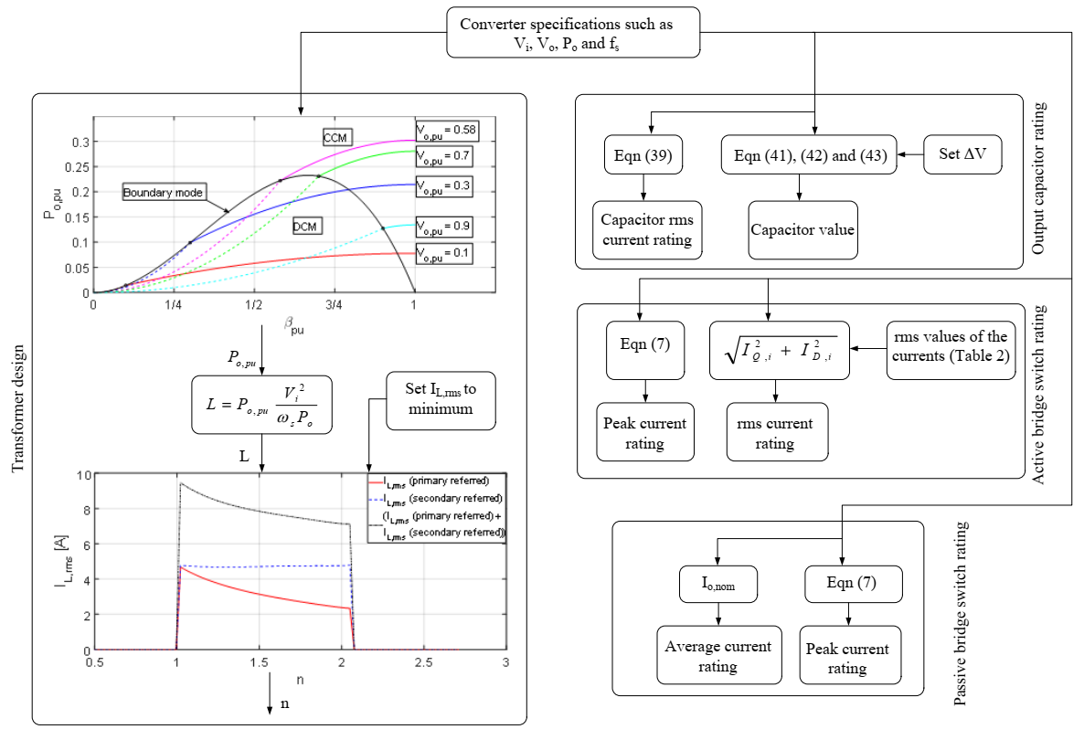
The features of the SAB converter characteristics are elucidated by resorting to some graphs. Let us start by drawing the characteristic that relates the output power to the phase-shift angle in Figure 6, as per Equations (16), (20) and (24). The Figure highlights that the characteristic is composed of a family of curves, each of them distinguished by a different value of the output voltage.
The curves demonstrate that, for a fixed value of V o , p u , the output power increases monotonously with the phase-shift angle so that the maximum output power is reached at βpu = 1, i.e., when the input bridge generates a square-wave voltage, and the SAB converter operates in CCM. What may be surprising is that the highest value of the output power is not achieved when V o , p u is maximum, but when it is equal to 1 / 3 0.58 , being the related power equal to 0.3. In BCM, the highest output power is delivered at βpuVo,pu = 2/3 and is equal to about 0.23, which is 2.5 times less than that in CCM. All these values can be directly computed from Equations (16) and (20). Given that the DCM region extends below the BCM curve, the output power in DCM does not exceed 0.23.
Figure 7 illustrates the characteristic relating the output voltage to the phase-shift angle. It is composed of a family of curves, each of them distinguished by a different value of the load resistor Rl,pu, as per Equations (17), (21), and (25). The main outcome of Figure 7 is that the SAB converter does not behave like a voltage source, since the output voltage changes with the load. Other outcomes of interest are: (i) the output voltage increases with Rl,pu, while still remaining less than 1, and (ii) the output voltage rises nearly proportional to the phase-shift angle for low values of βpu, and with a saturated behavior for βpu approaching 1, (iii) the BCM plot is a straight line, and (iv) the lighter the load, the wider the range of βpu, where the SAB converter operates in DCM.
Figure 8 illustrates the characteristic relating the output current to the phase-shift angle. It is composed of a family of curves, each of them distinguished by a different value of the output voltage, as per Equations (15), (19), and (23). Similarly to Figure 6, Figure 8 shows that, for a fixed Vo,pu, the curves of the output current have an increasing monotonic behavior so that they reach their maximum at βpu = 1, i.e., when the input bridge generates a square-wave voltage and the SAB converter operates in CCM. Differently from Figure 6, the peak value of the output current is reached for Vo,pu = 0, whilst the maxima of the output current decrease as Vo,pu increases. The BCM curve is a parabola, as can be realized from Equation (19).
Figure 9 illustrates the external characteristic of the SAB converter; it is composed of a family of curves relating the output voltage to the output current for different values of the phase-shift angle. The equations of the curves are obtained by (i) substituting Equations (17) and (25) in place of Equations (15) and (23), (ii) tracing Io,pu as a function of Vo,pu, and, lastly, (iii) inverting the graph. The Equation of the BCM curve is found by substituting Vo,pu to βpu in Equation (19), obtaining
I o , p u = π 2 1 V o , p u V o , p u
Equation (27) outlines that, in BCM, Io,pu is a parabolic function of Vo,pu. The curves of Figure 9 highlight that the SAB converter operates in DCM when the working point lies in between the Vo,pu axis and the BCM curve, whereas it operates in CCM when Io,pu is greater than Equation (27), calculated for the actual value of V o , p u . Once again, it can be seen that the SAB converter operates in DCM over a wide range of the output current when it is lightly loaded.
The curves of Figure 9 also reveal two remarkable features of the SAB converter. The first one is that the SAB converter gets the maximum output voltage at no-load; it has a finite value that is equal to 1, irrespective of βpu. The second feature is that the SAB converter gets the maximum output current at short-circuit, with the input bridge generating a square-wave voltage. By replacing βpu = 1 and Vo,pu = 0 in Equation (15), the maximum value of I o turns out to be equal to
I o , p u , M A X = π 4 0.79
Therefore, the SAB converter is built to withstand the extreme working conditions of open or short-circuited output terminals.

5. SAB Design

This section is devoted to the design of the SAB converter by sizing and selecting its circuit elements. Supplementary Equations, which are needed to support the design, are first formulated.

5.1. Design-Supporting Equations

Active Bridge: Besides the voltage solicitation, the sizing of the active bridge switches requires the valuation of the peak and rms values of current flowing through each of them. Let us consider first the value of the peak current.
From the current waveforms reported in Figure 4a,c for the CCM and DCM modes, it emerges that, regardless of the operating mode, the peak of the current circulating in the switches is reached at β and is equal to iL(β). The relationship between iL(β) and the average output current Io of the SAB converter is again obtained with the aid of the p.u. quantities. Equation (7), conveniently scaled by the base current, and Equation (15) are used for this purpose in the case of the CCM operation mode. A similar approach is used for the DCM. Because the resulting expressions are extremely complex, it was thought that exposing them in graphical form would be more beneficial. This is done in Figure 10, where the relationship is plotted for different output voltage values. The Figure emphasizes that the peak current circulating in the switches has an increasing monotonic trend with the current Io. Moreover, from the Figure, it emerges that: (i) as Vo,pu increases, the peak current delivered by the active converter reduces significantly, and (ii) in DCM, the curve piece belonging to Vo,pu = 0.1 coincides with that belonging to Vo,pu = 0.9, and the same is true when Vo,pu is equal to 0.7 and 0.3. The curves also confirm that, as the current Io increases, the operation of the SAB converter swaps from DCM (dashed lines) to CCM (continuous lines).
To complete the analysis of the current flowing in the switches of the active bridge, the rms values are calculated for the CCM and DCM modes and reported in the four upper rows of Table 2. To avoid burdening the notation, the subscript “pu” has been omitted from the equations. In any case, the way the equations are written allows the currents to be treated as either dimensional quantities or per-unit quantities. Table 2 shows only the equations for the transistors Q1, Q3, and for the diodes D1, D3. It is worth noting that the same equations hold for the transistors Q2, Q4, and for the diodes D2, D4 since their waveforms are just shifted by an angle θ equal to π with respect to the waveforms of the same components in the same leg. The plot of these equations yields curves similar to those of Figure 10; therefore, the conclusion is drawn that the switches must be sized by taking into account the working point of the SAB converter where Io is maximum.
In addition to the rms currents in the active bridge switches, Table 2 also reports the rms value of the current iout. The rms value of the converter output current is equivalent to the rms value of the current iL. Equations (33) and (38) come into play in the selection of the capacitor Co. Indeed, the rms value of the current iCo can be found with
I C o ,   r m s = I o u t , r m s 2 I o 2
Output Capacitor: The task of the capacitor C o is to filter the output voltage of the passive bridge in order to mitigate the ripple of the voltage Vo. This ripple can be calculated using the following formula:
Δ V = Δ Q C o
where ∆Q is the variation of the charge stored in the capacitor that produces the maximum excursion Δ V of the voltage Vo. The charge ∆Q is graphically represented by the two colored areas in Figure 11. At steady state, the two areas are equal and the charge can be calculated for any of them. In the case of Figure 11, in which Io < iL(π), the calculation is eased by referring to the triangle lying in the interval [θ2÷ (π + θ1)]. As a result, ∆V is given by
Δ V = 1 ω s C o I o π + θ 1 θ 2 2
In turn, the angles θ1 and θ2 can be calculated by using a straight-line Equation approach. In the case of Figure 11, they are
θ 1 = φ + I o i L β β φ
θ 2 = π + φ + I o i L 0 φ
Putting together Equations (41) with (42) and (43), the value of the capacitor Co for an assigned ripple magnitude can be readily found. If Io is greater than the current iL(π), the equations above are no longer valid, but the process for obtaining the value of Co remains the same.

5.2. Elements Sizing and Selection

The specifications for the design of the SAB converter are listed in Table 3 in terms of nominal data for the input and output voltages, the output power, and the active bridge switching frequency. From them, it follows that the values of the nominal output current and resistance are given by
I o ,   n o m = P o , n o m V o , n o m
R l , n o m = V o , n o m I o , n o m
From Table 3, Io,nom and Rl,nom are calculated in 4.16 A and 11.54 Ω, respectively. The sizing of the circuit elements starts from the transformer.
Transformer Sizing: The key parameter that is crucial for the SAB operation is the inductance L, which usually coincides with the transformer leakage inductance, appositely designed. One of the criteria for the selection of L is to make the converter operate at the maximum power transfer capability. Referring to Figure 6, this point is obtained with βpu = 1 and Vo,pu 0.58, and the corresponding per unit power is Po,pu 0.3. By equating Po in Table 3 with Po,pu multiplied by Pbase given by the first part of Equation (14) and solving for L, the leakage inductance is found to be around 202 μH. However, designing the converter to settle on this point is not practically advisable, mainly for two reasons: (i) if the measured leakage inductance obtained after the transformer construction is slightly higher than 202 μH, there is no way to make the converter work at the nominal power; (ii) if, for a small amount of time, the converter needs to operate at higher power, this cannot be achieved due to the fact that βpu is already at its maximum. For this reason, with a safety margin, the choice of designing the converter for Po,pu = 0.25 is made. In this case, the leakage inductance L is 168 μH obtained with the same procedure explained before. With this value of L, the converter operation point in Figure 6 is forced to be in the horizontal line Po,pu = 0.25. The exact point in this line is obtained by setting the value of βpu or equivalently by setting Vo,pu. To take into account the transformer turns ratio n, the analysis carried out in Section 4 is easily exploited by considering all the output quantities referred to the primary side.
Thus, the quantity Vo,pu depends on the transformer turn ratio according to Vo,pu = nVo/Vi. A possible way to select n is to choose the value that allows the converter to work with the minimum circulating currents. Figure 12 shows the transformer turns ratio versus the rms value for the current IL,rms in the primary side and the secondary side; since the rms of the current that flows in the leakage inductance is the same as the rms of the output current Iout,rms, both curves are derived from Equations (33) and (38). All points of the curves are calculated considering a constant value of the output current Io given by Io,nom. When the curves drop to the horizontal axis (i.e., IL,rms becomes 0), it means that the SAB converter is no longer able to guarantee such current for the relevant values of n. From Figure 12, it is easy to see that higher values for the turns ratio bring benefits in terms of circulating currents, which means higher efficiency for the converter. In light of this, the final selection has fallen on a value of n equal to 2. After the construction of the transformer, the leakage inductance L has been measured equal to 170 µH. With the allocated values of the turns ratio and the leakage inductance, the shift angle, as well as the operation mode of the SAB converter at the nominal working point, can be established. Numeric coordinates of this point are calculated by entering Vo,pu = 0.738 and Io,pu = 0.342 in Equations (15) and (23). Equation (15) offers two solutions for βpu, namely 0.85 and 1.15, but the latter one must be disregarded as it is outside the range; Equation (23) does not comply with the given pair Vo,pu, Io,pu. Therefore, the prototypal SAB converter, in nominal conditions, operates in CCM with βpu = 0.85. This agrees with the fact that Vo,pu is less, albeit slightly, than βpu, which is confirmed by Figure 13, where Figure 6 is redrawn, and the nominal working point P is highlighted. The design process of the transformer is also shown in the flow chart given in Figure 14.
Output Capacitor: The selection of the output capacitor has been dictated mostly by the rms of the current that has to flow into it. Considering the transformer parameters obtained previously, Equation (39) provides a value of 2.3 A for the current. The chosen capacitor was the Panasonic EEU-EE2C331, which has a capacitance of 330 ± 20% μF and is rated for 160 V, being able to withstand an rms current of 2.6 A. The capacitance is well beyond the value useful for the ripple limitation. In fact, Equation (41) yields a ripple of 0.075 V, corresponding to 0.16% of the output voltage. The design process is also included in the flow chart given in Figure 14.
Active Bridge: The active bridge for the SAB converter must sustain the highest peak current through the switches. From the previous section, this quantity is given by iL(β) and occurs when the SAB works at the nominal working point. Using Equation (7), the value of iL(β) is 4 A. For the prototype, the selected devices have been four STF16NF25 N-Channel MOSFETs manufactured by STMicroelectronics in the TO-220 package using the STripFET process.
The rated values for the component are a continuous drain current capability at 25 °C equal to 14 A, and 250 V maximum reverse blocking voltage. The MOSFETs intrinsically have an antiparallel diode that allows them to conduct the current in both directions. In this case, with the aid of the equations of Table 2, the rms values for the current through the MOSFETs (useful for assessing the conduction losses and thus for the thermal calculations) can be easily found with the equation I Q , i 2 + I D , i 2 , where the index i refers to any switches of the H-bridge. The rms current is equivalent for all the MOSFETs and was found to be 1.7 A. The switches rating process can also be seen in the flow chart given in Figure 14.
To switch the MOSFETs on or off, two (one per leg) gate drivers are used. The selected gate drivers are the IR2110 produced by Infineon. In the prototype, the gate drivers accept the incoming logical values of 5 V and are supplied with 15 V in order to properly turn on the MOSFETs. They implement the bootstrap technique to turn on the upper switches.
Passive Bridge: For the specification of the SAB converter in Table 3, the average output current that the diode rectifier has to sustain is 4.16 A, while the peak value is 8 A, obtained from Equation (7). Four MBR10100G Schottky diodes produced by On Semiconductor are used for the passive bridge. Each diode can conduct an average forward current of 10 A, withstands an inverse voltage of 100 V, and has a forward voltage drop of about 0.7 V. The switches rating process is also included in the flow chart given in Figure 14.
SAB Converter Control: The algorithms for the generation of the proper gate signals to the MOSFET drivers have been implemented in the ARM CORTEX-M4 STM32F401RE microcontroller mounted in the Nucleo-F401RE development board produced by STMicroelectronics. The SAB converter has been operated in the open-loop setting without considering any feedback signal.

5.3. Loss Estimation and Efficiency Calculation

To incorporate the efficiency of the converter, the converter is operated at the nominal operating point which is highlighted as point p in Figure 13. Furthermore, losses are calculated for each element, and the efficiency is evaluated.
Passive Bridge: Diode turn-on loss is generally neglected whilst its turn-off loss depends on the reverse recovery charge Qc and the cathode-anode voltage, and is given as
E o f f , D = Q C 4 V
Substituting Qc = 53 nC, obtained from the datasheet of MBR10100G, and V = 48 V, gives Eoff,D = 0.63 µJ and the corresponding power loss is 0.01 W. For four diodes, the total turn-off losses will be 0.04 W. The conduction loss of the diode is proportional to the forward voltage drop VF and is given as
P c o n , D = V F I D k , a v g
where IDk,avg is the average current flowing in the diode Dk. Using some basic calculations, the average current through D5, namely ID5,avg, is obtained as 2.07 A. It should be noted that all the diodes of the passive bridge have the same average current, as can be observed from Figure 4a. Furthermore, substituting VF = 0.7 V, obtained from the datasheet of MBR10100G, and ID5,avg = 2.07 A into Equation (47), conduction loss is found to be equal to 1.45 W. Considering all four diodes in the rectifier, the total conduction losses are 5.8 W.
As a result, the total losses in the passive bridge are 5.84 W. With the nominal power of 200 W, the input power is 205.84 W and the estimated efficiency is 97%.
Transformer: Transformer losses are divided into the copper loss and the core loss. Copper loss can be evaluated by measuring the winding resistance and the rms current flowing through it. Based on the measurement, the primary and the secondary winding resistances are found to be 0.1 Ω and 0.05 Ω, respectively. Rms currents through the primary and the secondary sides are calculated to be equal to 2.38 A and 4.76 A, respectively. Furthermore, the total copper loss is calculated as 1.7 W. The core loss of the transformer is calculated following the rigorous mathematical steps suggested in [37] and was found to be equal to 1.2 W. As a result, the total power losses in the transformer are 2.9 W. With a nominal output power of 205.84 W, its input power is 208.74 W, giving a transformer efficiency value equal to 98.6%.
Active Bridge: A close examination of Figure 4a reveals that the turn-on of the switches occurs when the corresponding intrinsic diodes are already conducting i.e., zero voltage switching (ZVS) occurs during their turn-on. At this node, it can be stated that the turn-on losses of the switches are approximately equal to zero. However, the turning off of the switches is associated with losses due to their hard switching. Referring to the datasheet of STF16NF25 provided by the manufacturer, turn-off losses of the switches Q1 and Q4 are given as 0.12 W and 0.26 W, respectively. Here, two points are notable: (i) since commutation of Q1 and Q4 occurs at different current levels, i.e., for Q1 it is iL(π) and for Q4 it is iL(β), the turn-off losses are different for them; (ii) as can be seen from Figure 4a, turn-off losses for Q2 and Q3 will be similar to Q1 and Q4, respectively. As a result, the total turn-off losses of the switches Qi in a complete cycle are given as 0.8 W.
Conduction loss of the switch Qi can be approximated by again referring to the datasheet and finding the conduction resistance, namely RDS(on) which is given as I Q , i 2 R D S o n , where IQ,i is the rms current flowing through the switch Qi. Exploiting Equations (29) and (31) and substituting RDS(on) = 0.18 Ω, the conduction losses for Q1 and Q3 are calculated as 0.5 W and 0.38 W, respectively. Again, the difference in these two losses can be better appreciated by referring to Figure 4a, where the conduction duration of Q1 is more than that of Q3. It should be noted that the switches Q2 and Q4 have similar conduction losses to Q1 and Q3, respectively. As a result, the total conduction losses of the switches are given as 1.76 W.
Considering the intrinsic diode of the switch, it is desirable to calculate its switching loss as well as the conduction loss. Furthermore, the turn-on loss of the diode is negligible and the turn-off loss can be evaluated by taking into account the Qc of the intrinsic diode. From the datasheet, Qc is obtained as 895 nC. Substituting this value of Qc and V = 130 V into Equation (46) gives turn-off loss of the diode as 0.58 W. The conduction loss of the diode can be evaluated using Equation (47), where VF is 1.6 V. The average currents for diodes D1 and D3 are calculated as 0.02 A and 0.22 A, respectively, and their corresponding conduction losses are found to be 0.04 W and 0.35 W, respectively. Again, conduction losses of D1 and D3 are equal to D2 and D4, respectively. Total losses in the intrinsic diodes are calculated as 3.1 W.
As a result, total losses in the active bridge are obtained as 5.66 W. For nominal power to be equal to 208.74 W, the input power will be 214.4 W and the corresponding efficiency is 97%.
The overall efficiency of the SAB converter operating at its nominal point is found to be approximately equal to 93%.

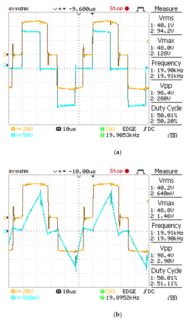
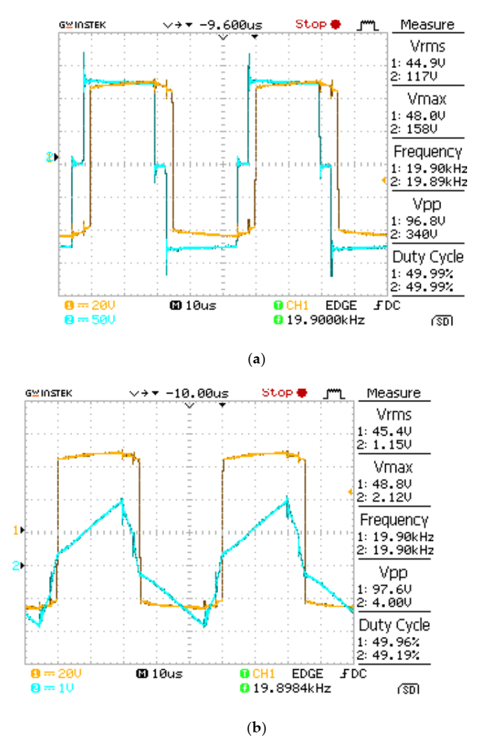
6. Experimental Results

An experimental prototype of the SAB converter has been arranged according to the findings of Section 5. Experimental voltage and current waveforms in the CCM and DCM modes are shown in Figure 15 and Figure 16, respectively. Since only a two-channel oscilloscope was available in the laboratory, two Figures are captured for each conduction mode and, to make the waveforms easy to correlate, v2 is kept common to both the plots. Waveforms in Figure 15 correspond to the converter nominal operating point, and can be compared with the theoretical ones shown in Figure 4a. Since in this Figure, point β is close to π, it is very difficult to appreciate the four different slopes for the current in each half-period of 25 μs. However, a meticulous check of the relevant values obtained from Figure 15 reveals that the theoretical analysis and the experimental outcomes are in good agreement. The waveforms of Figure 16, instead, match very well with the waveforms drawn in Figure 4c. They are obtained starting from the nominal condition, reducing β and at the same time increasing the load resistance in order to maintain a constant output voltage equal to 48 V.
The different characteristic plots of the SAB converter presented in Section 4 are compared here with the experimental results and the outcome is shown in Figure 17. The Figure shows that the star points obtained from measurements in the prototype are very close to the curves that arise from the theoretical analysis. To understand the steps to be followed to obtain the experimental measurements, let us take the case of Figure 17a which plots Po,pu as a function of β for various Vo,pu. The steps are outlined as follows: (i) the prototype is operated for a particular angle β, (ii) the load resistor is varied to attain the desired load voltage, for instance Vo = 33.6 V, which corresponds for the Vo,pu = 0.7, (iii) once the desired Vo is achieved at any load resistance Rl, Po is calculated using P o = V o 2 / R l , (iii) steps (i) to (iii) are repeated for other values of β. A similar approach is also used to obtain the results for Figure 17b–d.

7. Discussion and Conclusions

7.1. Discussion

The preceding analysis has discussed the behavior of this converter. However, the important observations can be highlighted as follows:
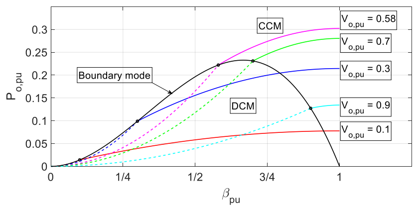
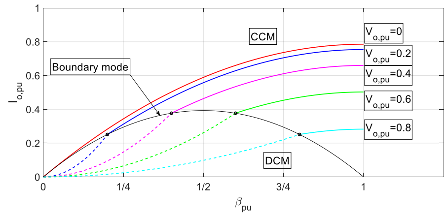
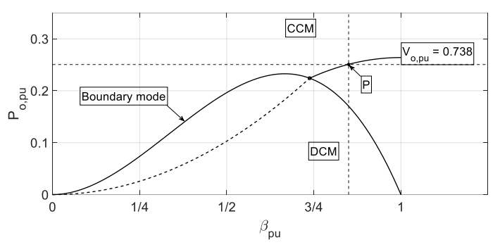
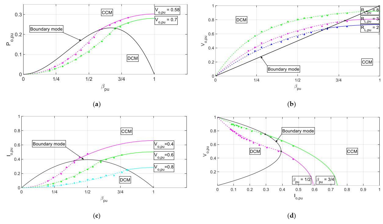
  • The output power depends not only on the phase-shift angle but also on the load voltage. The highest power that can be drawn from this converter is obtained when the phase-shift angle becomes equal to π and the load voltage is maintained at 0.58 Vnom, where the converter operates in CCM mode (see Figure 6).
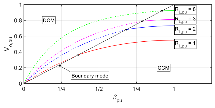
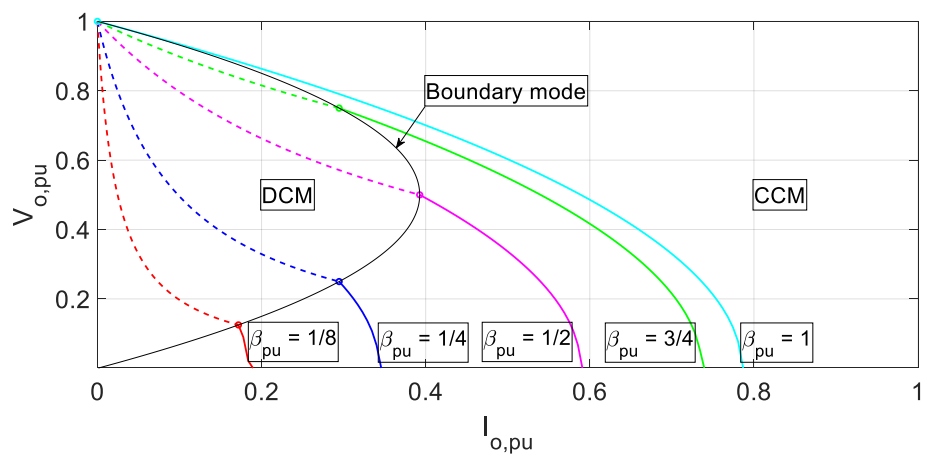
  • Load voltage increases with the phase shift angle for any value of RL and the region of DCM increases with the increase in RL value (see Figure 7).
  • The load current as a function of alpha increases monotonically and is at its maximum when Vo = 0 V i.e., when the load does not draw any current from the converter (see Figure 8).
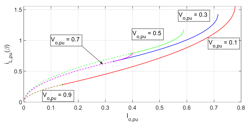
  • When the Vo is zero, i.e., output is shorted, the load current is finite and is given as Equation (27). Again when Io = 0 i.e., output is open circuit, circuit output voltage is Vo,nom. This confirms the suitability of this converter in adverse operating conditions (see Figure 9).
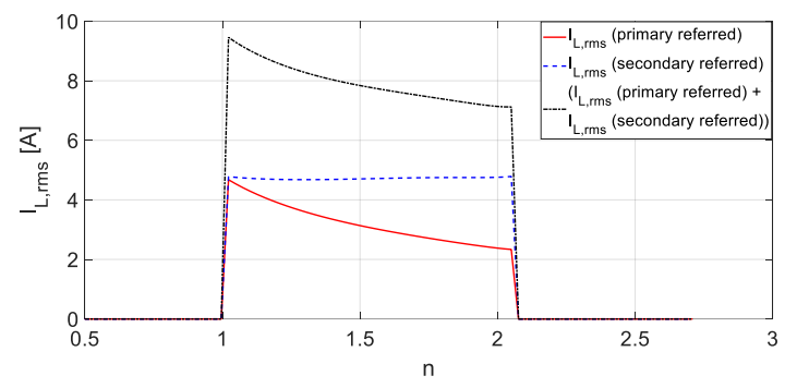
  • The transformer turns ratio can be utilized to reduce the inductor current, which, consequently, will improve efficiency. However, it should be noted that the ability of the converter to provide the nominal load current is not possible for all values of the turns ratio (see Figure 12).

7.2. Limitations, Future Scope, and Applications

7.2.1. Limitations: Limitations of this Converter Are Outlined as Follows

  • This converter suffers from large switching losses. In CCM, ZVS occurs during the turning on of the active bridge switch thus enabling soft switching, whereas turning off is hard switching. In DCM, ZCS occurs during the turn-off of the switch, whereas ZVS during switch turn-on is lost [11].
  • When the transformer ratio is equal to unity and the voltage conversion ratio is kept at unity, the power transfer is not possible because the passive bridge diode remains reverse biased. When the voltage conversion ratio is kept below unity, the total power factor of the high-frequency transformer is low [38].
  • Since primary voltage and the peak current are high in this converter, the high-voltage and high-current switching devices and the high-voltage transformer are then required.

7.2.2. Future Scope

As mentioned earlier, the converter suffers from large switching losses, which could be important to the scope of the research. The authors are also planning to continue the work on the soft switching of this converter. Another scope of the research could be the dynamic modeling of the converter [4,5,6].

7.2.3. Application

Application of this converter is generally in the area of EV charging and wind farms, where unidirectional power transfer is required.

7.3. Conclusions

The paper has presented the analysis and the step-by-step design of the SAB converter. The basic principle of the SAB converter has been reviewed, and the procedure followed in designing the converter has been thoroughly described. A systematic analysis of the converter’s characteristics has also been carried out. Afterward, a prototypal SAB converter has been set up according to the design results and tested in different operation modes. Several measurements obtained from the prototype have been reported that fully confirm the soundness of both the design procedure and the characteristics of the SAB converter.

Author Contributions

Conceptualization, R.J. and M.F.; methodology, R.J.; software, R.J. and M.F.; validation, R.J., S.P. and H.D.; formal analysis, H.D.; investigation, R.J.; resources, S.P.; writing—original draft preparation, R.J.; writing—review and editing, G.B. and M.F; supervision, R.J. All authors have read and agreed to the published version of the manuscript.

Funding

This research received no external funding.

Conflicts of Interest

The authors declare no conflict of interest.

References

  1. Inoue, S.; Akagi, H. A Bidirectional DC–DC Converter for an Energy Storage System with Galvanic Isolation. IEEE Trans. Power Electron. 2007, 22, 2299–2306. [Google Scholar] [CrossRef]
  2. Zhang, Q.; Zhao, J.; Wang, X.; Tong, L.; Jiang, H.; Zhou, J. Distribution Network Hierarchically Partitioned Optimization Considering Electric Vehicle Orderly Charging with Isolated Bidirectional DC-DC Converter Optimal Efficiency Model. Energies 2021, 14, 1614. [Google Scholar] [CrossRef]
  3. Ojeda-Rodríguez, Á.; González-Vizuete, P.; Bernal-Méndez, J.; Martín-Prats, M.A. A Survey on Bidirectional DC/DC Power Converter Topologies for the Future Hybrid and All Electric Aircrafts. Energies 2020, 13, 4883. [Google Scholar] [CrossRef]
  4. Iqbal, M.T.; Maswood, A.I. An Explicit Discrete-Time Large- and Small-Signal Modeling of the Dual Active Bridge DC–DC Converter Based on the Time Scale Methodology. IEEE J. Emerg. Sel. Top. Ind. Electron. 2021, 2, 545–555. [Google Scholar] [CrossRef]
  5. Iqbal, M.T.; Maswood, A.I.; Yeo, K.; Tariq, M. Dynamic Model and Analysis of Three phase YD Transformer Based Dual Active Bridge Using Optimised Harmonic Number for Solid State Transformer in Distributed System. In Proceedings of the 2018 IEEE Innovative Smart Grid Technologies—Asia (ISGT Asia), Singapore, 22–25 May 2018; IEEE: New York, NY, USA, 2018; pp. 523–527. [Google Scholar]
  6. Iqbal, M.T.; Maswood, A.I. A frequency domain based large and small signal modeling of three phase dual active bridge. In Proceedings of the IECON 2020 The 46th Annual Conference of the IEEE Industrial Electronics Society, Singapore, 9 December 2020; IEEE: New York, NY, USA, 2020; pp. 3421–3426. [Google Scholar]
  7. Ríos, S.J.; Pagano, D.J.; Lucas, K.E. Bidirectional Power Sharing for DC Microgrid Enabled by Dual Active Bridge DC-DC Converter. Energies 2021, 14, 404. [Google Scholar] [CrossRef]
  8. Rodríguez, A.; Vázquez, A.; Lamar, D.G.; Sebastián, M.M.H.J. Different Purpose Design Strategies and Techniques to Improve the Performance of a Dual Active Bridge with Phase-Shift Control. IEEE Trans. Power Electron. 2015, 30, 790–804. [Google Scholar] [CrossRef]
  9. Henao-Bravo, E.E.; Ramos-Paja, C.A.; Saavedra-Montes, A.J.; González-Montoya, D.; Sierra-Pérez, J. Design Method of Dual Active Bridge Converters for Photovoltaic Systems with High Voltage Gain. Energies 2020, 13, 1711. [Google Scholar] [CrossRef] [Green Version]
  10. Demetriades, G.D.; Nee, H.P. Characterisation of the Soft-switched Single-Active Bridge Topology Employing a Novel Control Scheme for High-power DC-DC Applications. In Proceedings of the 2005 IEEE 36th Power Electronics Specialists Conference, Dresden, Germany, 16 June 2005; pp. 1947–1951. [Google Scholar] [CrossRef]
  11. Ting, Y.; De Haan, S.; Ferreira, J.A. Elimination of switching losses in the single active bridge over a wide voltage and load range at constant frequency. In Proceedings of the 2013 15th European Conference on Power Electronics and Applications (EPE), Lille, France, 2–6 September 2013; pp. 1–10. [Google Scholar]
  12. Sha, D.; Zhang, J.; Sun, T. Multimode Control Strategy for SiC mosfets Based Semi-Dual Active Bridge DC–DC Converter. IEEE Trans. Power Electron. 2018, 34, 5476–5486. [Google Scholar] [CrossRef]
  13. Kulasekaran, S.; Ayyanar, R. Analysis, Design, and Experimental Results of the Semidual-Active-Bridge Converter. IEEE Trans. Power Electron. 2014, 29, 5136–5147. [Google Scholar] [CrossRef]
  14. Yadav, G.N.B.; Narasamma, N.L. An Active Soft Switched Phase-Shifted Full-Bridge DC–DC Converter: Analysis, Modeling, Design, and Implementation. IEEE Trans. Power Electron. 2014, 29, 4538–4550. [Google Scholar] [CrossRef]
  15. Wolski, K.; Grzejszczak, P.; Szymczak, M.; Barlik, R. Closed-Form Formulas for Automated Design of SiC-Based Phase-Shifted Full Bridge Converters in Charger Applications. Energies 2021, 14, 5380. [Google Scholar] [CrossRef]
  16. Escudero, M.; Meneses, D.; Rodriguez, N.; Morales, D.P. Modulation Scheme for the Bidirectional Operation of the Phase-Shift Full-Bridge Power Converter. IEEE Trans. Power Electron. 2019, 35, 1377–1391. [Google Scholar] [CrossRef]
  17. Li, G.; Xia, J.; Wang, K.; Deng, Y.; He, X.; Wang, Y. Hybrid Modulation of Parallel-Series LLCLLC. Resonant Converter and Phase Shift Full-Bridge Converter for a Dual-Output DC–DC Converter. IEEE J. Emerg. Sel. Top. Power Electron. 2019, 7, 833–842. [Google Scholar] [CrossRef]
  18. Jung, J.H.; Kim, H.S.; Ryu, M.H.; Baek, J.W. Design Methodology of Bidirectional CLLC Resonant Converter for High-Frequency Isolation of DC Distribution Systems. IEEE Trans. Power Electron. 2013, 28, 1741–1755. [Google Scholar] [CrossRef]
  19. Chen, W.; Rong, P.; Lu, Z. Snubberless Bidirectional DC–DC Converter with New CLLC Resonant Tank Featuring Minimized Switching Loss. IEEE Trans. Ind. Electron. 2010, 57, 3075–3086. [Google Scholar] [CrossRef]
  20. Bakeer, A.; Chub, A.; Blinov, A.; Lai, J.-S. Wide Range Series Resonant DC-DC Converter with a Reduced Component Count and Capacitor Voltage Stress for Distributed Generation. Energies 2021, 14, 2051. [Google Scholar] [CrossRef]
  21. Li, X.; Bhat, A.K.S. Analysis and Design of High-Frequency Isolated Dual-Bridge Series Resonant DC/DC Converter. IEEE Trans. Power Electron. 2010, 25, 850–862. [Google Scholar] [CrossRef]
  22. Tuan, C.A.; Takeshita, T. Analysis of Unidirectional Secondary Resonant Single Active Bridge DC–DC Converter. Energies 2021, 14, 6349. [Google Scholar] [CrossRef]
  23. Mweene, L.H.; Wright, C.A.; Schlecht, M.F. A 1 kW 500 kHz Front-End Converter for A Distributed Power Supply System. IEEE Trans. Power Electron. 1991, 6, 398–407. [Google Scholar] [CrossRef]
  24. Singh, S.A.; Ronanki, D.; Praneeth, A.V.J.S.; Williamson, S. State-of-the-art Charging Solutions for Electric Transportation and Autonomous E-mobility. J. Renew. Energy Sustain. Dev. 2018, 4, 2–13. [Google Scholar] [CrossRef]
  25. Park, K.; Chen, Z. Analysis and design of a parallel-connected single active bridge DC-DC converter for high-power wind farm applications. In Proceedings of the 2013 15th European Conference on Power Electronics and Applications (EPE), Lille, France, 13 October 2013; pp. 1–10. [Google Scholar]
  26. Ting, Y.; de Haan, S.; Ferreira, J.A. Efficiency improvements in a Single Active Bridge modular DC-DC converter with snubber capacitance optimization. In Proceedings of the IEEE International Power Electronics Conference (IPEC-Hiroshima 2014—ECCE ASIA), Hiroshima, Japan, 17 August 2014; pp. 2787–2793. [Google Scholar]
  27. Ting, Y.; De Haan, S.; Ferreira, J.A. The partial-resonant single active bridge DC-DC converter for conduction losses reduction in the single active bridge. In Proceedings of the 2013 IEEE ECCE Asia Downunder, Melbourne, VIC, Australia, 3–6 June 2013; pp. 987–993. [Google Scholar]
  28. Park, K.; Chen, Z. Open-circuit fault detection and tolerant operation for a parallel-connected SAB DC-DC converter. In Proceedings of the 2014 IEEE Applied Power Electronics Conference and Exposition—APEC, Fort Worth, TX, USA, 16–20 March 2014; pp. 1966–1972. [Google Scholar]
  29. Averberg, A.; Mertens, A. Characteristics of the single active bridge converter with voltage doubler. In Proceedings of the 2008 13th International Power Electronics and Motion Control Conference, Poznan, Poland, 1–3 September 2008; pp. 213–220. [Google Scholar]
  30. Fontana, C.; Forato, M.; Bertoluzzo, M.; Buja, G. Design characteristics of SAB and DAB converters. In Proceedings of the 2015 Intl Aegean Conference on Electrical Machines & Power Electronics (ACEMP), 2015 Intl Conference on Optimization of Electrical & Electronic Equipment (OPTIM) & 2015 Intl Symposium on Advanced Electromechanical Motion Systems (ELECTROMOTION), Side, Turkey, 21 August 2015; pp. 661–668. [Google Scholar]
  31. Fontana, C.; Forato, M.; Kumar, K.; Outeiro, M.T.; Bertoluzzo, M.; Buja, G. Soft-switching capabilities of SAB vs. DAB converters. In Proceedings of the IECON 2015—41st Annual Conference of the IEEE Industrial Electronics Society, Yokohama, Japan, 9–12 November 2015; pp. 003485–003490. [Google Scholar]
  32. Tan, N.M.L.; Abe, T.; Akagi, H. Design and Performance of a Bidirectional Isolated DC–DC Converter for a Battery Energy Storage System. IEEE Trans. Power Electron. 2012, 27, 1237–1248. [Google Scholar] [CrossRef]
  33. Sang, Y.; Ferre, A.J.; Green, T.C. Operational Principles of Three-Phase Single Active Bridge DC/DC Converters Under Duty Cycle Control. IEEE Trans. Power Electron. 2020, 35, 8737–8750. [Google Scholar] [CrossRef]
  34. Mi, C.; Bai, H.; Wang, C.; Gargies, S. Operation, design and control of dual H-bridge-based isolated bidirectional DC–DC converter. IET Power Electron. 2008, 1, 507–517. [Google Scholar] [CrossRef] [Green Version]
  35. Nguyen, D.-D.; Bui, N.-T.; Yukita, K. Design and Optimization of Three-Phase Dual-Active-Bridge Converters for Electric Vehicle Charging Stations. Energies 2019, 13, 150. [Google Scholar] [CrossRef] [Green Version]
  36. Escudero, M.; Kutschak, M.-A.; Meneses, D.; Rodriguez, N.; Morales, D.P. A Practical Approach to the Design of a Highly Efficient PSFB DC-DC Converter for Server Applications. Energies 2019, 12, 3723. [Google Scholar] [CrossRef] [Green Version]
  37. Erickson, R.W.; Maksimovic, D. Fundamentals of Power Electronics; Kluwer: Norwell, MA, USA, 2001. [Google Scholar]
  38. Doncker, R.W.D.; Divan, D.M.; Kheraluwala, M.H. A Three Phase Soft–Switched High–Power–Density DC/DC Converter for High–Power Applications. IEEE Trans. Ind Elect. 1991, 27, 63–73. [Google Scholar] [CrossRef]
Figure 1. General schematic of an isolated dc-dc converter.
Energies 15 00666 g001
Figure 2. Methodology used for the article.
Energies 15 00666 g002
Figure 3. Circuit diagram of a SAB converter.
Energies 15 00666 g003
Figure 4. Voltages and currents waveforms of the SAB converter operating in (a) CCM (b) BCM (c) DCM.
Energies 15 00666 g004
Figure 5. Currents paths and devices conduction of the SAB converter during (a) interval 1 [0 ÷ φ], (b) interval 2 [φ ÷ β] (c) interval 3 [β ÷ π].
Energies 15 00666 g005
Figure 6. SAB converter output power vs. the phase-shift angle for different values of the output voltage. Continuous curves refer to CCM whereas the dashed ones refer to DCM.
Energies 15 00666 g006
Figure 7. SAB converter output voltage vs. the phase-shift angle for different values of load resistance. Continuous curves refer to CCM, whereas the dashed ones refer to DCM.
Energies 15 00666 g007
Figure 8. SAB converter output current vs. the phase-shift angle for different values of the output voltage. Continuous curves refer to CCM whereas the dashed ones refer to DCM.
Energies 15 00666 g008
Figure 9. External characteristic of the SAB converter. Continuous curves refer to CCM whereas the dashed ones refer to DCM.
Energies 15 00666 g009
Figure 10. Value of iL,pu(β) as a function of the average current delivered by the SAB converter for different values of the output voltage. Continuous curves refer to CCM, whereas the dashed ones refer to DCM.
Energies 15 00666 g010
Figure 11. Waveform of the current iout; colored areas represent the charge ∆Q.
Energies 15 00666 g011
Figure 12. Plot of IL,rms (primary and secondary referred) vs. transformer turn ratio n for L equal to 168 µH. The sum of the two currents is also shown.
Energies 15 00666 g012
Figure 13. Nominal working point of the prototypal SAB converter.
Energies 15 00666 g013
Figure 14. Flow chart for SAB elements design.
Energies 15 00666 g014
Figure 15. Experimental waveforms for SAB in CCM mode; (a) v2 (channel 1) and v1 (channel 2). (b) v2 (channel 1) and iL (channel 2, 1 V correspond to 2 A).
Energies 15 00666 g015
Figure 16. Experimental waveforms for SAB in DCM mode; (a) v2 (channel 1) and v1 (channel 2). (b) v2 (channel 1) and iL (channel 2, 1 V correspond to 2 A).
Energies 15 00666 g016
Figure 17. Validation of theoretical findings: (a) Po,pu vs. βpu, (b) Vo,pu vs. βpu, (c) Io,pu vs. βpu, (d) Vo.pu vs. βpu. The continuous curves refer to CCM, the dashed ones refer to DCM and the stars represent experimental results.
Energies 15 00666 g017
Table 2. rms Values of Currents.
CCMDCM
I Q 1 ,   r m s 1 6 π i L 2 β π φ + i L 2 0 π β + i L β i L 0 β π   29 1 6 π i L 2 β π α   34
I D 1 ,   r m s 1 6 π i L 2 0   φ   30 0 (35)
I Q 3 ,   r m s 1 6 π i L 2 β β φ   31 1 6 π i L 2 β   β   36
I D 3 ,   r m s 1 6 π i L 2 β π β + i L 2 0 π β + φ + i L β i L 0 β π 32 1 6 π i L 2 β π α β 37
I o u t , r m s 1 3 π i L 2 β π φ + i L 2 0 π β + φ + i L β i L 0 β π   33 1 3 π i L 2 β π α   38
Table 3. SAB Converter Specifications.
ParameterSymbolNominal Data
Input voltageVi130 V
Output voltageVo48 V
Output powerPo200 W
Switching Frequencyfs20 kHz
Publisher’s Note: MDPI stays neutral with regard to jurisdictional claims in published maps and institutional affiliations.

