1. Introduction
As we all know, in today’s world, under the double challenges of global fossil energy depletion and environmental pollution, the most promising access for eliminating these shortcomings is to replace fossil fuel cars with new energy electric vehicles (NEEVs). There are many incentives to support the use of NEEVs because the technology is environmentally friendly and has zero emissions compared to internal combustion engine technology [
1,
2,
3,
4]. For decades, consumers, manufacturers, and inventors have been thinking about the idea of electrification of transportation, which requires the development of NEEVs, a promising way to green the transportation system and reduce the problems of climate change [
5,
6,
7,
8].
Generally, in [
9,
10,
11], the NEEVs can be divided into the following types according to the power source: battery electric vehicles (BEVs), hybrid electric vehicles (HEVs), photovoltaic electric vehicles (PEVs), fuel cell electric vehicles (FCEVs) and plug-in hybrid electric vehicles (PHEVs).
When the NEEVs are running normally, the bidirectional DC/DC (Bi-DC/DC) converter plays an important role as the core factor of electrical energy flow regulation and management between the battery pack and motor drive inverter within the high voltage direct current bus, and transform voltage from two conversion directions, so that the motor drive system is always working in the optimal rate zone [
12,
13]. In the process of starting or accelerating, the electrical energy flows forward to ensure the motor inverter drive performance; during braking or decelerating, the electrical energy flows back to effectively recover the excess electrical energy. The performance of the Bi-DC/DC converter determines the power output and cruising range of the NEEVs, which directly has a deep impact on the performance, quality, and user experience [
14,
15,
16].
The NEEVs adopt a Bi-DC/DC converter, which can reduce the power battery pack voltage level, improve the safety of the whole EVs, and cut costs of the battery management system (BMS); the voltage decoupling of the battery pack can input and output the most suitable and stable electrical energy according to the drive motor operating conditions, which is conducive to decrease the volume and weight of the drive motor; in addition, when the drive motor fails, the Bi-DC/DC converter can also effectively block high voltage that may be generated from the direct current bus at the end of three-phase inverter bridge, so as not to be directly introduced into the battery pack to cause potential risks, thereby improving the safety and reliability of the system.
Among the traditional Bi-DC/DC converter, the bidirectional buck–boost (bi-buck–boost) converter is the most widely used in NEEVs. To solve the problems, several new circuit topologies and control strategies have been introduced to improve the performance of the buck–boost converters for NEEVs, some excellent research papers on this topic have been conducted as shown in [
17,
18,
19,
20,
21,
22,
23]. In [
17], the working of buck–boost converter as a power factor correction controller applicable for battery charging in electric vehicles application, also satisfies the harmonic compliance of source current in accordance with the IEEE519 recommendations. A charger of a three-port structure [
18] is realized with level-3 charging capability using a current source converter frontend together with an input filter, a polarity inversion module, and a differentially connected dual inverter drive. Additionally, due to the limited range of a single charge, the charging NEEVS is one major barrier. Thus, this paper [
19] analyzed a dual input buck–boost converter (DIBBC) and proposed charging of battery pack by solar PV and DynamicWPT. In [
20], a bidirectional multi-level diode-clamped buck–boost converter is proposed, and GaN HEMT switching devices are used to deal with both concerns about low efficiency and power density in the NEEVs application. A series of integrated equalizers based on joint buck–boost and switched-capacitor converters are proposed in [
21] for balancing the voltages of series-connected battery packs. All these equalizers realize the any-cells-to-any-cells (AC2AC) equalization mode without increasing the count of MOSFETs and drivers. The work [
22] explores the use of dual-carrier switching modulation schemes for the bidirectional buck–boost converters. The buck–boost scheme is utilized as the power converter topology to interface a storage system to a DC-link in electrical vehicles (EVs) and hybrid electric vehicles (HEVs). This paper [
23] proposes an input-parallel output-series (IPOS) connected bidirectional buck–boost converter is introduced that can dynamically vary the DC-link voltage of an electric vehicle power train.
From the above literature review, it can be found that the interleaved parallel multiphase identical circuits technology is widely used in low voltage and high current with large power supply occasions, which has more significant advantages than single-phase circuit [
24,
25]:
Each phase circuit only shares part of the power capacity, reducing the voltage and current stress of electronic switch devices.
Improve reliability, even if there are problems in one phase circuit, other phase circuits can still work normally.
High-efficiency range of the circuit can be widened by switching phase mode under different power levels.
Interleaved parallel technology can improve the equivalent switching frequency of the whole system, depress current ripple, and help to reduce the volume and weight of the filter.
In large power applications of the NEEVs, the requirements for power switching devices, rectifier diodes, filter capacitors, energy storage inductors, and other parts (active and passive) are becoming much higher than before, which leads to difficulties in circuit design. Therefore, in order to effectively increase power and reduce voltage and current stress of electronic components, improve the inherent high ripple rate disadvantage of the traditional bi-buck–boost converter, a three-phase interleaved parallel bidirectional buck–boost (TPIPBi-Buck–Boost) converter is analyzed, and designed in this paper, study circuit topology and control strategy, which has very important theoretical research value and broad practical application prospects. In recent years, it is also the hot spot of the energy management system in NEEVs.
The rest of this paper is structured into six sections,
Section 2 describes circuit topology, operation states, and equivalent circuit expressions of the TPIPBi-Buck–Boost converter are derived. Thereafter in
Section 3, the mathematical model based on AC small signal is obtained. In
Section 4, the digital implementation is used by XDPTM Digital Power Controllers XDPP1100-Q040 of Infineon Technologies AG. subsequently, the experimental results are demonstrated in
Section 5. Finally, brief conclusions, contributions, and potential applications are summarized accordingly in
Section 6.
2. Principal Configuration and Operation State in TPIPBi-Buck–Boost Converter
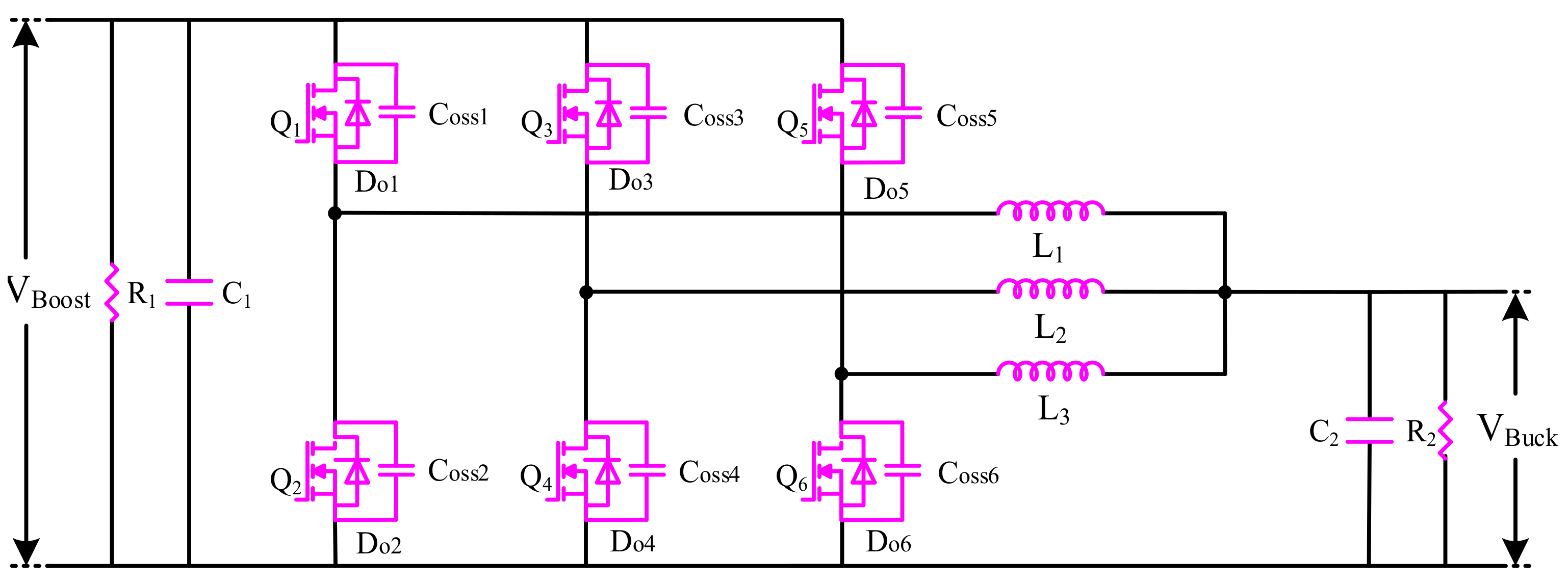
As shown in
Figure 1, the TPIPBi-buck–boost converter, which integrates three same topological structures,
is the high-voltage side of the direct current bus,
is the low-voltage side of the power battery pack,
to
are the SiC MOSFETs while
to
and
to
are their parasitic anti-parallel diodes and block capacitors,
to
is the energy storage inductors,
to
and
to
are the load resistors and filter capacitors of input and output, respectively.
,
,
,
,
, and
are connected in series on three-phase inverter bridge, the upper and lower power switches adopt pulse width modulation (PWM) phase shift interleaved complementary control method, and the phase angle of the drive signal differs by 2
π/3 = 120° in turn (regardless of dead time).
Based on the above analysis, the TPIPBi-Buck–Boost converter has three operating modes:
Charge buck mode, the battery pack stores the feedback electric energy from the motor drive inverter in the direct current bus through the boost–buck converter.
Discharge boost mode, the battery pack release the inner electric energy for direct current bus through the buck–boost converter to maintain voltage stability.
Electric energy interaction mode, when the EVs run normally, transmit and exchange bidirectional electric energy in real time between the power battery pack and direct current bus, so that the buck and boost mode can always switch quickly to prevent overcharge or over-discharge of the battery pack.
In order to clarify the operation modes of the TPIPBi-Buck–Boost converter, the battery pack is equivalent to the direct current power supply, and its internal resistance and voltage equalization between single modules are ignored. Some assumptions are summarized as follows:
The electrical components and parameters of each phase circuit are the same, and the circulating current loss is not considered.
The switch drive signal of each phase shift circuit is strictly conducted, and the phase-to-phase current is equal without offset.
The converter is in a stable state, and the inductance works in continuous conduction mode (CCM), regardless of non-ideal saturation conditions.
2.1. Charge Buck Mode of TPIPBi-Buck–Boost Converter
The switching cycle of the TPIPBi-Buck–Boost converter in charge buck mode can be dived into eight stages, corresponding to the eight equivalent circuits shown in
Figure 2. The operation stages are described as follows:
Stage 1 (
Figure 2a):
,
, and
are turned off, at the same time,
,
, and
conduct naturally, while high voltage side
stores
,
and
are transmitting electrical energy to the low voltage side
. The voltage drops of the
to
and current of the
are given as follows:
Stage 2 (
Figure 2b):
turn on,
and
are turned off, at the same time,
and
conduct naturally,
is off, while high voltage side
stores
together with
and
are transmitting electrical energy to the low voltage side
. The voltage drops of the
to
and current of the
are given as follows:
Stage 3 (
Figure 2c):
turn on,
and
are turned off, at the same time,
and
conduct naturally,
is off, while high voltage side
stores
together with
and
are transmitting electrical energy to the low voltage side
. The voltage drops of the
to
and current of the
are given as follows:
Stage 4 (
Figure 2d):
turn on,
and
are turned off, at the same time,
and
conduct naturally,
is off, while high voltage side
stores
together with
and
are transmitting electrical energy to the low voltage side
. The voltage drops of the
to
and current of the
are given as follows:
Stage 5 (
Figure 2e):
and
turn on,
is turned off, at the same time,
conducts naturally,
and
are off, while high voltage side
stores
and
together with
are transmitting electrical energy to the low voltage side
. The voltage drops of the
to
and current of the
are given as follows:
Stage 6 (
Figure 2f):
and
turn on,
is turned off, at the same time,
conducts naturally,
and
are off, while high voltage side
stores
and
together with
are transmitting electrical energy to the low voltage side
. The voltage drops of the
to
and current of the
are given as follows:
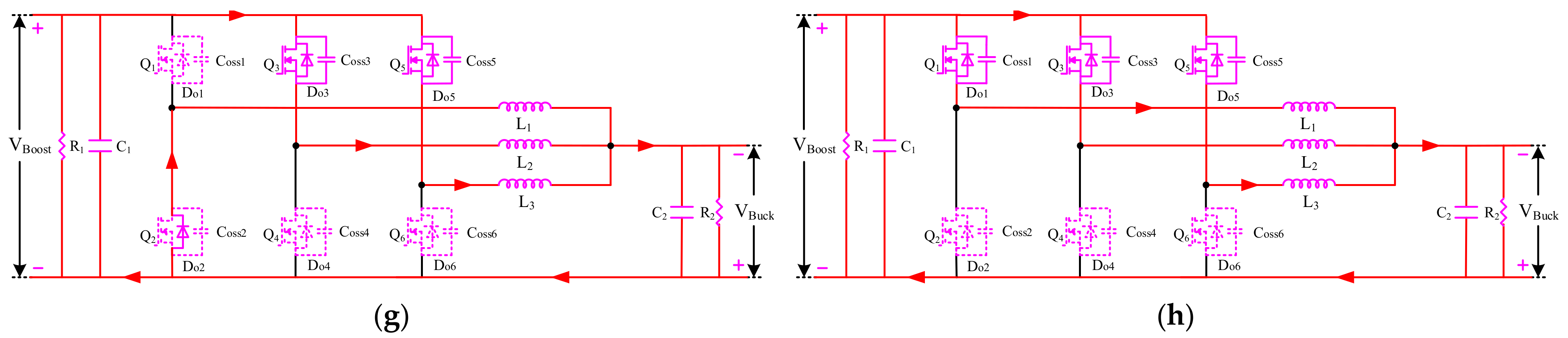
Stage 7 (
Figure 2g):
and
turn on,
is turned off, at the same time,
conducts naturally,
and
are off, while high voltage side
stores
and
together with
are transmitting electrical energy to the low voltage side
. The voltage drops of the
to
and current of the
are given as follows:
Stage 8 (
Figure 2h):
,
and
turn on, at the same time,
,
and
are off, while high voltage side
stores
,
and
are transmitting electrical energy to the low voltage side
. The voltage drops of the
to
and current of the
are given as follows:
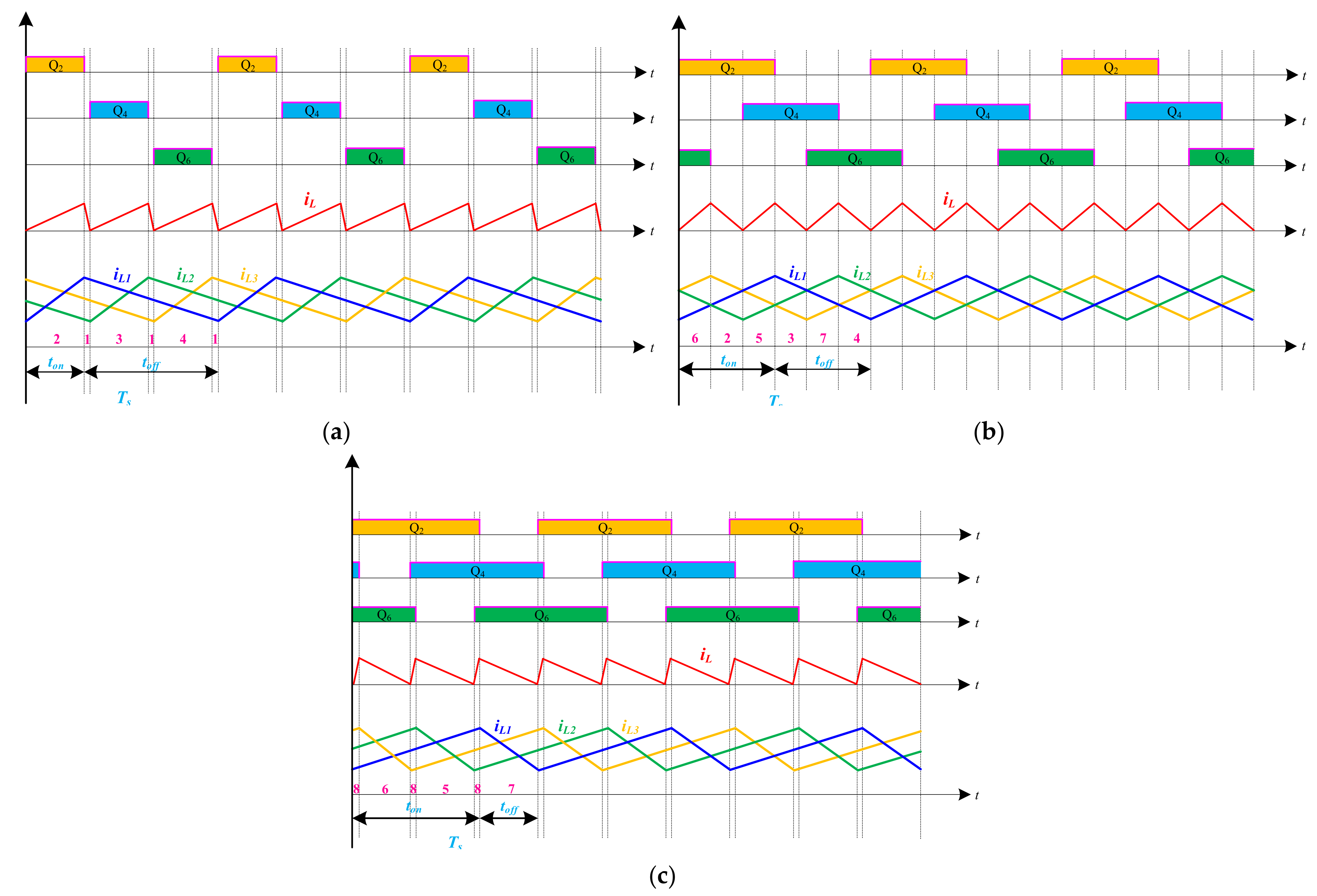
The key waveforms of the charge buck mode of TPIPBi-Buck–Boost converter are shown in
Figure 3. In each switching cycle,
Table 1 depicts that they can be divided into three cases:
2.2. Discharge Boost Mode of TPIPBi-Buck–Boost Converter
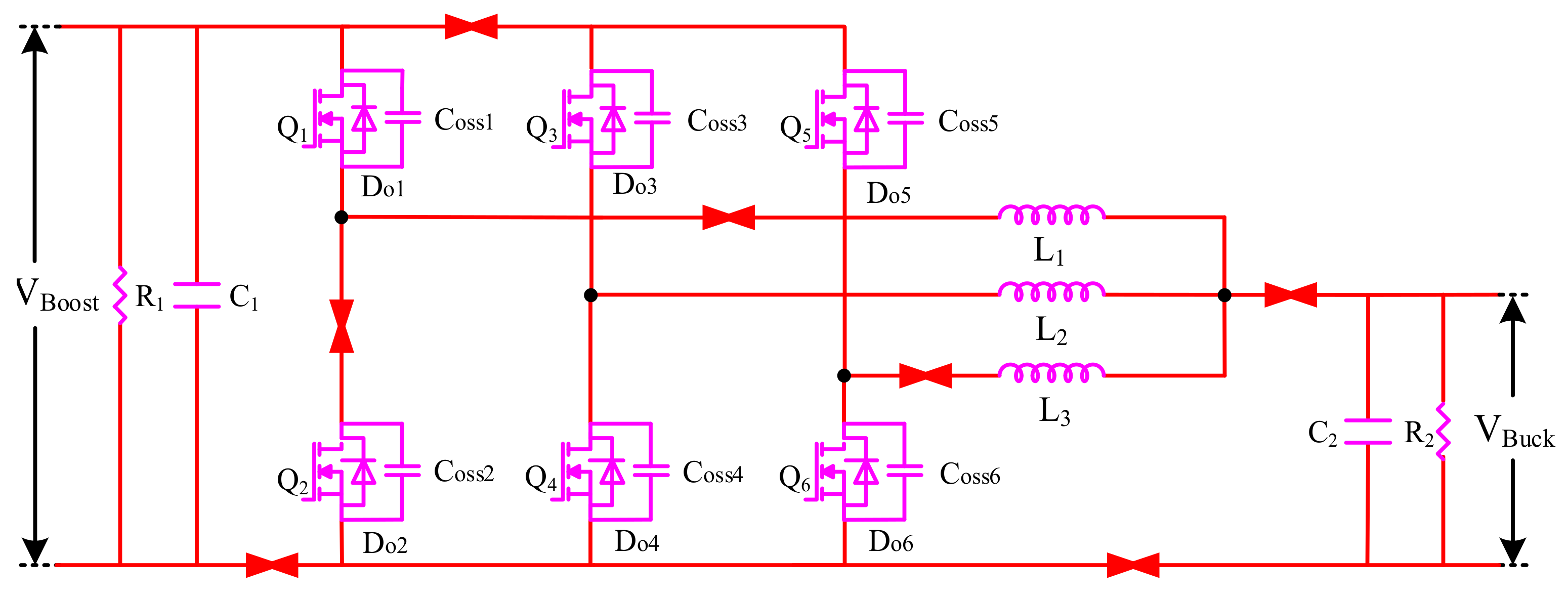
The switching cycle in discharge boost mode of the TPIPBi-Buck–Boost converter can be divided into eight stages in a similar way, corresponding to the eight equivalent circuits shown in
Figure 4. The operation stages are also described as follows:
Stage 1 (
Figure 4a):
,
and
are turned off, at the same time,
,
and
conduct naturally, while low voltage side
stores
,
and
are transmitting electrical energy to the high voltage side
. The voltage drops of the
to
and current of the
are given as follows:
Stage 2 (
Figure 4b):
turn on,
and
are turned off, at the same time,
and
conduct naturally,
is off, while low voltage side
stores
together with
and
are transmitting electrical energy to the high voltage side
. The voltage drops of the
to
and current of the
are given as follows:
Stage 3 (
Figure 4c):
turn on,
and
are turned off, at the same time,
and
conduct naturally,
is off, while low voltage side
stores
together with
and
are transmitting electrical energy to the high voltage side
. The voltage drops of the
to
and current of the
are given as follows:
Stage 4 (
Figure 4d):
turn on,
and
are turned off, at the same time,
and
conduct naturally,
is off, while low voltage side
stores
together with
and
are transmitting electrical energy to the high voltage side
. The voltage drops of the
to
and current of the
are given as follows:
Stage 5 (
Figure 4e):
and
turn on,
is turned off, at the same time,
conducts naturally,
and
are off, while low voltage side
stores
and
together with
are transmitting electrical energy to the high voltage side
. The voltage drops of the
to
and current of the
are given as follows:
Stage 6 (
Figure 4f):
and
turn on,
is turned off, at the same time,
conducts naturally,
and
are off, while low voltage side
stores
and
together with
are transmitting electrical energy to the high voltage side
. The voltage drops of the
to
and current of the
are given as follows:
Stage 7 (
Figure 4g):
and
turn on,
is turned off, at the same time,
conducts naturally,
and
are off, while low voltage side
stores
and
together with
are transmitting electrical energy to the high voltage side
. The voltage drops of the
to
and current of the
are given as follows:
Stage 8 (
Figure 4h):
,
and
turn on, at the same time,
,
and
are off, while low voltage side
stores
,
and
are transmitting electrical energy to the high voltage side
. The voltage drops of the
to
and current of the
are given as follows:
The key waveforms of the charge buck mode of TPIPBi-Buck–Boost converter are shown in
Figure 5. In each switching cycle,
Table 2 depicts that they can be divided into three cases:
2.3. Electrical Energy Interaction Mode
The previous theoretical analysis proves that the TPIPBi-Buck–Boost converter not only achieves charge buck and discharge boost mode, but also has the ability of real-time bidirectional electrical energy exchange when the entire system is working properly.
As shown in
Figure 6, in the electrical energy interaction mode, when the EVs run normally, the battery pack and direct current bus transmit real-time bidirectional electrical energy exchange, so that the TPIPBi-Buck–Boost converter can switch between charge buck mode and discharge boost mode quickly, smoothly and flexibly, to prevent overcharge or overdischarge of the battery pack. In addition, this electrical energy interaction mode is not fundamentally different from the working conditions of Buck and Boost conversion of normal circuits. The drive angle of the power switches
to
are phase-shifted by 120° and independent of each other, which avoids the discontinuous current conduction of the energy storage inductors
to
when the light load, poor current stability, and large instantaneous inrush current when the modes are switching. In this mode, regardless of whether charge buck mode and discharge boost mode is implemented, the duty cycle of
,
,
, or
,
,
are correspondingly close to 0. Both the low voltage side
and high voltage side
of the TPIPBi-Buck–Boost converter is kept constant and energy exchange is realized, to hold the voltage stability of the battery pack and the direct current bus in all circumstances.
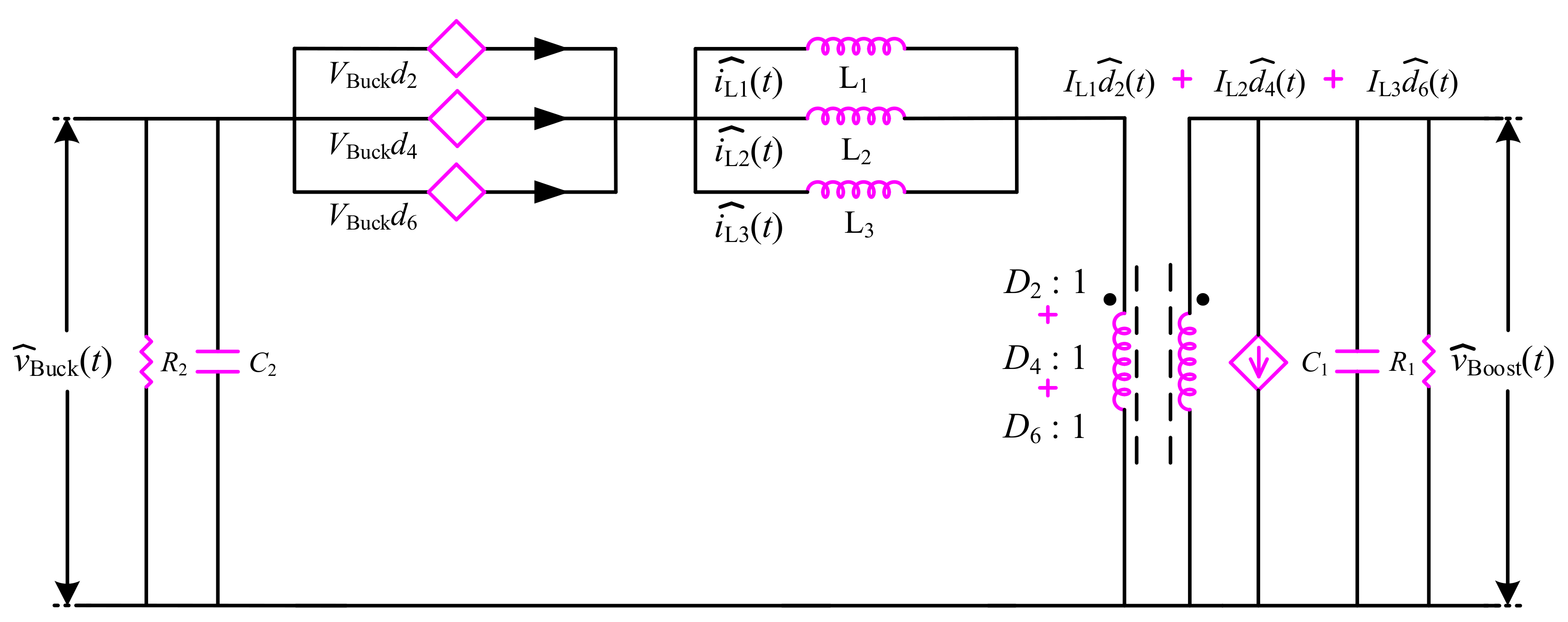
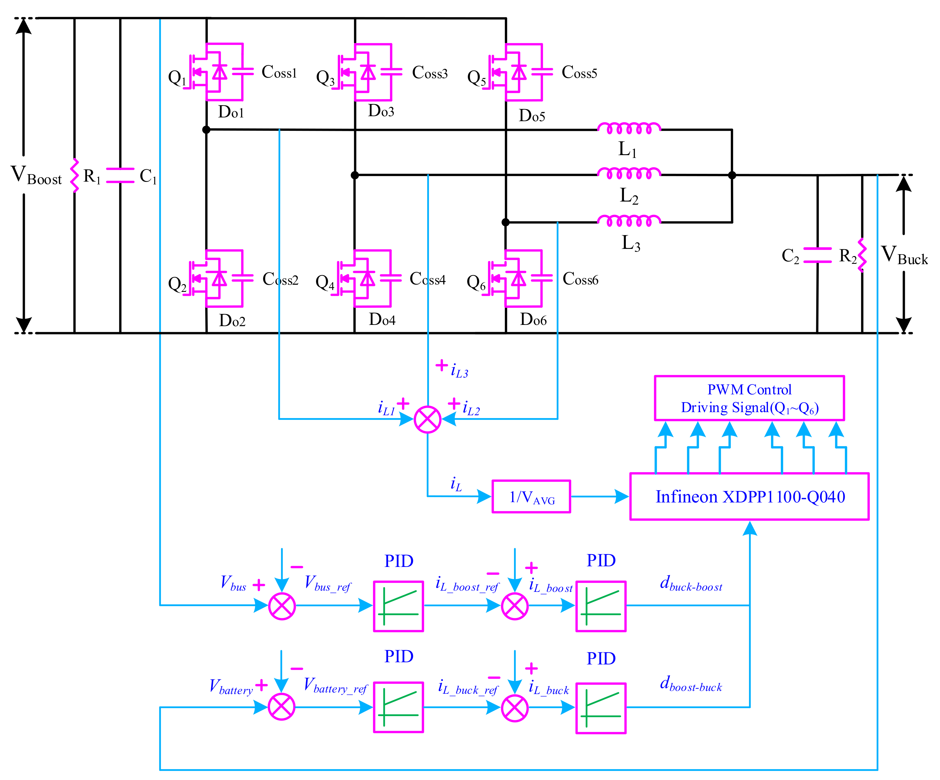
4. Digital Implementation for TPIPBi-Buck–Boost Converter with Infineon
The analysis and design of the control method determine the performance of the TPIPBi-Buck–Boost converter, which is the focus and difficulty of the whole system. In order to improve the stability and dynamic response of the new energy electric vehicles (NEEVs),
Section 4 will combine the open loop derivation results based on the AC small signal model in
Section 3, and purposefully carry out the optimal design of the double closed-loop control system with XDP
TM Digital Power Controllers by Infineon Technologies AG, which also provides an important theoretical basis for the concrete realization methods of hardware and software [
28,
29,
30].
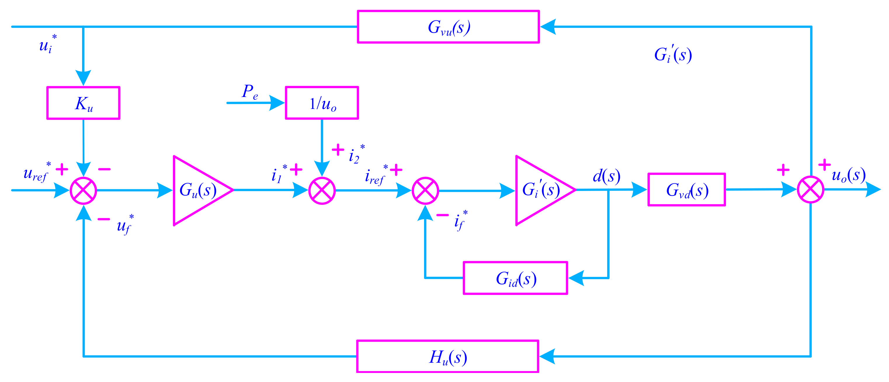
4.1. Analysis and Design of Double Closed-Loop Control System
According to the actual application requirements, in the process of frequent starting, acceleration, deceleration, and braking of the drive motor, the voltage, and current of the direct current bus are constantly changing in a wide range. For the TPIPBi-Buck–Boost converter with different power flow directions, the transfer functions are also very different, and stable and accurate control is relatively difficult.
In view of the specific requirements of the above problems, a double closed-loop control strategy is considered in
Figure 9, in which the voltage loop is used as the outer loop and the current loop as the inner loop, which not only enhances the system stability, but also improves the dynamic response. Analyzing the TPIPBi-Buck–Boost converter circuit topology, low voltage side
and high voltage side
, a novel control strategy is adopted to place the controlled voltage and current at different sides, it not only achieves that the direct current bus voltage is controlled in the forward direction, and the reverse charging current of the battery pack is well controlled.
In the digital signal control system, the direct bus voltage and the energy storage inductor current are simultaneously sampled in one sampling period, converted into digital signals by A/D, digitally filtered, and subtracted from the corresponding offset to obtain the digital signal. The high side voltage terminal command is given by the Infineon XDPP1100-Q040, and compared with the voltage sampling value to obtain the voltage error signal, the output value obtains the current given signal through the PID regulator, and the current given signal is compared with the current sampling value to obtain the current error signal, the output value of the PWM register is output through the PID regulator, so as to achieve the purpose of controlling the high side voltage output and low side current.
Where is the voltage loop correction network transfer function, is the current loop correction network transfer function, is the delay caused by digital sampling, calculation and update of the duty cycle, is the transfer function of duty cycle to the inductive current, is the transfer function of duty cycle to the input and output voltage, is the transfer function for voltage sampling.
4.2. Current Inner Loop Compensation Controller
In
Figure 10, the current inner loop is designed with a PI controller. Since the delay segment does not change the system gain, only changes the phase, and is not considered, for the time being, the open loop transfer function of the current inner loop can be expressed as
The closed-loop transfer function of the current inner loop:
where
,
,
,
,
.
From the analysis of Equation (50), it can be known that
is much smaller than the other coefficients and the
is negligible:
Therefore, in Equation (50), the current inner loop is equivalent to a proportional segment, which further verifies the correctness of the previous Bode diagram analysis conclusion. In the system, the delay segment can be equivalent to a first-order inertial segment, and the influence of the pole can be offset by the PI parameter of the current inner loop.
4.3. Voltage Outer Loop Compensation Controller
For the TPIPBi-Buck–Boost converter with insufficient phase and amplitude margins in open loop state, and the right half plane zero-point problem, it needs to be corrected accordingly. The double pole and double zero compensation network are usually selected to achieve closed-loop control to meet the stability requirements.
In digital power supply, PID correction is usually chosen, which is essentially an active lag-ahead correction whose transfer function can be expressed as:
where
,
,
,
,
and
are, respectively, integral and differential time constants,
.
In the
Figure 11,
is a closed-loop transfer function of the current inner loop, and
can be equivalent to a proportional segment, which makes it relatively convenient to design the voltage outer loop compensator.
4.4. Power Feedforward Compensation Controller
Under the complex conditions of the NEEVs, if the power demand and load current of the drive motor suddenly drop, causing the system to provide more electrical energy than needed, and the filter capacitor on the direct current bus voltage side is charged to absorb excess energy. The direct current bus voltage fluctuates during the frequent charging and discharging process. In general, increasing the filter capacitor capacity, but enlarges the volume and cost of the system virtually. Aiming at the problem of insufficient voltage fluctuation and dynamic response under transient response, a power feedforward control strategy is adopted in this paper to predict the power demand trend through the electromagnetic torque of the drive motor, and eliminate voltage fluctuation, which is easy to be realized in digital control systems.
By adding an input voltage compensation segment to the system, the transient response speed caused can be increased by the input disturbance. The control block diagram is shown in
Figure 12.
is the electromagnetic power of the permanent magnet synchronous motor, , , are, respectively, power factor, electromagnetic torque, and speed.
The electromagnetic power of the drive motor can be calculated by using Equation (53). When the operating condition of NEEVs, Infineon XDPP1100-Q040 issues a torque instruction through the CAN bus and subtract with the . The result is divided from the bus voltage instruction, and the current instruction value is obtained. The output of the voltage compensation controller is added as the given instruction of the current inner loop. It allows the system to adjust the output electrical energy depending on the instruction value given by the electromagnetic power even if the voltage is still constant. Thus, the purpose of eliminating direct current bus voltage fluctuation caused by electrical energy change is achieved.
For the compensation of input voltage disturbance
, it should satisfy:
Derived from Equations (4)–(6), when , thus, , theoretically, the disturbance of the output voltage is completely unaffected by the input voltage disturbance .
4.5. Bidirectional Switching Logic Controller
When the TPIPBi-Buck–Boost converter is in discharge boost mode, the direct current bus voltage
is collected to form the voltage outer loop, and after comparing with
,
of the current inner loop is generated through the voltage outer loop compensator, comparing with
, and the final duty cycle
is produced by the current inner loop compensator. In the charge buck mode, the battery pack voltage
is collected to form the voltage outer loop, and after comparing with
,
of the current inner loop is generated through the voltage outer loop compensator, comparing with
, and the final duty cycle
is produced by the current inner loop compensator. The driving signal is output through the Infineon Technologies AG Digital Power Controllers XDPP1100-Q040 to change the operating state. To reduce voltage and current surges, the TPIPBi-Buck–Boost converter works by soft start in electric energy interaction mode (seen in
Figure 13).
5. Experimental Results
To further verify the proposed circuit topologies and control strategy given in the previous sections, a prototype of TPIPBi-Buck–Boost converter was built and tested in Infineon laboratory.
Figure 14,
Figure 15 and
Figure 16 show the experimental waveforms, and then Infineon Technologies AG Digital Power Controllers XDPP1100-Q040 support full digital implementation. The TPIPBi-Buck–Boost converter has several operating modes and stages, charge buck mode, discharge boost mode, and electric energy interaction mode. The input voltage was supplied from the battery pack, and the converter output was accessed by the DC electronic load. In addition, for the sake of simplicity, only some typical experimental results are selected.
Figure 14a shows the start-up transients, it can be seen that the system has extremely high stability, fast dynamic response, and almost no overshoot of the output voltage.
Figure 14b presents the experiment waveforms of
drive pulse signal (
), voltage across (
) in discharge boost mode, and
drive pulse signal (
), voltage across (
) in charge buck mode. There are no significant voltage spikes on the power switches
and
, which signify the ZVS turn on completely before the drain to source voltage decreases above zero and turn off at an exceptionally low current. Therefore, the high frequency switching losses become negligible. All thanks to the Infineon’s CoolSiC
TM MOSFETs and EiceDRIVER
TM Gate Driver ICs are built on a state-of-the-art trench semiconductor process optimized to allow for both the lowest losses in the application and the highest reliability in operation: part count reduction, improved efficiency, space, and weight savings [
31,
32,
33].
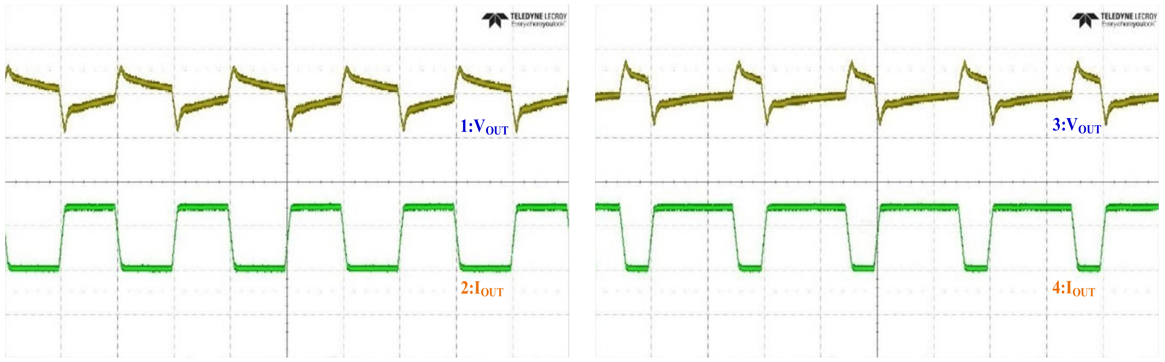
Figure 15 gives the dynamic test results, in the proposed converter, due to the double closed-loop control system, voltage outer loop and current inner loop compensation controller can keep the output voltage and current stable, so as to achieve the power balance of the system.
To verify the correctness of the power feedforward compensation controller, now through the load characteristic change experiment, increase and decrease the input voltage, respectively, and observe the change in the output voltage and the response speed.
Figure 16 show the
response of start-up and close-down, and the output voltage fluctuates within a small range. After a short period of adjustment, the output voltage remains unchanged and reaches a stable state again, which almost becomes a step response, which further proves the feasibility of the control system.
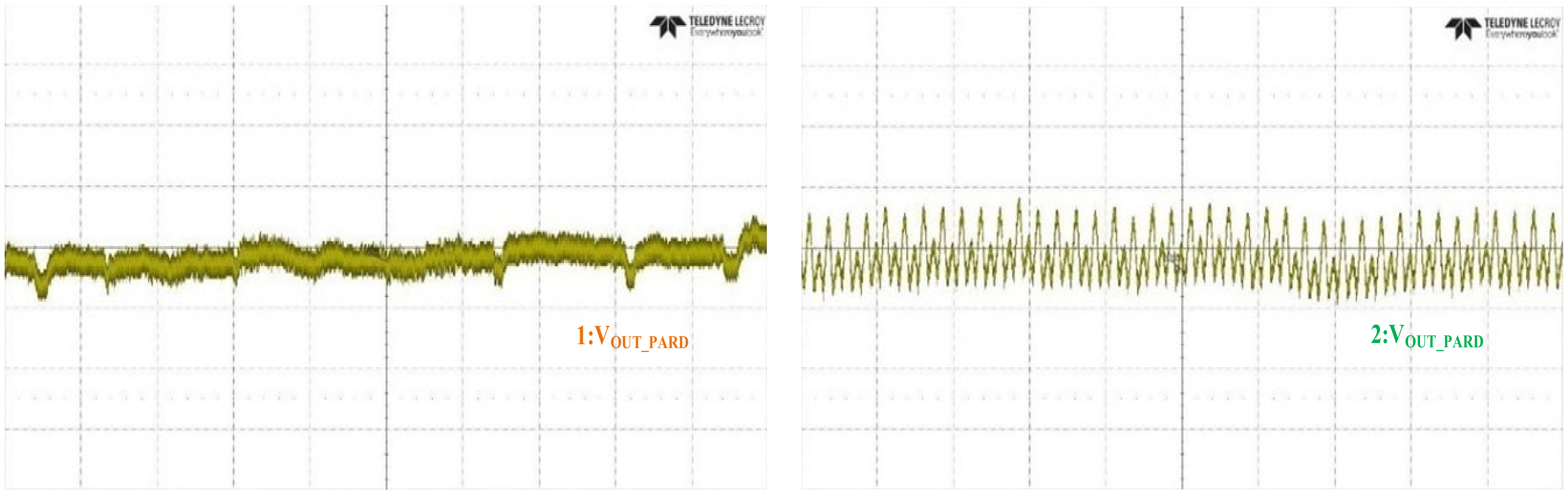
In the full load range,
Figure 17 presents the output periodic and random deviation (PARD) ripple is within 20 mV, it helps meet the EMC requirements of NEEVS.
The efficiency curve of the system with different current levels is shown in
Figure 18. The experimental result is obtained from Power Analyzer YOKOGAWA WT1800. The overall efficiency of the converter is ideal, and peak efficiency can reach nearly 98%.
6. Conclusions
In recent years, the consumption of conventional energy sources has increased dramatically. Due to rising fuel costs and environmental concerns, governments around the world have formulated a series of policies such as strategic planning, technology research and market supervision to promote process of low carbon automobiles, and support the development of the NEEVs industry, the time for the final withdrawal of petrol-powered vehicles from the market is approaching. The NEEVs have important economic and social value in alleviating the energy crisis, save energy, reduce emissions, and promote the development and upgrade of the clean energy industry.
In this paper, the TPIPBi-Buck–Boost converter is proposed and analyzed for new energy electric vehicles applications, which is the core factor of electrical energy flow regulation and management between the battery pack and motor drive inverter within the high voltage direct current bus and convert the voltage from two directions. In the process of starting or accelerating, the electrical energy flows forward to ensure the motor inverter drive performance; during braking or decelerating, the electrical energy flows in reverse to effectively recover the excess electrical energy. The voltage decoupling of battery pack can input and output the most suitable and stable electrical energy according to the drive motor operating conditions. In addition, when the drive motor fails, the TPIPBi-Buck–Boost converter can also effectively block high voltage that may be generated from direct current bus at the end of three phase inverter bridge, so as not to be directly introduced into the battery pack to cause potential risks, thereby improving the safety and reliability of the NEEVs.
The principal configuration and operating states of the converter are determined, and the characteristic waveforms are shown in charge buck, discharge boost, and electric energy interaction modes. The mathematical model based on AC small signal is presented and provides theoretical fundaments of the digital implementation in double closed-loop control system, current inner loop compensation controller, voltage outer loop compensation controller, power feedforward compensation controller and power feedforward compensation controller. The XDPTM Digital Power Controllers XDPP1100-Q040 of Infineon Technologies AG is a highly integrated and fully programmable controller offering optimized solutions, which features optimized power processing blocks and pre-programmed peripherals to enhance the performance of the converter, reduce external components and minimize firmware development effort. The performance of the converter in steady-state and during mode transition is verified by a hardware prototype in laboratory. Therefore, it is foreseeable that this paper could assist with the energy storage management applications of NEEVs.

 ,
, 


