Article

Capacitance Temperature Dependence Analysis of GaN-on-Si Power Transistors

1
Univ. Grenoble Alpes, CEA, Leti, F-38000 Grenoble, France
2
Univ. Lyon, INSA Lyon, Université Claude Bernard Lyon 1, Ecole Centrale de Lyon, CNRS, Ampère, UMR5005, F-69621 Villeurbanne, France
*
Authors to whom correspondence should be addressed.
Energies 2022, 15(19), 7062; https://doi.org/10.3390/en15197062
Submission received: 16 August 2022 / Revised: 16 September 2022 / Accepted: 21 September 2022 / Published: 26 September 2022

Abstract

:
Many kinds of defects are present in the different layers of GaN-on-Si epitaxy. Their study is very important, especially because they play a significant role on the device characteristics. This paper investigates the cause of the temperature dependence of the output and Miller capacitance at three temperatures: 25 °C, 75 °C and 150 °C of GaN-on-Si power transistors. In particular, this study focuses on the temperature dependence of the depletion voltage seen in these characteristics due to the progressive depletion of the two-dimensional electron gas (2DEG) under the device field plates. First, variations of the epitaxial growth are studied, showing that the intrinsic carbon concentration does not play a significant role. Secondly, the deep acceptor trap origin of the temperature dependence is analyzed with a TCAD simulation study. Thirdly, by adjusting TCAD parameters and binding them with experimental concentrations to fit experimental data, trap properties were obtained. The comparison of these properties with the acceptor traps in the literature suggests that the origin is a gallium vacancy tied to oxygen atom(s) on the N site.

1. Introduction

GaN-on-silicon technology is increasingly used to manufacture low-cost lateral AlGaN/GaN power diodes and transistors in the 100 V to 1000 V range [1] for 10 kHz to 100 MHz applications [2]. The high frequency range is achievable because the parasitic capacitance and therefore the charge related (QG, QGD) to the device are very small with respect to its SiC and Si counterparts [3]. As the parasitic capacitance plays a significant role in the switching and especially in the switching losses [4,5,6,7,8], care must be taken to optimize these characteristics to prevent any switching issues [9].
The parasitic capacitance of lateral GaN transistors and diodes are reported to be highly nonlinear due to the capacitive coupling between field plate and the 2DEG that can be depleted in blocking mode as shown in the study of Weiss et al. [10]. The temperature dependence of the characteristics has already been observed in the literature for compact modelling in the Advanced Spice Model for High Electron Mobility Transistor (ASM-HEMT) [11,12] and the MIT Virtual Source GaNFET (MSVG) model [13,14]. Nevertheless, to the authors’ knowledge, the temperature dependence origin has not yet been identified, and its non-linearity has not yet been studied for compact modeling implementation.
In this article, the temperature dependence of the output and Miller capacitance in fully recessed metal insulator semiconductor high electron mobility transistors (MIS-HEMT) fabricated on 200 mm GaN-on-Si epitaxy is studied. Experimental analysis was conducted in parallel with a TCAD study and fitting was performed to extract trap properties whose origin is discussed by comparison with the literature.

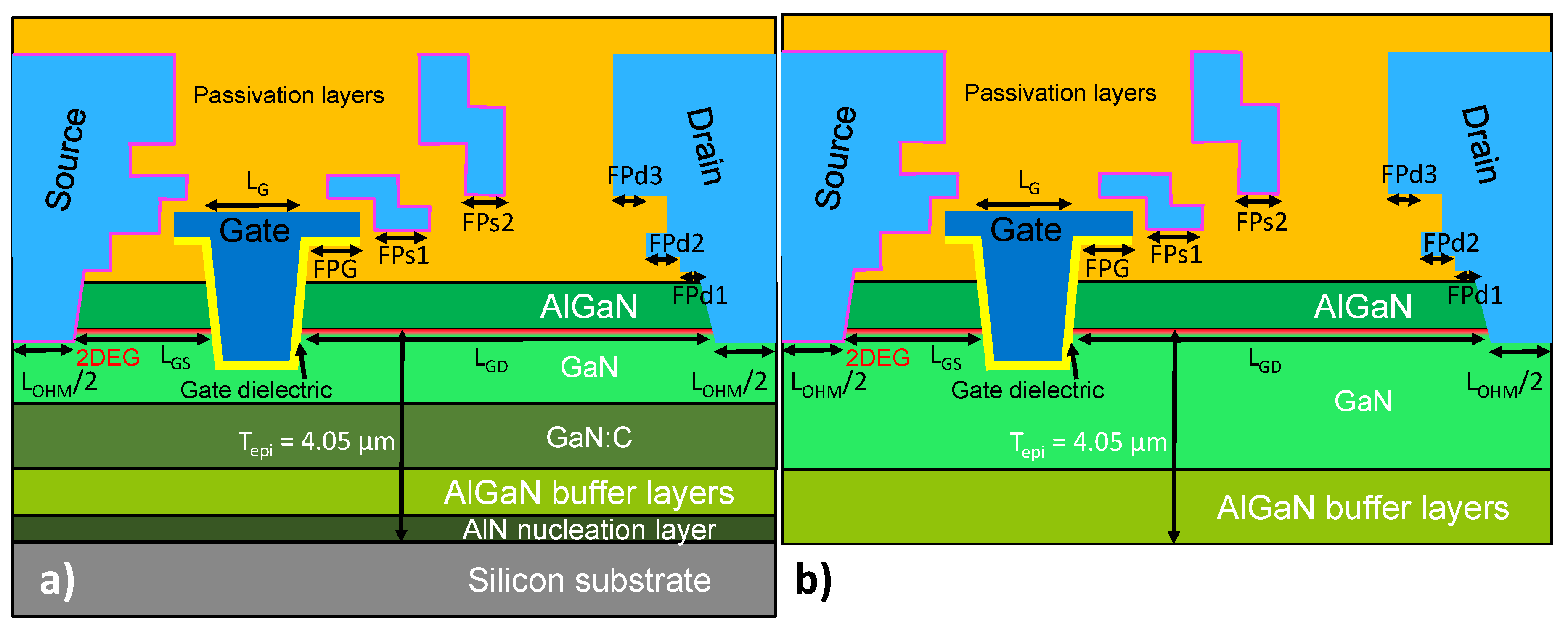
2. Materials and Methods

The power transistor used for this study was fabricated on epitaxial layers grown by Metal Organic Vapor Phase Epitaxy (MOVPE) on an Aixtron® Crius® R200 tool (AIXTRON SE, Herzogenrath, Germany), using 1 mm thick, 200 mm diameter silicon (111) substrates with a resistivity between 3 and 20 Ω.cm. The 4.05 µm thick epitaxial structure was composed of five different parts: an AlN nucleation layer, AlxGa1-xN Strain Relief Layers (SRL), a GaN:C layer, the active AlGaN/AlN/GaN layers and finally an in situ Si3N4 layer to protect the hetero-junction. This epitaxy is designed to withstand voltage higher than 1000 V. To ensure the normally-off operation, a fully recessed MIS gate was made by etching the AlGaN/AlN/GaN layers with an Atomic Layer Etching (ALE) process. After cleaning the surface, the alumina gate dielectric was deposited by Atomic Layer Deposition (ALD) and covered by TiN/W gate metal layers. Next, low temperature Ti/Al Ohmic contacts were formed on both side of the gate in direct contact with the 2DEG. Consecutive metallizations and passivations ended the process to build the field plate structure illustrated in Figure 1 composed of six field plates: FPG, FPs1, FPs2, FPd1, FPd2, and FPd3. The source deported stepped field plates named FPs1 and FPs2 protect the gate. The four other field plates are designed for the electric field distribution tailoring to meet the low current collapse and the breakdown voltage specification. This field plate system allows the transistor to withstand at least 650 V in blocking mode [15].
To simulate this device, Synopsys® SentaurusTM [16] (Synopsys, San Jose, United States) was used. The experimental transistor design and buffer layers were implemented with a few minor changes. Figure 1a,b show the differences between the true structure and the TCAD model, and we see that the silicon has been removed, and the AlGaN buffer layers and AlN nucleation layer have been simplified into AlGaN buffer layers. This choice allows saving convergence time while being able to reproduce experimental data with a grounded substrate. Concerning the device physics, the piezoelectric polarization strain model with Vurgaftman values [17] was used for the calculation of spontaneous and piezoelectric polarization effect. This model was activated only at the AlGaN/Si3N4 interface and at the GaN/AlN/AlGaN interfaces because the strain in the buffer layers evolves strongly during growth [18] and is quite challenging to model accurately. In addition, the activation of this model was tuned to fit the electron density in the 2DEG. At the AlGaN/Si3N4 interface, surface donors with a concentration of 5 × 1013 cm−2 at an energy level of 1.6 eV [19,20] below the conduction band were implemented to compensate for the polarization charges at this interface. Other traps were introduced in the epitaxy as detailed in the next section.
The electrical measurements of the experimental study were performed with the Keysight® B1505 (Keysight, Santa Rosa, United States) coupling the Multi-Frequency Capacitance Measurement Unit (MFCMU) and the High-voltage Source Measurement Unit (HV SMU). A DC voltage sweep from 0 V to 200 V with a step of 2 V was applied at the drain. The DC and AC signals were mixed with the N1260A Bias Tee. The integration time was done over two power line cycles (PLC). To choose the proper ramp rate, the delay time was tuned with time monitoring during the whole sweep: 1 ms for 7 V/s and 360 ms for 3 V/s.
A preliminary study was conducted on a test wafer to check the impact of the epitaxial growth rate (GR) of the GaN:C layer on atomic distributions with Secondary Ion Mass Spectroscopy (SIMS). The different tested GaN:C epitaxial growth rates are those present on the wafers used for the studied devices in this article: 5.8 µm/h and 10 µm/h. The results of this study are summarized in Table 1. As the carbon concentration decreases exponentially with depth, only the bottom and top concentration are reported. It can be observed that the intrinsic carbon content that is brought by the trimethylgallium (TMGa) precursor increases by roughly a factor three with the growth rate. Concerning the other species present in the epitaxy, Table 1 shows that the oxygen concentration is reported to be constant whatever the growth rate and is between 0.3 to 0.5 a.u. in the GaN buffer (GaN:C and GaN in Figure 1a), whereas, in the III-V buffer (AlGaN buffer layers and AlN nucleation layer in Figure 1a), it is roughly equal to 1 a.u. This is a worthwhile element for the next section. Hydrogen is also present in the epitaxy thanks to the TMGa, trimethylalluminium (TMAl) and ammonia (NH3) precursors. Its concentration is between that of carbon and oxygen.
The experimental temperature dependence was studied with the following proposed methodology. In a first experimental part, the GaN:C epitaxial growth rate was changed to indirectly assess the role of the intrinsic carbon concentration. The drain to source sweep rate was varied to give information about the trap kinetics. In a second part, the qualitative impact of deep acceptor traps in the epitaxy on the capacitance characteristic was analyzed by TCAD, and finally, trap energy EA and the trap cross-section σP were adjusted to fit the experimental data. By comparing these parameters to the literature, a possible origin of the deep acceptor trap was found.
This study was performed on the Miller capacitance: CRSS. The output capacitance: COSS was not studied since both depend on the 2DEG depletion and so the results are expected to be similar. The measurements were conducted with the gate biased in order to have a voltage between the gate and the source (VGS) equal to −2 V. The small signal has a frequency of 1 MHz and an amplitude of 40 mV and all the measurements occurred without illumination and with a grounded substrate.

3. Results

3.1. Experimental Study

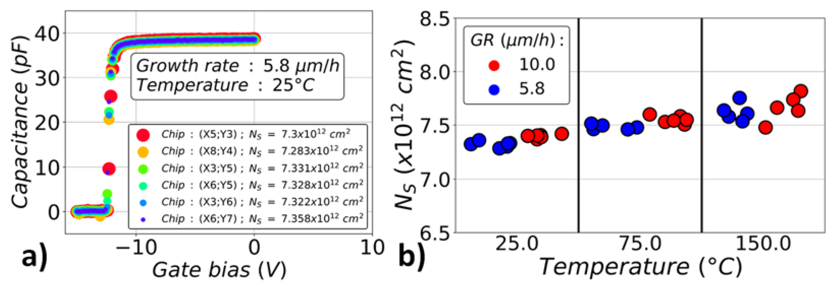
3.1.1. GaN:C Epitaxial Growth Rate (GR) Dependence

To begin with, Figure 2a shows the non-linear capacitance versus voltage at three different temperatures with three voltage drops corresponding to depletion voltages. A depletion voltage is defined as the voltage for which the 2DEG is completely depleted under a field plate [10]. For instance, the first one corresponds to the complete depletion of the 2DEG under the gate field plate with the length FPG in Figure 1a, the second one under the first source field plate (FPs1 in Figure 1a) and so on and so forth. The temperature dependence is visible on the depletion voltages with the most prominent dependence on the third depletion voltage. Therefore, the parameter used in this article to study the temperature dependence is the voltage for which the capacitance is equal to 0.005 pF/mm.
The capacitance temperature dependence was studied as a function of the GaN:C epitaxial growth rate: 5.8 µm/h and 10 µm/h at a fixed sweep rate of 3 V/s. In Figure 2a, the raw capacitance of representative transistors (transistors having a median behavior among the tested transistors) is plotted. As the temperature rises, the depletion voltage decreases. The only significant difference between the two GaN:C epitaxial growth rates is visible at 25 °C where the depletion voltage is higher in the case of 5.8 µm/h. This means that the induced change of carbon concentration shown in Table 1 is probably not correlated with the observed temperature dependence. Both behaviors are confirmed on several devices as can be seen in Figure 2b.
According to the formula given by Ishida et al. [21], the depletion voltage should be proportional to the sheet charge that is depleted in the GaN layer: the 2DEG sheet density. Indeed, by considering that a field plate structure locally depletes the 2DEG underneath it thanks to its capacitive coupling, as explained by Weiss et al. [10], the formula can be applied. To extract the electron sheet density, NS, capacitive measurements, on a 200 × 200 µm2 Gated Van Der Pauw (VDP) structure, were performed. Schematic cross-section of the test structure is shown in Figure 4 of [22]. They were performed with a small signal of 40 mV and a frequency of 1 kHz. Integrating the obtained capacitance versus voltage characteristic in Figure 3a from −15 V to 0 V allows the extraction of the electron density. The NS for every temperature and GaN:C epitaxial growth rate are summarized in Figure 3b. The NS is shown to be independent of the growth rate and is quasi-constant with temperature. Thus, by contrast with what is expected from the formula given by Ishida et al. [21] for an ideal device, depletion voltage decreasing trend with temperature, shown in Figure 2b, cannot be related to the variation of the electron density.

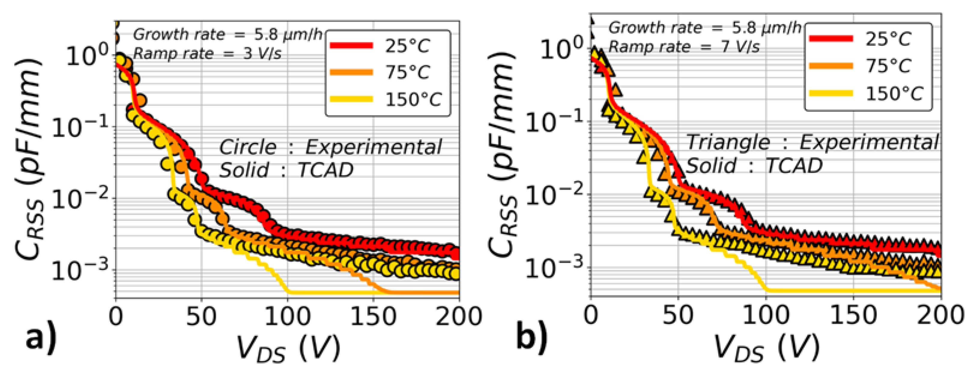
3.1.2. Ramp Rate (RR) Dependence

In this part, the capacitance temperature dependence was studied as a function of the ramp rate: 3 V/s and 7 V/s at a fixed GaN:C epitaxial growth rate of 5.8 µm/h. In Figure 4a, the raw capacitance of representative transistors (transistors having a median behavior among the tested transistors) is plotted. The only significant effect is visible at 75 °C: the depletion voltage decreases when the ramp rate is reduced. This is confirmed on several devices, as can be seen in Figure 4b. Thus, the studied trend is found to depend on time and temperature as in the case of trapping kinetics. This is why in the next part, in TCAD simulation, the qualitative impact of deep acceptor traps will be studied.

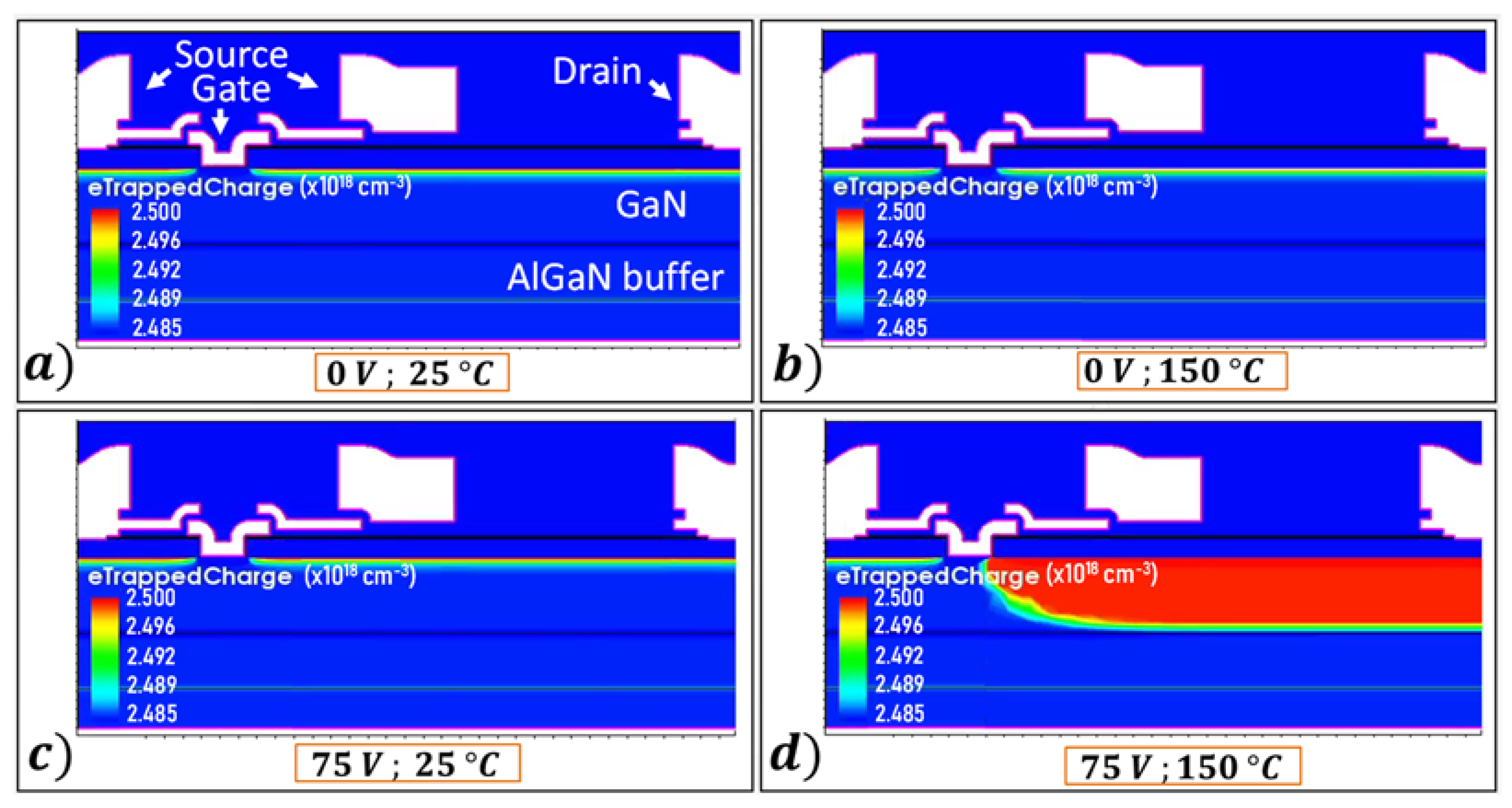
3.2. TCAD Simulation Study

The TCAD simulation of the studied structure allows the simulation of the impact of deep acceptor traps on the capacitance characteristics. In this sub-section, deep acceptor traps are introduced within the well-known partial auto-compensation model [23]. In this model, deep acceptor traps at an energy of around 0.9 eV (from the valence band) are coupled with shallow donor traps at an energy of 0.11 eV (from the conduction band). The model is used to simulate AlGaN/GaN devices [24,25,26] because it reproduces the semi-insulating properties of carbon doped GaN layers as described by Uren et al. [27] to explain the current collapse dynamic [28,29,30], the electric field dynamic variation [31], threshold voltage instabilities [32], and backgating transient measurement [33]. The deep acceptor traps are related to the carbon in N-site: CN because it was shown to be at 0.9 eV from the valence band based on calculation with the generalized Kohn–Sham scheme and the hybrid functional of Heyd, Scuseria and Ernzerhof (HSE). In this article, the origin of deep acceptor traps is detailed and discussed in Section 3.3 and Section 3.4.
These deep acceptor traps and shallow donor traps are uniformly distributed in the AlGaN buffer layers illustrated in Figure 1b and in the equivalent place of the GaN:C in Figure 1a with a constant concentration [A] and [D], respectively. They show energies EA and ED with cross-sections σ A , h + and σ D , e for holes: h+ or electrons: e- respectively. σ D , e is kept constant and equal to 1 × 10⁻¹⁵ cm2.
In this subsection, the piezoelectric model was activated at 77% in order to obtain the experimental value of the electron density in the 2DEG at 25 °C with a GaN:C epitaxial growth rate of 5.8 µm/h: 7.35 × 1012 cm−2, as shown in Figure 3b. The partial auto-compensation model is used with a high compensation value in our epitaxy. The initial value of the compensation used for this qualitative study was 99.4%, as in [33]. The combination of acceptor and donor traps gives an approximate trap concentration of 5 × 1018 cm−3.
To understand how the different trap parameters affect the capacitance temperature dependence, the different splits presented in Table 2 are compared in simulation with a ramp rate of a 3 V/s. First, the capacitance characteristic at different temperatures is analyzed as a function of the deep acceptor traps energy (splits 1, 2 and 3) to show how the trap ionization impacts the capacitance temperature dependence. Secondly, by comparing splits 2, 4 and 5, the impact of the donor trap density is studied to confirm the presented temperature dependence explanation. A closer look at the concentration dependence keeping [A] − [D] constant will be analyzed with splits 5 and 8 to demonstrate that this is the important quantity that must be mentioned when dealing with a compensation model. Finally, with the splits 5, 6 and 7, the cross-section dependence is analyzed to assess its impact on the depleted voltage temperature variation.

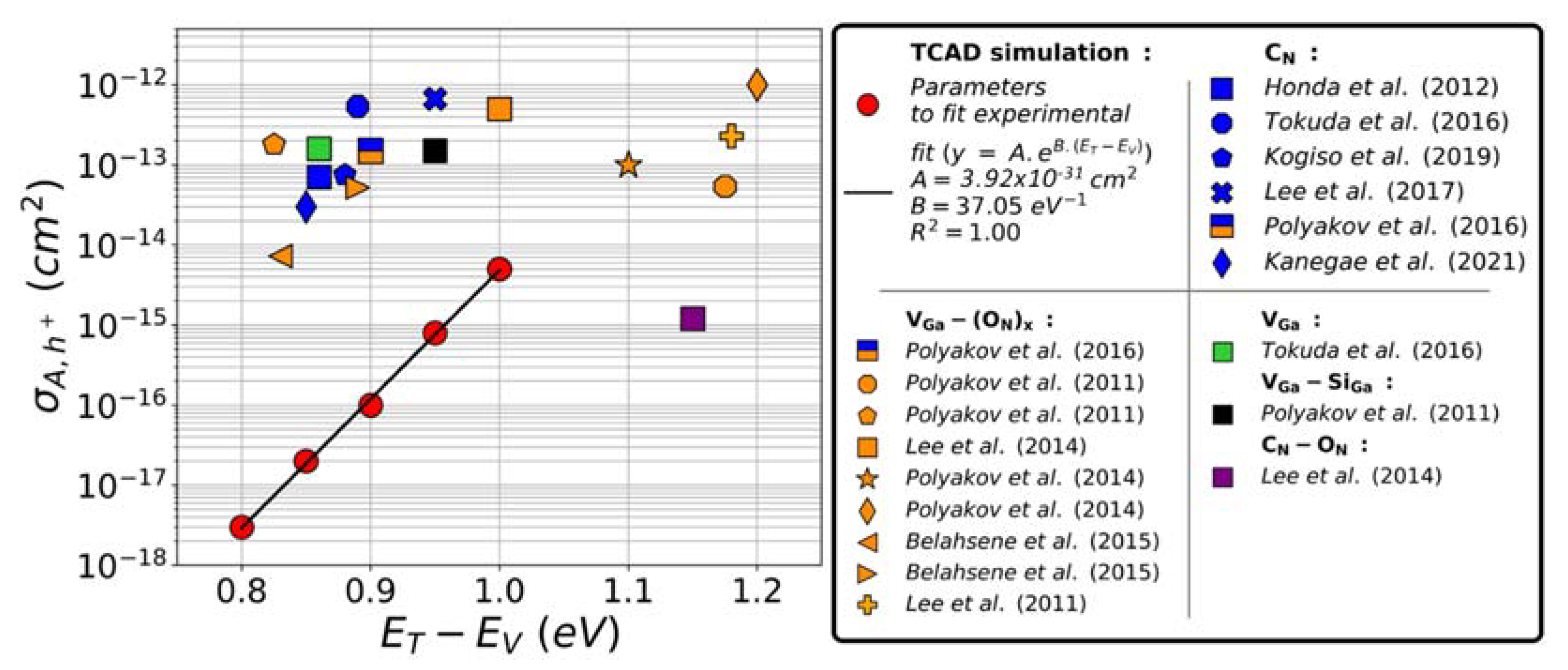
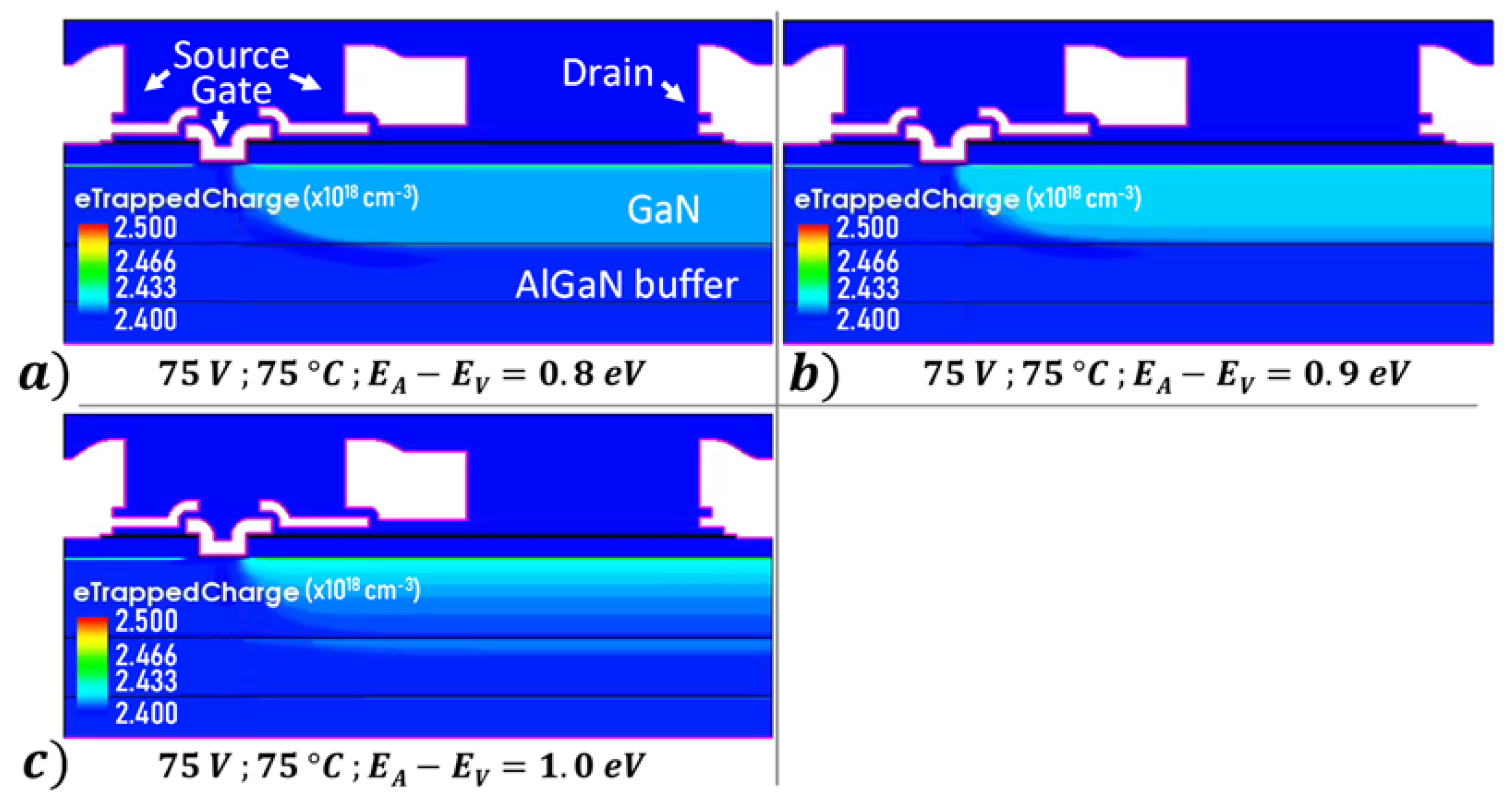
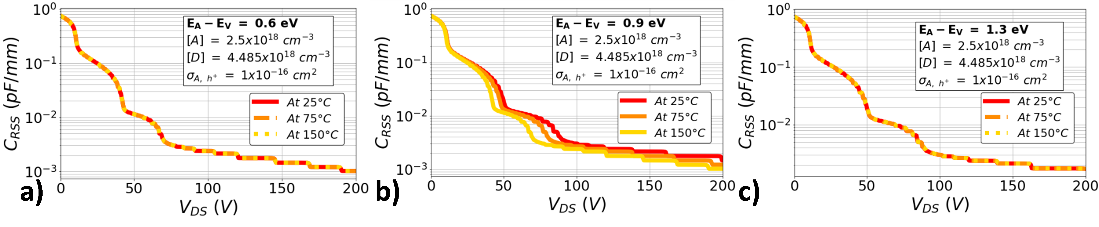
3.2.1. The Deep Acceptor Traps Energy Dependence

In Figure 5, the Miller capacitance was plotted against reverse bias at three temperatures on each graph for three different acceptor trap energies (5a,b,c). The temperature dependence is visible at a trap energy of 0.9 eV. Moreover, the depletion voltage is reduced with temperature as in the experimental data. By contrast, for 0.6 eV and 1.3 eV, no dependence is seen.
By looking at the evolution of the acceptor trap ionization with temperature and the drain voltage for split 2 in Figure 6, a hypothesis on the contribution of the excess acceptor trap ionization on the 2DEG depletion can be deduced. The excess ionized acceptor traps are defined as the ionized acceptor traps that are not compensated by the ionized donor traps, which is what is displayed with the colormap in Figure 6. Indeed, it is shown that whatever the temperature for 0 V, when the drain is biased at 75 V at 25 °C, the excess ionized acceptor traps are distributed at the interface between the equivalent “GaN:C” region and the top GaN layer, creating a negative charge layer, whereas when the drain is 75 V biased at 150 °C, the excess ionized acceptor traps are spread in all the buffer layers between the gate and the drain. Therefore, to keep the overall electrostatic equilibrium with respect to the 25 °C condition at 75 V, charges in the 2DEG have to be removed, resulting in a more depleted 2DEG at the same voltage. The ionization of an excess of deep acceptors with respect to the already ionized shallow donor traps can therefore explain the reduced depletion voltage when the temperature is increased.

3.2.2. The Trap Concentration Dependence

Figure 7a illustrates the temperature variation of the third depletion voltage: V3 while varying the donor traps concentration from 2.4 × 1018 cm−3 to 2.485 × 1018 cm−3 at a fixed acceptor trap concentration of 2.5 × 1018 cm−3 (splits 2, 4 and 5 in Table 2). It is shown that the temperature dependence of the depletion voltage increases with reducing donor trap concentration. This confirms the hypothesis of excess acceptor trap ionization. Indeed, by decreasing the donor trap ionization, the excess acceptor trap concentration that can be ionized increases. Moreover, in Figure 7a, at 25 °C the depletion voltage is the same whatever the concentration of donors, which means that no excess acceptor traps are ionized at this temperature.
In addition, by keeping [A] − [D] constant and equal to 1 × 1017 cm−3 and by increasing the total trap density: [A] + [D] from 0.99 × 1019 cm−3 (split 5 in Table 2) to 3.99 × 1019 cm−3 (split 8 in Table 2), it can be clearly seen in Figure 7b that the capacitance temperature dependence is unchanged.
The last two observations confirm that it is the difference of ionization depending on the trap properties that is responsible for the temperature dependence and not only the difference between the acceptor and donor trap concentrations. We note that since the donors are at a sufficiently shallow energy level, they are entirely ionized.

3.2.3. The Deep Acceptor Trap Hole Cross-Section Dependence

Figure 7c investigates the deep acceptor trap hole cross-section impact on the third depletion voltage (V3) temperature dependence. It varies from 1 × 10⁻¹⁷ cm2 to 1 × 10⁻¹⁵ cm2 (splits 5, 6 and 7 in Table 2). At 150 °C, there is no dependence, which shows that all the excess acceptor traps are ionized. By contrast, at 75 °C, the higher the cross-section, the lower the depletion voltage. This makes sense because at a given bias and temperature, by increasing the cross-section, the probability of an acceptor trap being ionized rises, shifting the depletion voltage to a lower value. Finally, at 25 °C, there is a small decrease because the temperature dependence is probably shifted at a lower temperature range.
Thus, three conclusions arise from this qualitative study. (1) The negative temperature dependence of depletion voltages of transistor capacitance characteristics occurs due to the ionization of excess deep acceptor traps with respect to shallow donor traps. (2) The deep acceptor traps’ energy level and their hole cross-section both determine together if there is a temperature dependence between 25 °C and 150 °C. Finally, (3) the excess ionized acceptor trap concentration determines the amplitude of the dependency.

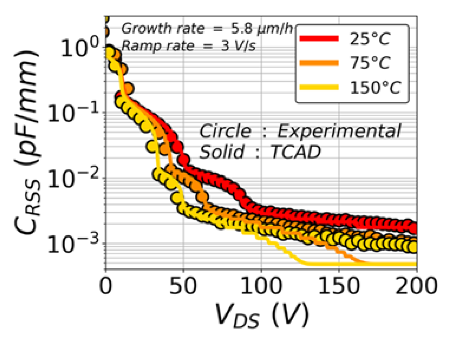
3.3. TCAD Fit with the Experimental Study

A fit with the experiment was obtained at the ramp rate of 3 V/s in Figure 8a and verified at 7 V/s in Figure 8b to validate the trap kinetics. The fits were obtained with a difference between the deep acceptor traps and the shallow donor traps concentration: [A] − [D] of 1 × 1017 cm−3, which is not new with respect to the literature [26,33,34] and with an acceptor trap energy of 0.9 eV coupled with a hole cross-section of 1 × 10⁻¹⁶ cm2.
Nevertheless, the fit is not perfect after the third depletion voltage and especially at 75 °C and 150 °C for voltages higher than 100 V. Indeed, it seems that the 2DEG is depleted faster in the simulation, thus reaching the high-voltage constant capacitance faster at high temperature. This difference may be due to the non-uniform distribution of traps in our samples, as will be presented below.
To be exhaustive on the possible fitting parameters: acceptor trap energy and acceptor trap hole cross-section, fits were made with the acceptor traps energy of 0.8, 0.85, 0.95 and 1.0 eV (not shown here). The obtained hole cross-sections combined with the trap energies allow building an exponential relationship, shown in Figure 9. Then, by comparing the exponential relationship with the deep acceptor traps properties reported in the literature [35,36,37,38,39,40,41,42,43,44,45] (see Figure 9) in the energy 0.8 to 1.0 eV energy range, it seems that hypothesis involving only carbon on the N-site: CN or gallium vacancy alone: VGa or tied to a silicon atom on the Ga-site: VGa-SiGa can be discarded because the trap hole cross section mismatch is too large. The remaining hypotheses involve oxygen as the gallium vacancy with oxygen atom(s) on the N-site: VGa-(ON)x traps proposed by Polyakov et al. [43] and Lee et al. [45]. The validity of this hypothesis will be verified in the next part.

3.4. VGa-(ON)x Hypothesis Verification

Making a fit in the 1.0 to 1.2 eV energy range while keeping the choice of the acceptor and donor trap concentration arbitrary (with [A] − [D] constant and equal to 1 × 1017 cm−3) was not possible. Indeed, the choice of the absolute concentration matters in this energy range on the position of the depletion voltage at 75 °C as the hole cross-section. This is probably explained by the excess acceptor traps’ ionization distribution, as shown in Figure 10. In fact, by looking at their distribution in the 0.8 to 1.0 eV energy range with hole cross-section chosen accordingly to make a fit with the experimental data, when the energy approaches 1.0 eV, the excess acceptor traps ionization distribution becomes non-uniform with a maximum at the top of the distribution. Our hypothesis is, as long as the excess acceptor traps’ ionization distribution is roughly constant, the qualitative study made previously is valid.
The previous findings found that the remaining hypothesis for deeper traps are associated with oxygen, and the absolute acceptor trap concentration can be bound by the oxygen concentration found in the SIMS in the preliminary wafer, reported in Table 1, while [A] – [D] is kept equal to 1 × 1017 cm−3. There is approximately 1 a.u. of oxygen in the AlxGa1-xN buffer layers and from 0.3 to 0.5 a.u. in the GaN:C. Thus, the fit was verified in Figure 11 with the quantity [A] equal to 1 a.u. in the AlxGa1-xN buffer layers and 0.5 a.u. in the GaN, except for the last 200 nm (supposed unintentionally doped without traps). It was done with the energy of 1.1 eV and the hole cross-section of 1 × 10⁻¹³ cm2 as in the article of Polyakov et al. [43]. Thus, gallium vacancy with oxygen atom(s) on the N-site could be the origin of the capacitance temperature dependence of the studied transistors.
Moreover, Figure 11 with respect to Figure 8a proposes a better fit. That is why, earlier on, the non-uniformity in the trap distribution is the proposed hypothesis for the mismatch between experimental data and simulation at 75 °C and 150 °C for voltages higher than 100 V.

4. Conclusions

In this study, the temperature dependence of the output and Miller capacitance of fully recessed AlGaN/GaN MIS-HEMT made on a 200 mm GaN-on-Si epitaxy was studied. In particular, the depletion voltage temperature dependence at three different temperatures (25 °C, 75 °C and 150 °C) was analyzed. This was done thanks to experimental measurement correlated with TCAD simulations. The experimental part demonstrated that this dependence is neither linked to the GaN:C epitaxial growth rate nor to the electron density in the channel. This means that the induced change of carbon content could not be correlated with the studied capacitance temperature dependence. Nevertheless, the variation of the bias sweep ramp rate revealed the time dependence of the depletion voltage. This, in addition to the temperature dependence, demonstrated the trap origin. The qualitative TCAD study focused on the buffer traps showed that the temperature dependence is due to the deep acceptor traps excess with respect to the shallow donor traps. The acceptor traps’ energy level and the acceptor traps’ hole cross-section together determine the temperature range for which the temperature dependence will be visible on the depletion voltage, whereas the excess ionized acceptor trap concentration determines the amplitude of this dependence. Finally, adjustment of the TCAD traps parameters was conducted to obtain the proper hole cross-section for a given acceptor trap’s energy in order to fit experimental data in the 0.8 to 1.0 eV range. This led to the exponential relationship between both quantities. The huge mismatch between this trend and the literature discarded some defects from the origin hypothesis (especially the carbon related one). Finally, using deeper trap level properties reported in the literature and bounding trap concentration to the oxygen one found in SIMS, the acceptor trap origin may be a Gallium vacancy tied to oxygen atom(s) in N site.

Author Contributions

Conceptualization, F.R.-M.; data curation, F.R.-M., J.B. and M.C.; formal analysis, F.R.-M.; investigation, F.R.-M. and E.R.; methodology, F.R.-M.; supervision, J.B., W.V., M.C., H.M., D.P., R.G., C.G. and V.S.; writing—original draft, F.R.-M.; writing—review and editing, F.R.-M., J.B., W.V., M.C., M.-A.J., E.R., H.M., D.P., R.G., C.G. and V.S. All authors have read and agreed to the published version of the manuscript.

Funding

This work was partially supported by the French Public Authorities within the frame of the PSPC French national program «G-Mobility»: DOS0134974.

Institutional Review Board Statement

Not applicable.

Informed Consent Statement

Not applicable.

Data Availability Statement

Data is contained within the article.

Conflicts of Interest

The authors declare no conflict of interest.

References

  1. Stephen, O.; Dan, K. The GaN revolution in fast charging and power conversion. In Aspencore Guide to Gallium Nitride: A New Era for Power Electronics; Aspencore: Ebersberg, Germany, 2021. [Google Scholar]
  2. Di Paolo, M.E. Markets Turn to Wide-Bandgap Semiconductors to Increase Power Efficiency. EE Times Europe, 8 June 2020. [Google Scholar]
  3. Jimmy, L. Webinar: GaN Performance Advantage in Totem Pole PFC and LLC Converters; GaN Systems: Ottawa, ON, Canada, 2020. [Google Scholar]
  4. Hou, R.; Lu, J.; Chen, D. Parasitic Capacitance eqoss loss mechanism, calculation, and measurement in hard-switching for GaN HEMTs. In Proceedings of the 2018 IEEE Applied Power Electronics Conference and Exposition (APEC), San Antonio, TX, USA, 4–8 March 2018; pp. 919–924. [Google Scholar] [CrossRef]
  5. Zulauf, G.; Tong, Z.; Plummer, J.D.; Rivas-Davila, J.M. Active Power Device Selection in High- and Very-High-Frequency Power Converters. IEEE Trans. Power Electron. 2019, 34, 6818–6833. [Google Scholar] [CrossRef]
  6. Guacci, M.; Heller, M.; Neumayr, D.; Bortis, D.; Kolar, J.W.; Deboy, G.; Ostermaier, C.; Haberlen, O. On the Origin of the COSS-Losses in Soft-Switching GaN-on-Si Power HEMTs. IEEE J. Emerg. Sel. Topics Power Electron. 2019, 7, 679–694. [Google Scholar] [CrossRef]
  7. Nikoo, M.S.; Jafari, A.; Perera, N.; Matioli, E. New Insights on Output Capacitance Losses in Wide-Band-Gap Transistors. IEEE Trans. Power Electron. 2020, 35, 6663–6667. [Google Scholar] [CrossRef]
  8. Nikoo, M.S.; Jafari, A.; Perera, N.; Matioli, E. Output Capacitance losses in wide-band-gap transistors: A small-signal modeling approach. In Proceedings of the 2020 32nd International Symposium on Power Semiconductor Devices and ICs (ISPSD), Vienna, Austria, 13–18 September 2020; pp. 190–193. [Google Scholar] [CrossRef]
  9. Toshiba Electronic Devices & Storage Corporation. Application Note: MOSFET Self-Turn-On Phenomenon; Toshiba: Tokyo, Japan, 2018. [Google Scholar]
  10. Weiss, B.; Reiner, R.; Waltereit, P.; Quay, R.; Ambacher, O. Analysis and Modeling of GaN-based multi field plate schottky power diodes. In Proceedings of the 2016 IEEE 17th Workshop on Control and Modeling for Power Electronics (COMPEL), Trondheim, Norway, 27–30 June 2016; pp. 1–6. [Google Scholar] [CrossRef]
  11. Aamir Ahsan, S.; Ghosh, S.; Sharma, K.; Dasgupta, A.; Khandelwal, S.; Chauhan, Y.S. Capacitance Modeling in Dual Field-Plate Power GaN HEMT for Accurate Switching Behavior. IEEE Trans. Electron Devices 2016, 63, 565–572. [Google Scholar] [CrossRef]
  12. Ahsan, S.A. Modeling and Analysis of GaN HEMTs for Power-Electronics and RF Applications. Ph.D. Thesis, Department of Electrical Engineering Indian Institute of Technology Kanpur, Kanpur, India, 2017. [Google Scholar]
  13. Radhakrishna, U. Modeling Gallium-Nitride Based High Electron Mobility Transistors: Linking Device Physics to High Voltage and High Frequency Circuit Design. Ph.D. Thesis, Massachusetts Institute Of Technology, Cambridge, MA, USA, 2016. [Google Scholar]
  14. Radhakrishna, U.; Imada, T.; Palacios, T.; Antoniadis, D. MIT Virtual Source GaNFET-High Voltage (MVSG-HV) Model: A Physics Based Compact Model for HV-GaN HEMTs: MIT Virtual Source GaNFET-High Voltage (MVSG-HV) Model: A Physics Based Compact Model for HV-GaN HEMTs. Phys. Status Solidi C 2014, 11, 848–852. [Google Scholar] [CrossRef]
  15. Royer, C.L.; Mohamad, B.; Biscarrat, J.; Vauche, L.; Escoffier, R.; Buckley, J.; Bécu, S.; Riat, R.; Gillot, C.; Charles, M.; et al. (Accepted Abstract) Normally-OFF 650V GaN-on-Si MOSc-HEMT Transistor: Benefits of the Fully Recessed Gate Architecture. In Proceedings of the 2022 IEEE 34th International Symposium on Power Semiconductor Devices and ICs (ISPSD), Vancouver, BC, Canada, 22–25 May 2022; p. 3. [Google Scholar]
  16. Synopsys TCAD Tools, R-2020.09, no Availble Website for this Release. Available online: https://www.synopsys.com/silicon/tcad.html (accessed on 20 September 2022).
  17. Vurgaftman, I.; Meyer, J.R. Band Parameters for Nitrogen-Containing Semiconductors. J. Appl. Phys. 2003, 94, 3675–3696. [Google Scholar] [CrossRef]
  18. Charles, M.; Mrad, M.; Kanyandekwe, J.; Yon, V. Extraction of Stress and Dislocation Density Using In-Situ Curvature Measurements for AlGaN and GaN on Silicon Growth. J. Cryst. Growth 2019, 517, 64–67. [Google Scholar] [CrossRef]
  19. Ibbetson, J.P.; Fini, P.T.; Ness, K.D.; DenBaars, S.P.; Speck, J.S.; Mishra, U.K. Polarization Effects, Surface States, and the Source of Electrons in AlGaN/GaN Heterostructure Field Effect Transistors. Appl. Phys. Lett. 2000, 77, 250–252. [Google Scholar] [CrossRef]
  20. Jang, H.W.; Jeon, C.M.; Kim, K.H.; Kim, J.K.; Bae, S.-B.; Lee, J.-H.; Choi, J.W.; Lee, J.-L. Mechanism of Two-Dimensional Electron Gas Formation in AlxGa(1−x)N/GaN Heterostructures. Appl. Phys. Lett. 2002, 81, 1249–1251. [Google Scholar] [CrossRef]
  21. Ishida, H.; Shibata, D.; Yanagihara, M.; Uemoto, Y.; Matsuo, H.; Ueda, T.; Tanaka, T.; Ueda, D. Unlimited High Breakdown Voltage by Natural Super Junction of Polarized Semiconductor. IEEE Electron Device Lett. 2008, 29, 1087–1089. [Google Scholar] [CrossRef]
  22. Lorin, T.; Vandendaele, W.; Gwoziecki, R.; Baines, Y.; Biscarrat, J.; Jaud, M.-A.; Gillot, C.; Charles, M.; Plissonnier, M.; Ghibaudo, G.; et al. On the Understanding of Cathode Related Trapping Effects in GaN-on-Si Schottky Diodes. IEEE J. Electron Devices Soc. 2018, 6, 956–964. [Google Scholar] [CrossRef]
  23. Meneghini, M.; Meneghesso, G.; Zanoni, E. Power GaN devices: Materials, applications and reliability. In Power Electronics and Power Systems; Springer: Cham, Switzerland, 2017; ISBN 978-3-319-43197-0. [Google Scholar]
  24. Zagni, N.; Chini, A.; Puglisi, F.M.; Pavan, P.; Verzellesi, G. On the Modeling of the Donor/Acceptor Compensation Ratio in Carbon-Doped GaN to Univocally Reproduce Breakdown Voltage and Current Collapse in Lateral GaN Power HEMTs. Micromachines 2021, 12, 709. [Google Scholar] [CrossRef] [PubMed]
  25. Zagni, N.; Chini, A.; Puglisi, F.M.; Pavan, P.; Verzellesi, G. The Effects of Carbon on the Bidirectional Threshold Voltage Instabilities Induced by Negative Gate Bias Stress in GaN MIS-HEMTs. J. Comput. Electron. 2020, 19, 1555–1563. [Google Scholar] [CrossRef]
  26. Joshi, V.; Tiwari, S.P.; Shrivastava, M. Part I: Physical Insight Into Carbon-Doping-Induced Delayed Avalanche Action in GaN Buffer in AlGaN/GaN HEMTs. IEEE Trans. Electron Devices 2019, 66, 561–569. [Google Scholar] [CrossRef]
  27. Uren, M.J.; Karboyan, S.; Chatterjee, I.; Pooth, A.; Moens, P.; Banerjee, A.; Kuball, M. “Leaky Dielectric” Model for the Suppression of Dynamic RON in Carbon-Doped AlGaN/GaN HEMTs. IEEE Trans. Electron Devices 2017, 64, 2826–2834. [Google Scholar] [CrossRef]
  28. Uren, M.J.; Silvestri, M.; Casar, M.; Hurkx, G.A.M.; Croon, J.A.; Sonsky, J.; Kuball, M. Intentionally Carbon-Doped AlGaN/GaN HEMTs: Necessity for Vertical Leakage Paths. IEEE Electron Device Lett. 2014, 35, 327–329. [Google Scholar] [CrossRef]
  29. Iucolano, F.; Parisi, A.; Reina, S.; Patti, A.; Coffa, S.; Meneghesso, G.; Verzellesi, G.; Fantini, F.; Chini, A. Correlation between dynamic rdsou transients and carbon related buffer traps in AlGaN/GaN HEMTs. In Proceedings of the 2016 IEEE International Reliability Physics Symposium (IRPS), Pasadena, CA, USA, 17–21 April 2021. [Google Scholar] [CrossRef]
  30. Zagni, N.; Chini, A.; Puglisi, F.M.; Pavan, P.; Verzellesi, G. The Role of Carbon Doping on Breakdown, Current Collapse, and Dynamic On-Resistance Recovery in AlGaN/GaN High Electron Mobility Transistors on Semi-Insulating SiC Substrates. Phys. Status Solidi A 2020, 6, 1900762. [Google Scholar] [CrossRef]
  31. Uren, M.J.; Caesar, M.; Karboyan, S.; Moens, P.; Vanmeerbeek, P.; Kuball, M. Electric Field Reduction in C-Doped AlGaN/GaN on Si High Electron Mobility Transistors. IEEE Electron Device Lett. 2015, 36, 826–828. [Google Scholar] [CrossRef]
  32. Meneghesso, G.; Silvestri, R.; Meneghini, M.; Cester, A.; Zanoni, E.; Verzellesi, G.; Pozzovivo, G.; Lavanga, S.; Detzel, T.; Haberlen, O.; et al. Threshold voltage i0nstabilities in D-Mode GaN HEMTs for power switching applications. In Proceedings of the 2014 IEEE International Reliability Physics Symposium, Waikoloa, HI, USA, 1–5 June 2014. [Google Scholar] [CrossRef]
  33. Chini, A.; Meneghesso, G.; Meneghini, M.; Fantini, F.; Verzellesi, G.; Patti, A.; Iucolano, F. Experimental and Numerical Analysis of Hole Emission Process From Carbon-Related Traps in GaN Buffer Layers. IEEE Trans. Electron Devices 2016, 63, 3473–3478. [Google Scholar] [CrossRef]
  34. Zhang, H.; Kang, X.; Zheng, Y.; Wu, H.; Wei, K.; Liu, X.; Ye, T.; Jin, Z. Investigation on Dynamic Characteristics of AlGaN/GaN Lateral Schottky Barrier Diode. Micromachines 2021, 12, 1296. [Google Scholar] [CrossRef] [PubMed]
  35. Honda, U.; Yamada, Y.; Tokuda, Y.; Shiojima, K. Deep Levels in N-GaN Doped with Carbon Studied by Deep Level and Minority Carrier Transient Spectroscopies. Jpn. J. Appl. Phys. 2012, 51, 04DF04. [Google Scholar] [CrossRef]
  36. Tokuda, Y. (Invited) DLTS Studies of Defects in n-GaN. ECS Trans. 2016, 75, 39–49. [Google Scholar] [CrossRef]
  37. Kogiso, T.; Narita, T.; Yoshida, H.; Tokuda, Y.; Tomita, K.; Kachi, T. Characterization of Hole Traps in MOVPE-Grown p-Type GaN layers using low-frequency capacitance deep-level transient spectroscopy. Jpn. J. Appl. Phys. 2019, 58, SCCB36. [Google Scholar] [CrossRef]
  38. Lee, I.-H.; Polyakov, A.Y.; Smirnov, N.B.; Zinovyev, R.A.; Bae, K.-B.; Chung, T.-H.; Hwang, S.-M.; Baek, J.H.; Pearton, S.J. Changes in Electron and Hole Traps in GaN-Based Light Emitting Diodes from near-UV to Green Spectral Ranges. Appl. Phys. Lett. 2017, 110, 192107. [Google Scholar] [CrossRef]
  39. Polyakov, A.Y.; Smirnov, N.B.; Turutin, A.V.; Shemerov, I.S.; Ren, F.; Pearton, S.J.; Johnson, J.W. Deep Traps and Instabilities in AlGaN/GaN High Electron Mobility Transistors on Si Substrates. J. Vac. Sci. Technol. B Nanotechnol. Microelectron. 2016, 34, 041216. [Google Scholar] [CrossRef]
  40. Kanegae, K.; Narita, T.; Tomita, K.; Kachi, T.; Horita, M.; Kimoto, T.; Suda, J. Photoionization Cross Section Ratio of Nitrogen-Site Carbon in GaN under Sub-Bandgap-Light Irradiation Determined by Isothermal Capacitance Transient Spectroscopy. Appl. Phys. Express 2021, 14, 091004. [Google Scholar] [CrossRef]
  41. Polyakov, A.Y.; Lee, I.-H.; Smirnov, N.B.; Govorkov, A.V.; Kozhukhova, E.A.; Pearton, S.J. Comparison of Hole Traps in N-GaN Grown by Hydride Vapor Phase Epitaxy, Metal Organic Chemical Vapor Deposition, and Epitaxial Lateral Overgrowth. J. Appl. Phys. 2011, 109, 123701. [Google Scholar] [CrossRef]
  42. Lee, I.-H.; Polyakov, A.Y.; Smirnov, N.B.; Govorkov, A.V.; Usikov, A.S.; Helava, H.; Makarov, Y.N.; Pearton, S.J. Deep Hole Traps in Undoped N-GaN Films Grown by Hydride Vapor Phase Epitaxy. J. Appl. Phys. 2014, 115, 223702. [Google Scholar] [CrossRef]
  43. Polyakov, A.Y.; Smirnov, N.B.; Yakimov, E.B.; Usikov, A.S.; Helava, H.; Shcherbachev, K.D.; Govorkov, A.V.; Makarov, Y.N.; Lee, I.-H. Electrical, Optical, and Structural Properties of GaN Films Prepared by Hydride Vapor Phase Epitaxy. J. Alloy. Compd. 2014, 617, 200–206. [Google Scholar] [CrossRef]
  44. Belahsene, S.; Al Saqri, N.; Jameel, D.; Mesli, A.; Martinez, A.; de Sanoit, J.; Ougazzaden, A.; Salvestrini, J.; Ramdane, A.; Henini, M. Analysis of Deep Level Defects in GaN P-i-n Diodes after Beta Particle Irradiation. Electronics 2015, 4, 1090–1100. [Google Scholar] [CrossRef]
  45. Lee, I.-H.; Polyakov, A.Y.; Smirnov, N.B.; Govorkov, A.V.; Kozhukhova, E.A.; Kolin, N.G.; Boiko, V.M.; Korulin, A.V.; Pearton, S.J. Deep Electron and Hole Traps in Neutron Transmutation Doped N-GaN. J. Vac. Sci. Technol. B Nanotechnol. Microelectron. 2011, 29, 041201. [Google Scholar] [CrossRef]
Figure 1. Transistor detailed cross-section in (a) the experiments (b) the TCAD simulation.
Energies 15 07062 g001
Figure 2. (a) Experimental CRSS(VDS,T) at VGS = −2 V. (b) Temperature dependence of the third depletion voltage as a function of the GaN:C epitaxial growth rate for several devices.
Energies 15 07062 g002
Figure 3. (a) Capacitance versus voltage measurement of Gated Van Der Pauw structure. (b) Extracted electron density as a function of the temperature for two different growth rates.
Energies 15 07062 g003
Figure 4. (a) Experimental CRSS(VDS,T). (b) Temperature dependence of the third depletion voltage as a function of the ramp rate (the two ramp rates were tested with different devices).
Energies 15 07062 g004
Figure 5. Simulated CRSS(VDS) temperature for different acceptor trap energy: (a) 0.6 eV (Split 1) (b) 0.9 eV (Split 2) (c) 1.3 eV (Split 3).
Energies 15 07062 g005
Figure 6. TCAD acceptor trap ionization mapping of the split 2 (EA-EV = 0.9 eV) with the lower tick parameter of the colored scale equal to the concentration of the donor traps at (a) VGS = −2 V; VDS = 0 V; T = 25 °C (b) VGS = −2 V; VDS = 0 V; T = 150 °C (c) VGS = −2 V; VDS = 75 V; T = 25 °C (d) VGS = −2 V; VDS = 75 V; T = 150 °C.
Energies 15 07062 g006
Figure 7. TCAD results: (a) donor trap concentration dependence of the third depletion voltage (V3) as a function of temperature (splits 2, 4 and 5); (b) CRSS(VDS,T) keeping [A] − [D] = 1 × 1017 cm−3 (splits 5 and 8); (c) deep acceptor hole cross-section dependence of the third depletion voltage (V3) as a function of the temperature (splits 5, 6 and 7).
Energies 15 07062 g007
Figure 8. TCAD fit ([A] − [D] = 1 × 1017 cm−3; EA-EV = 0.9 eV; σ A , h + = 1 × 10⁻¹⁶ cm2) of the experimental data with a GaN:C epitaxial growth rate of 5.8 µm/h of the capacitance temperature dependence with a ramp rate of (a) 3 V/s (b) 7 V/s.
Energies 15 07062 g008
Figure 9. Acceptor traps’ cross-section as a function of their energy with respect to the valence band. Colors refer to the hypothesis proposed by the authors [35,36,37,38,39,40,41,42,43,44,45] (CN: carbon on the N-site; VGa-(ON)x: gallium vacancy with oxygen atom(s) on the N-site; VGa: gallium vacancy; VGa-SiGa: gallium vacancy with a silicon atom on the Ga-site; CN-ON: carbon on the N-site with an oxygen atom on the N-site).
Energies 15 07062 g009
Figure 10. TCAD acceptor trap ionization mapping with the lower tick parameter of the colored scale equal to the concentration of the donor traps at V = 75 V; T = 75 °C; [A] − [D] of 1 × 1017 cm−3 (a) EA-EV = 0.8 eV; σ A , h + = 3 × 10⁻¹⁸ cm2 (b) EA-EV = 0.9 eV; σ A , h + = 1 × 10⁻¹⁶ cm2 (c) EA-EV = 1.0 eV; σ A , h + = 5 × 10⁻¹⁵ cm2.
Energies 15 07062 g010
Figure 11. TCAD fit of the experimental data with a GaN:C epitaxial growth rate of 5.8 µm/h and a ramp rate of 3 V/s with simulation for which the [A] is equal to 1 a.u. in the AlxGa1-xN buffer layers and 0.5 a.u. in the GaN except for the last two hundred nanometers ([A] − [D] of 1 × 1017 cm−3; EA-EV = 1.1 eV; σ A , h + = 1 × 10⁻¹³ cm2).
Energies 15 07062 g011
Table 1. Atomic content in the buffer layers as a function of the GaN:C epitaxial growth rate.
GaN:C Epitaxial
Growth Rate (µm/h)
[C]GaN:C, top (a.u.)/
[C]GaN:C, bottom (a.u.)
[O]GaN buffer (a.u.)/
[O]III-V buffer (a.u.)
[H]GaN buffer (a.u.)/
[H]III-V buffer (a.u.)
5.8100/200.3–0.5/13–7/7–9
10300/500.3–0.5/13–7/7–9
Table 2. TCAD simulation split table (with changed parameter in red).
SplitEA-EV (eV)[A] (cm−3) σ A , h + (cm2) EC-ED (eV)[D] (cm−3)
10.62.5 × 10181 × 10−160.112.485 × 1018
20.92.5 × 10181 × 10−160.112.485 × 1018
31.32.5 × 10181 × 10−160.112.485 × 1018
40.92.5 × 10181 × 10−160.112.44 × 1018
50.92.5 × 10181 × 10−160.112.4 × 1018
60.92.5 × 10181 × 10−170.112.4 × 1018
70.92.5 × 10181 × 10−150.112.4 × 1018
80.91 × 10191 × 10−160.110.99 × 1019
Publisher’s Note: MDPI stays neutral with regard to jurisdictional claims in published maps and institutional affiliations.

