1. Introduction
Contemporary power converters operate only in switching mode. For this purpose, different types of semiconductor power switches can be used. Power converters of small or medium size most commonly use Si-MOSFET enhancement mode switches. This typically includes converters of up to 10 kW power, although the IEC 62040-3 standards [
1] define the boundaries of parameter measurement methods at 3 kW or 4 kW. N-channel switches have a driving threshold voltage of greater than zero, and are much cheaper than wide bandgap (WBG) transistors. They are relatively fast and easy to drive, even when a “current attack” is accounted for. However, n-channel switches have two disadvantages. First, the conduction channel, which is the drain-to-source resistance
RDS, has a large resistivity. Second, the inductive load (e.g., the output filter inductance) suffers dynamic power losses when the gate-to-source capacitance
Cgs is loaded and, critically, the gate-to-drain capacitance
Cgd at the Miller plateau [
2,
3], which exists while the MOSFET is within the active region. Key MOSFET parameters include the reverse transfer capacitance
Crss =
Cgd, the input capacitance
Ciss = Cgs +
Cgd, and the output capacitance
Coss = Cgd +
Cds. Another relevant parameter [
2,
4] is the gate charge
Qg but the switching power losses occur during loading of the charge
Qsw (the charge stored in the gate capacitance from when the gate-source voltage has reached V
th until the end of the Miller plateau), where
Qsw <
Qg,
Qsw >
Qgd. The static power losses of the
RDS resistance are caused by the vertical structure of power MOSFETs, and are proportional to the maximum drain to source
VDS voltage: a larger
VDS gives a larger
RDS. As such, the static and dynamic power losses of an Si-MOSFET switch are determined by
RDS and
Ciss (primarily
Cgd), which are proportional to the charge
Qg (strictly
Qsw). The total power losses can be presented as serial equivalent resistance.
This paper examines the use of different switch technologies for voltage source inverters (VSI). For this purpose, the serial equivalent resistance was measured, including the power losses in the switches and in the core of the output filter coil [
5,
6], and all other serial resistances, including those of the coil winding, PCB connections, and connectors. The equivalent resistances of different switching devices were compared for a given voltage, current, and switching frequency of the inverter. To do this, an experimental model of the inverter was assembled and programmed. Although this approach cannot isolate the equivalent resistance of only the semiconductor switch, the design of the inverter control loop requires total serial equivalent resistance. The objective of this paper is to demonstrate the dependence of complex equivalent resistance on the type of switch technology used, and determine how this influences control loop design.
In recent years, wide bandgap semiconductor devices have been introduced to the market [
7,
8,
9,
10]. Many variants of such devices exist, including GaN, GaAs, and SiC technologies. Enhanced channel WBGs have threshold voltages greater than zero; however, certain types of n-channel SiC-MOSFETs require a negative switching-off voltage. Devices with high
VDS voltages were chosen because WBG transistors with
VDS voltages of less than 100 V have very low
RDS resistance, on the order of milliohms. High-electron-mobility transistors (HEMTs), also known as heterostructure FETs (HFET) or modulation-doped FETs (MODFET), are the typical structure of GaAs or GaN technology. Instead of using a doped region as a channel, these FETs incorporate a junction between two materials with different bandgaps—a heterojunction. The primary charge carriers within a MODFET are majority carriers, which have a high speed. GaN-HEMTs can operate with reduced inverter bridge dead times, which results in higher efficiency and lower total harmonic distortion (THD) of the VSI output voltage. Compared to Si-MOSFETs, GaN-HEMTs have lower on-state resistance and smaller capacitances, making them useful for high-speed switching power conversion. One such example of these transistors is Infineon’s CoolGaN™, which operates in a voltage range of up to 600 V. Given their high-power performance, GaN-HEMTs will be one of the options tested for the VSI.
A typical approach to creating a normally off device combines high-voltage GaN-HEMT technology and low-voltage Si-MOSFET technology with a cascade device structure. This combination (Cascode Device Structure) offers high reliability and strong performance. Other contemporary power conversion WBG devices are based on SiC technology. Acceptable junction temperatures are higher for SiC devices than for Si devices, engendering their use in automotive applications. The primary advantage of SiC technology is the reduced energy loss within the body diode of SiC-MOSFETs during the reverse recovery phase. This loss accounts for approximately 1% of all energy lost by Si devices. Insulated-gate bipolar transistors (IGBT) typically feature tail currents. However, such currents are absent in SiC-MOSFETs, allowing for faster turn-off and substantially lower energy losses. Given that there is less energy to dissipate, SiC devices can switch at higher frequencies and with improved efficiency. SiC-MOSFETs are designed to be fast and rugged, offering up to ten times greater dielectric breakdown field strength, double the electron saturation velocity, triple the higher energy bandgap, and triple the thermal conductivity of comparable Si devices. Such performance characteristics qualify SiC-MOSFETs for use in automotive and industrial applications. Further advantages include high power conversion efficiency due to reduced power loss, greater power density, higher operating frequency, increased ranges of acceptable operating temperatures, and reduced electromagnetic interference when compared with Si-MOSFETs. Previous disadvantages of SiC-MOSFETs include the requirement for a negative gate-driving voltage for the off-state (for an n-channel device). However, modern devices can have a positive threshold voltage. This is particularly important for our research, as the equivalent serial resistance will be measured for each type of switching transistor when part of the same 4H bridge VSI experimental model with identical drivers and output filter (a coil with a Super-MSS or FluxSan core [
5]). The control changes required due to a reduction in equivalent resistance will be investigated for certain SISO and MISO control methods. There are some papers [
11,
12] concerning the control in the inverters with WBG transistors, but they do not consider the problem of changing the Si transistors to WBG transistors in the existing inverter. The basic static and dynamic properties of the tested Si, SiC, and GaN transistors are presented in
Table 1.
The remainder of this paper is laid out as follows.
Section 2 investigates the theoretical influence of equivalent serial resistance on the maximum gains of multi-input single-output passivity-based (MISO-PBC) control.
Section 3 investigates the theoretical influence of equivalent serial resistance on the coefficients of single-input single-output coefficient diagram method (SISO-CDM) control, and determines how a change in resistance shifts the poles of the closed-loop system transfer function, designed for different resistances.
Section 4 presents Bode plots of measurements of the inverter’s control transfer function for the different switch technologies, different coil core materials, and different switching frequencies. The VSI equivalent dynamic serial resistances are then calculated [
13]. The power loss serial resistances for the same cases are calculated using the power efficiency measurements of the VSI, and compared with the dynamic serial resistances.
Section 5 presents the experimental testing of the VSI using SISO-CDM control for the different types of switches.
Section 6 summarizes the results of the previous sections.
Section 7 concludes the paper, and considers the feasibility of changing VSI switch technology when using SISO-CDM control.
2. The Theoretical Influence of Equivalent Serial Resistance on the MISO-PBC Control Loop
As shown in
Figure 1, the load current of an MISO controller is treated primarily as an independent disturbance (e.g., [
14,
15]). Although this approach allows the load impedance to be eliminated from the control law, it also eliminates feedback from the output voltage to the load current. In some cases, this simplification changes the locus of the characteristic equation poles for a closed-loop system [
16]. However, this does not usually result in instability. Hence, the modulator model consists of the following: the state variables: inductor current
iLF and output voltage
vOUT; an independent disturbance, load current
iOUT; and delay equal to
Ts. For a high switching frequency, the delay can be omitted.
The influence of the equivalent serial resistance
Rse must now be determined, which varies with the use of different switching technologies, on the design of the control loop. The system is passive whenever the energy supplied to the system exceeds the stored energy. Within an inverter, energy is stored in two non-dissipative components—the filter coil and the filter capacitor. The energy stored within a system is described by the Hamiltonian function
H(
x) (also known as the Lyapunov function [
17]). The Hamiltonian function of the error vector
e is Equation (1).
where
The equilibrium of a closed-loop system is asymptotically stable [
18], and is achieved if
H(
e) has a minimum at
x =
xref (3):
The system is passive if the time derivative of
H(
e) is negative Equation (4):
The control law of improved PBC v.2 (IPBC2) in single-phase inverters is based on the creation of a control law for interconnection and damping assignment PBC (IDAPBC) [
14,
18,
19], Equations (9) and (10). The IPBC2 control law can be calculated [
20,
21] as the difference between the equation for a closed-loop PBC system (5) and the equation for an open-loop PBC system (6).
where the interconnection matrix
J, the damping matrix
R, and the PBC controller matrix
Ra, are defined as Equation (7)
Note that
Ra includes the injected damping values—the current error gain
Ri and the voltage error conductive gain
Kv. Subtracting Equation (6) from Equation (5) gives the control law Equation (8):
The PWM registers are set in one period, and the pulse widths are set in the following switching period. If the switching frequency is sufficiently high (25,600 Hz or greater), the switching period delay
Ts of the digital PWM modulator can be omitted. The final form of the IPBC2 control law is then Equations (9) and (10):
IPBC requires that appropriate values of the injected resistance
Ri (inductor current gain) and conductance
Kv (output voltage gain) be chosen. The values
Rse +
Ri and the value of
Kv should be positive to fulfil the requirements of the negative real components of the roots
λ1,2 of the characteristic polynomial of the closed-loop IPBC system [
21]: Equation (11)
This equation does not provide the upper boundaries for the current and voltage gains. The higher the gains, the greater the convergence of the error tracking. However, IPBC2 gain values that are too high cause oscillations of the VSI output voltage. This is because the control voltage increases too quickly when compared to the speed of the PWM. This creates a saturation-like effect within the control loop. For a higher switching frequency with correspondingly faster PWM, higher gains can be used [
22]. Estimating PWM speed can be difficult. For double-edge symmetrical regular modulation, the PWM signal increases as
VDC/(
Ts/2) [
17]. However, the fastest change of modulation in one switching period is
VDC during one
Ts (
VDC/
Ts), what was taken in care of in [
22]. All the time, the
Ts delay of the modulator is omitted.
The mutual dependency of the two PBC controller gains is highly important. During a single sampling period, the approximation d(
vOUTref)/d
t ≈ 0 can be made. Therefore, from Equations (10), (12)–(14) were obtained:
From Equations (9), (13)–(16) were obtained:
During a single switching cycle, for
RLOAD >> 1/(2π
fsCF), the following approximations, Equations (17) and (18), can be made:
From Equation (18), the final boundary on PBC gains,
Ri and
Kv Equation (19), was obtained:
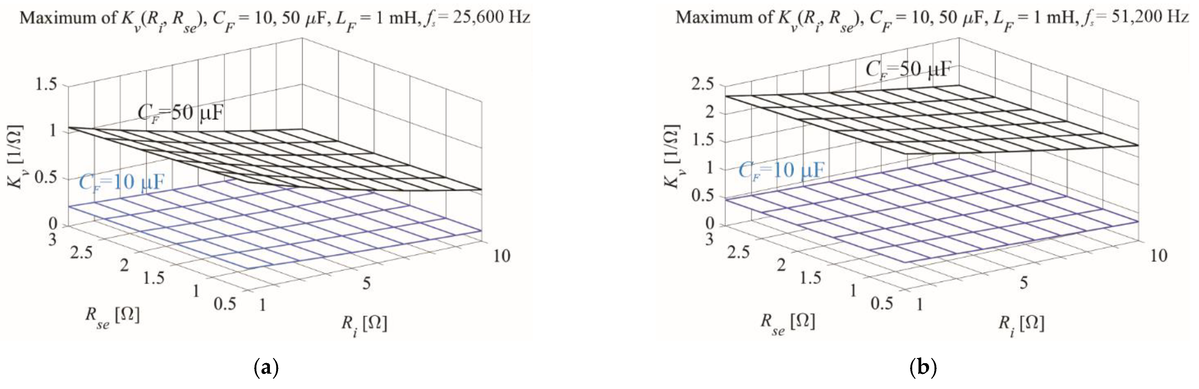
Equation (19) demonstrates the influence of switching frequency
fs = 1/
Ts and equivalent serial resistance
Rse on the maximum values of the IPBC2 gains. These relationships are portrayed in
Figure 2. The lower the value of
Ts/
LF, the lower the influence of the equivalent serial resistance
Rse. For high values of
fs, the influence of
Rse will be negligible, and the maximum voltage and current gains will be higher [
22]. This demonstrates the weak influence of equivalent serial resistance on maximum gains.
The presented gain values are derived from simulation models featuring a reference voltage amplitude of unity, a bridge supplied by VDC, and controller input signals from the inverter model output scaled by a factor of 1/VDC. Amplification of the voltage trace was adjusted for the real inverter such that for the nominal amplitude of the output voltage fundamental harmonic for a 50 Ω load, for the ADC range −4095–4095, provided a value of 3000 units. The 3000 output value was adjusted for the unity voltage scaling ratio. For the 50 Ω load resistance, which was assumed to be nominal, the amplification of the current trace was adjusted until the ADC provided a reading of 2000 units. This gave an output current scaling ratio of (3000/2000)/50 = 0.03. For a small output capacitance of 1 μF, it was performed the same adjustment procedure was performed for the inductor current trace, and the same current scaling ratio of 0.03 was obtained. The voltage and current scaling factors require careful adjustment because they are multiplied by the PBC controller gains. For the experimental inverter, reference amplitudes of 1640 and 820 for the 25,600 Hz and 51,200 Hz switching frequencies, respectively, were used. For each set of values, 3000 units were used for the voltage and 2000 units for the current as nominal ADC values. Therefore, the gain scaling factors between simulation and experiment were r(25,600 Hz) = 3000/1640 = 1.829, and r(51,200 Hz) = 3000/820 = 3.659 for 25,600 Hz and 51,200 Hz, respectively. The scaled gains were assigned as Riinverter = Risym/r and Kvinverter = Kvsym/r. The MISO-PBC system is robust against a decrease in serial equivalent resistance. As such, this paper presents no further research on the subject.
3. The Theoretical Influence of Equivalent Serial Resistance Influence on the SISO-CDM Control Loop
The design of the Manabe CDM [
23,
24,
25,
26] controller (
T,
S, and
R polynomials) requires the assumed values of the coefficients of the closed-loop characteristic equation. In the simplest case of the Manabe standard form, these coefficients are defined as functions of the time constant
τ of the closed-loop system. The output voltage of a closed-loop system is given by Equation (20):
where
S includes the additional loop delay
Ts measured from the Bode plots of the loop. The characteristic equation of a closed-loop system in Manabe standard form is given by Equation (21):
The VSI is initially modeled as an output
LFCF filter, and described by the state equations
The state equations are solved for a single
k-th switching period
Ts, for double edge 3-level PWM, with a switching-on time period
TONk. The dependence of
xk+1 on
TONk is described by linearized exponential function Equations (25)–(28) [
21]:
where
The gain of the VSI, with double edge PWM and a digital modulator inserting a switching period delay
Ts, is given by Equation (29):
where
In our system, the load current
IOUT was treated as an independent disturbance, although it can be treated as a state variable. For a system with a disturbance, the degrees of
R and
S are greater than or equal to
n − 1, where
n is the degree of
D. The second degree of
S and the third degree of
R were assumed because of the additional loop delay in Equation (30):
Equation (21) is Diophantine; to obtain equal
ri and
si coefficients for equal degrees of
z, the following equation should be solved with
r0 =
p0 = 1 Equation (31):
The coefficients
pi of Manabe standard form for a continuous system are required for the 6th degree of
P(
s). They are given by:
where
τ is the time constant of a closed-loop system. Satisfactory results were obtained for the control of the tested experimental model, with
τ = 8
Ts.
Using the zero-order hold method, let us define a discrete-time transfer function using the
c2
d MATLAB function with a discretization cycle
Ts = 1/25600 s [
14] (32):
Consider the case for which
τ = 8
Ts (Ts = 1/25600 s):
The final calculation enables
vOUT =
vREF to hold in the steady state if the following condition is met (33):
For our experimental model,
LF = 2 mH,
CF = 51 μF, and
Rse = 1 Ω was assumed. Using these values, and with
τ = 8
Ts, the solutions of Equation (31) are:
The coefficient
t0 can be adjusted individually. The resultant difference control law is:
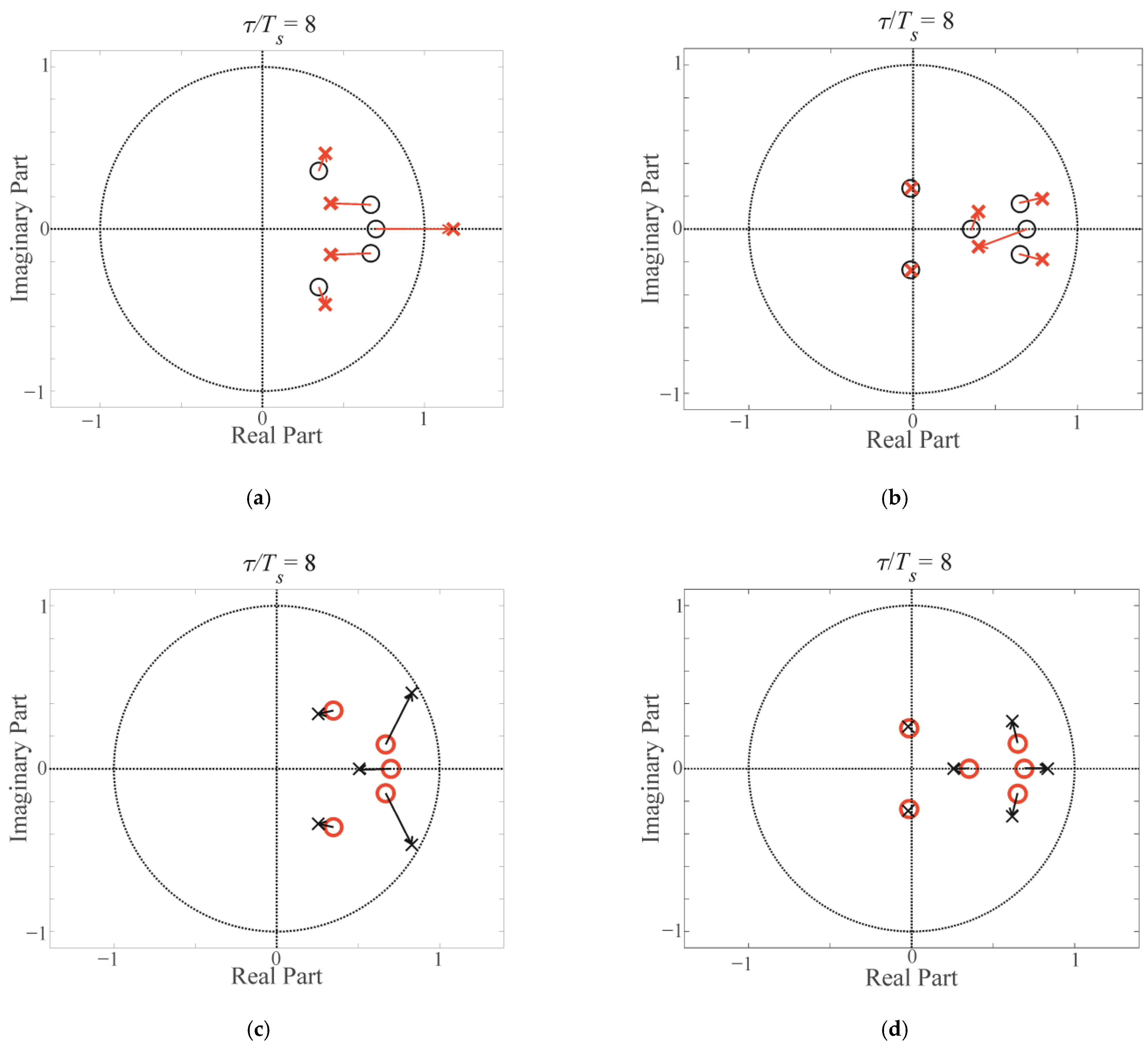
Figure 4 shows the shifts in the poles of the closed-loop CDM system (with
LF = 2 mH,
CF = 51 μF, and
τ = 8
Ts) caused by changes in
Rse.
Figure 4a,b shows a system that was configured for
RCDM =
Rse = 2 Ω, before
Rse was decreased to 0.4 Ω.
Figure 4c,d shows a system that was configured for
RCDM = 0.4 Ω, before
Rse resistance was increased to 2 Ω.
Figure 4a,c are for
S(
z−1) order 2,
R(
z−1) order 2,
Pz(
z−1) order 5, while
Figure 4b,d for
S(
z−1) order 2,
R(
z−1) order 3,
Pz(
z−1) order 6, which is required if the additional delay of the plant was taken into care. The examples presented in
Figure 4a,c show that for the lower order of the controller, SISO-CDM control is not robust to a decrease or increase in the equivalent serial resistance, and the system can be unstable, depending on the time constant τ.
Figure 4b,d shows that the system is more robust for the higher order of the controller for the same time constant τ. The SISO-CDM control was chosen for further investigation. The time constant of τ = 8
Ts was chosen because lower values caused small oscillations in the nonlinear rectifier RC for all types of transistors. It is difficult to analytically estimate changes in the dynamic properties of the inverter following the replacement of the transistors in the bridge, as the poles are shifted within the unity circle. As such, tests of the experimental model were conducted.
4. The Difference in the Static and Dynamic Equivalent Serial Resistance of the Same VSI When Using Si and WBG Switches
As shown in
Figure 5, the elementary VSI model is based on the output filter transfer function and the PWM modulator transfer function. The output filter transfer function is given by Equation (35):
where
A digital PWM modulator introduces a single switching period delay because the pulse width data that are calculated and stored during the current period will be in its output in the next switching period:
An additional delay can be introduced by double edge modulation [
27]. The sum of these delays is relevant for control system design if the switching frequency
fs is insufficiently high. However, as shown by Equations (4) and (11), the delay is compensated for during the relative measurement [
13] of the control transfer function of the bridge and filter
KCTRL, because a delay of period
nTs concerns both the fundamental harmonic and the excitation. As presented, the relative appointment of the magnitude and phase cancels this delay.
The equivalent serial resistance of the VSI [
25,
28] is measured using the resultant power conversion losses. The static and dynamic power losses in the switches and the filter coil core can be measured from the magnitude of a Bode plot of the inverter (operating with the assigned switching frequency
fs), within the range of frequencies where a maximum magnitude is located Equation (38):
Switching frequencies
fs of 12,800 Hz, 25,600 Hz, or 51,200 Hz were used for the test inverter. However, the frequency of the coil voltage pulses was double that of
fs in the first PWM scheme [
29]. The basic sinusoidal waveform had a fundamental frequency
fm = 50 Hz. The excitation sinusoidal waveforms had variable frequencies. The load resistance
RLOAD and the DC supply voltage
VDC were then set for the selected operating point. The generated test signal
VCTRL Equation (39) was the sum of the fundamental harmonic and the
n-th harmonic [
13,
28]. For
k = 1, …, (
fs/
fm),
where
M is the modulation depth (typically
M ≤ 1, e.g.,
M = 0.9 to avoid distortions of the fundamental harmonic),
fPWMINPUT is the microprocessor PWM unit comparator input frequency (84 MHz for the STM32F407VG), and
A is the relative amplitude of the fundamental harmonic (
A < 1, typically
A = 0.8–0.9 depending on the dumping).
In the case for which the switching frequency
fs =
nfm, there are
fs/50 samples of the sinusoidal reference during the fundamental period
Tm = 20 ms. From Equation (10), the number of samples of the
n-th harmonic during this period is
fs/(
n50). The value
nmax = 100 was used for both
fs = 25,600 Hz and
fs = 51,200 Hz to provide a minimum of five and 10 samples per harmonic period, respectively. The possible distortion of the
nmax harmonics was not important because of damping for harmonics above the output filter resonance frequency, which was adjusted below the 20th harmonic. Precise measurement of the magnitude of the harmonics was not required across the range of frequencies defined by the filter resonant frequency, where
ωF0 = 475 or
ωF0 = 498 Hz for the used filter coil inductance of
LF = 2 mH or 2.2 mH, although these values can vary by several percent [
28] for the coil core consisting of the low power loss materials Super MSS and FluxSan [
5]. An MKP
CF = 51 μF filter capacitor was used. The filter resonant frequency
ωF0, as defined by Equation (36), was calibrated to be much lower than 2π
nmax50 Hz.
The accuracy of the search for maximum gain was dependent on the frequency step grid. A low level of damping increases the error caused by the frequency step grid, causing difficulty in finding the exact maximum magnitude between the two measured points. However, a high level of damping can also cause ambiguity in the measurement of the maximum on the Bode plot. The LF and Rse parameters can be calculated directly only when the maximum of the damping coefficient can be found: ξF2 < (1 + Rse/RLOAD)/2, where RLOAD >> Rse. The measured fundamental harmonic amplitude should be equal to 50–75% of the ADC range. Given that a 13-bit bipolar ADC with a range of –4093–4093 units was used, the required amplitude was 2000–3000 units. The excitation amplitude |hnIN| = 1–A was set to the highest possible value (typically 10-20%) that did not cause the output voltage for the filter resonant frequency to exceed the range of the ADC.
The complex test signal
vCTRL, defined by Equation (39), has an amplitude of
floor(0.5
fPWMINPUT/
fs). A higher value of
fPWMINPUT corresponds to a more accurate synthesis of the control signal waveform by the STM32F407VG. A frequency
fPWMINPUT = 84 MHz is sufficient for
fs = 25,600 Hz. It was assumed that the fundamental harmonic is not damped within the inverter, and is delayed by
Ts or 2
Ts within the PWM modulator, as all components of the control signal are delayed. Hence, this delay is not present in the relevant calculations. Comparison of the output and input signals presents a problem, as the output voltage is measured in volts or ADC units, and the input control voltage is measured in PWM modulator comparator units. This problem is overcome by comparing the input and output excitations relative to the fundamental harmonics of the input and output, respectively. However, this approach is predicated upon the 50 Hz component not being damped. The amplitudes and phases of the harmonic components of the complex input and output signals are calculated using the fast Fourier transform [
25]. For
n = 1,…,
nmax,
The magnitude Bode plot is then
The phase Bode plot is not required for further calculations.
The measuring trace of the system influences the signal. As such, the trace characteristics (both magnitude and phase) were measured and subtracted from the corresponding initially measured data. The trace was subjected to negligible damping of less than 0.5 dB in the range of up to 500 Hz, with a phase shift corresponding to a delay of approximately 2
Ts. The corrected data of the control transfer function magnitude and phase were then plotted on a PC using MATLAB. The maximum values of the function |
KCTRL| and the frequency
ωmax for which |
KCTRL|
max = |
KCTRL(
ωmax)| can then be identified to calculate the damping coefficient
ζF Equation (43), and the serial equivalent resistance
Rse (44) [
25,
28]. The real value of
LF can also be measured; however, this is not necessary for our purposes. Under the assumption that
RLOAD >>
Rse,
ζF and
Rse can be calculated as follows Equations (43) and (44):
Using a 50 Hz grid (Δ
ω = 25 Hz), the frequency
ωmax can be approximated as Equation (45):
It was assumed that this approximation is the primary source of error in the calculation of
Rse. The error Equation (46) in the calculation of the damping coefficient
ξF is caused by the Δ
ωmax error associated with appointing
ωmax:
The error presented in Equations (47) and (48) is larger for low-load currents because such conditions hamper the determination of a maximum when compared to the two closest measured points. Typically, this error causes higher measured resistance for low-load currents. Another source of error when using a high-load current is a Bode plot magnitude with an insufficiently steep gradient. This makes determining the maximum difficulty. Equations (47) and (48) show that the error of the serial equivalent resistance measurement increases with the damping coefficient, and depends on the test signal frequency grid. As described by Equation (39), the lowest grid frequency used for the generation of the test signal was 50 Hz, which corresponded to Δω = 25 Hz.
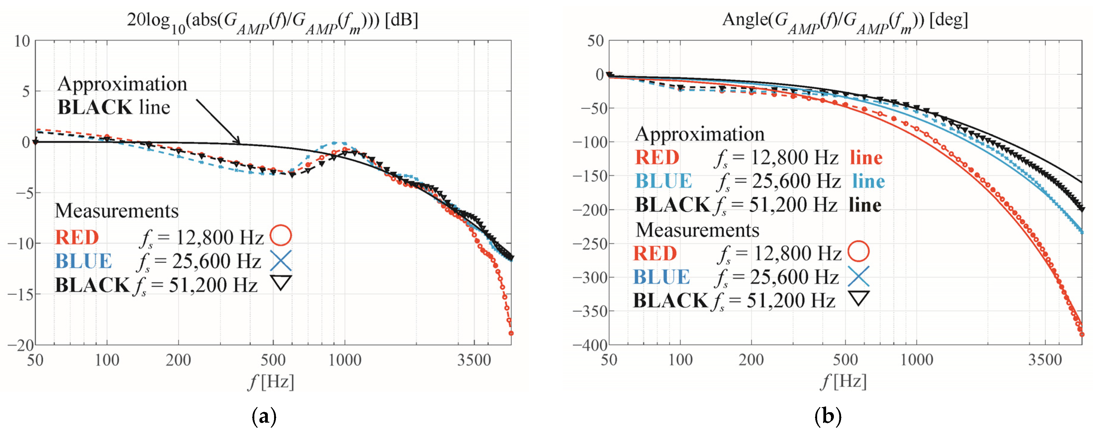
At the outset of the experiments, the magnitude and phase Bode plots of the experimental VSI were measured. A digital-to-analogue converter (DAC) was used to generate the test signal connected to the input of the measuring trace.
Figure 6 presents the magnitude and phase Bode plots
KTRACE(
s) of this trace, which can be approximated by the second-order transfer function with an additional 2
Ts delay:
The delay of the DAC is equivalent to that of the PWM modulator. As such, the pure trace has a delay of a single
Ts. The corner frequency of the output filter for
LF = 2 mH and
CF = 51 μF is 498 Hz, allowing
KTRACE Equation (50) to be approximated in the range up to 1000 Hz, using only the delay 2
Ts and omitting the second-order transfer function. All the measured signal traces are identical outside of the voltage and current inputs; these measurements are provided by the isolated amplifier and the AC current transducer, respectively. However, across the restricted frequency range, all traces are approximately identical.
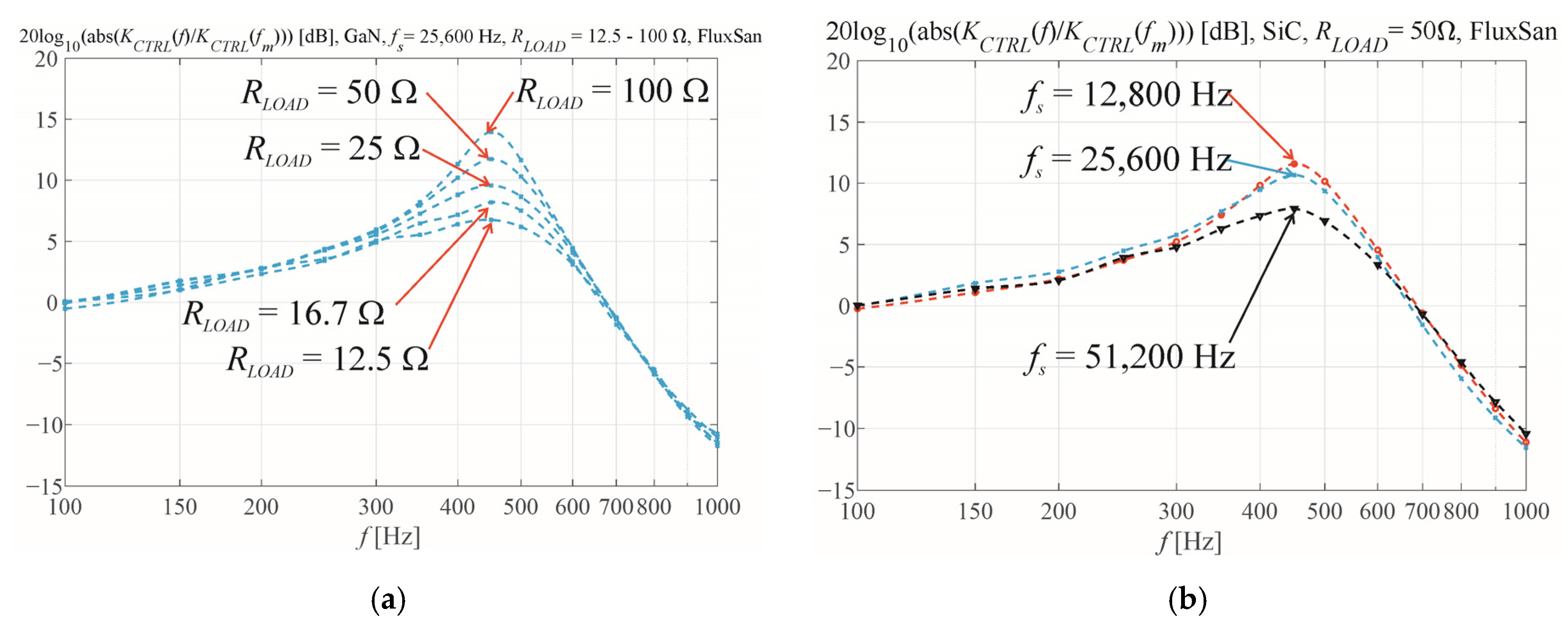
Three switching frequencies were implemented in the test system: 12,800 Hz, 25,600 Hz, and 51,200 Hz. Three types of transistors were used: the Si-based IRFP360, the SiC-based AIMW120R060M1H, and the GaN-based Cascode Device Structure GAN041-650WSB. Five resistive loads were used in the range of 12.5–100 Ω. This gave us a total of (transistors of 3 types) × (3 switching frequencies) × (5 load resistances) × (2 magnetic materials) = 90 different combinations of variables, and therefore 90 magnitude and phase Bode plots.
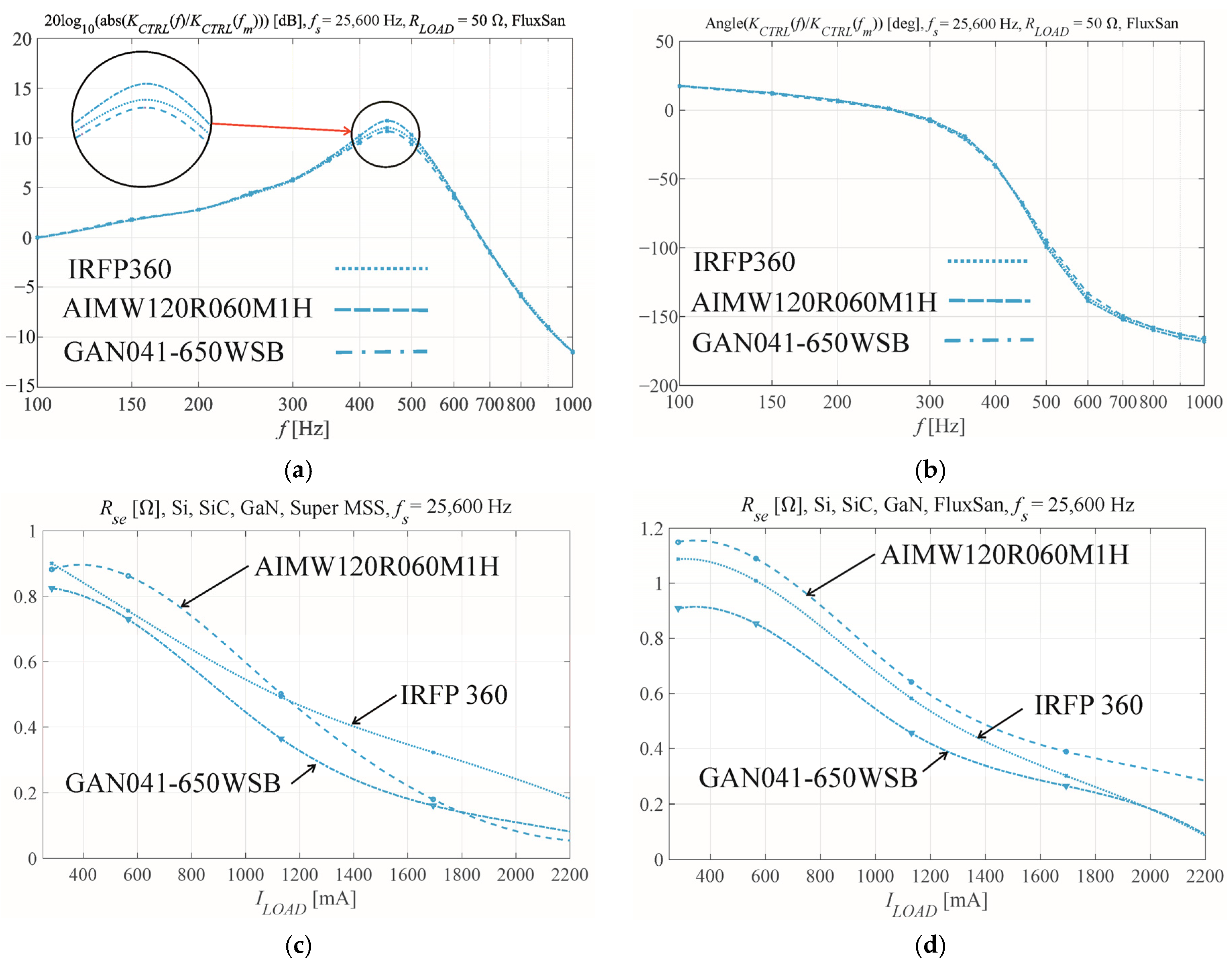
Figure 7 and
Figure 8 present selected examples of the Bode plots. The selection of the examples has to show the influence of the transistor technology on the inverter Bode plots (
Figure 7a,b) and finally on the dynamic serial resistances
Rse for the two coil core materials (
Figure 7c,d).
Figure 7a shows that the Si transistors have lower damping than the SiC transistors for
RLOAD = 50 Ω and a FluxSan coil core. The same result was observed for the Super MSS core. It was assumed that this was caused by higher power losses in the coil for faster SiC switches. The resultant equivalent resistances are shown in
Figure 7c,d for the Super MSS core and FluxSan core, respectively.
Figure 7 shows that the lowest equivalent serial resistance
Rse was obtained for GaN transistors. However, the differences between the three transistor types are small for the chosen switching frequencies when using the same coil core material and load current.
Figure 8a presents the exemplary influence of the load current on the magnitude Bode plot of the inverter with GaN transistors, and
Figure 8b shows the exemplary influence of the switching frequency.
Using Equations (43) and (44), the equivalent serial resistances can be calculated from the magnitude Bode plots as a function of the VSI inductor current. The inductor current is higher than the load current, and flows through the bridge switches. The accuracy of the calculations is limited by the resolution by which the maximum magnitude can be found. This is demonstrated in
Figure 8a; for the lowest load resistance of 12.5 Ω, the curve maximum is difficult to locate precisely via interpolation between the measured points. The amplitude of the test signal relative to the fundamental must be carefully selected.
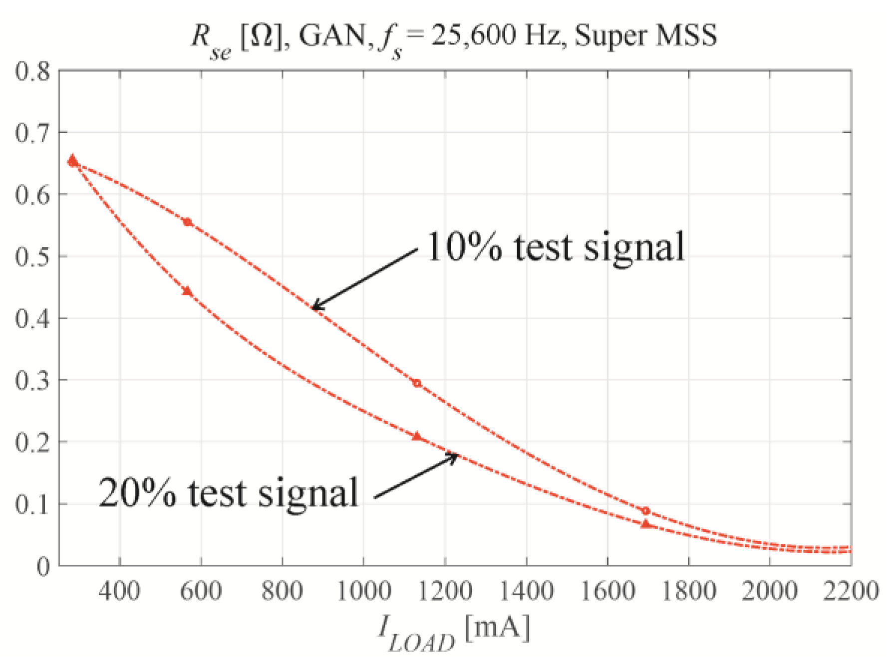
Figure 9 presents the serial equivalent resistance measurements for test signal amplitudes of 10% and 20% for
fs = 12,800 Hz, GaN transistors, and a Super MSS core. All presented calculations used a 10% test signal.
Measurement of the serial resistance
Rse is based on the invariability of the fundamental 50 Hz harmonic of both the input and output control trace signals. As such, static serial resistance was not measured. The efficiency of the experimental VSI was measured directly to calculate serial resistance
RLOSSES.
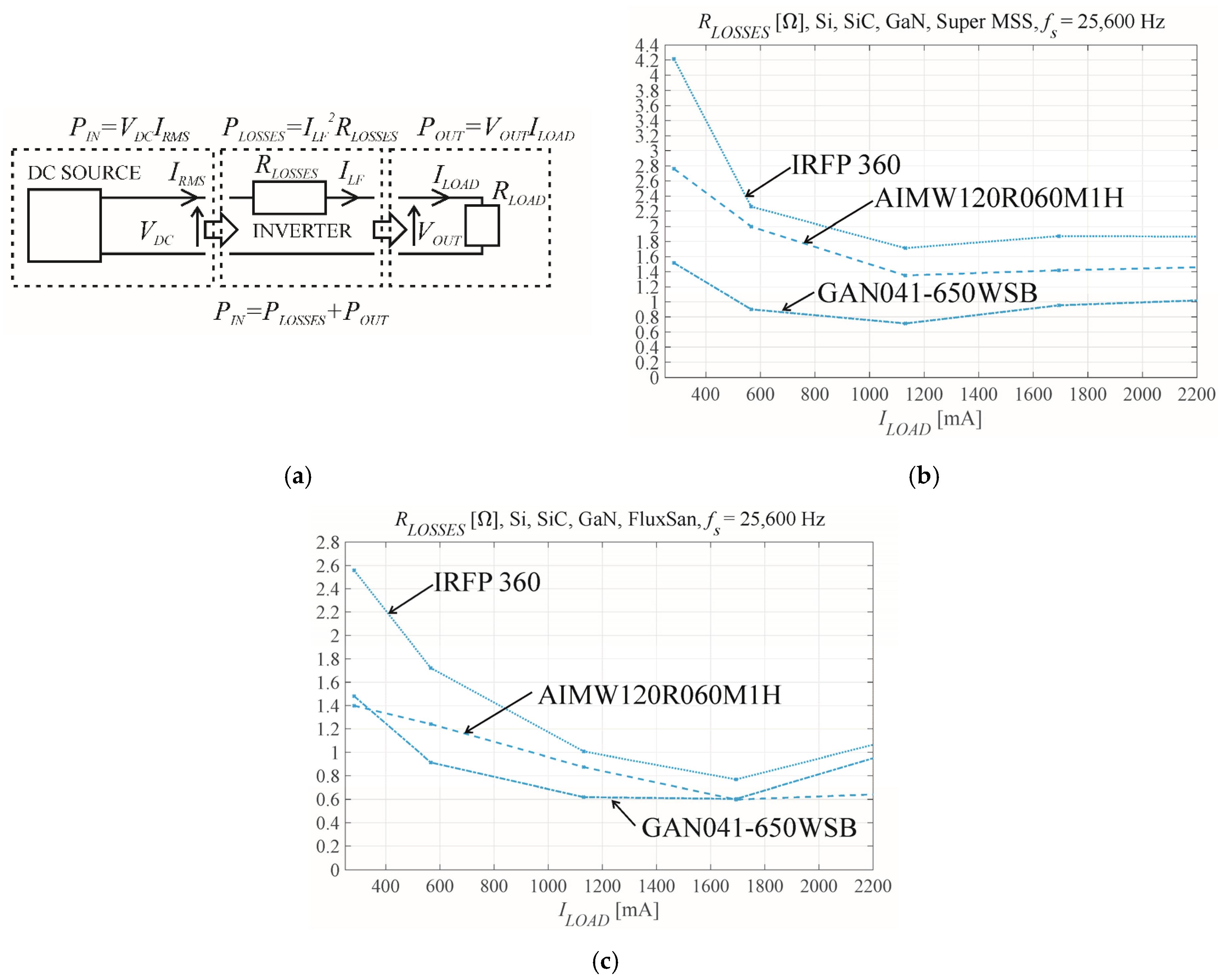
Figure 10 shows the exemplary measurements of
RLOSSES as a function of load current for both core types at
fs = 25,600 Hz. This resistance comprises the full losses from the DC source in addition to the dynamic losses and, as such, should be higher than the previously measured dynamic serial resistance
Rse of the control trace. It can be assumed that
RLOSSES =
R50Hz +
Rse, where
R50Hz represents the losses of the fundamental harmonic at 50 Hz in addition to the static losses.
Figure 11 and
Figure 12 show all the measurements of the serial resistances
Rse and
RLOSSES for the Super MSS and FluxSan core materials, respectively. The resistances were measured from the magnitude Bode plots or input and output powers for each transistor type. The dynamic serial resistance
Rse shows a slight dependence on transistor type at a given switching frequency and load current. However, the
Rse values are similar for both coil core materials. The full loss resistance
RLOSSES displays significant dependence on the transistor type, switching frequency, and type of coil core material.
The results of the two approaches to measure the equivalent serial resistance of the VSI are demonstrated in
Figure 11 and
Figure 12. The first is based on measuring the magnitude Bode plot of the control transfer function of the VSI (
Figure 5). This method is ideal for the estimation of the control loop parameters but has one disadvantage: it requires that the 50 Hz signal—the fundamental harmonic—is subjected to no damping. To correct the row measurements, the Bode plots of the measuring trace must be known (
Figure 6).
Figure 11 and
Figure 12 show that no substantial difference (less than 0.2 Ω) exists between the
Rse values of different transistor types at the same switching frequency when using the same coil core material. However, GaN-based transistors always produce the lowest
Rse.The complex equivalent resistance
RLOSSES can be calculated from the power losses of the VSI (
Figure 10). However, this resistance can include the component of the equivalent resistance that is outside the control loop and does not influence the quality of the output voltage. Both equivalent serial resistances
Rse and
RLOSSES depend on the type of transistor used (Si, SiC, and GaN), their static and dynamic losses, switching frequency, and the coil core material (Super MSS and FluxSan).
5. Tests of the VSI Using CDM Control for Different Switch Types and Coil Core Materials
The experimental VSI was used to validate the effect of implementing the correct equivalent resistance within the controller.
Figure 4b,d shows that for
fs = 25,600 Hz and a time constant
τ = 8
Ts, for the changes of the equivalent serial resistance, when the resistance
RCDM in the CDM control law is the same, the system is stable, but the poles of the closed loop system are shifted. For the lower time constant, measuring the unstable system (
Figure 4a) is impossible. It is possible to show that keeping the same resistance
RCDM in the control law for different transistor technology in the bridge for the same output filter coil core material can increase distortions of the output voltage. The idea behind the experimental verification of the previous theoretical considerations (
Section 3) is to find the resistance
RCDM in the SISO-CDM control law for which there are the lowest distortions of the output voltage and to show that it is connected with the equivalent serial resistance of the bridge (dependent on the type of switching transistors).
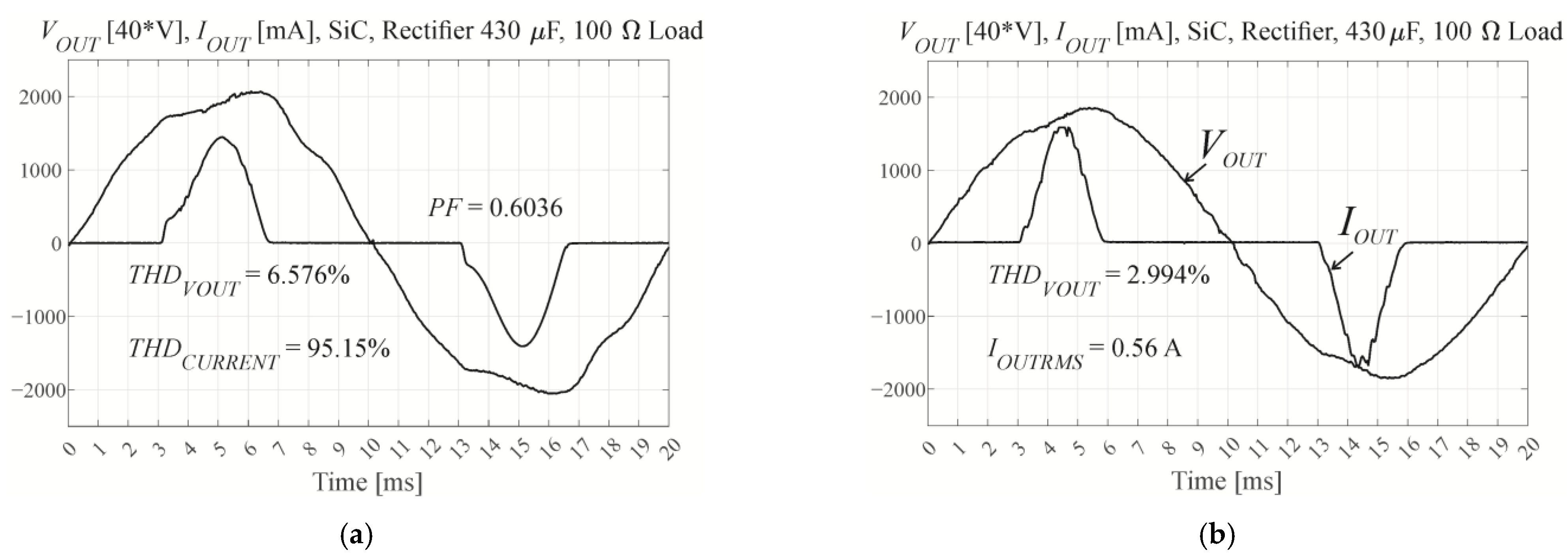
The various resistances
RCDM were used in the control law of the CDM controller for the different equivalent serial resistances of the VSI when using the nonlinear rectifier RC load defined in IEC 62040-3 (PF = 0.7) [
1]. The THD of the output voltages was measured for SiC transistors at
fs = 25,600 Hz using Super MSS coil core material, with both open-loop control and CDM control with
τ = 8
Ts.
Figure 13 shows the output voltage and current.
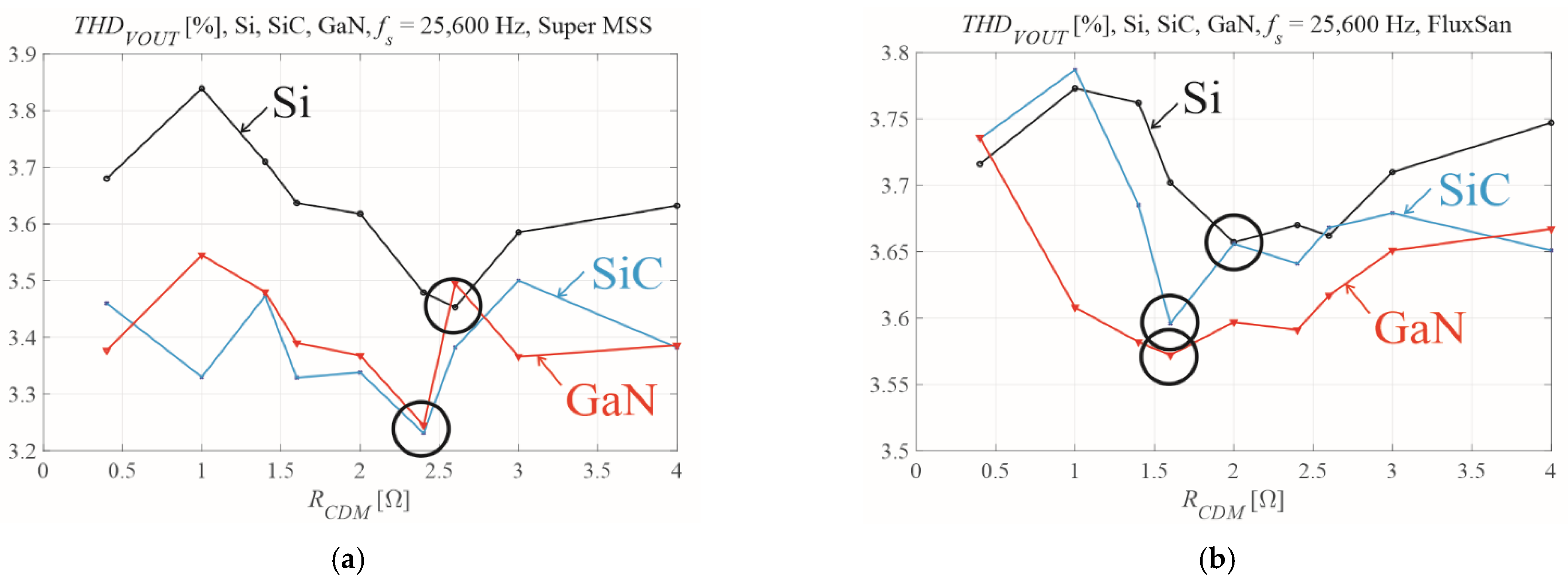
Figure 14 presents the
THDVOUT values for the different types of transistors and different sets of
RCDM resistances in the CDM control law. Both types of coil materials are shown with a switching frequency of
fs = 25,600 Hz and a time constant
τ = 8
Ts. The lowest
THDVOUT is obtained for the particular
RCDM that is comparable with
RLOSSES.
Table 2 presents the
RLOSSES resistances for
IOUTRMS ≈ 0.5 A at the
THDVOUT minima, for the Si, SiC, and GaN transistors, and the Super MSS and FluxSan core materials.
Figure 14 shows that for the high time constant when the system is stable, no matter whether the serial resistance in the control law is, the choice of the proper resistance
RCDM for the particular type of transistors and the coil core material improves the quality of the output voltage.
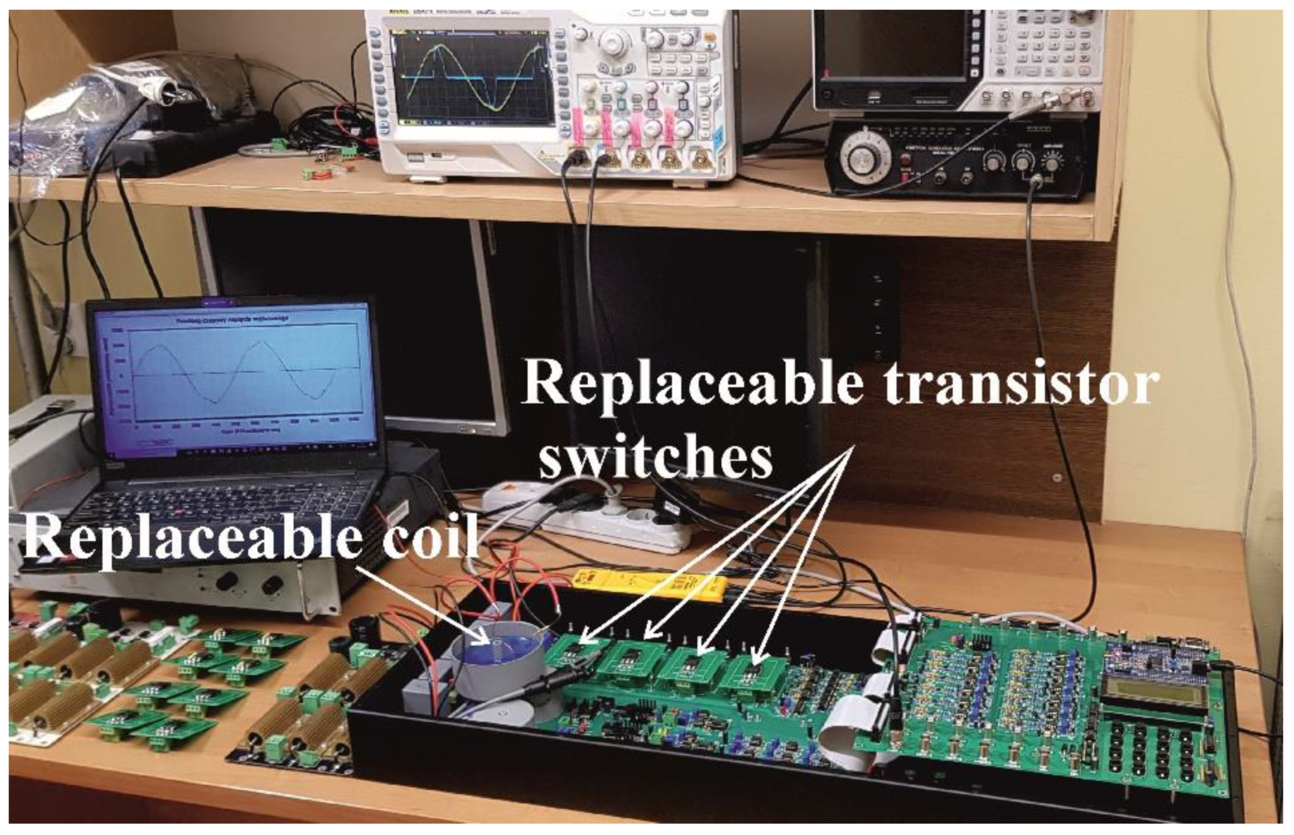
Figure 15 presents our experimental VSI setup for the measurement of Bode plots and
RLOSSES resistances.
When changing transistors, gate-driving circuits should be checked for oscillations. WBG transistors can oscillate due to associated parasitic elements. Switching oscillations can be damped using
RC snubbers, ferrite beads, a reduction in
di/
dt, or novel gate driver designs [
30]. Printed circuit boards (PCBs), which feature long traces between the gate driver output and the gate source terminal, can lead to high parasitic inductance in the gate loop and cause damage to SiC transistors [
31]. Moreover, SiC-MOSFETs are sensitive to parasitic components in the measurement probe. Measuring certain values (e.g., the gate-source voltage) can introduce parasitic inductance between the test point and the ground lead of the probe, thereby decreasing the stability of the SiC-MOSFET. However, if drain-source oscillations are noticed in a previously designed PCB, the simplest solution is often to increase the value of the serial resistor in the gate-driving circuit [
32].
Table 2 shows that the
RCDM resistance for which
THDVOUT was minimal was of comparable size to
RLOSSES and was higher than
Rse. The relative change in
THDVOUT for different values of
RCDM was small—between 5 and 10%. GaN and SiC transistors produce the
THDVOUT minimum at the same
RCDM resistance for both coil core materials. The Si transistors produce the
THDVOUT minimum at different
RCDM resistance. These results demonstrate that SiC and GaN transistors can be mutually replaced without requiring any change in control, but that the replacement of Si transistors requires the control value of
RCDM to be adjusted.


