
A Bi-Directional Dual-Input Dual-Output Converter for Voltage Balancer in Bipolar DC Microgrid

Abstract
:1. Introduction
- (1)
- The DIDO converter simultaneously performs voltage balancing and bidirectional power controls with dual inputs and outputs. Independent bidirectional power control and balancing control are realized under all load conditions.
- (2)
- Three types of modulation methods are performed. All three modulations can compensate for unbalanced power. Among the three types of modulation methods, the second modulation method reduces the current ripple in the voltage balancer without increasing the switching frequency.
- (3)
- To maintain voltage balancing without active input sources, additional modulation and control methods are required. Unlike conventional converters, this paper proposes a voltage balancer mode without active input sources.
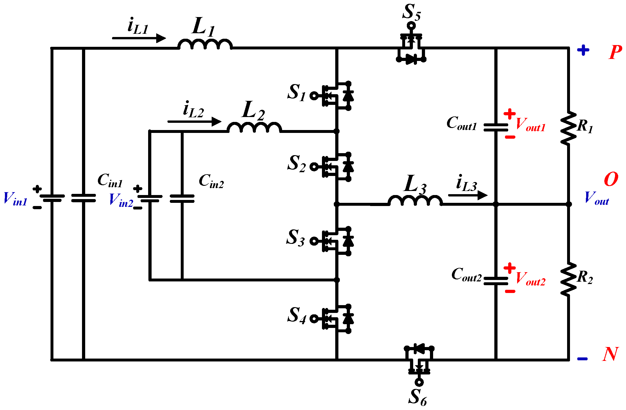
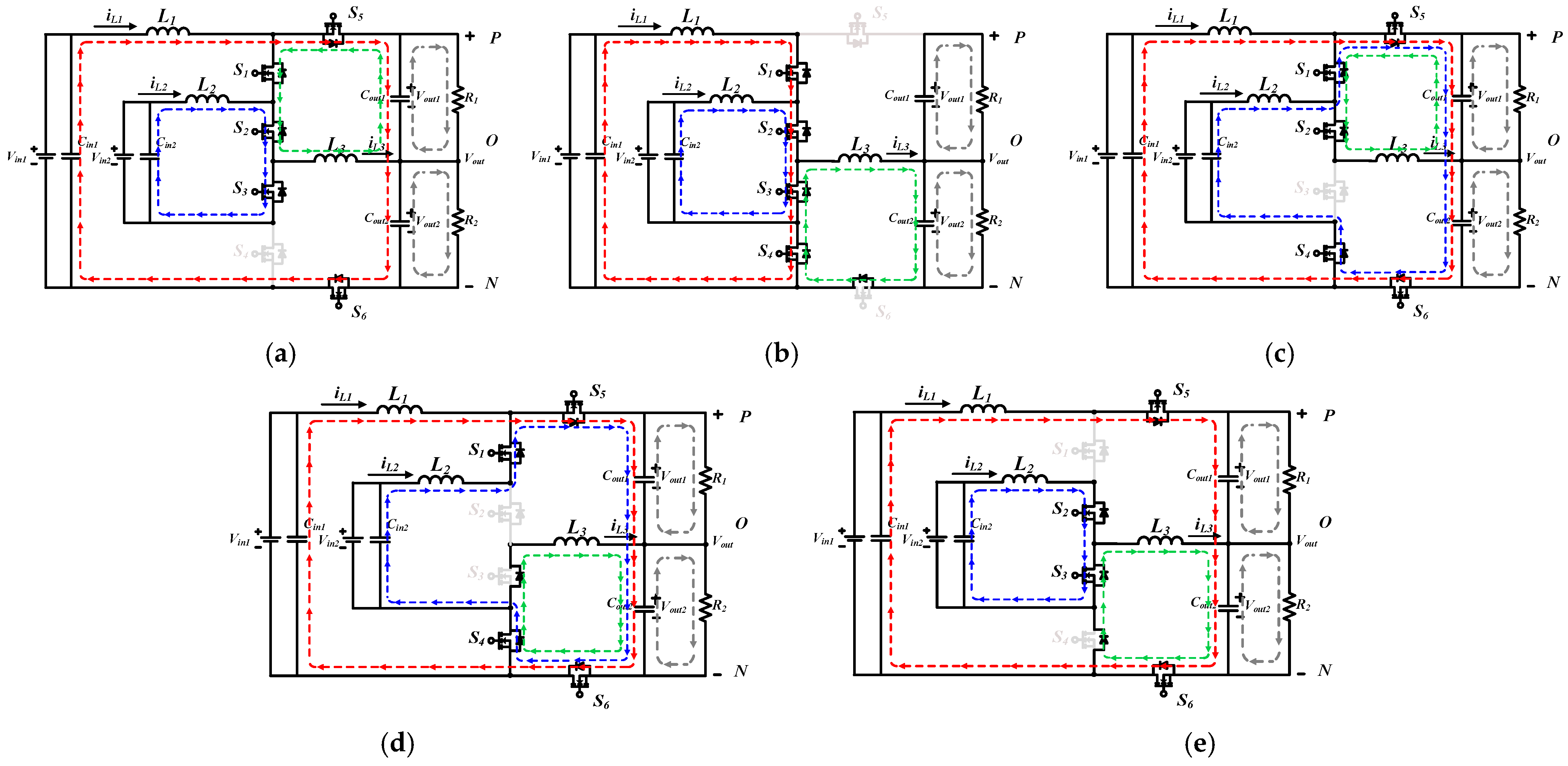
2. Proposed DIDO Converter
2.1. Configuration of the DIDO Converter
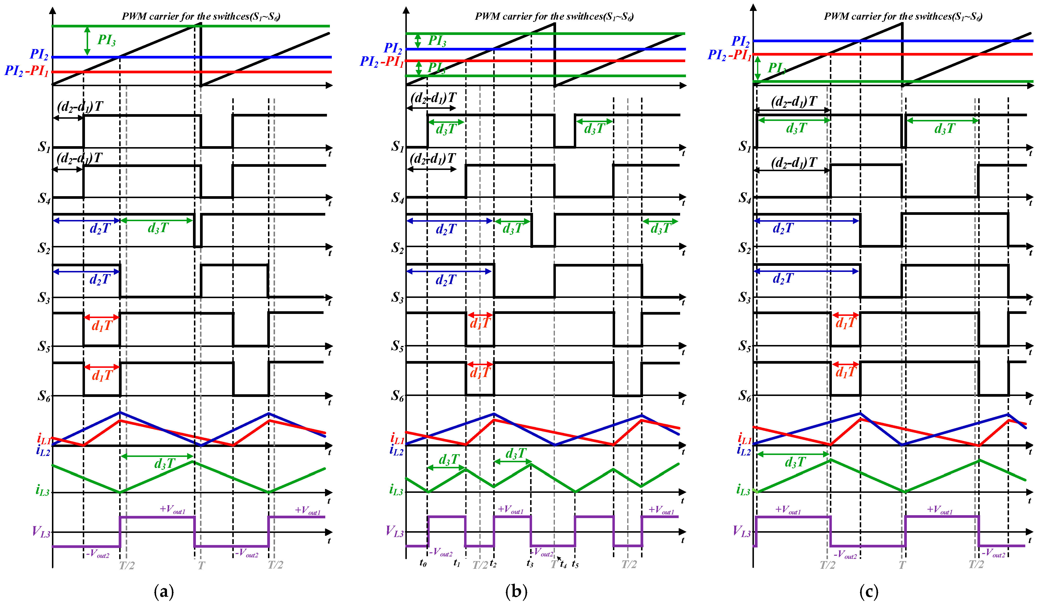
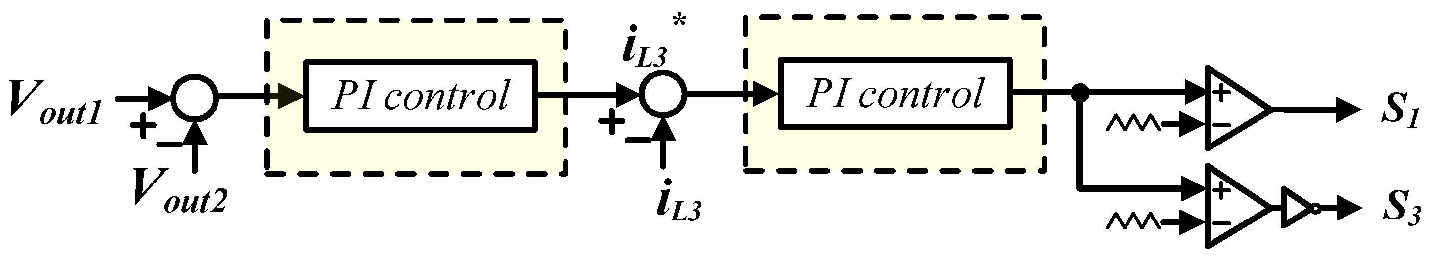
2.2. Modulation Methods of DIDO Converter for Voltage Balancing in BDCMG
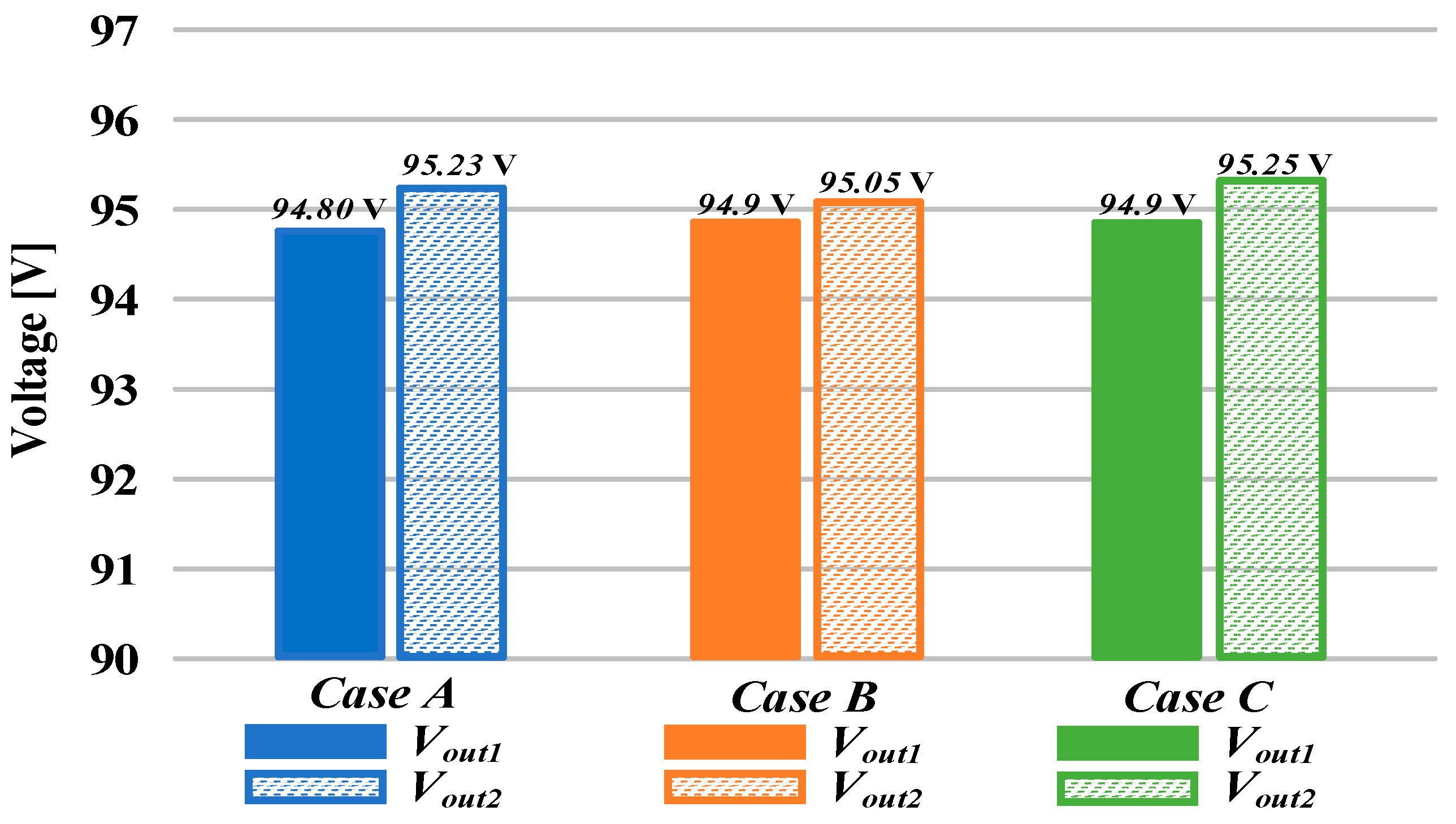
2.2.1. Case A:
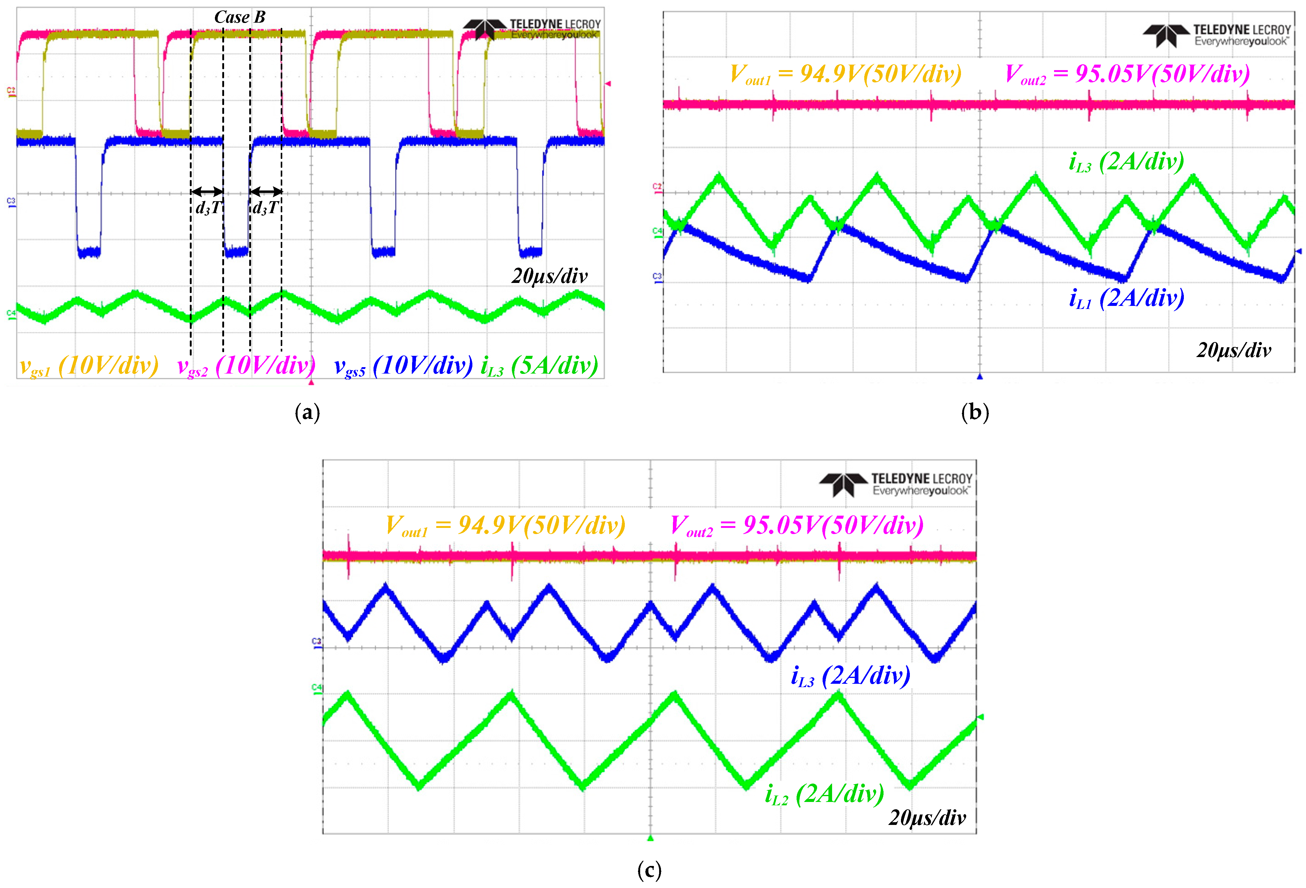
2.2.2. Case B: and
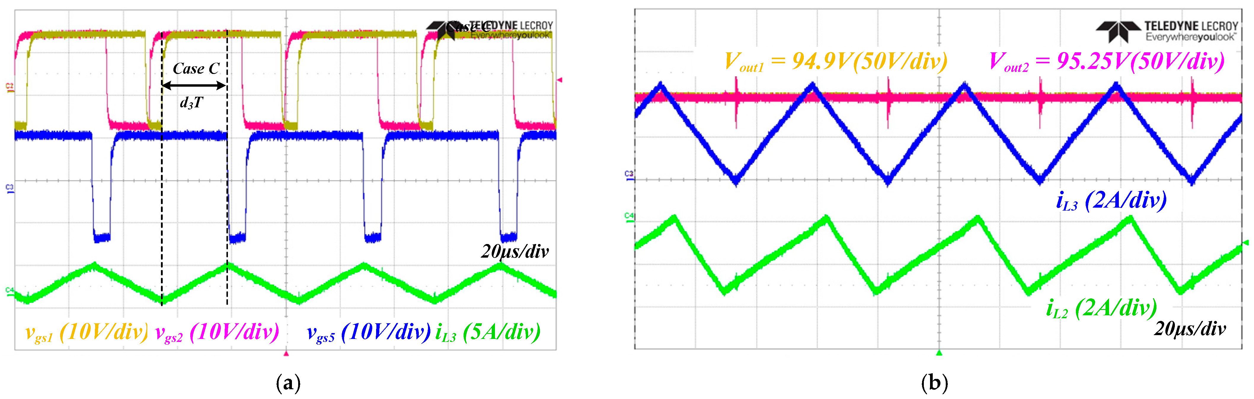
2.2.3. Case C:
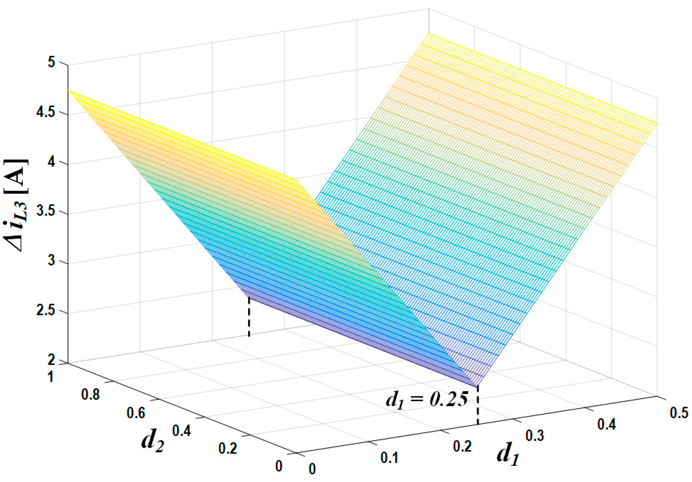

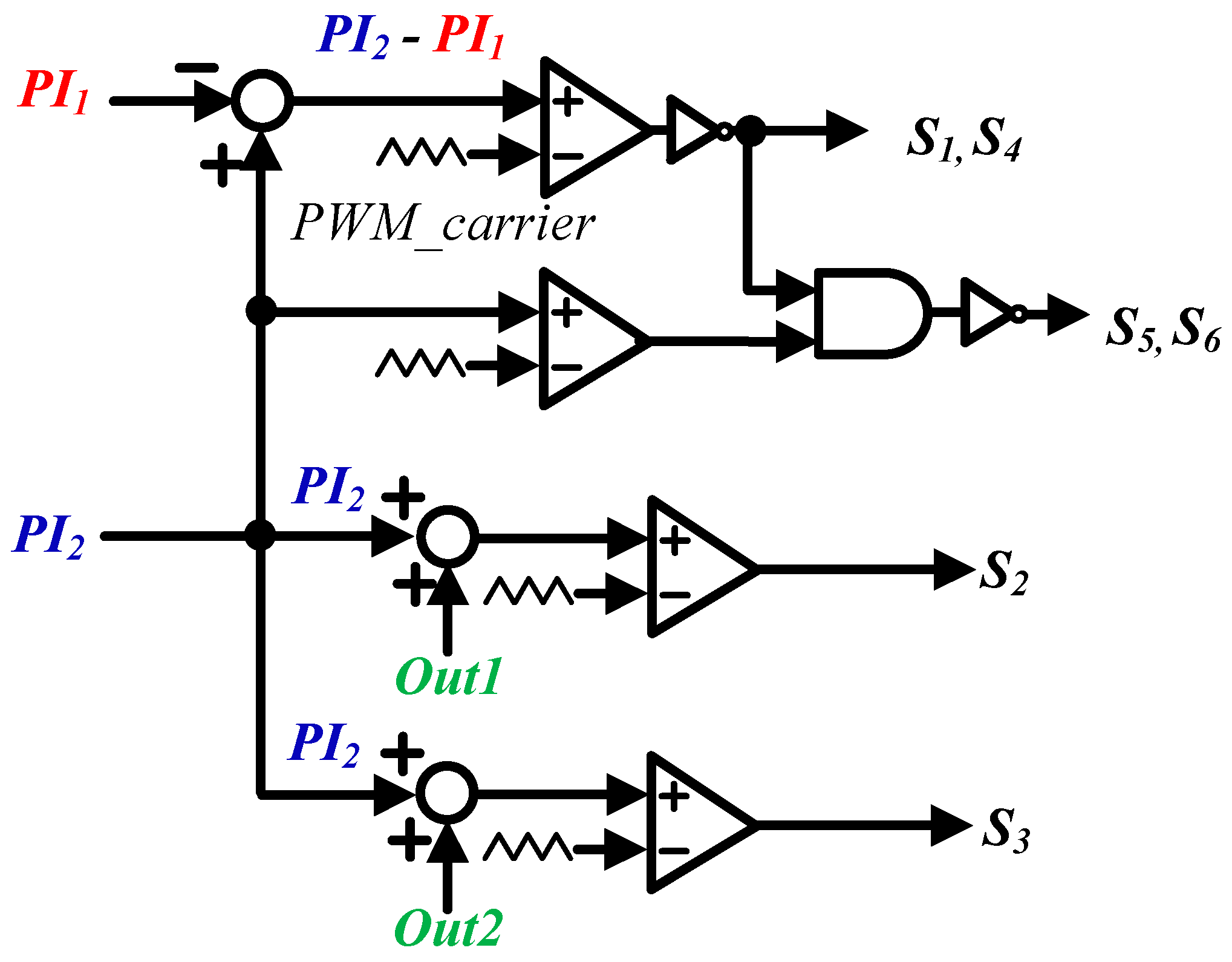
2.3. Modulation Methods of DIDO Converter for Voltage Balancing in BDCMG
2.4. Modeling of DIDO Converter
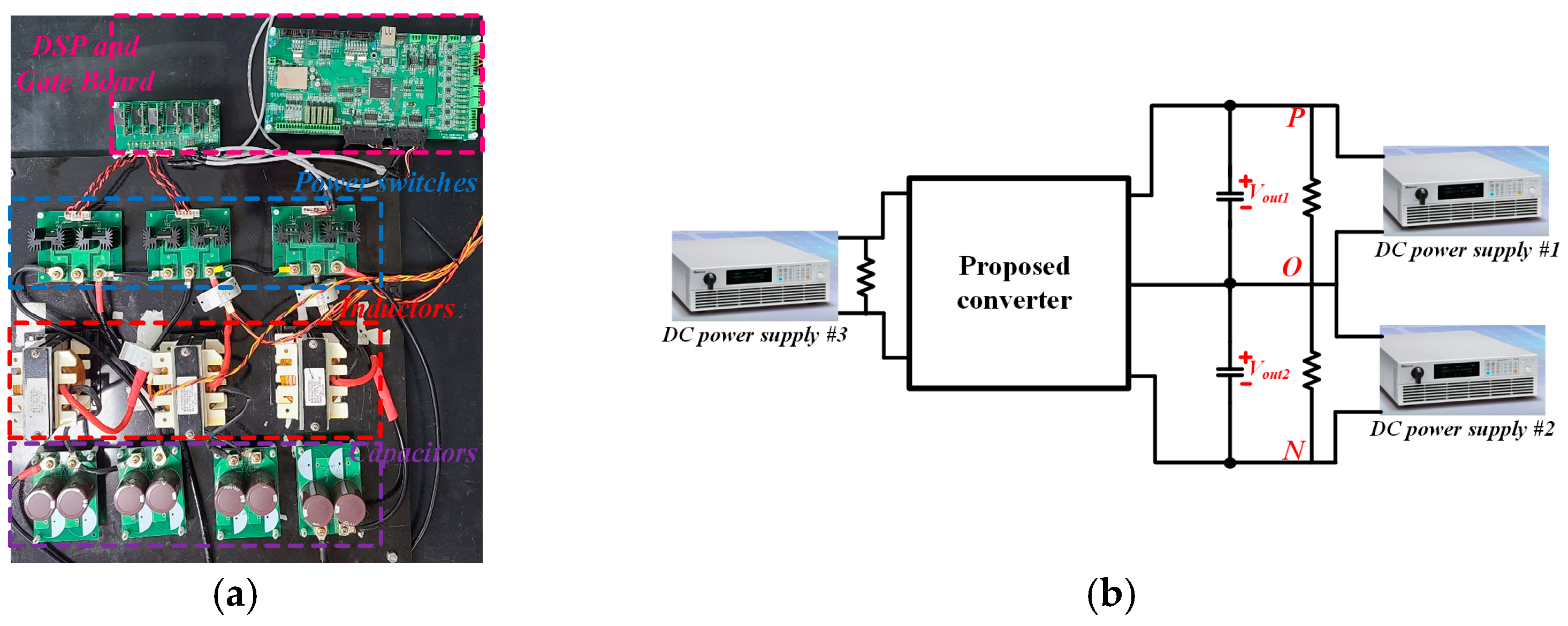
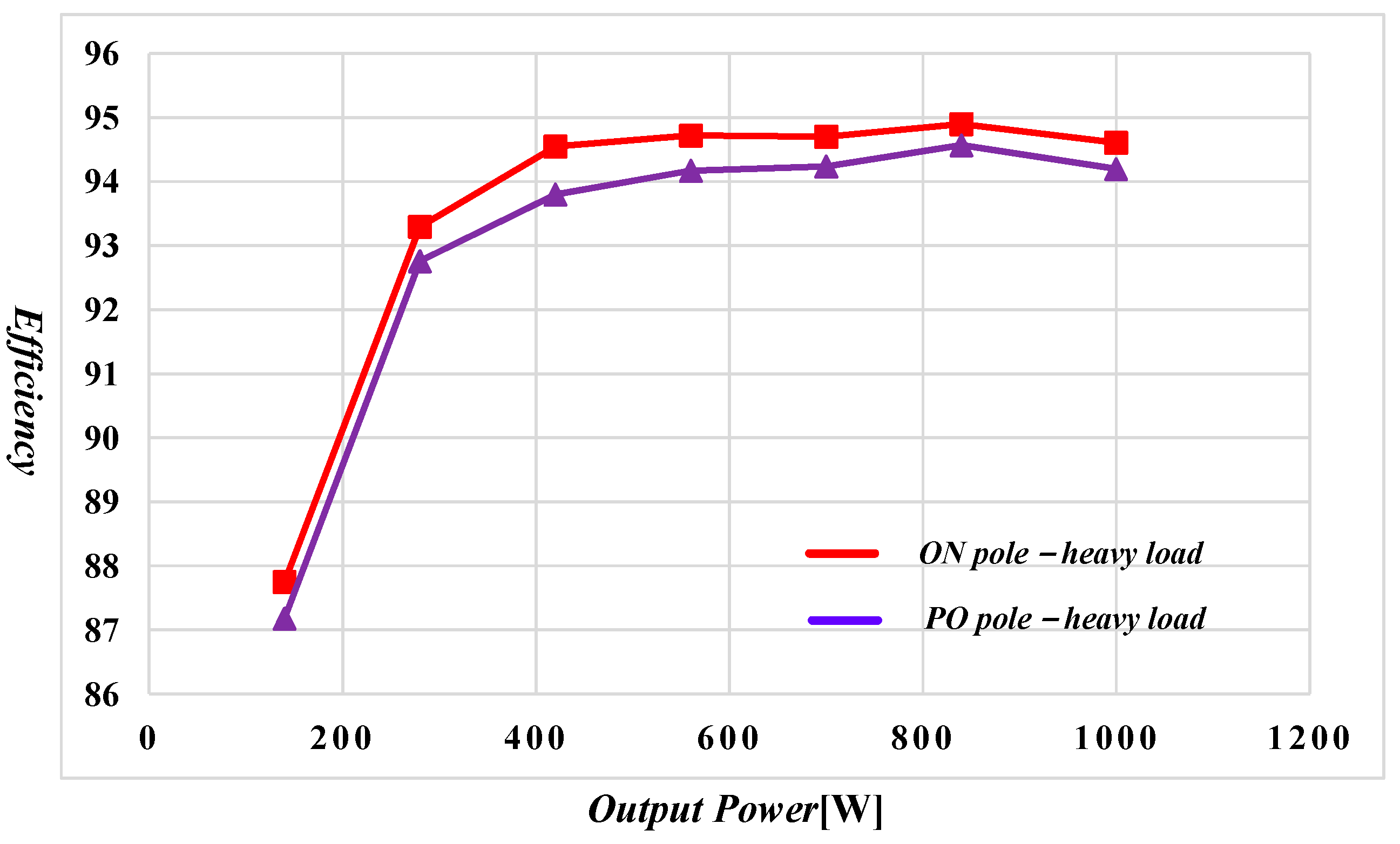
3. Experimental Results
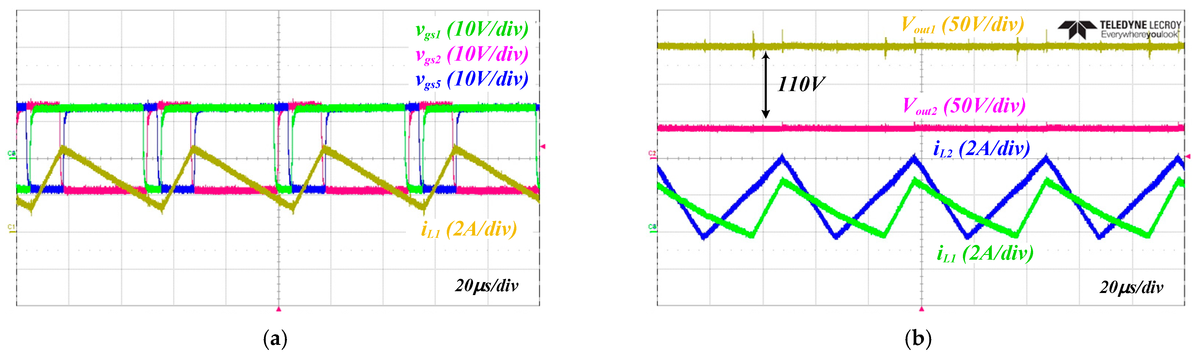
3.1. Experimental Result of the DIDO Converter without Voltage Balancing Method
3.2. Experimental Results with the Proposed Method in Case A
3.3. Experimental Results with the Proposed Method in Case B
3.4. Experimental Results with the Proposed Method in Case C
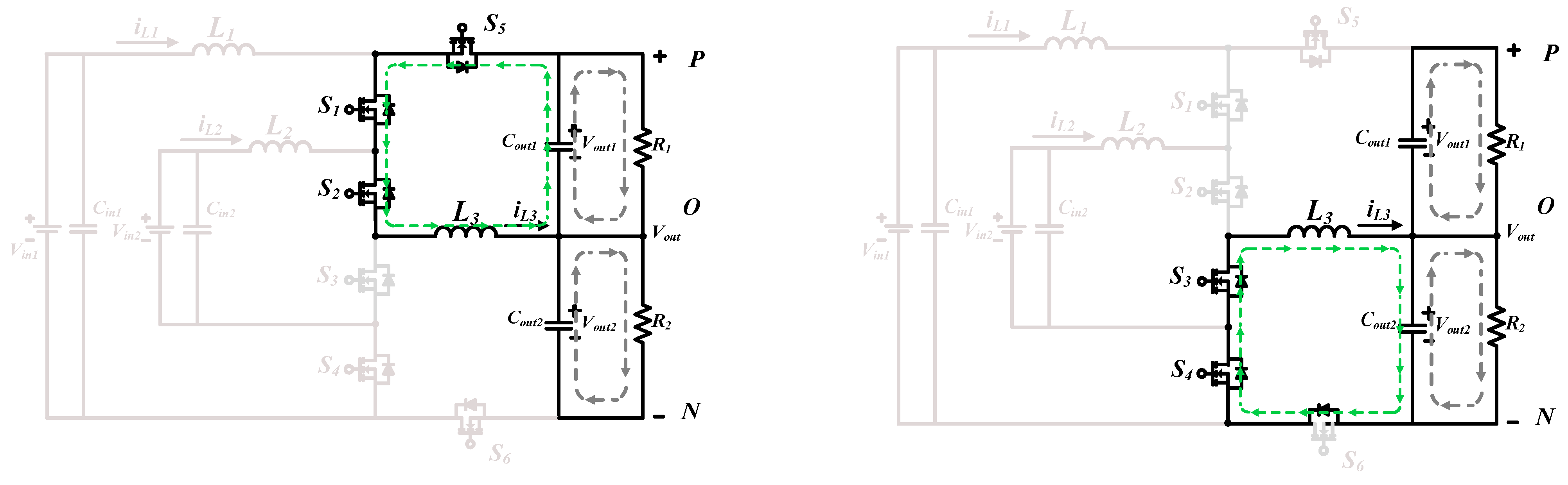
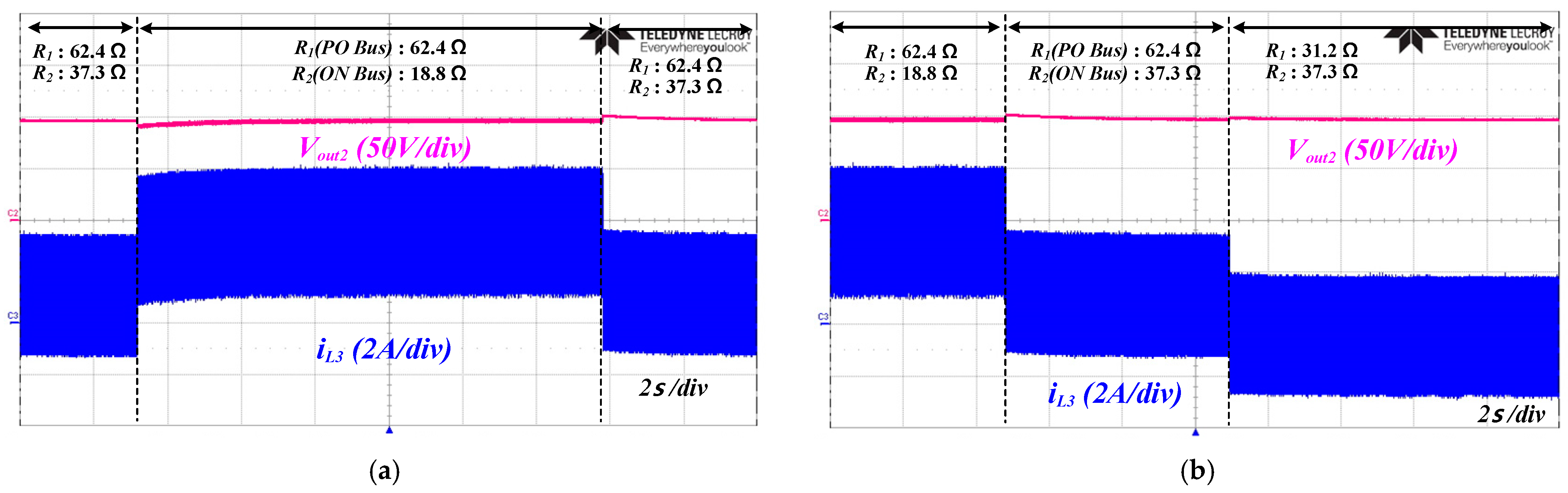
3.5. Experimental Result of the Only Voltage Balancer Mode
3.6. Comparison of Conventional Converters and the DIDO Converter in BDCMG
4. Conclusions
Author Contributions
Funding
Data Availability Statement
Acknowledgments
Conflicts of Interest
References
- Wang, P.; Goel, L.; Liu, X.; Choo, F.H. Harmonizing AC and DC: A hybrid AC/DC future grid solution. IEEE Power Energy Mag. 2013, 11, 76–83. [Google Scholar] [CrossRef]
- Dragičević, T.; Lu, X.; Vasquez, J.C.; Guerrero, J.M. DC microgrids—Part II: A review of power architectures, applications, and standardization issues. IEEE Trans. Power Electron. 2015, 31, 3528–3549. [Google Scholar] [CrossRef] [Green Version]
- Guerrero, J.M.; Vasquez, J.C.; Matas, J.; de Vicuna, L.G.; Castilla, M. Hierarchical control of droop-controlled AC and DC microgrids—A general approach toward standardization. IEEE Trans. Ind. Electron. 2010, 58, 158–172. [Google Scholar] [CrossRef]
- Wang, P.; Lu, X.; Yang, X.; Wang, W.; Xu, D. An improved distributed secondary control method for DC microgrids with enhanced dynamic current sharing performance. IEEE Trans. Power Electron. 2015, 31, 6658–6673. [Google Scholar] [CrossRef]
- Lu, X.; Guerrero, J.M.; Sun, K.; Vasquez, J.C. An improved droop control method for dc microgrids based on low bandwidth communication with dc bus voltage restoration and enhanced current sharing accuracy. IEEE Trans. Power Electron. 2013, 29, 1800–1812. [Google Scholar] [CrossRef] [Green Version]
- Kakigano, H.; Miura, Y.; Ise, T. Low-voltage bipolar-type DC microgrid for super high quality distribution. IEEE Trans. Power Electron. 2010, 25, 3066–3075. [Google Scholar] [CrossRef]
- Rodriguez-Diaz, E.; Chen, F.; Vasquez, J.C.; Guerrero, J.M.; Burgos, R.; Boroyevich, D. Voltage-level selection of future two-level LVdc distribution grids: A compromise between grid compatibiliy, safety, and efficiency. IEEE Electrif. Mag. 2016, 4, 20–28. [Google Scholar] [CrossRef] [Green Version]
- Zhang, X.; Gong, C. Dual-buck half-bridge voltage balancer. IEEE Trans. Ind. Electron. 2012, 60, 3157–3164. [Google Scholar] [CrossRef]
- Zhang, X.; Gong, C.; Yao, Z. Three-level DC converter for balancing DC 800-V voltage. IEEE Trans. Power Electron. 2014, 30, 3499–3507. [Google Scholar] [CrossRef]
- Wang, F.; Lei, Z.; Xu, X.; Shu, X. Topology deduction and analysis of voltage balancers for DC microgrid. IEEE J. Emerg. Sel. Top. Power Electron. 2016, 5, 672–680. [Google Scholar] [CrossRef]
- Ferrera, M.B.; Litrán, S.P.; Aranda, E.D.; Márquez, J.M.A. A converter for bipolar DC link based on SEPIC-Cuk combination. IEEE Trans. Power Electron. 2015, 30, 6483–6487. [Google Scholar] [CrossRef]
- Rezayi, S.; Iman-Eini, H.; Hamzeh, M.; Bacha, S.; Farzamkia, S. Dual-output DC/DC boost converter for bipolar DC microgrids. IET Renew. Power Gener. 2019, 13, 1402–1410. [Google Scholar] [CrossRef]
- Prabhakaran, P.; Agarwal, V. Novel boost-SEPIC type interleaved DC–DC converter for mitigation of voltage imbalance in a low-voltage bipolar DC microgrid. IEEE Trans. Ind. Electron. 2019, 67, 6494–6504. [Google Scholar] [CrossRef]
- Kim, S.; Cha, H.; Kim, H. High-efficiency voltage balancer having DC–DC converter function for EV charging station. IEEE J. Emerg. Sel. Top. Power Electron. 2019, 9, 812–821. [Google Scholar] [CrossRef]
- Broeck, G.V.d.; Martinez, W.; Vecchia, M.D.; Ravyts, S.; Driesen, J. Conversion efficiency of the buck three-level DC–DC converter in unbalanced bipolar DC microgrids. IEEE Trans. Power Electron. 2020, 35, 9306–9319. [Google Scholar] [CrossRef]
- van den Broeck, G.; Beerten, J.; Vecchia, M.D.; Ravyts, S.; Driesen, J. Operation of the full-bridge three-level DC–DC converter in unbalanced bipolar DC microgrids. IET Power Electron. 2019, 12, 2256–2265. [Google Scholar] [CrossRef]
- Tavakoli, S.D.; Khajesalehi, J.; Hamzeh, M.; Sheshyekani, K. Decentralised voltage balancing in bipolar dc microgrids equipped with trans-z-source interlinking converter. IET Renew. Power Gener. 2016, 10, 703–712. [Google Scholar] [CrossRef]
- Lee, J.; Cho, Y.; Jung, J. Single-stage voltage balancer with high-frequency isolation for bipolar LVDC distribution system. IEEE Trans. Ind. Electron. 2019, 67, 3596–3606. [Google Scholar] [CrossRef]
- Lee, J.-Y.; Kim, H.-S.; Jung, J.-H. Enhanced dual-active-bridge DC–DC converter for balancing bipolar voltage level of DC distribution system. IEEE Trans. Ind. Electron. 2019, 67, 10399–10409. [Google Scholar] [CrossRef]
- Prabhakaran, P.; Agarwal, V. Novel four-port DC–DC converter for interfacing solar PV–fuel cell hybrid sources with low-voltage bipolar DC microgrids. IEEE J. Emerg. Sel. Top. Power Electron. 2018, 8, 1330–1340. [Google Scholar] [CrossRef]


| Ref | Topology | Input Sources of Converter | Control and Voltage Balancing Method | Voltage Balancing without Input Source |
|---|---|---|---|---|
| [11] | SEPIC-Cuk Combination Converter | Single source | Unidirectional control with voltage balancing | No |
| [12] | Dual Output Boost Converter | Single source | Independent voltage control loops | No |
| [13] | Boost-SEPIC Interleaved Converter | Single source | Bidirectional control with voltage balancing | Yes |
| [14] | Modified Series-capacitor Converter | Single source | Bidirectional control with voltage balancing | No |
| [15] | Buck three-level Converter | Single source | Balancing control with modulation method | No |
| [16] | Full-bridge three-level Converter | Single source | Balancing control with modulation method | No |
| [17] | Integrated three-level Boost Converter | Single source | Independent voltage control loops | Not considered |
| [18] | Three-level DAB Converter | Single source | Balancing control with modulation method | No |
| [19] | Enhanced Two-level DAB Converter | Single source | Bidirectional control with voltage balancing | Not considered |
| [20] | DIDO Unidirectional DC–DC Converter | Dual sources | Unidirectional control with single bus voltage control | No |
| This paper | DIDO Bidirectional DC–DC Converter | Dual sources | 1. Bidirectional and voltage balancing control with modulation method 2. Only voltage balancer mode without input sources | Yes |
| - | Theoretical Analysis |
|---|---|
| Case | Operating Range of Duty Ratio | Used Switches for Voltage Balancing |
|---|---|---|
| A | S2 or S3 | |
| B | S1, S2 or S3, S4 | |
| C | S1 or S4 |
| Parameter | Value |
|---|---|
| Input voltage #1 (Vin1) | 150 – 170 V |
| Input voltage #2 (Vin2) | 55 – 130 V |
| DC link voltage (Vout) | 190 V |
| Inductor (L1, L2, L3) | 500 μH |
| Capacitor (Cin1, Cin2, Cout1, Cout2) | 280 μF |
| Switching frequency (fs) | 20 kHz |
| Topology | No. of Power Switches (MOSFET + Diode) | No. of Inductors + Capacitor (Input and Output) | Power Flow | Controllable Port (Input + Output Source) | Peak Efficiency (Power) |
|---|---|---|---|---|---|
| [11] | 1 + 2 | 4 + 5 | Unidirectional | 1 + 2 | 88.1% (450 W) |
| [12] | 2 + 2 | 2 + 3 | Unidirectional | 1 + 2 | 89.6% (53.5 W) |
| [13] | 4 + 0 | 3 + 4 | Bidirectional | 1 + 2 | 96.1% (200 W) |
| [14] | 4 + 0 | 2 + 3 | Bidirectional | 1 + 2 | 96.39% (60 kW) |
| [17] | 4 + 2 | 2 + 3 | Bidirectional | 1 + 2 | - |
| [20] | 2 + 4 | 1 + 4 | Unidirectional | 2 + 2 | 93% (200 W) |
| This paper | 6 + 0 | 3 + 4 | Bidirectional | 2 + 2 | 94.8% (1 kW) |
Publisher’s Note: MDPI stays neutral with regard to jurisdictional claims in published maps and institutional affiliations. |
© 2022 by the authors. Licensee MDPI, Basel, Switzerland. This article is an open access article distributed under the terms and conditions of the Creative Commons Attribution (CC BY) license (https://creativecommons.org/licenses/by/4.0/).
Share and Cite
Kim, S.-H.; Byun, H.-J.; Yi, J.; Won, C.-Y. A Bi-Directional Dual-Input Dual-Output Converter for Voltage Balancer in Bipolar DC Microgrid. Energies 2022, 15, 5043. https://doi.org/10.3390/en15145043
Kim S-H, Byun H-J, Yi J, Won C-Y. A Bi-Directional Dual-Input Dual-Output Converter for Voltage Balancer in Bipolar DC Microgrid. Energies. 2022; 15(14):5043. https://doi.org/10.3390/en15145043
Chicago/Turabian StyleKim, Sung-Hun, Hyung-Jun Byun, Junsin Yi, and Chung-Yuen Won. 2022. "A Bi-Directional Dual-Input Dual-Output Converter for Voltage Balancer in Bipolar DC Microgrid" Energies 15, no. 14: 5043. https://doi.org/10.3390/en15145043
APA StyleKim, S.-H., Byun, H.-J., Yi, J., & Won, C.-Y. (2022). A Bi-Directional Dual-Input Dual-Output Converter for Voltage Balancer in Bipolar DC Microgrid. Energies, 15(14), 5043. https://doi.org/10.3390/en15145043