Article

The Effect of a Metal Particle on Surface Charge Accumulation Behavior of Epoxy Insulator with Zoning Coating

School of Electrical and Information Engineering, Tianjin University, 92 Weijin Road, Tianjin 300072, China
*
Author to whom correspondence should be addressed.
Energies 2022, 15(13), 4730; https://doi.org/10.3390/en15134730
Submission received: 4 June 2022 / Revised: 22 June 2022 / Accepted: 24 June 2022 / Published: 28 June 2022

Abstract

:
Epoxy insulators are widely used in Gas-Insulated Transmission Lines (GILs), playing a significant role in electrical insulation and mechanical support. The metal particles generated during the production and operation of the equipment aggravate surface charge accumulation on the insulator, causing surface flashover. Therefore, it is necessary to study the suppression strategy of charge accumulation. In this paper, a downsized disc insulator was taken as the research object to investigate the effect of zoning coating on charge suppression with the presence of a linear aluminum metal particle under negative DC voltage. The zoning coating method was achieved by painting coatings with different conductivities in three areas on the insulator surface to regulate the charge. The inhibition mechanism of zoning coating on the charge accumulation in the presence of a linear metal particle was analyzed with the assistance of numerical simulation. The results showed that negative charges were accumulated in the nonplanar region as there was no metal particle, and the existence of metal particles led to the significant accumulation of positive charge speckles in the nonplanar region. The application of zoning coating could significantly inhibit the charge accumulation in the nonplanar area of the insulator and the charge injection from the grounded electrode to reduce the charge density. Under −25 kV, the maximum charge density on the insulator with the zoning coating was 48.1% lower than that without the coating, and the inhibition effect increased by 57.9% when the metal particle was introduced. This paper provides a new way to suppress the charge accumulation on the insulator surface.

1. Introduction

Traditional overhead lines, power cables, and other electrical equipment can be replaced by Gas-Insulated Transmission Lines (GILs). They are suitable for long-distance and high-capacity transmission and have great application potential [1]. Epoxy insulators are widely used in GILs. However, after a long time under a DC electric field, the free charge will be accumulated on the insulator surface. At present, it is generally believed that the surface charge is one of the important reasons to reduce the gas–solid interface insulation performance of the insulator. The electric field at the gas–solid interface will be distorted by the accumulated surface charge, which will cause surface flashover [2]. Therefore, it is necessary to study the charge accumulation mechanism in depth, and find effective strategies to inhibit the charge accumulation on the insulator.
Over the years, a large number of studies have been carried out to reveal the possible factors leading to charge accumulation, among which metal particles have been highly associated. During the production, transportation, installation, and long-term operation of equipment, metal particles are produced [3]. The particles near the insulator will not only directly distort the electric field on the insulator surface but also aggravate the accumulation of surface charges and cause serious harm to the electrical performance of insulators [4]. Linear metal particles have a more serious impact on the surface charge accumulation than metal particles of other shapes [5,6]. Due to the high electric field at the end of linear metal particles, micro-discharge is likely to occur and generate free charges. The charges are accumulated on the insulator surface under the application of the electric field. Gao, Y. et al. have studied the influence of bouncing linear metal particles on the charge accumulation of an epoxy insulator under DC voltage [7]. It has been pointed out that there are two main motion modes of the bouncing particle and the impact of a charged particle hitting the edge of the electrode on the charge accumulation is more significant than other modes. Wang, Z.Y. et al. studied the surface charge accumulation influenced by the adhering attitude of metal particles [8]. The study showed that the metal particles adhered to the insulator surface would cause a surge of surface charges, and the charge accumulation caused by the adhesion of metal particles along with the HV and grounded electrode was the most obvious. Li, B.T. et al. explored the influence of the length of the metal particle on the charge accumulation of the post insulator [9], where the lengths of the particle were 5, 10, and 15 mm respectively. It was revealed that an increase in the length could lead to obvious charge accumulation. As the length increased to 15 mm, negative charges were accumulated on the end of the particle. Cheng, H. et al. studied the surface charge distribution and electric field force of linear metal particle under DC voltage [10], and the effect of the electrode coating on the lift force of linear particles was discussed. It was shown that electrode coating could inhibit the charge accumulation by suppressing the initiation of particles.
Insulator surface treatment is one of the common methods to inhibit charge accumulation. In addition, surface coating can reduce the charge density by adjusting the surface conductivity of the insulator [11,12]. Gao, Y. et al. studied the effect of different contents of graphene oxide (GO) on the charge suppression performance of an epoxy/silicon carbide (SiC) coating [13]. Their conclusion showed that the epoxy/SiC coating had the best inhibition effect on the charge accumulation as the content of GO was 0.1 wt%. Deng, J.B. et al. discussed the charge accumulation on alumina-filled epoxy insulators covered with epoxy/SiC coating with different contents [14]. It was observed that the flashover voltage could increase when the content of SiC was 10 wt% to 20 wt%. However, if the content exceeded 50 wt%, the flashover voltage decreased due to the increase in surface leakage current. Du, B.X. et al. studied the surface flashover phenomenon by magnetron sputtering zinc oxide (ZnO) on the surface of the insulator to form a gradient coating with different surface conductivities [15]. It was shown that the surface flashover voltage of the coated insulator was improved. At present, scholars have preliminarily accepted the use of coatings doped with nanoparticles to adjust the charge distribution. However, most of them utilized a single type of coating, which may be not suitable for an insulator with a complex surface profile. In order to optimize the electric field distribution on the insulator surface, it is necessary to formulate the corresponding coating scheme for the specific shape of an insulator.
In this paper, a disc insulator and coaxial electrode system were designed. The charge accumulation behaviors of the insulator were studied and a zoning coating method to inhibit the charge accumulation on the insulator was proposed. The effect of zoning coating on the charge accumulation of the insulator with and without the metal particle under negative DC voltage was analyzed. The results showed that negative charges were mainly accumulated in the nonplanar region. As the metal particle adhered to the grounded electrode, positive charge speckles were accumulated in the nonplanar region. Zoning coating could significantly inhibit the charge accumulation and optimize the electric field distribution of the insulator surface.

2. Test Setup and Procedures

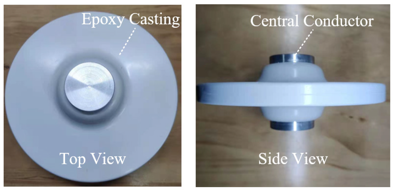
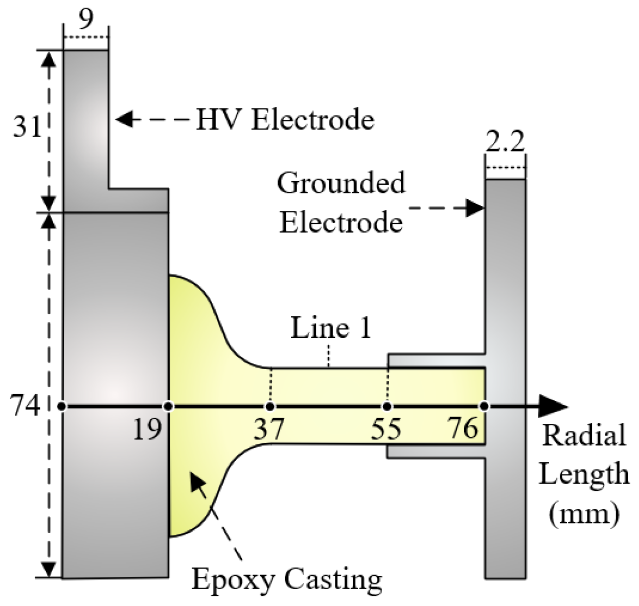
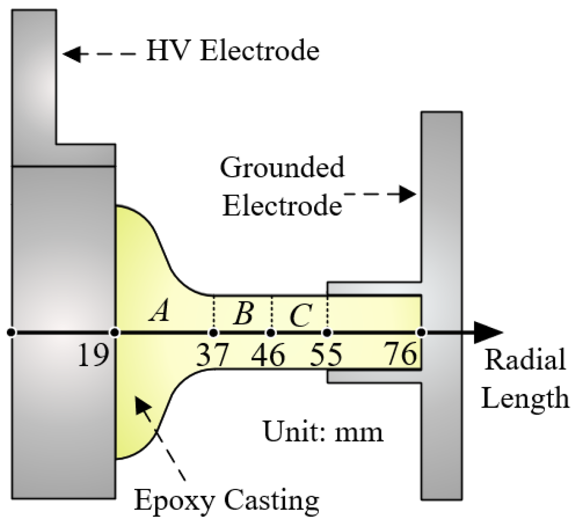
2.1. Test Insulator and Electrode Arrangement

The downsized disc insulator used in this paper was provided by Taikai Group Co., Ltd., Shandong, China. The insulator was cast by using epoxy and Al2O3 particles with a mass ratio of 1:3; the average size of the Al2O3 was 12–13 µm and its top view and side view are shown in Figure 1. In order to simulate the electric field distribution in a GIL, a coaxial electrode system was designed. The electrode system included an HV electrode and a grounded electrode. The HV electrode consisted of two parts; the upper part was used to connect the HV power supply, and its lower surface was in contact with the central electrode of the insulator. The field distribution was consistent with that in the real GIL, which was confirmed in our previous works [16,17]. The detailed dimensions of the insulator and electrode are shown in Figure 2. The area in line 1 is referred to as the planar region, and the rest is called the nonplanar region. The test insulator, along with the coaxial electrode, was placed in an enclosed test chamber in which the surface charge accumulation test was carried out.

2.2. Experimental Platform Arrangement

Before the experimental measurement, the test insulator was dried at 60 °C for 12 h to remove the moisture absorbed and was wiped on the surface with absolute ethanol. Then the potential of the sample was measured to ensure that there were no residual charges on the surface. In order to analyze the effect of gas ionization on the charge accumulation conveniently, the experiment was performed in air [16]. During the experiment, the chamber was sealed and the relative humidity in the chamber was controlled at 10 ± 2%. DC voltages of −15, −20, and −25 kV were applied and the insulator was charged for 1 h. Then, the HV power supply was disconnected, and the insulator surface was scanned with a Kelvin-type probe (3455ET) equipped with an electrostatic voltmeter (P0865). The probe was located 5 mm above the sample surface and was kept perpendicular to the surface during the measurement. In total, 648 potential data sets were sampled on the upper surface. The charge density was obtained by an inversion calculation [18,19].

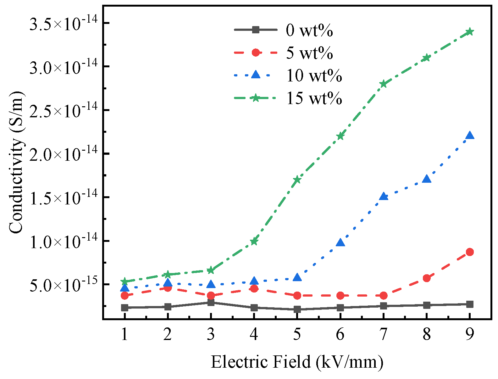
2.3. Preparation of Coatings with Different Conductivities

In this paper, the epoxy coating was based on the bisphenol-A epoxy resin (511#), which was produced by MACKLIN. The epoxy was a viscous liquid and the viscosity was 9000~14,000 MPa·s at 25 °C. The epoxy value was 0.48~0.54 mol/100 g. The curing agent was low-molecular-weight polyamide (651#), which was produced by MACKLIN. It was a brownish-yellow liquid and the viscosity was 2000~7000 MPa·s at 40 °C. The amine value of the polyamide was 380~420 mgKOH/g. The zoning coating method requires coating with different conductivities coated in different areas. In order to prepare coatings with different conductivities, different nanoparticles were added into the epoxy matrix. A high-conductivity coating was obtained by adding 4~20 nm graphene (GR) into epoxy. A low-conductivity coating was obtained by adding 30 nm Al2O3 into epoxy. A nonlinear conductivity coating was obtained by adding 40 nm SiC as filler. The epoxy-based nanocomposite coatings were prepared by the following procedure. The three kinds of nano particles were dried in a drying chamber at 100 °C for 12 h to remove the moisture. Then they were poured into the liquid epoxy according to the mass ratio. The mixture was put into the magnetic stirrer and ultrasonic cleaner for 1 h in each. The hardener was poured into the mixture with a mass ratio of 30:100 and the composite was treated under vacuum to evacuate the air. Finally, the treated coating was uniformly coated on the insulator surface and heated in the heating chamber at 70 °C for 3 h then 120 °C for 3 h to obtain the epoxy nanocomposite coatings. The reference sample was epoxy resin doped with micron-alumina fillers made by Taikai Group Co., Ltd., Shandong, China, which was made of the same material as the disc insulator used in the experiment.

3. Results and Discussion

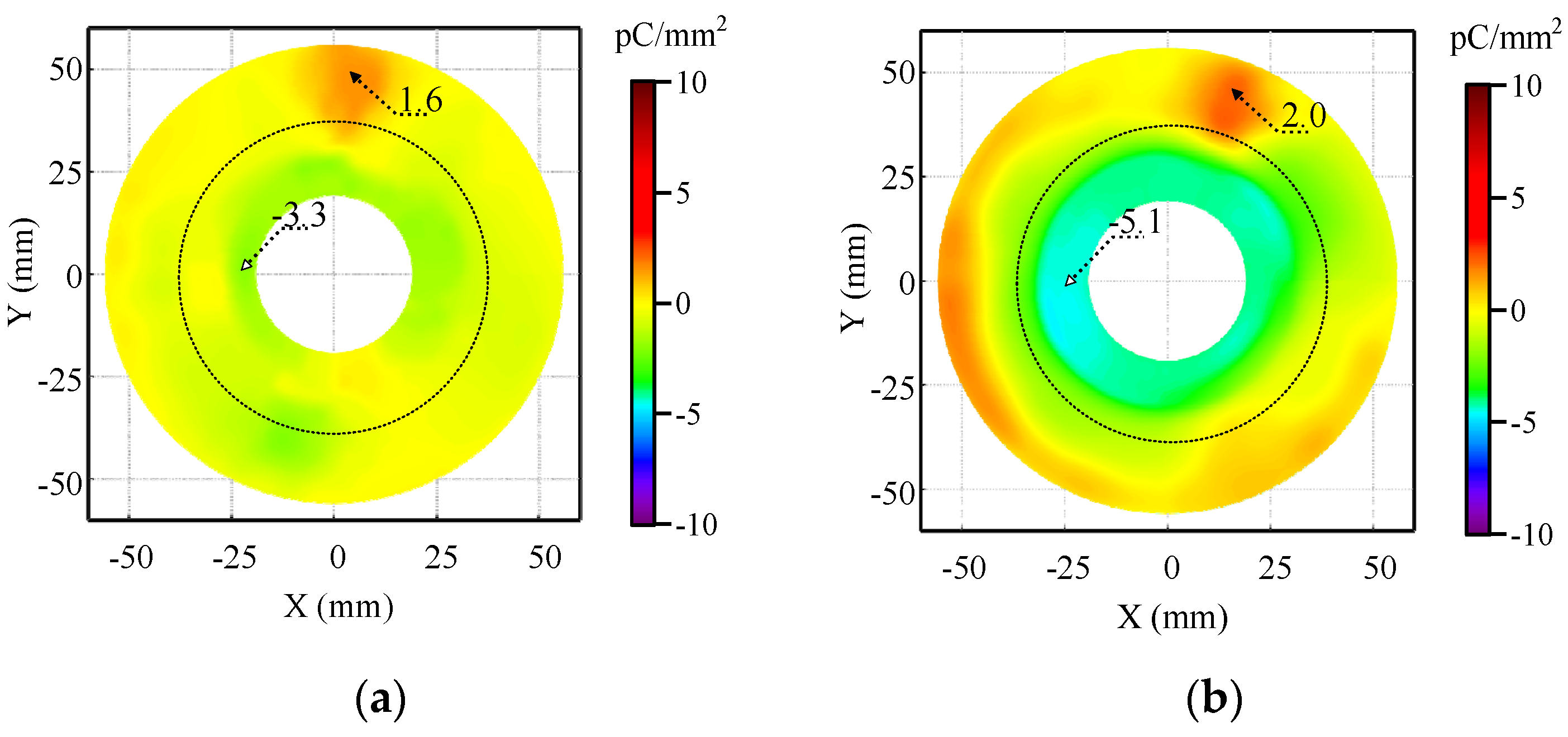
3.1. Behavior of the Charge Accumulation on the Insulator without Zoning Coating

The charge distribution of the insulator without zoning coating under −15, −20, and −25 kV is shown in Figure 3. The top view of the typical surface charge distribution is given. The inside of the dotted circle represents the nonplanar area, and the outside represents the planar area. In addition, the black triangle represents the maximum value of the charge density and the white triangle represents the minimum value. It is observed that positive charges with low charge density mainly accumulated in the planar region near the grounded electrode. With the increase in DC voltage from −15 to −25 kV, the maximum positive charge densities increased from 1.6 to 2.3 pC/mm2, which may have been caused by charge injection of the grounded electrode or micro-discharge [20]. However, the negative charges were mainly accumulated in the nonplanar area due to the injection by the HV electrode. With the increase in the DC voltage, the maximum negative charge densities showed a growing trend. The maximum values were −3.3 pC/mm2 under −15 kV, −5.1 pC/mm2 under −20 kV, and −8.1 pC/mm2 under −25 kV.
According to the experimental results, it is shown that negative charges were mainly accumulated in the nonplanar region whereas positive charges were deposited near the grounded electrode. Under the negative voltage, there was a strong normal component of the electric field in the nonplanar area, and the direction pointed to the insulator from the gas. Therefore, the negative charges injected by the insulator bulk and HV electrode were transported to the nonplanar region of the insulator surface under the electric field [16,17]. There was a strong tangential component of the electric field in the planar region. The direction pointed to the central conductor from the grounded electrode. Therefore, the positive charges injected by the grounded electrode were deposited near the grounded electrode.

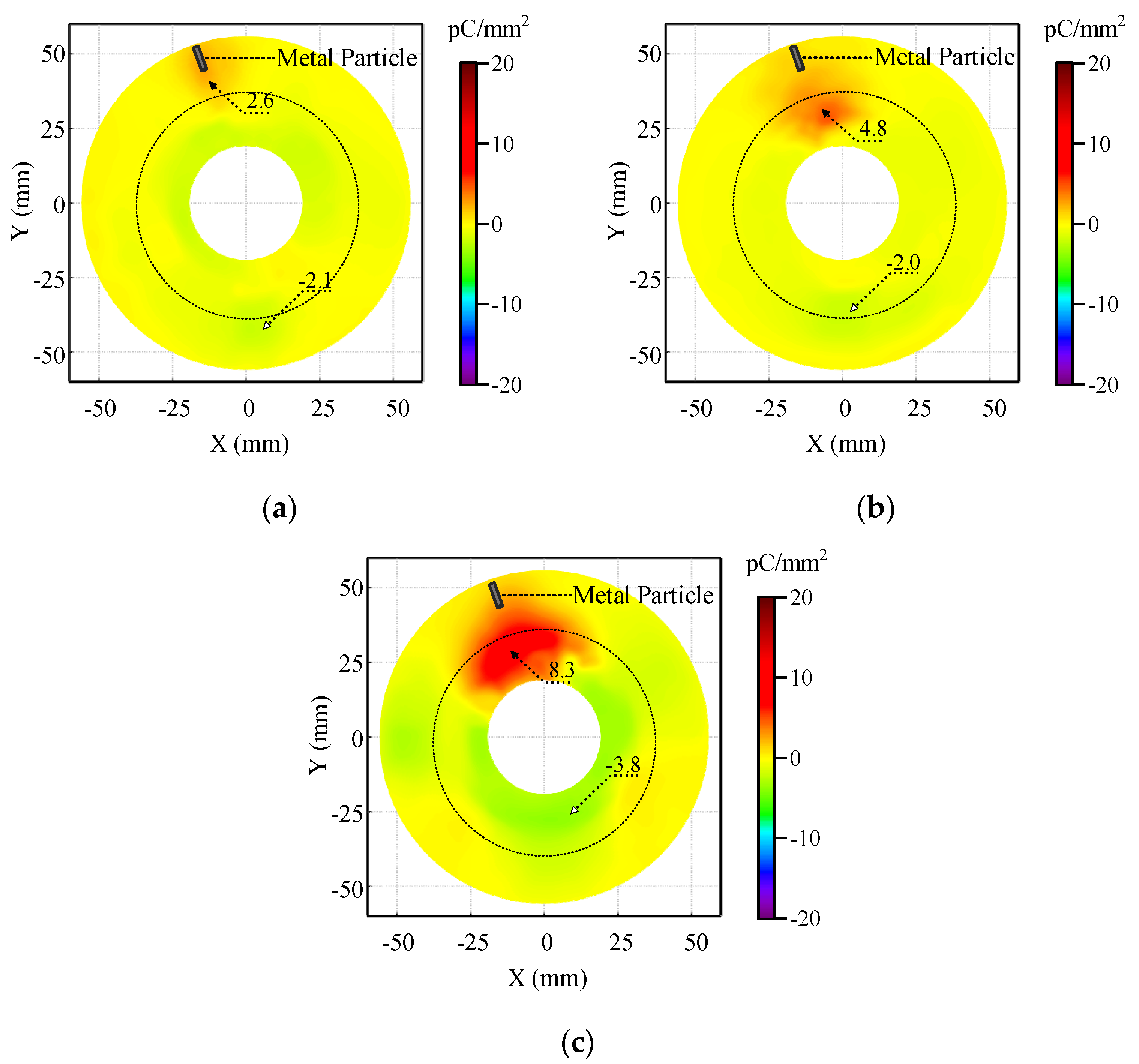
3.2. Behaviors of the Charge Accumulation on the Insulator with Zoning Coating

In this paper, a zoning coating strategy to inhibit charge accumulation is proposed. As shown in Figure 4, the insulator surface is divided into three areas, i.e., A, B, and C, where area A is in the nonplanar region and areas B and C are in the planar region. The high conductivity coating is painted in area A to accelerate the dissipation of the charges accumulated in the nonplanar area. The low conductivity coating is deposited in area C to inhibit the charge injection from the grounded electrode. The coating with nonlinear conductivity in area B plays a transition role between area A and area C. When the electric field increases, the conductivity of the coating in area B increases to accelerate the dissipation of the charges in area A.
Table 1 presents the surface and bulk conductivities of different coatings. As shown in Table 1, the surface conductivity of the sample with added 3 wt% Al2O3 is 1.27 × 10⁻¹⁹ S which is lower than the 1.3 × 10⁻¹⁸ S of the reference sample. The surface conductivity of the sample with added 3 wt% GR is 3.98 × 10⁻¹⁷ S which is higher than that of the reference sample. As shown in Figure 5, the conductivity of the sample with added SiC is a little higher than that of the reference sample. With the increase in the electric field, the conductivity of the sample begins to increase significantly when it reaches a certain value, showing the nonlinear conductivity characteristic. With the increase in the content of SiC, the electric field required for the nonlinear conductivity characteristic of the sample decreases. As the content of SiC increases to 10 wt% and 15 wt%, the epoxy/SiC coating presents the nonlinear conductivity characteristic under the high electric fields of both 5 kV/mm and 3 kV/mm. Nonlinear conductivity is a characteristic of SiC itself, so when the electric field increases to a certain value, the surface conductivity will increase with the field, just like the bulk conductivity. Therefore, the strategy of zoning coating is to apply a high-conductivity coating with 3 wt% GR in area A to promote charge dissipation, a nonlinear-conductivity coating with 15 wt% SiC in area B as a transition between areas A and C, and a low-conductivity coating with 3 wt% Al2O3 in area C to inhibit the charges injected by the grounded electrode.
The typical distributions of surface charge on the insulator with zoning coating under −15, −20, and −25 kV are shown in Figure 6. Compared with the charge distributions of the uncoated insulator shown in Figure 3, the maximum positive charge densities were 0.9, 0.6, and 2.0 pC/mm2, respectively, which decreased by 43.8%, 70.0%, and 13.0% compared with those of the uncoated insulator. In addition, the negative charges were also obviously suppressed. Under −15 kV, the maximum negative charge density was −1.8 pC/mm2, which was a decrease of 45.5% compared with that of the uncoated insulator. The maximum negative charge densities were −2.7 and −4.2 pC/mm2 under −20 kV and −25 kV, respectively, which were decreases of 47.1% and 48.1%. It is shown that both positive and negative charge accumulations are noticeably inhibited by the zoning coating.
In order to facilitate the analysis of the distribution of the charge along the insulator radius, Figure 7 shows the radial distribution curve of the average charge density on the insulator surface with and without zoning coating, in which the data point of each curve is the average charge density on the circumference of the radial sampling point. A curve with single-peak superposed fluctuation behavior in the nonplanar area can be observed. As the voltage increases, the peak value of the charge density increases and the maximum value occurs in the nonplanar area at the radial length of about 25 mm from the central conductor of the insulator.
The influence of the negative charges is more significant than the positive ones because the maximum value of the negative charge density is larger than that of the positive charge density. Thus, more attention is attached to the negative charges. Negative charges accumulated in the nonplanar area gradually increase with the increase in voltage. The peak values of the average charge density on the surface of the insulator without coating under −15, −20, and −25 kV are −1.7, −4.8, and −7.3 pC/mm2, respectively. After the application of the zoning coating, the average charge densities are significantly suppressed; these are −0.8, −2.5, and −4.4 pC/mm2, respectively. The effects of the charge suppression are 52.9%, 47.9%, and 39.7%. From this 2D profile of charge accumulation, it is proved again that the zoning coating is effective on charge accumulation suppression.

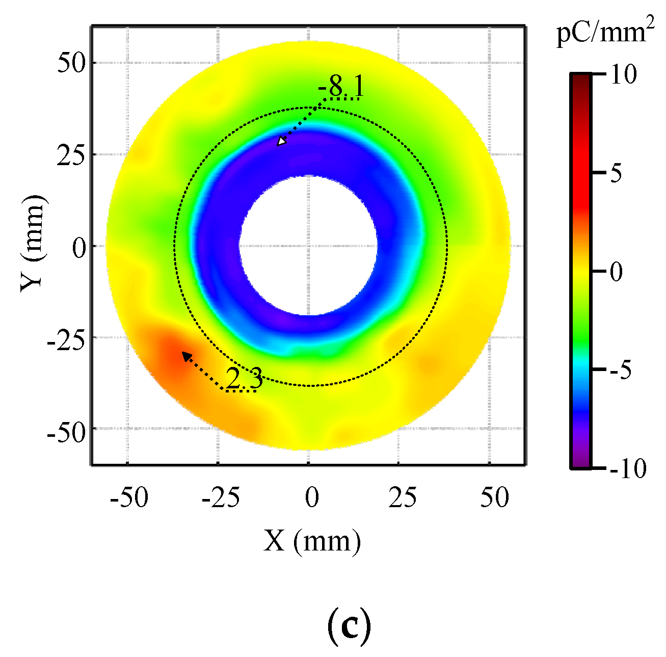
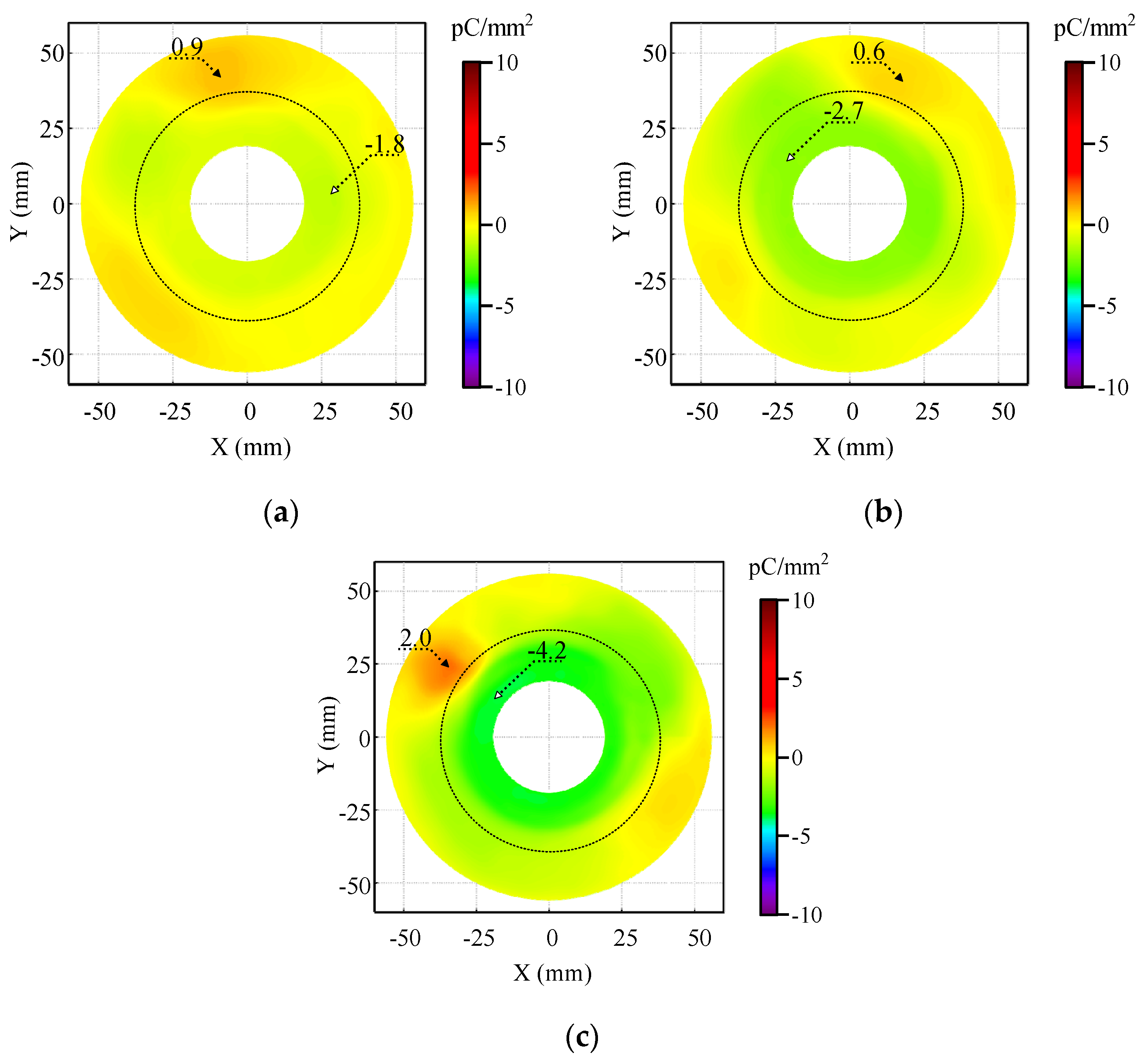
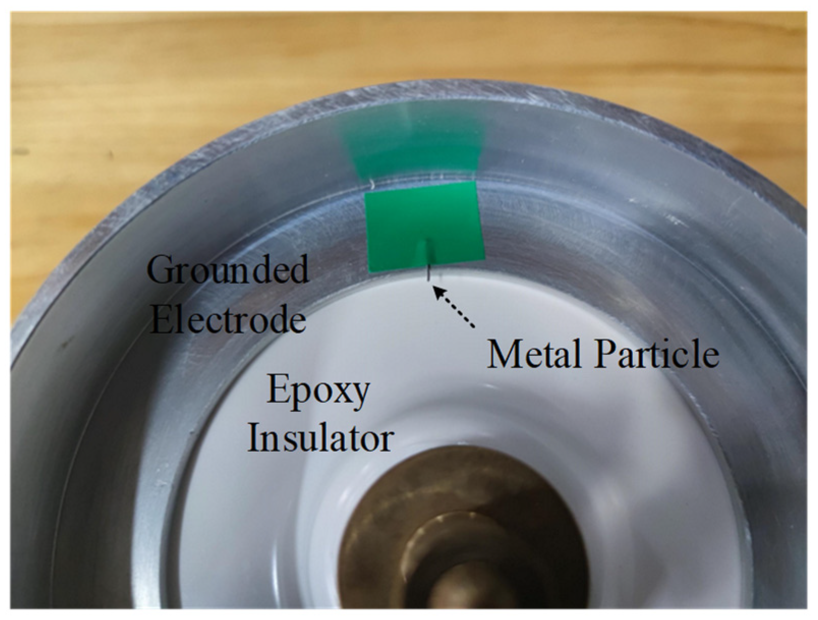
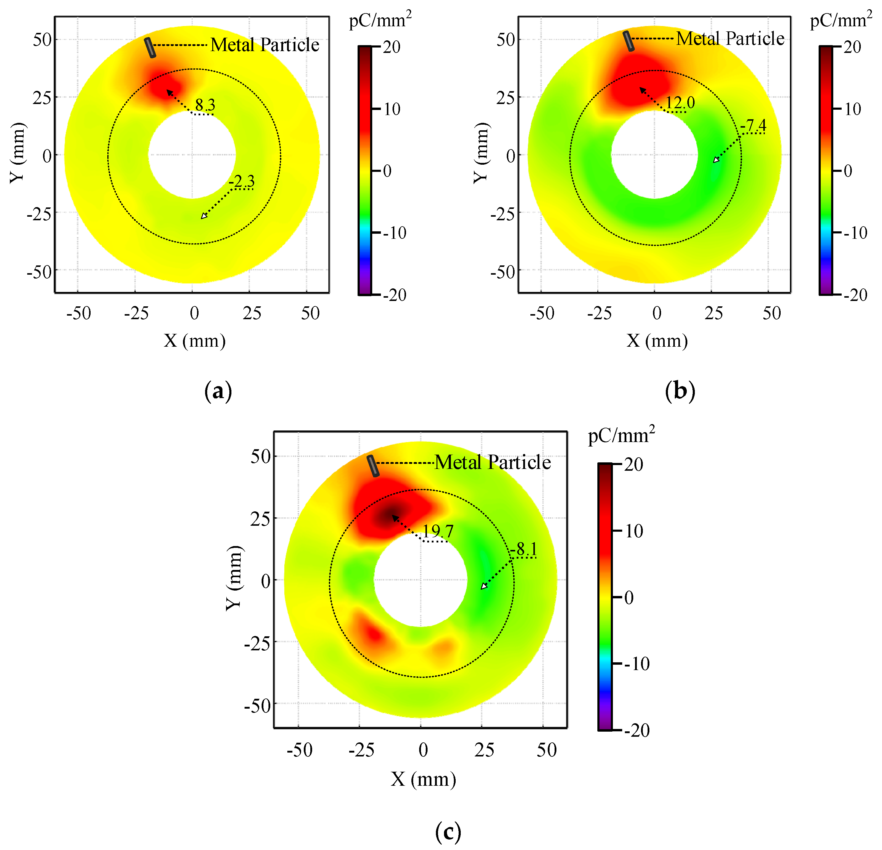
3.3. Behaviors of the Charge Accumulation on the Insulator with Metal Particle

When metal particles are in the equipment, especially near the insulator, the zoning coating can still inhibit the charge accumulation. In order to study the inhibition effect of zoning coating on the charge accumulation in the presence of a strong discharge source, a linear aluminum metal particle with a diameter of 0.5 mm and a length of 10 mm was employed. As the metal particle is contacted with the grounded electrode, the charge accumulation is more significant than those with particles adhering to other areas [16]. In order to simulate the worst case, the metal particle was adhered to and stretched out from the edge of the grounded electrode for 5 mm, as shown in Figure 8.
With the metal particle adhered to the grounded electrode, the typical distribution of the charge accumulation on the uncoated insulator is shown in Figure 9. A positive charge speckle with a maximum charge density of 8.3 pC/mm2 is formed in the nonplanar region under −15 kV. A larger charge speckle is observed under −20 kV. With the increase in voltage, the area of the positive charge speckle is further enlarged. The maximum charge density in the area covered by the positive charge speckle increases from 12.0 pC/mm2 under −20 kV to 19.7 pC/mm2 under −25 kV.
The typical charge distributions of the insulator with zoning coating with the presence of the metal particle under −15, −20, and −25 kV are shown in Figure 10. Unlike the distribution of surface charges on the insulator without the metal particle in Figure 3, a positive charge speckle appears in the nonplanar region. This is because metal particles can distort the surrounding electric field and induce gas ionization. The ionized positive charges move to the insulator surface and negative charges move to the grounded electrode under the action of the electric field. Therefore, a positive charge speckle is formed in the nonplanar region near the metal particle. The area covered by the charge speckle of the insulator with zoning coating is smaller than that of the uncoated insulator under the same voltage. Under −15, −20, and −25 kV, the maximum positive charge densities of the insulator surface with zoning coating are 2.6, 4.8, and 8.3 pC/mm2, respectively. Compared with Figure 9, the effects of the charge suppression are 68.7%, 60.0%, and 57.9%, which are even better than that without metal particles.

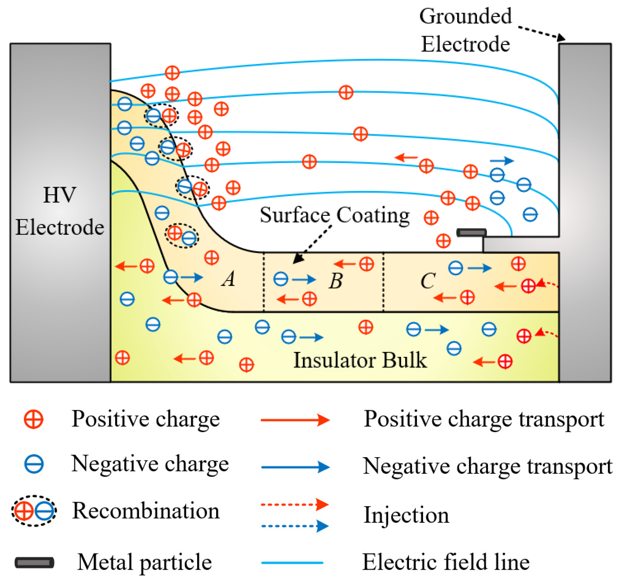
4. Inhibition Mechanism of Zoning Coating on Surface Charge Accumulation

It has been reported that the charge density on the insulator is determined by bulk, gas, and surface conduction [20]. It can be considered that the accumulation of surface charge is the result of the superposition of these three kinds of conductions. The method of calculating these three conduction current densities is given by [21],
J V = D t + γ v E b n
J G = D t + e ( μ + n + + μ n ) E g n e ( D + n + D n )
J S = ( E t γ s )
where JV, JG, and JS are the current densities through bulk, gas, and surface, respectively. e is the elementary charge. D is the electric flux density. Ebn and Egn are the normal electric fields in insulator bulk and gas. Et is the tangential electric field along the insulator surface. γv and γs are the volume and the surface conductivities. μ+, μ and D+, D are the mobility and the diffusion coefficient of positive and negative ions, respectively. n+ and n are positive and negative charge carrier densities. The charge density σ can be described as follows [22,23],
σ t = J V J G J S
When the negative voltage is applied to the HV electrode, the direction of the electric field is from gas to the insulator. In the nonplanar region, there is a strong normal component of the electric field, and the direction points to the insulator from the gas. The negative charges in the insulator tend to migrate from the bulk to the surface. In addition, the positive charges in the gas tend to move to the insulator surface. As there is no obvious discharge source in the gas without the presence of the metal particle, the ion pair generation rate in the gas is low so the gas conduction is weak. The bulk conduction is dominant in the process of charge accumulation so negative charges are accumulated in the nonplanar region. In the planar region, there is a strong tangential component of the electric field, and the direction points to the central conductor from the grounded electrode. Therefore, the positive charges injected by the grounded electrode are deposited in the planar region near the grounded electrode.
With the presence of the zoning coating, there is no change in the bulk and gas conductions but the surface conduction is changed. Surface conductivity plays a major role in the dissipation of the surface charge because the coating is quite thin. In area A, the surface conductivity increases from 1.3 × 10⁻¹⁸ S to 3.98 × 10⁻¹⁷ S after the insulator is coated by epoxy/GR coating. The coating with high insulator conductivity promotes the dissipation of the surface charge. Therefore, the charges accumulated in the nonplanar area are reduced and the charge accumulation is effectively restrained. In area C, in order to reduce the charges injected by the grounded electrode, the low-conductivity coating consisting of epoxy and Al2O3 is applied. As the surface conductivity decreases to 1.27 × 10⁻¹⁹ S, the charge transportation caused by the tangential electric field is suppressed. In area B, an epoxy/SiC coating with nonlinear conductivity is used as a transition between areas A and C. The conductivity of the epoxy/SiC mixture will increase with the increase in the electric field strength and the effect of accelerating charge dissipation is more obvious.
When the metal particle is adhered to the grounded electrode, due to the small radius of curvature of the tip of the metal particle, the gas is prone to ionize under a strong electric field, producing a large number of positive and negative ions. The gas conduction is dominant in the process of charge accumulation. Because the direction of the electric field is from the ground electrode to the central conductor under negative voltage, the positive charge is transported to the nonplanar area, and the negative charge is absorbed by the grounded electrode. Due to the strong normal component of the electric field in the nonplanar area, a large number of positive charges are accumulated in the nonplanar area of the insulator to form the positive charge speckle. The dynamic diagram of the charge on the insulator surface under the zoning coating is shown in Figure 11, in which the blue line is the electric field line, and the linear metal particles are represented by black line segments. As the insulator surface is coated with zoning coating, positive charges are more easily able to migrate in the nonplanar region and are accumulated with lower density because of the coating with high conductivity; they are then neutralized by the negative charges transported from the insulator bulk. Therefore, the area covered by the positive charge speckle and the maximum charge density of the insulator with zoning coating is smaller than that of the uncoated insulator under the same voltage.

5. Conclusions

In this paper, the downsized insulator is taken as the research object, the charge accumulation behaviors on the insulator surface under negative DC voltage are studied, and a zoning coating strategy to suppress the charge accumulation is proposed. The influence of metal particle on surface charge distribution with the zoning coating is discussed. The main conclusions are summarized as follows:
1. When the negative voltage is applied to the HV electrode, negative charges are mainly accumulated in the nonplanar region of the insulator surface. In addition, positive charges are accumulated near the grounded electrode. The charge density profile along the radial direction shows a single-peak distribution feature. The peak value of the charge density increases and the maximum value occurs in the nonplanar area at the radial length of about 25 mm from the central conductor of the insulator.
2. With the presence of the metal particle, an extra charge speckle is formed in the nonplanar region. The gas conduction dominates the charge accumulation process. The maximum charge density of positive charges increases with the increase in applied voltage.
3. The zoning coating, which is achieved by coating region A with a high-conductivity material, region C with a low-conductivity material, and region B with a nonlinear-conductivity material, can inhibit the accumulation of charge with and without the presence of the metal particle. The maximum charge densities are reduced by the coating. The inhibition effect of the charge accumulation with the presence of the metal particle is better than that without the presence of the metal particle.
In summary, it is found that zoning coating can effectively inhibit the charge accumulation on the insulator surface, especially in the presence of the metal particle. Such a finding will be helpful for the design and the safe operation of the insulator in DC GILs.

Author Contributions

Data curation, H.Z.; Formal analysis, W.W.; Investigation, H.Z.; Methodology, Y.G.; Resources, Y.G.; Writing—original draft, H.Z.; Writing—review and editing, W.W. and Y.G. All authors have read and agreed to the published version of the manuscript.

Funding

This work is financially supported by State Grid Tianjin Electric Power Company (5500-202099277A-0-0-00).

Conflicts of Interest

The authors declare no conflict of interest.

References

  1. Qi, B.; Zhang, G.; Li, C.; Gao, C.J.; Zhang, B.Y.; Chen, Z.Z. Research Status and Prospect of Gas-insulated Metal Enclosed Transmission Line. High Volt. Eng. 2015, 41, 1466–1473. [Google Scholar]
  2. Kumara, S.; Serdyuk, Y.; Gubanski, S. Simulation of Surface Charge Effect on Impulse Flashover Characteristics of Outdoor Polymeric Insulators. IEEE Trans. Dielec. Electr. Insul. 2010, 17, 1754–1763. [Google Scholar] [CrossRef]
  3. Hosokawa, M.; Endo, F.; Yamagiwa, T.; Ishokawa, T. Particle-Initiated Breakdown Characteristics and Reliability Improvement in SF6 Gas Insulation. IEEE Trans. Power Deliv. 1986, 1, 58–65. [Google Scholar] [CrossRef]
  4. Li, C.; Lin, C.; Zhang, B.; Li, Q.; Liu, W.; Hu, J.; He, J. Understanding Surface Charge Accumulation and Surface Flashover on Spacers in Compressed Gas Insulation. IEEE Trans. Dielec. Electr. Insul. 2018, 25, 1152–1166. [Google Scholar] [CrossRef]
  5. Ma, J.; Zhang, Q.; Wu, Z.; Guo, C.; Wen, T.; Wang, G.; Gao, C. Breakdown characteristics of particle-contaminated HVDC GIL under superimposed voltage of DC and impulse. IEEE Trans. Dielec. Electr. Insul. 2018, 25, 1439–1447. [Google Scholar] [CrossRef]
  6. Hara, M.; Maeda, Y.; Nakagawa, N.; Suehiro, J.; Yamada, S. DC breakdown voltage characteristics of saturated liquid helium in the presence of metallic particles. IEEE Trans. Dielectr. Electr. Insul. 2006, 13, 470–476. [Google Scholar] [CrossRef]
  7. Gao, Y.; Wang, H.; Yuan, X.; Zhao, H.; Li, Z. Surface Charge Accumulation on a Real Size Epoxy Insulator With Bouncing Metal Particle Under DC Voltage. IEEE Trans. Plasma Sci. 2021, 49, 2166–2175. [Google Scholar] [CrossRef]
  8. Wang, Z.; Wang, J.; Li, Q.; Liu, S. 3D Simulation and Experimental Study of Metal Particles’ Effect in DC GIL on Surface Charge Accumulation. Proc. CSEE 2016, 36, 6718–6726+6925. [Google Scholar]
  9. Li, B.; Wang, J.; Zhang, S. Influence of the DC-GIL Conductive Adherent Particles on the Charge Accumulation of Insulator Surface. High Volt. App. 2017, 53, 80–86. [Google Scholar]
  10. Cheng, H.; Wei, W.; Zhang, L.; Zou, L.; Zhao, T. Study on Linear Metal Particle Motion and Electrode-coating in DC GIL. In Proceedings of the 2021 International Conference on Advanced Electrical Equipment and Reliable Operation (AEERO), Beijing, China, 15–17 October 2021; pp. 1–4. [Google Scholar]
  11. Shao, T.; Liu, F.; Hai, B.; Ma, Y.; Wang, R.; Ren, C. Surface modification of epoxy using an atmospheric pressure dielectric barrier discharge to accelerate surface charge dissipation. IEEE Trans. Dielectr. Electr. Insul. 2017, 24, 1557–1565. [Google Scholar] [CrossRef]
  12. Qi, B.; Gao, C.; Lv, Y.; Li, C.; Tu, Y.; Xiong, J. The impact of nano-coating on surface charge accumulation of epoxy resin insulator: Characteristic and mechanism. J. Phys. D Appl. Phys. 2018, 51, 245303. [Google Scholar] [CrossRef]
  13. Gao, Y.; Yuan, X.; Wang, H.; Wang, M.; Li, Z.; Han, T. Graphene oxide addition with low fraction improving surface charge inhibition performance of epoxy/SiC coating under DC stress. IEEE Access 2020, 8, 11165–11173. [Google Scholar] [CrossRef]
  14. Xue, J.Y.; Chen, J.H.; Dong, J.H.; Wang, H.; Li, W.D.; Deng, J.B.; Zhang, G.J. The regulation mechanism of SiC/epoxy coatings on surface charge behavior and flashover performance of epoxy/alumina spacers. J. Phys. D Appl. Phys. 2019, 52, 405502. [Google Scholar] [CrossRef]
  15. Li, J.; Liang, H.C.; Du, B.X.; Wang, Z.H. Surface functional graded spacer for compact HVDC gaseous insulated system. IEEE Trans. Dielectr. Electr. Insul. 2019, 26, 664–667. [Google Scholar] [CrossRef]
  16. Gao, Y.; Li, Z.; Wang, H.; Yuan, X. Metal particle encouraged surface charge accumulation on epoxy insulator with multi-arc surface profile under DC voltage. IEEE Trans. Dielec. Electr. Insul. 2020, 27, 998–1006. [Google Scholar] [CrossRef]
  17. Gao, Y.; Wang, H.; Li, Z.; Yuan, X.; Zhao, H. Gaseous ionization dependence of surface charge pattern on epoxy insulator with complex surface profile under DC voltage. IEEE Trans. Dielec. Electr. Insul. 2021, 49, 1627–1635. [Google Scholar] [CrossRef]
  18. Zhang, B.; Zhang, G.; Wang, Q.; Li, C.; He, J.; An, Z. Suppression of surface charge accumulation on Al2O3-filled epoxy resin insulator under DC voltage by direct fluorination. AIP Adv. 2015, 5, 127207. [Google Scholar] [CrossRef] [Green Version]
  19. Kumada, A.; Okabe, S.; Hidaka, K. Residual charge distribution of positive surface streamer. J. Phys. D Appl. Phys. 2009, 42, 095209. [Google Scholar] [CrossRef]
  20. Li, C.; Fu, J.; Zi, Y.; Cao, Y. Insulator Surface Charge Behaviors: From Hazards to Functionality. IEEE Electr. Insul. Mag. 2022, 38, 6–14. [Google Scholar] [CrossRef]
  21. Winter, A.; Kindersberger, J. Transient Field Distribution in Gas-Solid Insulation Systems under DC Voltages. IEEE Trans. Dielec. Electr. Insul. 2014, 21, 116–128. [Google Scholar] [CrossRef]
  22. Kindersberger, J.; Lederle, C. Surface charge decay on insulators in air and sulfurhexafluorid—Part I: Simulation. IEEE Trans. Dielec. Electr. Insul. 2008, 15, 941–948. [Google Scholar] [CrossRef]
  23. Winter, A.; Kindersberger, J. Stationary Resistive Field Distribution along Epoxy Resin Insulators in Air under DC Voltage. IEEE Trans. Dielec. Electr. Insul. 2012, 19, 1732–1739. [Google Scholar] [CrossRef]
Figure 1. Test insulator.
Energies 15 04730 g001
Figure 2. Insulator profile and electrode size.
Energies 15 04730 g002
Figure 3. Typical charge distribution on insulator without coating under different voltages. (a) Typical charge distribution under −15 kV; (b) Typical charge distribution under −20 kV; (c) Typical charge distribution under −25 kV.
Energies 15 04730 g003aEnergies 15 04730 g003b
Figure 4. Diagram of zoning coating on the insulator surface.
Energies 15 04730 g004
Figure 5. Relationship between bulk conductivity and applied electric field of epoxy/SiC coating.
Energies 15 04730 g005
Figure 6. Typical charge distribution on insulator with zoning coating under different voltages. (a) Typical charge distribution under −15 kV; (b) Typical charge distribution under −20 kV; (c) Typical charge distribution under −25 kV.
Energies 15 04730 g006
Figure 7. Radial distribution of average charge density on insulator surface with and without zoning coating.
Energies 15 04730 g007
Figure 8. Schematic diagram of metal particle placement.
Energies 15 04730 g008
Figure 9. Typical charge distribution on the insulator without zoning coating with the metal particle under different voltages. (a) Typical charge distribution under −15 kV; (b) Typical charge distribution under −20 kV; (c) Typical charge distribution under −25 kV.
Energies 15 04730 g009
Figure 10. Typical charge distribution on the insulator with zoning coating with the metal particle under different voltages. (a) Typical charge distribution under −15 kV; (b) Typical charge distribution under −20 kV; (c) Typical charge distribution under −25 kV.
Energies 15 04730 g010
Figure 11. Schematic diagram of surface charge accumulation with metal particle adhered to the grounded electrode under negative voltage.
Energies 15 04730 g011
Table 1. Conductivity of different samples.
SampleBulk Conductivity (S/m)Surface Conductivity (S)
Reference2.3 × 10−151.3 × 10⁻¹⁸
Al2O3-1 wt%4.04 × 10−159.35 × 10⁻¹⁹
Al2O3-3 wt%4.94 × 10−151.27 × 10⁻¹⁹
GR-1 wt%5.18 × 10−153.95 × 10⁻¹⁸
Publisher’s Note: MDPI stays neutral with regard to jurisdictional claims in published maps and institutional affiliations.

