Abstract
This paper analyzes two different design procedures for a series-parallel compensated WPT battery charger, based on different definitions of the operating resonant frequency in the condition of maximum link efficiency. The behaviour of the voltage gain magnitude and the input impedance angle of the resulting WPT links is studied for different loads and coupling coefficients. The design algorithms are supported by analytical formulas derived from an exact circuit analysis of the WPT link, avoiding approximations as far as possible. To support the theoretical approach a case study is proposed, in which both design procedures are implemented considering specifications in line with the actual automotive standards. To conclude, a characterization of the efficiency in both cases is derived.
1. Introduction
Nowadays, environmental issues and technological improvements have pushed towards the direction of investing in electric mobility. The last frontier of power electronics and modern Li-ion batteries have made battery electric vehicles (BEV) and plug-in electric vehicles (PHEV) an efficient, low polluting and reliable alternative to traditional vehicles fed by fossil fuels. However, both BEV and PHEV suffer from problems related to the charging time and therefore charging at high power rating becomes fundamental. The charging problem is further aggravated when operating in harsh environments. Moreover, dangerous limitations of on-board chargers (OBCs) refer to safety of operation, reliability and need to manually connect the car to a charging station. To overcome these limitations, Wireless Power Transfer (WPT) systems have become an hot-spot to be further analyzed [1,2,3]. A typical DC/DC stage for a WPT system is split into two parts according to their positions either on- or off-board the vehicle. The off-board layout mounted on the ground assembly (GA) starts from the rectified DC bus voltage, , which is provided by the AC/DC stage. Then, it goes through the full-bridge inverter, that feeds the primary resonant tank, up to the primary transmitter coil. The receiver coil, positioned at the bottom of the car, is the first on-board component of the vehicle assembly (VA). It is directly connected to a secondary resonant tank and to a full-bridge diode rectifier [1,2]. Inside the car, an additional DC/DC converter takes care of charging the battery pack by means of a proper algorithm control able to track the constant-current-constant-voltage (CC-CV) charging cycle. The whole DC/DC stage is shown in Figure 1.
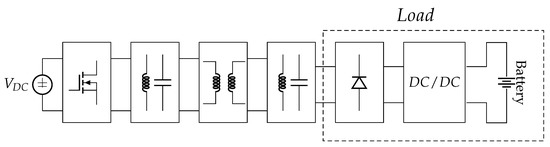
Figure 1.
DC/DC power conversion stage for a WPT battery charger system, starting from the rectified voltage up to the load.
In addition, improper charging cycles that exceed upper and lower bounds along with battery usage result in a increase of the battery internal resistance (resistance growth) and in a decrease of the battery rated capacity (capacity fade). Therefore, it becomes necessary to estimate the battery State of Health (SOH) [4] from cell-level tests. The battery capacity can also be monitored through Data-Driven methods with the aim to assess the remaining useful life (RUL) [5]. Depending on the desired characteristics, several combinations of primary and secondary resonant circuits are available and analyzed in literature [6]. Basic resonant topologies, such as series-series (SS) and series-parallel (SP), have been deeply studied and compared [7]. Parallel-series (PS) and parallel-parallel (PP) are not of interest for battery charging applications, since the voltage applied to the tank is imposed by the inverter and an additional inductor must be connected in series between the inverter output port and the resonant tank [8], whose value may not be negligible.
A procedure design for the SS topology is given in [9,10] and what turns out is its relatively simple design, but with some difficulties in following the CC-CV charging cycle together with achieving zero-phase angle (ZPA). SS and SP are only able to operate either in CC mode with ZPA or CV mode with ZPA, but not in both [8]. Although [11] proposed a control system able to follow the CC-CV charging cycle for SP, it does not guarantee ZPA, which can be achieved by means of hybrid compensations [12]. By increasing the number of components, with a double side inductor-capacitor-capacitor (LCC-LCC) it is possible to fulfill both the CC-CV reference profiles and the ZPA condition. On the other hand, it requires many components, leading to an increase in size, power losses and control system complexity. The latter method becomes meaningless when the self-inductance of the primary side differs from the secondary one [8]. Also, the multiple-input-multiple-output (MIMO) configuration can be adopted in automotive applications. Reference [13] proposes a general design procedure, valid for any strictly–passive multi–port network, based on optimal impedance terminations for efficiency maximization. The efficiency can also be maximized for resonance frequency mismatch [14] or estimated using numerical and circuit models [15]. Multicoil systems have been also proposed in [16,17] to extend the transmission region and thus overcome the problem of the misalignment between the GA and VA coils, which can lead to severe components stress and disturbances [18,19,20], besides hazard magnetic fields [21,22]. However, when referring to automotive apparatuses, the size and weight of the components are fundamental parameters that have to be minimized. Regardless of the primary side topology, the parallel secondary compensation exhibits a much lower secondary self-inductance, when compared to the series one [23] and therefore it is preferred for automotive applications. Besides, all the above-mentioned papers consider the primary and secondary self-inductances of the resonant tank as input values, therefore they are not optimized for the target application.
This paper aims at providing a general design procedure, including the coil design, based on maximizing the tank efficiency and minimizing the VA self-inductance, considering the SP compensation network topology for automotive battery charging applications.
2. Design Procedure
The design and tailoring of inductive couplers should be coordinated with both the compensation topology and the type of load, since both of them contribute to the overall system efficiency. The main goal is the transmission of the desired power through a certain control strategy based on load requirements, minimization of losses and optimization of system efficiency, coil size and weight. Figure 2 illustrates the adopted design procedure step by step taking into account the following points:
Figure 2.
Flow chart illustrating the design algorithm for the inductive coupling and the compensation networks based on the selected output characteristic. The load resistance and the coupling coefficient k refer to actual parameters during variable operating conditions.
- SP compensation network
- Maximize the system efficiency
- Lightweight vehicle assembly
- Fulfil the required voltage gain
- Zero voltage switching (ZVS)
- Minimize the circulation of reactive power
The first design step consists in modelling the load by means of a proper equivalent resistance , as discussed in Section 2.1. Then, a reference value for the load equivalent resistance must be chosen. The same holds for the coupling coefficient k between the GA and VA coils, which is generally defined as:
where and are the self-inductance coefficients of the GA and VA windings, respectively, while M is their mutual inductance coefficient. A reference coupling coefficient value must be considered for the design. Once and are defined, the design passes through the choice of the secondary capacitor . Straightforwardly, the secondary inductor can be sized to make the receiver resonate at the desired frequency . Two different design procedures are proposed for achieving either a CV or ZPA at the desired resonant frequency. Pole splitting and bifurcation phenomena can be avoided deviating the proposed design rule for the inductance of about 15–20% [24]. Once the receiver parameters have been found, the primary inductance can be designed according to the desired voltage gain of the converter, which is defined as:
with and the phasors associated to the input and output voltages of the inductive link and , resepctively, as depicted in Figure 3. This parameter clearly depends on the particular primary compensation network and its tuning. The lumped capacitor connected in series to is usually designed to make the input impedance of the inductive coupling purely real at the design resonant frequency .
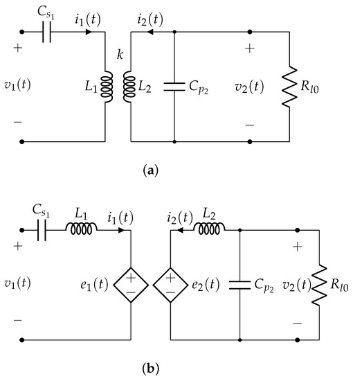
Figure 3.
Equivalent circuits of the resonant inductive link where the inductive coupling is represented by means of (a) two coupled inductors and (b) two decoupled inductors with series controlled voltage sources.
2.1. Load Modelling
For battery charging applications, the load of the inductive link comprises a full-bridge diode rectifier followed by a second order filter, which feeds the DC link of the DC/DC converter that regulates the battery current and voltage. According to [25], in the hypothesis of ideal components, the overall load circuit seen at the terminals of the secondary side can be considered as an equivalent resistance defined as:
where is the chopper DC link voltage and the power delivered to the battery.
2.2. Load Matching
According to [26], a total link efficiency can be defined as:
where is the phasor voltage across the primary coil and its phasor current. After some mathematical manipulations, it can be rewritten as:
where and are the quality factors of the primary and secondary coils, respectively, the coupling coefficient between the primary and secondary coil and with the angular frequency associated to the operating frequency . This expression does not consider the primary compensation and thus it is valid for any topology. Moreover, no hypothesis has been done on the tuning of the receiver resonant frequency, which can be arbitrarily chosen, as it is discussed later on. Assuming high values of the quality factors and , for given k and it is possible to find the optimum value of secondary-capacitive admittance that maximises the efficiency. It is obtained enforcing
that leads to the following optimum value of , considering the reference coupling coefficient :
Then, at the design resonant frequency , the optimum capacitance value for a reference load results:
2.3. Design for Constant Voltage Output
A SP compensated resonant inductive link can achieve constant output voltage at the chosen and coupling coefficient when designed such that:
where:
with and the self-inductances of the GA and VA coils, respectively, and and the lumped capacitances of the GA and VA compensation networks, respectively. Then, the optimal value of can be obtained from (9) considering (8) as:
or, equivalently,
For this configuration, the voltage gain can be written as:
The optimal value of the primary inductance can be matched considering the condition of maximum efficiency of the inductive link, for which the voltage gain can be rearranged introducing . After some mathematical manipulations, it holds:
The only missing component is the primary capacitor, which can be easily designed as:
2.4. Design for Coupling Independent ZPA
While the design of compensation networks described in (9) allows CV operations, it does not allow the imaginary part of the receiver impedance to be completely cancelled. The basic idea behind resonant circuits is to reduce the amount of reactive power required by the circuit for a fixed active power. It corresponds to eliminate the imaginary component of the circuit impedance, which is, in this case, the impedance seen by the (ideal) controlled voltage source representing the secondary induced voltage, as it can be seen in Figure 3b. For a receiver with parallel compensation, the impedance can be expressed as:
and thus it is possible to have Im at if:
However, it should be noticed that presents a “residual” real term, which is due to the particular compensation topology and cannot be cancelled. The ideal receiver impedance can be considered the pure load , but this condition can be achieved only with an imaginary resonant frequency, which is, of course, meaningless. From (18), it is possible to find the optimal secondary inductance value at as:
or, equivalently,
In case the receiver is tuned according to (18), a real input impedance simply requires and to be sized such that:
In this condition, the voltage gain amplitude results:
Introducing it leads to an optimal primary inductance value defined as:
and thus the primary capacitor can be sized as:
3. Case Study
The design procedures presented in the previous section are applied to a real test case, made of a battery pack and a charging system for automotive applications. The specifications required for the inductive link design are given in the first part of Table 1, while the second and third part list the inductive link components. To start the procedure, the required design guesses are:

Table 1.
Case study system parameters.
- Inductor quality factors and ;
- Reference coupling coefficient .
For both the proposed design procedures, the secondary inductance results about four times lower with respect to the primary one , confirming the theoretical predictions. Moreover, the comparison between (12) and (20) suggests that the tuning method proposed in (18) leads to a smaller secondary inductance, for given values of , and . In addition, studying the trends of and as a function of it can be found that the two inductances present approximately the same value for , regardless of the particular system specifications.
The main difference between the two design procedures can be understood by means of the analytical formulas reported in Section 2 and it can be graphically visualized in Figure 4, Figure 5 and Figure 6. In particular, Figure 4a and Figure 5a show the magnitude of the voltage gain as a function of the frequency for different loads. Figure 4a clearly indicates that the voltage gain is nearly constant at the chosen , with the compensation network parameters tuned according to (9). Reversely, in case of , Figure 5a highlights that the voltage gain magnitude at varies depending on the load, especially for low values of .
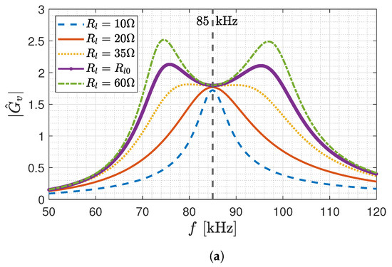
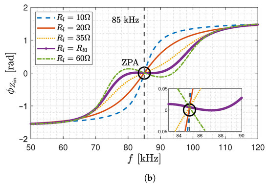
Figure 4.
(a) Voltage gain magnitude and (b) input impedance angle as a function of the frequency for the inductive link designed for working with CV operations at kHz.
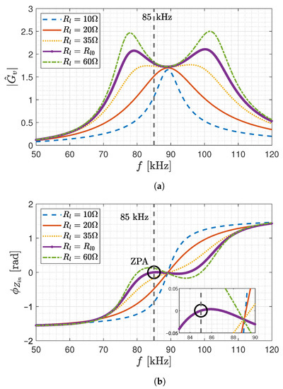
Figure 5.
(a) Voltage gain magnitude and (b) input impedance angle as a function of the frequency for the inductive link designed for coupling independent ZPA operations at kHz.
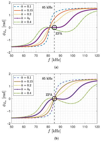
Figure 6.
Input impedance angle as a function of the frequency for different coupling coefficients in case of inductive link designed for (a) CV output and (b) coupling independent ZPA operations at kHz.
The input impedance angle defines the effective reactive demand of the WPT link and the possibility of ZVS operations. It is plotted in Figure 4b and Figure 5b as a function of the frequency and for different loads for a system designed such that and , respectively. At , the former tuning allows ZPA operations for any load, while in the latter case they are possible only if . This can be explained considering the definition of the system angular frequency, which is independent on the load for and , whereas the value of is affected by .
Another crucial parameter that affects the behaviour of the WPT link is the coupling coefficient k, which basically depends on the alignment between the GA and VA coils. The trends of the input impedance angles as a function of the frequency for different values of the coupling coefficient for and are plotted in Figure 6a,b, respectively. ZPA operations at are possible for any coupling coefficient only in the latter case, since k does not appear in the definition of and . In the case of , the input impedance angle depends on the alignment condition between the VA and GA coils, being positive for and negative for .
Efficiency Characterization
In order to validate the proposed design procedures, the efficiency of the SP compensated WPT link, whose parameters are listed in Table 1, has been calculated for different operating conditions. Figure 7 represents, in logarithmic scale, the efficiency calculated unless iron and diodes losses as a function of the equivalent load resistance for different coupling coefficients k, for a system designed for CV or coupling independent ZPA. The operating frequency is kHz. Overall, Figure 7 shows that for a certain value of the efficiency is higher as the coupling coefficient increases, while the maximum of the efficiency curve occurs in correspondence of higher equivalent loads as the coupling coefficient decreases. In general, the tuning for coupling independent ZPA, namely for , guarantees a slightly higher efficiency with respect to the tuning for CV operations, obtained with . This is due to the tuning of the secondary capacitor, which perfectly cancels the imaginary part of the receiver impedance only if . However, as expected, for , the systems designed for CV and coupling independent ZPA operations present the same efficiency, and this occurs for any k. In particular, for , the efficiency at is maximum, with a value of 97.8%. The main difference between the efficiency trends, resulting from the two different design procedures, is more evident for high equivalent loads, where the curves obtained with the CV design overlap, unlike the ones resulting from the coupling independent ZPA design.
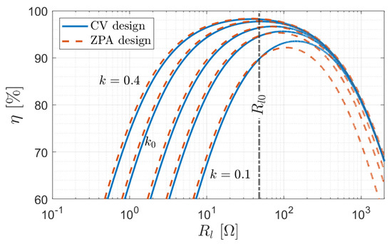
Figure 7.
Overall link efficiency of a WPT system designed for CV or coupling independent ZPA, operating at , as a function of the receiver equivalent load , for different coupling coefficients k.
4. Conclusions
Despite the resulting values of the inductive link parameters are quite similar, this analysis has highlighted that the behaviour of the system for different load and coupling coefficient values is different. For a given operating frequency, it is possible to achieve CV operations in ZPA conditions for any receiver load. However, at that frequency, the input impedance strongly varies depending on the coupling coefficient, preventing ZPA operations with a consequent drop of the system efficiency. Reversely, an alternative tuning able to ensure constant ZPA operations at the chosen resonant frequency is possible, with the drawbacks of load-dependent voltage gain and input impedance angle. Moreover, this tuning allows the perfect compensation of the receiver impedance reducing the reactive power demand. At a certain induced voltage, it experiences lower current, with a consequent increase in the efficiency. This is confirmed by the efficiency analysis, which also verified that, for , efficiency values of about are guaranteed for a wide range of loads . As expected, the secondary inductance results much smaller than the primary one, meaning that the VA coil is much lighter than the GA one. Overall, both the proposed compensations present pros and cons and thus they have to be chosen depending on the target application.
Author Contributions
Conceptualization, M.S. and A.C.; methodology, M.S. and A.C.; software, A.C. and M.S.; investigation, M.S. and A.C.; resources, M.S.; writing—original draft preparation, M.S. and A.C.; writing—review and editing, M.S., A.C., L.S. and C.R.; supervision, L.S. and C.R. All authors have read and agreed to the published version of the manuscript.
Funding
This research received no external funding.
Institutional Review Board Statement
Not applicable.
Informed Consent Statement
Not applicable.
Data Availability Statement
Data is available in the paper.
Conflicts of Interest
The authors declare no conflict of interest.
References
- Covic, G.A.; Boys, J.T. Modern Trends in Inductive Power Transfer for Transportation Applications. IEEE J. Emerg. Sel. Top. Power Electron. 2013, 1, 28–41. [Google Scholar] [CrossRef]
- Li, S.; Mi, C.C. Wireless Power Transfer for Electric Vehicle Applications. IEEE J. Emerg. Sel. Top. Power Electron. 2015, 3, 4–17. [Google Scholar]
- Patil, D.; McDonough, M.K.; Miller, J.M.; Fahimi, B.; Balsara, P.T. Wireless Power Transfer for Vehicular Applications: Overview and Challenges. IEEE Trans. Transp. Electrif. 2017, 4, 3–37. [Google Scholar] [CrossRef]
- She, C.; Zhang, L.; Wang, Z.; Sun, F.; Liu, P.; Song, C. Battery State of Health Estimation Based on Incremental Capacity Analysis Method: Synthesizing from Cell-Level Test to Real-World Application. IEEE J. Emerg. Sel. Top. Power Electron. 2021. [Google Scholar] [CrossRef]
- Wang, Z.; Song, C.; Zhang, L.; Zhao, Y.; Liu, P.; Dorrell, D.G. A Data-Driven Method for Battery Charging Capacity Abnormality Diagnosis in Electric Vehicle Applications. IEEE Trans. Transp. Electrif. 2021. [Google Scholar] [CrossRef]
- Zhang, W.; Mi, C.C. Compensation topologies of high-power wireless power transfer systems. IEEE Trans. Veh. Technol. 2016, 65, 4768–4778. [Google Scholar] [CrossRef]
- Aditya, K.; Williamson, S.S. Comparative study of Series-Series and Series-Parallel compensation topologies for electric vehicle charging. In Proceedings of the IEEE 23rd International Symposium on Industrial Electronics (ISIE), Istanbul, Turkey, 1–4 June 2014; pp. 426–430. [Google Scholar]
- Vu, V.B.; Tran, D.H.; Choi, W. Implementation of the Constant Current and Constant Voltage Charge of Inductive Power Transfer Systems with the Double-Sided LCC Compensation Topology for Electric Vehicle Battery Charge Applications. IEEE Trans. Power Electron. 2018, 33, 7398–7410. [Google Scholar] [CrossRef]
- Huang, Z.; Wong, S.C.; Tse, C.K. Design methodology of a series-series inductive power transfer system for electric vehicle battery charger application. In Proceedings of the IEEE Energy Conversion Congress and Exposition (ECCE), Pittsburgh, PA, USA, 14–18 September 2014; pp. 1778–1782. [Google Scholar]
- Zhang, W.; Wong, S.C.; Tse, C.K.; Chen, Q. Design for Efficiency Optimization and Voltage Controllability of Series–Series Compensated Inductive Power Transfer Systems. IEEE Trans. Power Electron. 2014, 29, 191–200. [Google Scholar] [CrossRef]
- Simonazzi, M.; Campanini, A.; Sandrolini, L.; Rossi, C. Single Stage Wireless Power Transfer Battery Charger for Electric Vehicles. In Proceedings of the IEEE 15th International Conference on Compatibility, Power Electronics and Power Engineering (CPE-POWERENG), Florence, Italy, 14–16 July 2021; pp. 1–6. [Google Scholar]
- Mai, R.; Chen, Y.; Li, Y.; Zhang, Y.; Cao, G.; He, Z. Inductive Power Transfer for Massive Electric Bicycles Charging Based on Hybrid Topology Switching With a Single Inverter. IEEE Trans. Power Electron. 2017, 32, 5897–5906. [Google Scholar] [CrossRef]
- Monti, G.; Mongiardo, M.; Minnaert, B.; Costanzo, A.; Tarricone, L. Multiple Input Multiple Output Resonant Inductive WPT Link: Optimal Terminations for Efficiency Maximization. Energies 2021, 14, 2194. [Google Scholar] [CrossRef]
- Stankiewicz, J.M.; Choroszucho, A.; Steckiewicz, A. Estimation of the Maximum Efficiency and the Load Power in the Periodic WPT Systems Using Numerical and Circuit Models. Energies 2021, 14, 1151. [Google Scholar] [CrossRef]
- Weerasekara, H.; Hata, K.; Imura, T.; Fujimoto, H.; Hori, Y. Efficiency Maximization in Wireless Power Transfer Systems for Resonance Frequency Mismatch. In Proceedings of the IEEE PELS Workshop on Emerging Technologies: Wireless Power Transfer (WoW), London, UK, 18–21 June 2019; pp. 363–366. [Google Scholar]
- Pakhaliuk, B.; Shevchenko, V.; Mućko, J.; Husev, O.; Lukianov, M.; Kołodziejek, P.; Strzelecka, N.; Strzelecki, R. Optimal Rotating Receiver Angles Estimation for Multicoil Dynamic Wireless Power Transfer. Energies 2021, 14, 6144. [Google Scholar] [CrossRef]
- Simonazzi, M.; Sandrolini, L.; Zarri, L.; Reggiani, U.; Alberto, J. Model of Misalignment Tolerant Inductive Power Transfer System for EV Charging. In Proceedings of the IEEE 29th International Symposium on Industrial Electronics (ISIE), Delft, The Netherlands, 17–19 June 2020; pp. 1617–1622. [Google Scholar]
- Campi, T.; Cruciani, S.; Maradei, F.; Feliziani, M. Conducted emission of wireless power transfer charging system in electric vehicle. In Proceedings of the IEEE International Symposium on Electromagnetic Compatibility, Washington, DC, USA, 7–11 August 2017; pp. 619–622. [Google Scholar]
- Spadacini, G.; Grassi, F.; Pignari, S.A. Modelling and simulation of conducted emissions in the powertrain of electric vehicles. Prog. Electromagn. Res. B 2016, 69, 1–15. [Google Scholar] [CrossRef][Green Version]
- Simonazzi, M.; Sandrolini, L. Conducted Emission Analysis of a Near-Field Wireless Power Transfer System. In Proceedings of the IEEE 15th International Conference on Compatibility, Power Electronics and Power Engineering (CPE-POWERENG), Florence, Italy, 14–16 July 2021; pp. 1–6. [Google Scholar]
- 16ENG08 EMPIR MICEV Consortium. Best Practice Guide for the Assessment of EMF Exposure from Vehicle Wireless Power Transfer Systems; Guilizzoni, R., Harmon, S., Zucca, M., Eds.; 17 February 2021. Available online: https://hal.archives-ouvertes.fr/hal-03312964/document (accessed on 5 November 2021).
- Cruciani, S.; Campi, T.; Maradei, F.; Feliziani, M. Active Shielding Design and Optimization of a Wireless Power Transfer (WPT) System for Automotive. Energies 2020, 13, 5575. [Google Scholar] [CrossRef]
- Bosshard, R.; Kolar, J.W.; Mühlethaler, J.; Stevanović, I.; Wunsch, B.; Canales, F. Modeling and η - α-pareto optimization of inductive power transfer coils for electric vehicles. IEEE J. Emerg. Sel. Top. Power Electron. 2015, 3, 50–64. [Google Scholar] [CrossRef]
- Wang, C.S.; Covic, G.; Stielau, O. Power transfer capability and bifurcation phenomena of loosely coupled inductive power transfer systems. IEEE Trans. Ind. Electron. 2004, 51, 148–157. [Google Scholar] [CrossRef]
- Steigerwald, R.L. A Comparison Of Half-Bridge Resonant Converter Topologies. IEEE Trans. Power Electron. 1988, 3, 174–182. [Google Scholar] [CrossRef]
- Schuylenbergh, K.V.; Puers, R. Inductive Powering: Basic Theory and Application to Biomedical Systems, 1st ed.; Springer Science: Berlin, Germany, 2009. [Google Scholar]
Publisher’s Note: MDPI stays neutral with regard to jurisdictional claims in published maps and institutional affiliations. |
© 2021 by the authors. Licensee MDPI, Basel, Switzerland. This article is an open access article distributed under the terms and conditions of the Creative Commons Attribution (CC BY) license (https://creativecommons.org/licenses/by/4.0/).