Article

Self-Balancing Supercapacitor Energy Storage System Based on a Modular Multilevel Converter

by
Fernando Davalos Hernandez
1,2,*,
Rahim Samanbakhsh
1,
Federico Martin Ibanez
1 and
Fernando Martin
3,4
1
Department of Electrical Engineering, Skolkovo Institute of Science and Technology, 143026 Moscow, Russia
2
Facultad de Ingeniería, Universidad Panamericana, Aguascalientes 20296, Mexico
3
CEIT-Basque Research and Technology Alliance (BRTA), Manuel Lardizabal 15, 20018 Donostia, Spain
4
Teoría do sinal e comunicacións, Universidad de Navarra, Tecnun, Manuel Lardizabal 13, 20018 Donostia, Spain
*
Author to whom correspondence should be addressed.
Energies 2022, 15(1), 338; https://doi.org/10.3390/en15010338
Submission received: 11 November 2021 / Revised: 6 December 2021 / Accepted: 20 December 2021 / Published: 4 January 2022

Abstract

:
Energy Storage Systems (ESS) are an attractive solution in environments with a high amount of renewable energy sources, as they can improve the power quality in such places and if required, can extend the integration of more renewable sources of energy. If a large amount of power is needed, then supercapacitors are viable energy storage devices due to their specific power, allowing response times that are in the range of milliseconds to seconds. This paper details the design of an ESS that is based on a modular multilevel converter (MMC) with bidirectional power flow, which reduces the number of cascaded stages and allows the supercapacitors SCs to be connected to the grid to perform high-power transfers. A traditional ESS has four main stages or subsystems: the energy storage device, the balancing system, and the DC/DC and DC/AC converters. The proposed ESS can perform all of those functions in a single circuit by adopting an MMC topology, as each submodule (SM) can self-balance during energy injection or grid absorption. This article analyses the structure in both power flow directions and in the control loops and presents a prototype that is used to validate the design.

1. Introduction

Supercapacitors (SCs) have the highest power density relative to Li-ion batteries, flywheels, fuel cells, and superconducting magnetic energy storage systems [1,2]. Although SC technology is still maturing, this high-power density comes with a cost, namely that SCs are usually low voltage devices, usually around 2.5 V to 3.0 V [3]. This problem can be overcome by using series connections with passive or active balancing systems, the latter being more efficient [4,5]. However, in terms of design, this added circuitry creates a more complex and expensive Energy Storage System (ESS) that is also susceptible to failure because of the many parts that are involved in the system [6,7]. Typical applications of SC-based ESSs are related to fast energy injection or absorption [8,9]. For example, in isolated microgrids with a high penetration of renewables [10], SCs maintain the power balance between consumption and generation because inertia mechanisms are limited. SCs can also be used in conjunction with batteries to create a hybrid ESS, increasing the capabilities of the system [11].
A basic SC-based ESS is composed of a balancing system, SC cells, a DC/DC converter, a DC link capacitor, and a DC/AC converter, as Figure 1 shows [8,12]. An ESS needs to keep energy storage devices balanced, protect them from overvoltage, and create the output voltage using bidirectional DC/DC and DC/AC conversions. The SC voltage changes linearly along with the state of charge, so a DC/DC converter with a wide input voltage range and a constant DC output voltage tends to be needed [13]. A DC link connects the DC/DC converter to a traditional DC/AC converter, which creates an AC signal. In addition, as galvanic isolation is important when the ESS is connected to the grid, a bulky 50Hz transformer must be used if none of the other stages has isolation, which increases the converter’s size. Each of these circuits or stages requires a careful design process in order to accomplish the power budget.
Some authors have been studying different DC/DC converter topologies for ESS that can be used for DC microgrids or for AC grids. In [14,15], the proposed converter lacks isolation, limiting its applications. In [16], an optimized supercapacitor control strategy in combination with a Double Active Bridge (DAB) is proposed, but an active or passive balancing system as well as a DC/AC inverter are still required to interact with the grid. In [17,18], the proposed converters can directly interface the energy storage device with the AC grid; however, it still requires an additional balancing system.
Instead of the traditional approach, a Modular Multilevel Converter (MMC) can be used, which is based on a high-voltage DC source and a series of submodules (SMs). In this system, DC/DC and DC/AC conversions are performed in the SMs, which consist of DC/DC converters. These MMC topologies have been used for high-voltage DC transmission [19,20]. One of the main advantages of MMCs is the simplicity of scaling up the voltage of the system by adding more SMs to the MMC [21], as shown in Figure 2a.
The relevant aspect of this work is the integration of a single SC in each of the SMs, and therefore, no high voltage DC source is needed. In addition, each SM works in a voltage range of 1.5–2.7 V, which allows the use of low-voltage switches with low conduction losses [22] and a low total harmonic distortion (THD) of the AC output voltage and current possible.
Other authors have studied low-voltage MMC [23], for example, for railway traction systems, in which each supercapacitor is integrated in every SM, but these applications have only been studied analytically [22]. Low-voltage MMC was also studied for its potential use in STATCOMs applications by incorporating the ESS into the MMC; however, this was only possible by adding an additional DC/DC converter [24]. The same occurs in power traction converters, where for adding SCs, a DC/DC converter was added [25]. In [26], the proposed MMC integrates the SCs in each SM, and a balancing strategy is presented; however, the ESS requires a bulky transformer if isolation is required.
This paper proposes an SC-based ESS using an MMC in which each SM contains an energy storage device (a single SC) and a bidirectional isolated DC/DC converter. The proposed MMC diagram is shown in Figure 2b. The DC/DC converter acts a controllable DC voltage source. Thus, the MMC becomes a series chain of controllable voltage sources and, with the correct control strategy, the SMs can create an AC output signal: vMMC(t). Therefore, the main contribution of this research is the development of an ESS that is based on an MMC that can perform the functions of energy storage, voltage balancing, and bidirectional DC/DC and DC/AC conversion with galvanic isolation in a single block (or SM), resulting in a self-balancing MMC that is easily expandable to higher voltages and that is controllable with a central controller. A prototype validates the proposed ESS, and the prototype shows how the circuit works; however, the efficiency is not optimized and can be further improved through the use of GaN or SiC transistors.
This paper is structured as follows. Section 2 presents SM operation in both power flow directions. Section 3 details the MMC operational modes and the self-balancing control that is embedded in each SM. Section 4 presents the simulations of the proposed SC-based MMC, which validates the described operational modes in Section 3. Section 5 describes the experimental tests and a comparison with other converters in terms of efficiency and the stages that are involved. Finally, Section 6 concludes the paper.

2. Submodule Operation
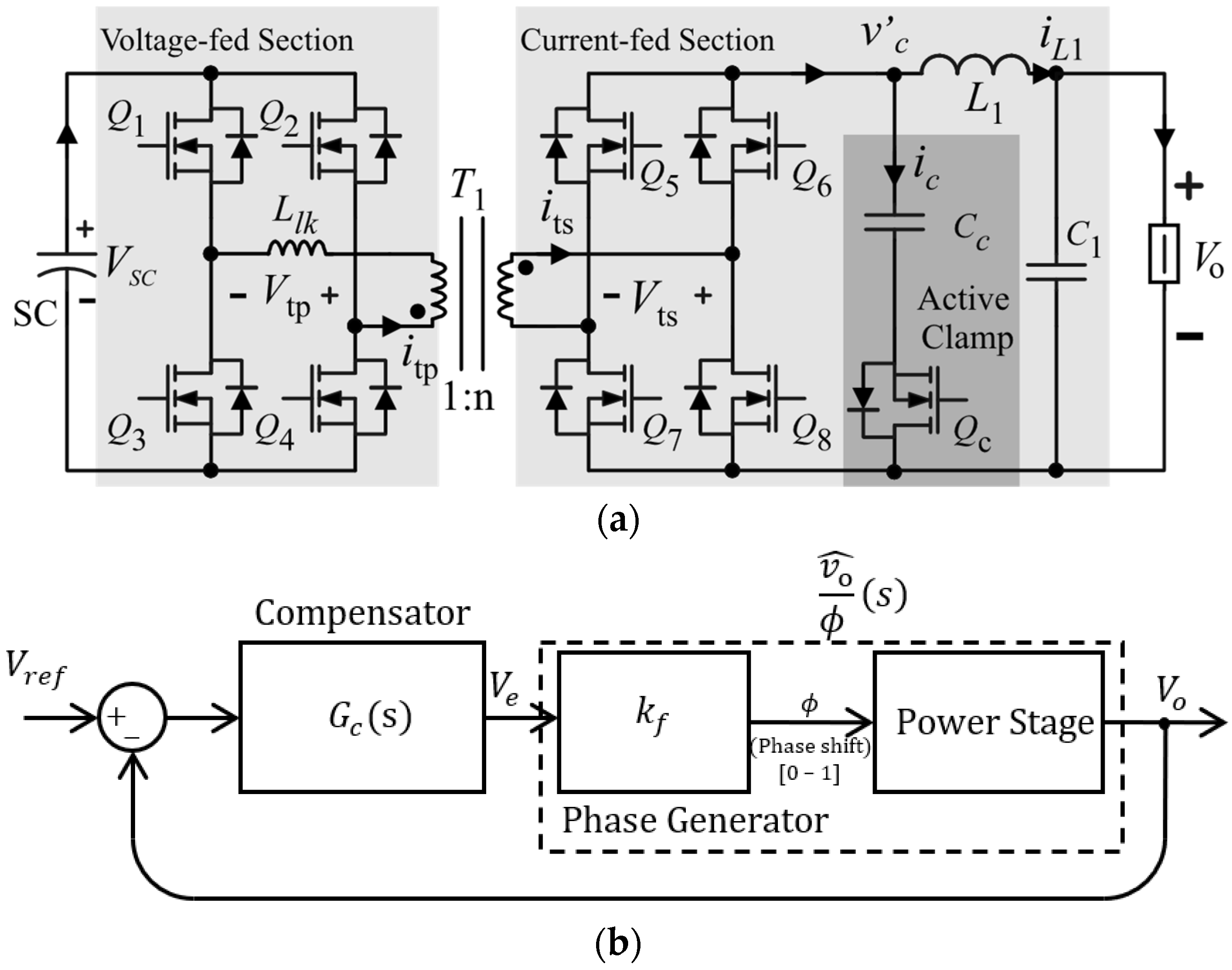
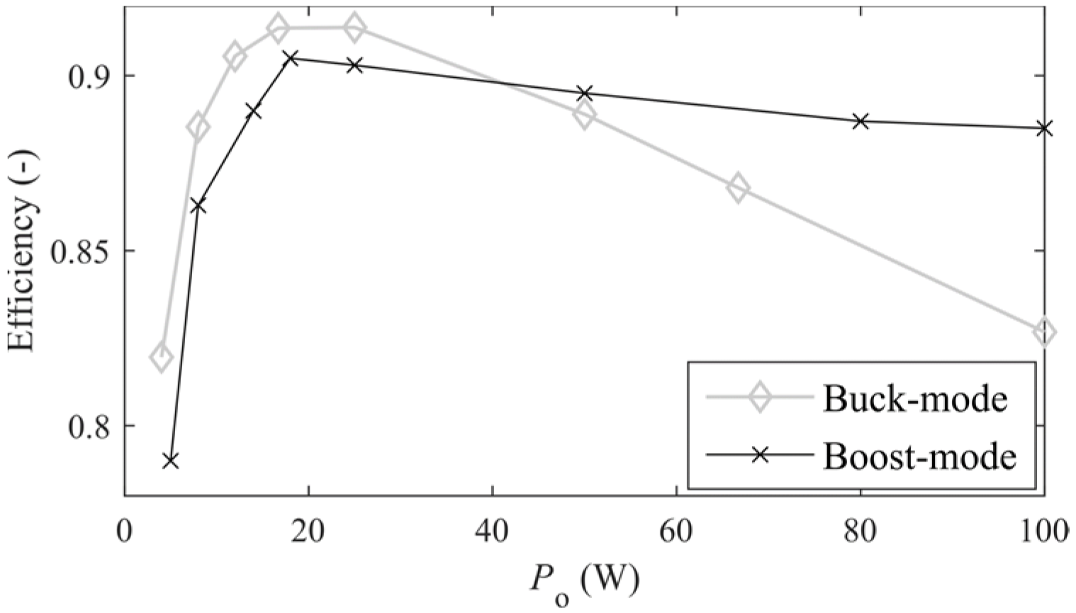
The DC/DC converter in the SM is a bidirectional full-bridge topology with an active clamp and a low pass filter (L1C1), as shown in Figure 3. This topology has ease of control and design as well as galvanic isolation. It allows bidirectional current flow from/to the SC ( V S C ) to/from the load (Vo). This converter offers soft-switching capabilities and uses synchronous rectification and an active clamp (Cc, Qc) to reduce the voltage stress in the switches. Figure 3a shows that the SC is attached to the 1st bridge (Q1 to Q4), isolation is provided by transformer T1, and Q5 to Q8 are used in the boost side (2nd bridge). This topology was first proposed in [27].

2.1. Buck-Mode ( V S C C → Vo)

The circuit can be analyzed by taking five-time intervals (from t1 to t6) in one half of a switching period ( T S ). The duty cycle for Q1, Q2, Q3, and Q4 is fixed at 50%, and the phase shift ( ϕ ) between legs Q1, Q3 and Q2, Q4 is the control variable.
The main buck-mode waveforms are presented in Figure 4. Before the first-time interval (before t 1 ), Q1 and Q2 are on, and Q3, Q4, and Qc are off. This means that the voltage in the transformer’s primary winding is zero (vtp = 0). The 2nd bridge (Q5Q8) is conducting at the same time. The diodes from Q5Q8 are on, and the synchronous rectifiers (Q5 and Q6) are working, so the transformer’s secondary voltage (vts) is zero and v c = 0, but V C c     V S C , where n is the transformer turn ratio. Therefore, there is no energy transfer from the primary to the secondary winding of the transformer. In addition, i L l k = 0 due to the previous cycle. The inductor current ( i L 1 ) flows through the 2nd bridge and through the load. As v c   = 0 and v C c > 0, i C c = 0 (diode of QC is blocking). This initial condition is the final condition in the last time interval of the previous half-cycle.
In the 1st time interval, [ t 1 , t 2 ], Q1, and Q4 are on, Q3 and Qc are off, and v L l k = V S C . As i L l k (t1) = 0, Q2 turns off at the zero current and Q4 also turns on at the zero current. L l k governs the current slope during the transition. Thus, both transitions occur during soft switching.
In the 2nd bridge, i L 1 is still flowing through the 2nd bridge diodes and synchronized rectifiers (Q5 and Q8), so v c = 0. This is equivalent to the off-time in the continuous mode for a buck converter, so the L1 current follows:
i L 1 ( t ) = i L 1 ( t 1 ) V o L 1 ( t t 1 ) ,
because v c = 0, this is valid from t1 to t2. i L l k continues to increase until the current in the secondary winding (its) reaches i L 1 and the diodes of Q6 and Q7 turn off. Therefore, for the 1st time interval, the i L l k current is governed by:
V S C = L l k d i L l k d t ,
which can be rewritten as:
i L l k = V S C L l k ( t t 1 ) .
The time interval ends when i L l k (t2) = i L 1 (t2). At that moment, the 2nd time interval starts [ t 2 , t 3 ]. Q2, Q3, and QC are still off and Q1 and Q4 are still on (so there are no switching transitions between the 1st and 2nd intervals). Q6 and Q7 and their diodes are already off, and Q5 and Q8 are on. The diode of QC starts conducting, so v c jumps to v C c (t2), which is a value that is slightly lower than V S C , resulting in CC being charged. The equations that govern the 2nd time interval are (considering Lmag >> L l k and n2 L l k << L1); for i L l k , we first subtract the charging voltage v c / n :
V S C v c n = L l k d i L l k d t ,
then i L 1 starts to increase following:
v c V o = L 1 d i L 1 d t ,
The charging current i C c is described by:
i C c = C c d v c d t ,  
Hence, the relationship between i l k ,   i C c ,   and i L 1 is:
i l k n i C c = i L 1 ,
Finally, the solution for i L 1 can be obtained:
i L 1 i L 1 ( t 2 ) + n · V S C V o L 1 ( t t 2 ) + L l k n 2 L 1 . V o . ( t t 2 ) n · V S C + L l k n 2 L 1 . V o v C c ( t 2 ) ω 0 L 1 s i n ( ω 0 ( t t 2 ) ) ,  
where the resonant frequency is ω 0 = [ C c n 2 L l k ] 1 . v c , iCc, and i L l k can be derived from (3) using (4). Notice that if n · V S C v C c ( t 2 ) is small, ω 0 ( t 3 t 2 ) < < 1 , and considering n 2 L l k L 1 ,   the last two terms of (4) can be neglected. Thus (4) is the same as in the on-time of a buck converter.
This time interval ends when Q1 is turned off and when the 3rd time interval, [ t 3 , t 4 ], starts. The i L l k flows through the diode of Q3 and Q4, and QC is on. Again considering ω 0 ( t 4 t 3 ) < <1):
i L 1 ( t ) i L 1 ( t 3 ) + v C c ( t 3 ) V o L 1 ( t t 3 ) .
As v C c ( t 3 ) n · V S C , (5) follows the on-state of a buck converter. CC delivers energy to reset L l k ( i L l k = 0). Then, Cc should have at least enough energy to reset L l k . This puts a lower limit on CC:
L L k i L k 2 ( t 3 ) 2 < C c ( v C c 2 ( t 3 ) v C c 2 ( t 4 ) ) 2 ,
which for design purposes is:
C C L L k I 0 max 2 V S C min 2 ,
where the low current ripple ( I o = i L l k (t3)/n) and v C c (t3) = V S C , and min and max are the maximum and minimum design values.
In the 4th time interval, [ t 4 , t 5 ], QC, Q4 are on but i L l k = 0, so the diode of Q3 is off, and CC is feeding L1. As this interval is short, ω 0 ( t 5 t 3 ) < < 1 , so the v c and i L 1 are:
v c ( t ) v c ( t 4 ) i L 1 ( t 4 ) C c ( t t 4 )
i L 1 ( t ) i L 1 ( t 4 ) + v c ( t 4 ) V o L 1 ( t t 4 ) .
Thus, if v c ( t 4 ) n · V S C , the buck converter equation remains. To achieve that, CC should be big enough to not be completely discharged by L l k , as proposed by (6).
In the 5th time interval, [ t 5 , t 6 ], QC is turned off, the diodes of Q5Q8 turn on, and right after that, Q7 turns on at zero voltage. Then, Q3 can turn on when the current and voltage are zero (soft switching). Thus, v c goes to zero, and i L 1 behaves as an off-time buck converter.
To summarize, the first-time interval is off-time, the second, third, and fourth are on-time intervals, and the fifth is an off-time interval. The voltage transfer function can be obtained as it was in the buck converter when v c ( t 2 ) v c ( t 3 ) v c ( t 4 ) v c ( t 5 ) = n V S C :
M = V o V S C n t 5 t 2 T S 2 n 2 ϕ
This mode is called buck-mode because M approximately follows the same equation as the buck converter; M varies linearly with the control variable ϕ , where controlling ϕ is sufficient to control the amount of energy that is transferred from the supercapacitor to the grid.
In order to control the SM, a small-signal analysis is performed. Let us simplify the time-interval analysis to only two main intervals. One from t2 to t5, where v c = n   · V S C , called on-state, and the other with the rest of the intervals, where v c = 0, which is called the off-state. The state model for the on-state is (t5t2) = ϕ TS:
d d t [ i L 1 v o ] = [ 0 1 / L 1 1 / C 1 1 / ( R C 1 ) ] × [ i L 1 v o ] + [ 1 / L 1 0 ] . n × v S C .
For the off-state, it is (1- ϕ )TS:
d d t [ i L 1 v o ] = [ 0 1 / L 1 1 / C 1 1 / ( R C 1 ) ] × [ i L 1 v o ] + [ 1 / L 1 0 ] .0 .
Therefore, using the averaging approach during TS/2, the complete model is obtained:
d d t [ i L 1 v o ] = [ 0 1 L 1 1 C 1 1 R C 1 ] × [ i L 1 v o ] + [ 1 L 1 0 ] .2 ϕ . n × v S C ,
where the < > represents the average in one switching period, and ϕ is shown in Figure 4. In addition, to obtain the small signal model, the variables are: x = X + x ^ , where X is the average value and x ^ is the small signal perturbation. Thus, the model in (11) becomes:
d d t [ I L 1 + i ^ L 1 V o + v ^ o ] = [ 0 1 L 1 1 C 1 1 R C 1 ] × [ I L 1 + i ^ L 1 V o + v ^ o ] + [ 2 L 1 0 ] . ( ϕ + ϕ ^ ) . n ( V S C + v ^ S C ) ,
then, by considering the perturbations on their own and by linearizing the model, the following expression can be obtained:
d d t [ i L 1 v ^ o ] = [ 0 1 L 1 1 C 1 1 R C 1 ] × [ i ^ L 1 v ^ o ] + [ 1 L 1 0 ] . n . ( ϕ . v ^ S C + V S C ϕ ^ ) ,
Finally, the Laplace transformation can be used as an output function of the control (control-to-output), and the input voltage can be obtained:
v o ^ ( s ) = n × ( ϕ × v ^ S C + V S C ϕ ^ ) s 2 L 1 C 1 + s L 1 R + 1 = n . ( ϕ × v ^ S C + V S C ϕ ^ ) ( s ω 0 ) 2 + s Q ω 0 + 1 .
Thus, based on the control-to-output transfer function, a controller must be selected in order to provide in the output a DC signal plus an AC 50 Hz signal. Therefore, a bandwidth of at least 500 Hz is needed for the SM in order to be considered as an ideal transfer function by a high-level controller, in this case the MMC main controller. A voltage mode controller was selected due to its simplicity, but a current mode controller can be utilized as well. To increase the bandwidth of the DC/DC converter a type-III controller was used with the following transfer function:
G C ( s ) = K ( s T + 1 ) s T × ( s α / ω c + 1 ) s α ω c + 1 × 1 s ω L P F + 1 ,
The type-III controller consists of a PI controller, defined by K and T, a lead-lag controller, defined by α and ω c ,   and a low pass filter with ω L P F   as the cut-off frequency. Therefore, the closed loop system to control the output voltage, according to Figure 3b, is:
G C l ( s ) = v o ^ v r e f ^ ( s ) = G C ( s ) v o ^ ϕ ^ ( s ) 1 + G C ( s ) v o ^ ϕ ^ ( s ) 1 1 + s Q ω f + s 2 ω f 2
In order to obtain that transfer function, the controller must have ω c = ω 0 . ( 1.1 ) , ω L P F = π f s   and α = 2.1 to have almost 50° of phase margin at around 10 kHz and K = 1.5 and T = 0.0005. This way, the MMC main controller will consider the SM with a simple transfer function and the control dynamics will not be coupled. Figure 5 shows the SM Bode plot with the described type-III controller and the MMC using a simple PI controller which is sufficient for a 50 Hz or 60 Hz sinusoidal output.

2.2. Boost-Mode (Vo V S C )

In this mode, energy is extracted from the grid and charges the SC. By controlling the boost voltage, it is possible to extract power from very low input voltage levels, such as those found in a sinusoidal wave close to the zero crossing. In this case, the active bridge is Q5Q8 and the synchronous rectifier bridge is Q1Q4. A complete analysis can be done using the same procedure as in the buck mode, here a simple analysis is presented only in order to obtain the voltage conversion ratio, based on the simulated waveforms of Figure 6. As in the buck mode, iL1 is triangular, it is charged when v c = 0 and discharged when v c n   · V S C . Thus, as L1 in this direction is in the “input” side (Vo) and v c reflects the “output” side ( V S C ), this behavior matches a boost converter with a voltage conversion ratio of:
M = V S C V o = T S / 2 ( t 3 t 1 ) . n T S 2 ( 1 D ) T S × n = 0.5 ( 1 D ) × n ,
where the time interval for transfer the energy to the “output” corresponds to the off-time of the boost converter, which is approximately t3t1, and the total time is T S /2 (converter’s energy transfer period is half of the sampling period). Finally, from Figure 6, t3t1 = ( 1 D ) T S / 2 . A more detailed analysis can be found in [28].

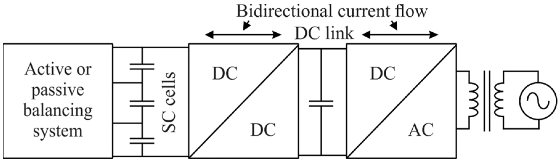
3. Modular Multilevel ESS

In the present work, only a single-phase converter is considered, but this can be extended to a three-phase system by repeating the structure. The proposed modular multilevel ESS is composed of SMs in series, which work as voltage sources, each of them including the DC/DC converter from Section 2 and an energy storage device (SC). This allows the discharge current to be perfectly controlled; this way, the SCs can be balanced using the same DC/DC converter. This section aims to show all of the functions of each submodule inside the MMC.

3.1. Energy Storage Device

The submodule includes the energy storage itself, so it is capable of delivering and absorbing energy using the SC. In this proposal, the energy storage device is a SC, but it can be replaced by a battery in EV applications or islanded microgrids with a high number of renewable sources.

3.2. DC/DC Conversion with Galvanic Isolation

The submodule includes an isolated DC/DC converter with a variable output voltage range. The converter’s output can fluctuate from values that are close to zero to positive values; in the present application, it goes from 1 V to 20 V (at VSC = 2.7 V). The module provides an AC output signal with a DC offset. Then, combining half of the SMs in one direction and the other half in the opposite direction, as shown in Figure 2b, the DC offset is cancelled, and a pure AC signal is obtained.
From the point of view of control, the MMC includes two control levels with two controllers: one controller inside each SM, which follows a voltage reference in the discharge direction (buck-mode) and a current reference in the charge direction (boost-mode), and one master controller, which measures the MMC’s output signals and controls the energy transfer to the grid or load. In addition, the SM controller performs the balancing of the SCs (detailed in Section 3.3) and establishes the protection limits.
In the discharge direction, see Figure 7, the SM measures the output voltage, the SC voltage, and current, and it controls the output voltage. The control loop is based on a type-III controller, which was designed in Section 2.
In the charge direction, see Figure 8, the DC/DC controls the SC current and keeps the SC voltage within the limits. The type-III controller is limited when the voltage of the SC is approaching its maximum. The comparator creates the PWM signals and the T S / 2 delay, and the NOR gate creates the switching pulses.

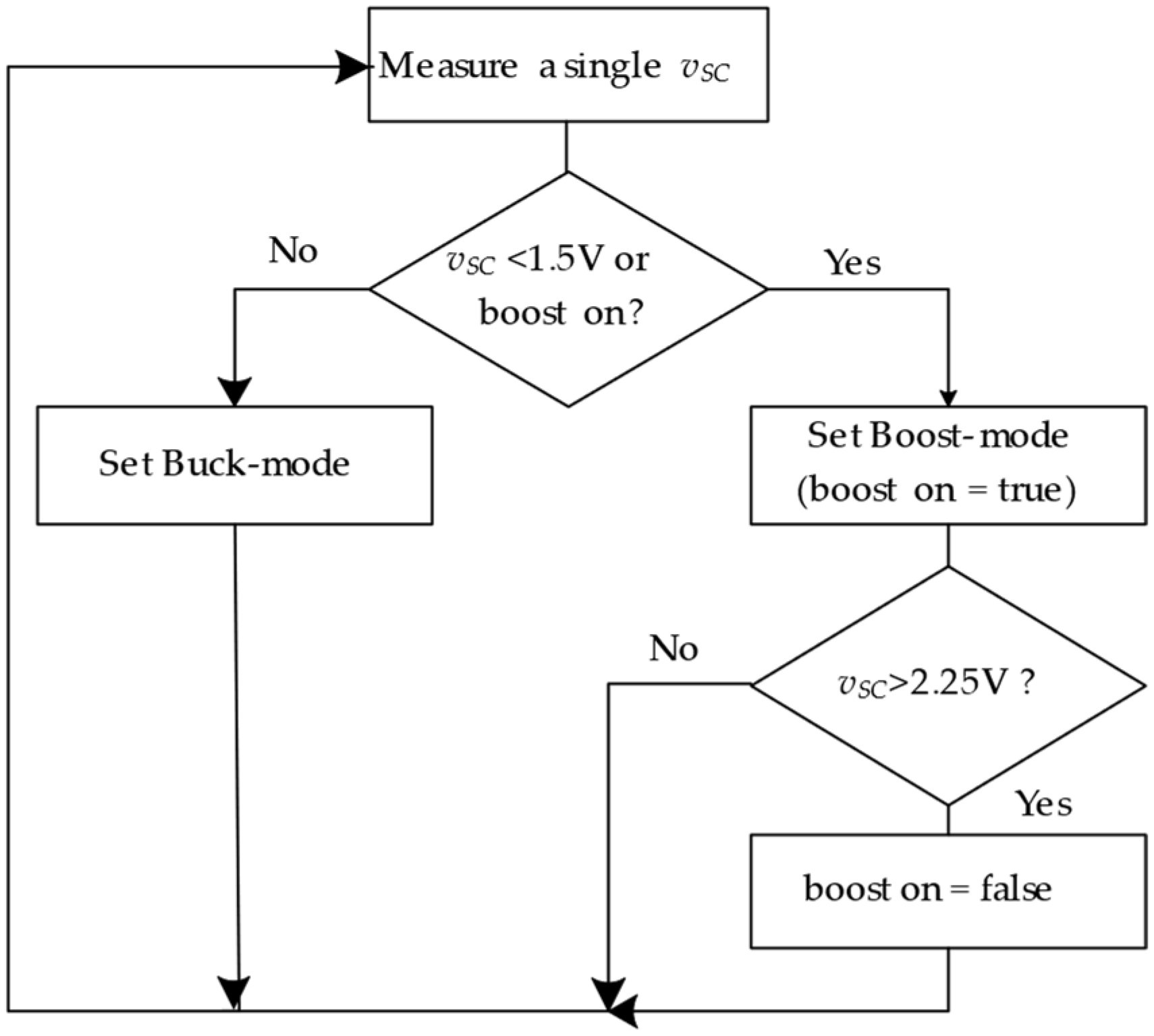
3.3. Balancing Method

In order to simplify the control of the whole MMC and to add minimal circuitry to sense and control the SMs, the balancing of the SCs is conducted locally in each SM instead of giving this task to the master controller. Therefore, many SMs can be connected in series without increasing complexity in the control algorithm, as self-balancing is achieved at the SM level.
At hardware level (see Section 5), each SM is composed of a Microcontroller Unit (MCU) and all of the components that are required for operation. By taking advantages of this MCU, an integrated control can be implemented in such a way that the output power can be slightly adjusted for each SM in order to increase or decrease it. Thus, The SCs can be balanced without recirculating energy from one another. This is the main benefit of the proposed balancing control since any other active balancing system relies on the need to transfer the exceeding energy to another SC, and if the system is simple, then this energy might not be directly injected to the lowest voltage SC cell [4].
SCs are balanced when working in the buck-mode. Each SM measures its own SC voltage ( V S C n ) and two adjacent SC voltages ( V S C n 1 and V S C n + 1 ), as shown in Figure 9. Thus, the DC/DC converter controller checks whether the SC is over or under the average voltage of this local measurement.
An error signal is defined as:
ε = 3 × V S C n V S C n + 1 + V S C n + V S C n 1 1 ,
Finally, the reference for the output voltage of the n-th SM is:
V R E F n = V R E F + V R E F K ε v n ,
where K is the proportional gain to limit v n to around 10% of the reference value V R E F . This means that v n can be slightly higher or lower than zero, and it is then added to V R E F , generating an individual V R E F n = V R E F + v n for the n-th SM. As each SM controller is based on an MCU, these calculations are included in the SMs, as illustrated in Figure 9. In the boost-mode, the same method can be used if i n is added to I R E F .

3.4. DC/AC Conversion

Figure 2b shows two branches of SMs, the top and the bottom. The top branch delivers the positive half sinewave, and the bottom branch delivers the negative half sinewave. The master controller needs to sense the output voltage and current of the MMC (vMMC and iMMC) to properly command the whole array of SMs by sending only two variables to each SM: the operation mode (buck or boost-mode) and V R E F (for buck-mode) or I R E F (for boost-mode). These signals are sent to every SM in the corresponding active branch.
The master controller combines two 180° sinusoidal signals to achieve the DC/AC conversion. Figure 10 shows the controller details. In the proposed approach, the dq-frame method was used. The phase-locked loop (PLL) block obtains the grid angle and frequency [29] in order to extract the DC component to a low pass filter using a cut-off frequency of 5 Hz. The dq block includes the low pass filter, the DC signal, and the orthogonal signals, so its outputs are the dq signals and the DC component: dq0 signals.
The main controller shown in Figure 10a consists of three PI controllers: two of them for the dq components and one more to minimize the DC value and the cross idiq coupling elements (see Figure 10b). The resultant signal is processed and is divided by the number of SMs and is shifted by 180° to provide the signals to the lower half of the SMs. In order to clarify the control loop and to design the controller parameters, the d-axis control loop is shown Figure 10b. The PI values can be obtained by cancelling the rC–LC pole with the PI zero at −1/τ and by finally selecting K in order to provide stability and decent bandwidth. For this case, K/(rC·τ) = ω 0 / 10 was selected, where ω0 was 2·π·10 kHz.

3.5. Grid Connection with Bidirectional Power Flow

As the converter can work in buck or boost-mode, Figure 11 shows a flow diagram that explains how the mode selector works. To absorb power, the DC/DC converter in each SM can operate in boost or buck-mode. In boost-mode, an IREF signal is used to control the amount of power that is absorbed from the grid. It is preferable for only active power to be absorbed when working in the boost-mode, mainly because the losses can be higher when reactive power is being absorbed.
The mode selector retrieves the SC voltage from any SM (since all of them should be balanced automatically) and checks whether the voltage is lower than a predefined value (1.5 V in this case). If so, the boost-mode is activated to absorb active power from the grid and to recharge the SCs. This voltage level was selected to charge the SCs when they are close to their lowest limit and when they can no longer deliver energy in the buck-mode. After charging the SCs and once they reach a valid working level (2.25 V), the master controller selects the buck-mode. The buck-mode works in a voltage-controlled scheme, where the controller supervises vMMC and iMMC (Figure 7 and Figure 10) and where each SM can deliver or absorb active or reactive power by controlling id or iq.
Since the proposed ESS is based on a series chain of DC/DC converters, it can also be used in DC microgrids, and as mentioned before, if batteries are the primary energy storage device, then a different control strategy can be used [30,31]. The present work is limited to demonstrating the capabilities of the proposed ESS, and more advanced control techniques should be addressed in future work.

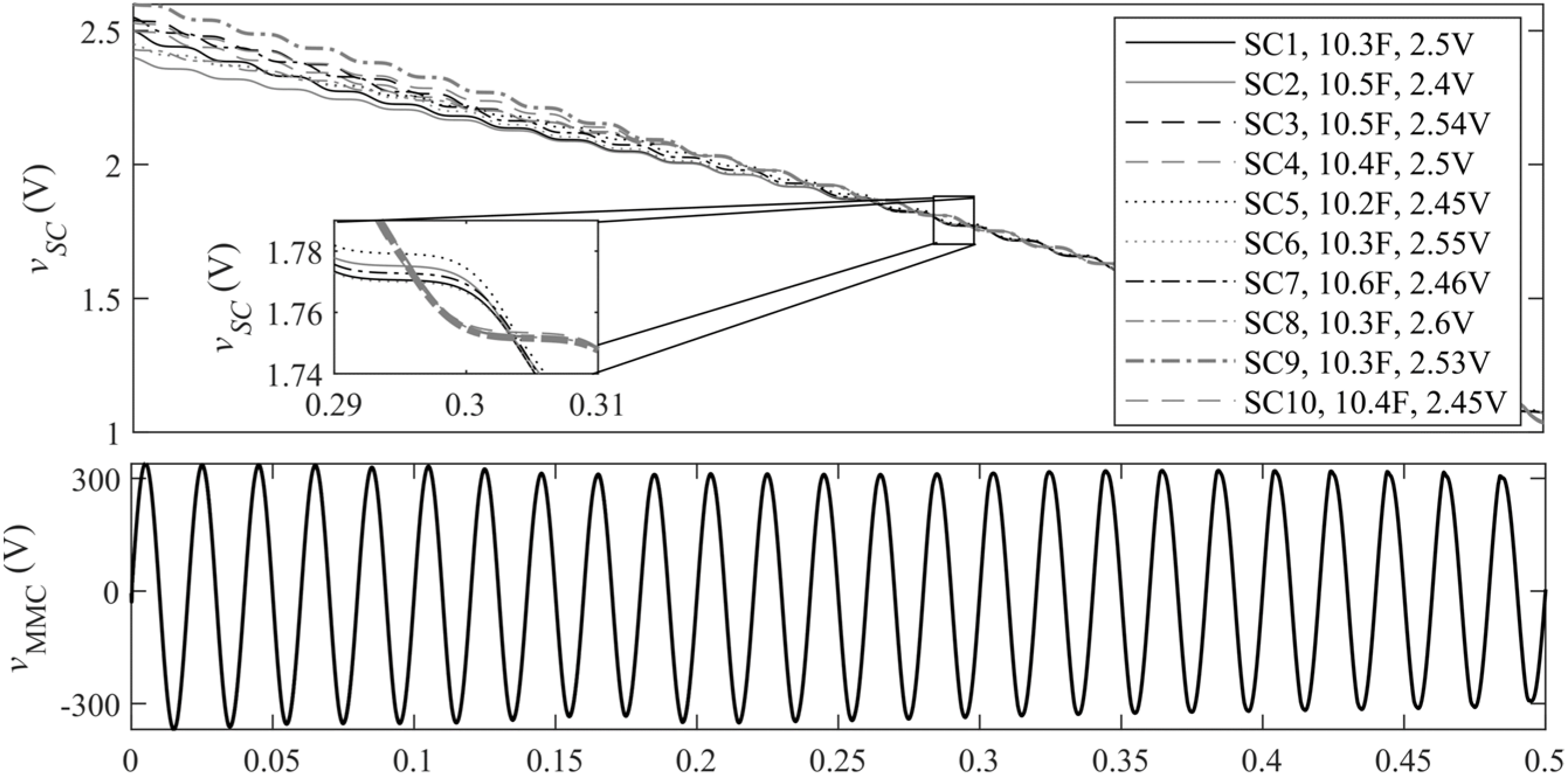
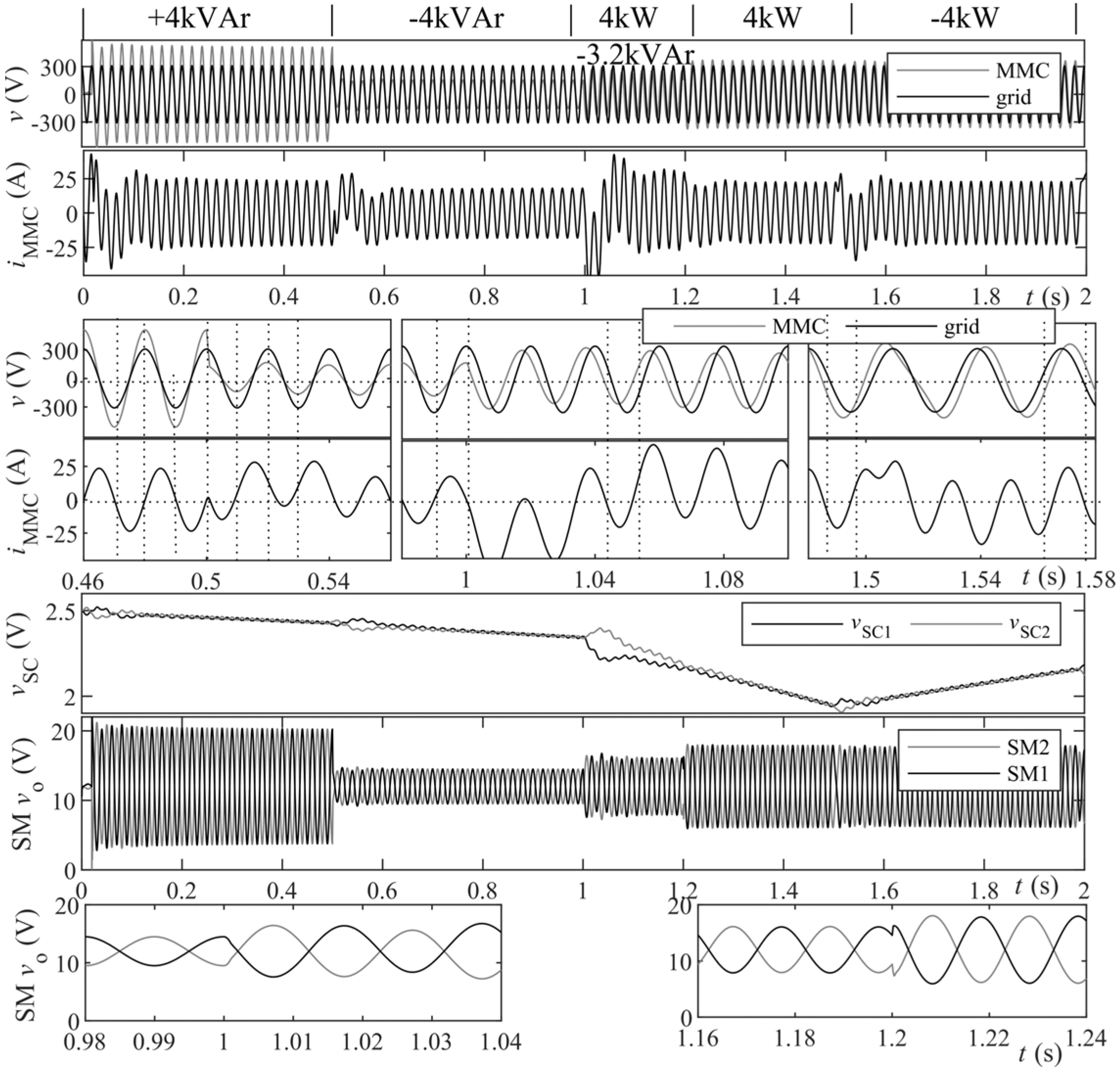
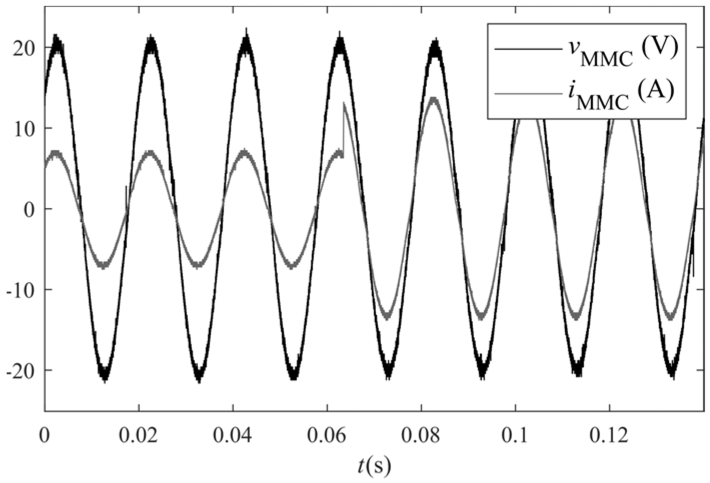
4. Simulation Results

The ESS design was validated using a PSIM simulator. Four simulations were performed for a total of 62 SMs (31 SMs for each branch, top and bottom) to obtain an output voltage of 220VAC at 50 Hz. Table 1 shows the components for each SM and the coupling inductor (LC). To reduce the simulation time, a SC with a capacitance value of 10F was used if not specified in the figure.
The first simulation was performed to validate the DC/DC converter that was delivering a DC signal. The waveforms in Figure 4 correspond to a simulation of the converter with V R E F   = 5 V in the buck-mode, which was used during converter analysis.
The second simulation consisted of a discharge process with a forced unbalanced condition in the SC voltages to verify the self-balancing algorithm that was working in the buck-mode. To that end, the capacitance and the initial voltage values of the SCs were set to be slightly different. The converter was commanded to deliver 10.2 kW to a resistive–inductive load (4.9 Ω-7 mH). The initial voltage difference between the ten plotted SC voltages (of the 62 SCs in the whole chain) was 200 mV. Figure 12 shows the voltage of these ten SCs, including the initial voltage and capacitance. Notice that around 0.3 s after the discharging process started, the voltage difference between the maximum and minimum values was reduced to 10mV, which is small enough to consider the SCs to be balanced. In the MMC, the upper half modules have a different voltage than the bottom half modules, as the zoom in Figure 12 shows. This is because the energy is transferred from the upper half modules during the positive half cycle and from the bottom half modules during the negative half cycle. Thus, the upper and the bottom half modules are balanced (voltage difference less than 10 mV) at different voltages, but both groups are close, around 20 mV for the 10F case.
Although the SCs were initially unbalanced, vMMC stayed stable for the whole time that the algorithm presented in Section 3.3 was balancing the SCs. This test also validates AC operation using the MMC configuration and the wide input operating voltage range of each SM, from 2.7 V to 1.0 V, where vMMC is slightly reduced when the SC voltage is lower than 1.5 V.
The third simulation consisted of connecting the MMC to the grid to validate the operations of the four quadrants involved in the buck-mode. Figure 13 demonstrates the capabilities of the MMC under different MMC voltage angles and amplitudes. In the simulations, the angles and amplitudes were controlled by IREF_dq. Thus, different power transfers could be obtained. This simulation was created using the controller proposed in Figure 10. Figure 13 shows the voltage in two SMs from different half branches (top and bottom), iMMC and vMMC. In the first interval, the MMC delivers 4 kVAr of reactive power with IREF_dq = (IREF_d, IREF_q) = (0, 25 A). Then, the MMC absorbs 4 kVAr, so IREF_dq = (0, −25 A). Then, at t=1s, active power is delivered, so for 0.2 s, the system delivers 4kW-3.2kVAr, IREF_dq = (25 A, −20 A). After that, the reactive current is set to zero, and only active power is delivered. Finally, 4 kW of active power is absorbed. This test shows the MMC is capable of absorbing and delivering active and reactive power. Notice the balancing process in the SC voltages and the increase and decrease in the SC voltages when they are absorbing and delivering power, respectively.
The fourth simulation validated the boost-mode (or absorbing mode), as shown In Figure 14, where the SC in each SM recharges from 1.4 V to 2.25 V and where the SCs are balanced at the same time.

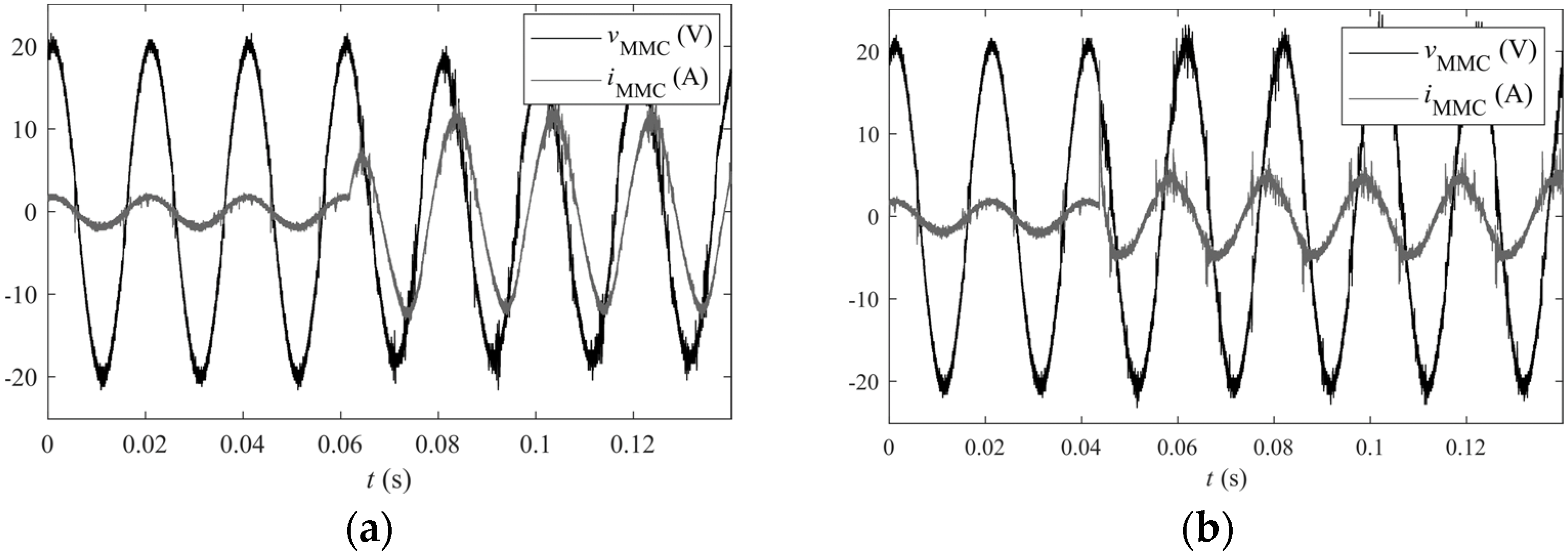
5. Experimental Results

A down-scaled prototype for two SMs from each half branch was constructed, with a maximum power transfer of 175W per SM. Figure 15 shows the complete MMC, which is composed of the top branch, the bottom branch, a vMMC and iMMC sensor board, and a microcontroller unit (MCU), which acts as the master controller. Each SM integrates all of the components that are listed in Table 1; the power switches are at the bottom and are attached to a heatsink. In addition, the TI TMS320F28027 DSP was used as the SM controller, which includes the proportional controller for balancing the SCs and the PWM generator. The SM planar transformer was designed and developed specifically for the prototype. The master controller was implemented in a TI TMS320F28379D MCU, which gives the references to the SMs.
Three experimental tests were performed. The first test was the validation of the SM waveforms in buck-mode and boost-mode, as shown in Figure 16. These waveforms are consistent with the theoretical and simulated ones (Figure 4 and Figure 5).
The second test shows the operation of the MMC. Figure 17 shows the discharge mode (buck-mode) with a resistive load; the test depicts vMMC and iMMC. It shows that the voltage stayed stable during a step change in the load.
The third test shows the operation of the MMC when the load changes from R to RL and from R to RC, as shown in Figure 18, which validates the operation with reactive current flow. As the grid connection was validated in the simulation section, only the MMC was tested with different experimental loads to generate the experimental results, and thus the MMC was the only AC grid generator.
Finally, the fourth test demonstrated the efficiency of the whole MMC in both operation modes, as shown in Figure 19. The efficiency at high power is not as good as it is in a high-voltage DC/DC converter because of the large currents and low input voltages; however, it can be improved by paralleling the DC/DC converters in each submodule and by using wide band semiconductors, such as GaN or SiC. The prototype shows how the circuit works; however, the efficiency is not optimized and can be improved further.

Comparsion with Other ESSs

In order to summarize the advantages and disadvantages of the proposed converter, Table 2 is presented. To make a fair comparison between the proposed ESS, only systems that require one additional stage to operate in the same way as the one proposed here are analysed.
The converter that is proposed in [17] requires an additional balancing system for the SC cells but provides isolation and the DC/DC and DC/AC conversions in a single cell. The main drawback is that the efficiency is not as high as the proposed converter.
A highly efficient multi-cell converter is presented in [18]; however, a balancing system is required in order to accommodate the SC cells. However, the complexity of the converter’s transformer design and control operation can be the main drawbacks, and the high efficiency can be reduced with the incorporation of the balancing system.
A comparable ESS is presented in [25] since it is based on the traditional control scheme of MMC. A high THD is presented at the output, but because of this, the efficiency is high due the fact that less switching stress is presented. However, this ESS lacks isolation, and if required, a bulky transformer should be placed at the output and efficiency could be further reduced.
Since the proposed ESS can accomplish all of the required stages in a single SM and since the balancing control is embedded and is relatively simple to operate, the main concern relays in the efficiency of the system. For this reason, the only drawback would be the cost if efficiency has to be increased, as GaN or SiC transistors should be integrated in each SM.

6. Conclusions

In a traditional supercapacitor (SC)-based ESS, four stages are needed: energy storage devices, the balancing system, and the DC/DC and DC/AC converters that connect the storage devices to the grid. The SC-based ESS that is proposed in this article uses a modular multilevel converter (MMC) that is able to reduce the number of stages by performing the self-balancing process and the DC/DC and DC/AC conversions in a single stage. Each submodule (SM) of the MMC consists of a DC/DC converter and a single SC. The DC/DC converter is a bidirectional full-bridge that has an active clamp and soft-switching techniques and works at 100 kHz and at low input voltages. In addition, the DC/DC converter includes a planar transformer, galvanic isolation is also achieved, and a bulky 50 Hz transformer can be avoided.
The MMC that was proposed here can be implemented using a large number of SMs in series without increasing the complexity of the main controller. This is because the balancing process is performed in each SM, and the main controller only governs the power flow between the SCs and the grid. This makes the proposed MMC attractive for SC-based ESS designs.
The proposed design was validated in simulations and in a real prototype. Four-quadrant operation with low distortion was achieved. Although the efficiency was not greater than those of the compared topologies, further work should overcome this limitation by using GaN or SiC transistors.

Author Contributions

Conceptualization, F.D.H. and F.M.I.; methodology, F.M.I.; software, F.D.H. and R.S.; validation, F.D.H., F.M.I. and F.M.; formal analysis, R.S.; investigation, F.D.H.; resources, F.M.I.; data curation, R.S.; writing—original draft preparation, F.D.H.; writing—review and editing, F.D.H., F.M.I. and F.M.; visualization, F.D.H.; supervision, F.M.I.; project administration, F.M.I.; funding acquisition, F.M.I. All authors have read and agreed to the published version of the manuscript.

Funding

This work was carried out as a part of the AMPaC Megagrant project supported by The Ministry of Education and Science of Russian Federation, Grant Agreement No 075-10-2021-067, Grant identification code 000000S707521QJX0002.

Institutional Review Board Statement

Not applicable.

Informed Consent Statement

Not applicable.

Data Availability Statement

Not applicable.

Acknowledgments

The authors would like to thank W. Baldwin for the great help.

Conflicts of Interest

The authors declare no conflict of interest.

Abbreviations

ESSEnergy storage system
MMCModular multilevel converter
SMSubmodule
SCSupercapacitor
THDTotal harmonic distortion
MCUMicrocontroller unit

Nomenclature

vMMCOutput voltage port of the MMC
LCCoupling inductor
vgridGrid voltage
L1Output inductor at SM level
C1Output capacitor at SM level
VSCSupercapacitor voltage at SM level
VoOutput voltage at SM level
CcClamp capacitor at SM level
QcClamp switch at SM level
Q1 to Q4Full-bridge voltage-fed section switches at SM level
T1High-frequency transformer at SM level.
Q5 to Q8Full-bridge current-fed section switches at SM level.
t1 to t6time intervals for the DC/DC converter operation
T S Switching period
ϕ Phase-shift angle
D Duty cycle at boost-mode
L l k Leakage inductance
LmagMagnetizing inductance
vtpTransformer’s primary voltage
vtsTransformer’s secondary voltage
v c Clamp voltage node
nTransformer’s turn-ratio
V C c Clamp capacitor’s voltage
i L l k Leakage inductor’s current
i L 1 Output inductor’s current
i C c Clamp capacitor’s current
v L l k Leakage inductor’s voltage
ω 0 Resonant frequency between the capacitor’s clamp and the leakage inductance
IoOutput current at SM level
MVoltage transfer function at SM level
f s Switching frequency
G C Type-III controller transfer function at SM level
α Lead-lag alfa parameter of the type-III controller
K Gain parameter of the type-III controller
TTime constant of the type-III controller
ω c Lead-lag frequency parameter of the type-III controller
ω L P F Low pass filter frequency of the type-III controller
ε Error signal for the supercapacitor balancing embedded controller at each SM
V R E F Voltage reference for each SM at MMC level
i R E F Current reference for each SM at MMC level
i MMC MMC current

References

  1. Farhadi, M.; Mohammed, O. Energy Storage Technologies for High-Power Applications. IEEE Trans. Ind. Appl. 2016, 52, 1953–1962. [Google Scholar] [CrossRef]
  2. Khaligh, A.; Li, Z. Battery, Ultracapacitor, Fuel Cell, and Hybrid Energy Storage Systems for Electric, Hybrid Electric, Fuel Cell, and Plug-in Hybrid Electric Vehicles: State of the Art. IEEE Trans. Veh. Technol. 2010, 59, 2806–2814. [Google Scholar] [CrossRef]
  3. Kotz, R.; Carlen, M. Principles and Applications of Electrochemical Capacitors. Electrochim. Acta 2000, 45, 2483–2498. [Google Scholar] [CrossRef]
  4. Ibanez, F.; Vadillo, J.; Echeverria, J.M.; Fontan, L. Design Methodology of a Balancing Network for Supercapacitors. In Proceedings of the 2013 4th IEEE/PES Innovative Smart Grid Technologies Europe (ISGT Europe 2013), Lyngby, Denmark, 6–9 October 2013; Volume 2, pp. 1–5. [Google Scholar]
  5. Li, L.; Huang, Z.; Li, H.; Peng, J. A Rapid Cell Voltage Balancing Scheme for Supercapacitor Based Energy Storage Systems for Urban Rail Vehicles. Electr. Power Syst. Res. 2017, 142, 329–340. [Google Scholar] [CrossRef]
  6. Falck, J.; Felgemacher, C.; Rojko, A.; Liserre, M.; Zacharias, P. Reliability of Power Electronic Systems. IEEE Ind. Electron. Mag. 2018, 12, 24–35. [Google Scholar] [CrossRef] [Green Version]
  7. Yang, S.; Bryant, A.; Mawby, P.; Xiang, D.; Ran, L.; Tavner, P. An Industry-Based Survey of Reliability in Power Electronic Converters. IEEE Trans. Ind. Appl. 2011, 47, 1441–1451. [Google Scholar] [CrossRef]
  8. Lone, S.A.; Iqbal, S.J.; Ahmad, M.; Ismail, M. Super-Capacitor Based Energy Storage System for Improved Load Frequency Control. Electr. Power Syst. Res. 2009, 79, 226–233. [Google Scholar]
  9. Partridge, J.; Abouelamaimen, D.I. The Role of Supercapacitors in Regenerative Braking Systems. Energies 2019, 12, 2683. [Google Scholar] [CrossRef] [Green Version]
  10. Kerdphol, T.; Rahman, F.S.; Watanabe, M.; Mitani, Y. Robust Virtual Inertia Control of a Low Inertia Microgrid Considering Frequency Measurement Effects. IEEE Access 2019, 7, 57550–57560. [Google Scholar] [CrossRef]
  11. Khalid, M. A Review on the Selected Applications of Battery-Supercapacitor Hybrid Energy Storage Systems for Microgrids. Energies 2019, 12, 4559. [Google Scholar] [CrossRef] [Green Version]
  12. Ibañez, F.M.; Vadillo, J.; Echeverria, J.M.; Fontán, L. 100 kW Bidirectional DC/DC Converter for a Supercapacitor Stack. In Proceedings of the 2013 4th IEEE/PES Innovative Smart Grid Technologies Europe (ISGT Europe 2013), Lyngby, Denmark, 6–9 October 2013; pp. 1–5. [Google Scholar]
  13. Ibanez, F.M.; Echeverria, J.M.; Vadillo, J.; Fontan, L. Multimode Step-up Bidirectional Series Resonant DC/DC Converter Using Continuous Current Mode. IEEE Trans. Power Electron. 2015, 30, 1393–1402. [Google Scholar] [CrossRef]
  14. Luna, M.; Sferlazza, A.; Accetta, A.; Di Piazza, M.C.; La Tona, G.; Pucci, M. Modeling and Performance Assessment of the Split-Pi Used as a Storage Converter in All the Possible DC Microgrid Scenarios. Part I: Theoretical Analysis. Energies 2021, 14, 4902. [Google Scholar] [CrossRef]
  15. Luna, M.; Sferlazza, A.; Accetta, A.; Di Piazza, M.C.; La Tona, G.; Pucci, M. Modeling and Performance Assessment of the Split-Pi Used as a Storage Converter in All the Possible DC Microgrid Scenarios. Part II: Simulation and Experimental Results. Energies 2021, 14, 5616. [Google Scholar] [CrossRef]
  16. Wang, L.; Guo, J.; Xu, C.; Wu, T.; Lin, H. Article Hybrid Model Predictive Control Strategy of Supercapacitor Energy Storage System Based on Double Active Bridge. Energies 2019, 12, 2134. [Google Scholar] [CrossRef] [Green Version]
  17. Ibanez, F.M. Bidirectional Series Resonant DC/AC Converter for Energy Storage Systems. IEEE Trans. Power Electron. 2019, 34, 3429–3444. [Google Scholar] [CrossRef]
  18. Ertl, H.; Kolar, J.W.; Zach, F.C. A Novel Multicell DC-AC Converter for Applications in Renewable Energy Systems. IEEE Trans. Ind. Electron. 2002, 49, 1048–1057. [Google Scholar] [CrossRef]
  19. Allebrod, S.; Hamerski, R.; Marquardt, R. New Transformerless, Scalable Modular Multilevel Converters for HVDC-Transmission. In Proceedings of the 2008 IEEE Power Electronics Specialists Conference, Rhodes, Greece, 15–19 June 2008; pp. 174–179. [Google Scholar]
  20. Ferreira, J.A. The Multilevel Modular DC Converter. IEEE Trans. Power Electron. 2013, 28, 4460–4465. [Google Scholar] [CrossRef]
  21. Ibanez, F. Quasi-Resonant Multilevel Converter for Supercapacitor Energy Storage Systems. In Proceedings of the 2017 IEEE PES Innovative Smart Grid Technologies Conference Europe (ISGT-Europe), Turin, Italy, 26–29 September 2017; pp. 1–6. [Google Scholar]
  22. Mukherjee, N.; Tricoli, P. Modular Multilevel Converter Based Supercapacitor Integration Strategies and Their Comparative Evaluation for Railway Traction Drive Systems. In Proceedings of the 2015 17th European Conference on Power Electronics and Applications (EPE’15 ECCE-Europe), Geneva, Switzerland, 8–10 September 2015; pp. 1–10. [Google Scholar]
  23. Hernandez, F.D.; Ibanez, F.; Samanbakhsh, R.; Velazquez, R. A Comparative Study of Energy Storage Systems Based on Modular Multilevel Converters. In Proceedings of the IECON 2021—47th Annual Conference of the IEEE Industrial Electronics Society, Toronto, ON, Canada, 13–16 October 2021; pp. 1–5. [Google Scholar]
  24. Errigo, F.; Venet, P.; Chedot, L.; Sari, A. Optimal Supercapacitor Pack Sizing for Modular Multilevel Converter with Integrated Energy Storage System. In Proceedings of the 2018 IEEE International Conference on Industrial Technology (ICIT), Lyon, France, 20–22 February 2018; pp. 1760–1766. [Google Scholar]
  25. Coppola, M.; Del Pizzo, A.; Iannuzzi, D. A Power Traction Converter Based on Modular Multilevel Architecture Integrated with Energy Storage Devices. In Proceedings of the 2012 Electrical Systems for Aircraft, Railway and Ship Propulsion, Bologna, Italy, 16–18 October 2012; pp. 1–7. [Google Scholar]
  26. Montesinos-Miracle, D.; Massot-Campos, M.; Bergas-Jane, J.; Galceran-Arellano, S.; Rufer, A. Design and Control of a Modular Multilevel DC/DC Converter for Regenerative Applications. IEEE Trans. Power Electron. 2013, 28, 3970–3979. [Google Scholar] [CrossRef]
  27. Wang, K.; Lee, F.C.; Lai, J. Operation Principles of Bi-Directional Full-Bridge DC/DC Converter with Unified Soft-Switching Scheme and Soft-Starting Capability. In Proceedings of the Fifteenth Annual IEEE Applied Power Electronics Conference and Exposition (Cat. No.00CH37058), New Orleans, LA, USA, 6–10 February 2002; pp. 111–118. [Google Scholar]
  28. Prasanna, U.R.; Rathore, A.K. Extended Range ZVS Active-Clamped Current-Fed Full-Bridge Isolated DC/DC Converter for Fuel Cell Applications: Analysis, Design, and Experimental Results. IEEE Trans. Ind. Electron. 2013, 60, 2661–2672. [Google Scholar]
  29. Freijedo, F.D.; Doval-Gandoy, J.; Lopez, O.; Cabaleiro, J. Robust Phase Locked Loops Optimized for DSP Implementation in Power Quality Applications. In Proceedings of the 2008 34th Annual Conference of IEEE Industrial Electronics, Orlando, FL, USA, 10–13 November 2008; pp. 3052–3057. [Google Scholar]
  30. Qin, Y.; Hua, H.; Cao, J. Stochastic Optimal Control Scheme for Battery Lifetime Extension in Islanded Microgrid via a Novel Modeling Approach. IEEE Trans. Smart Grid 2019, 10, 4467–4475. [Google Scholar] [CrossRef]
  31. Hua, H.; Qin, Y.; Cao, J. Coordinated Frequency Control for Multiple Microgrids in Energy Internet: A Stochastic H∞ Approach. In Proceedings of the 2018 IEEE Innovative Smart Grid Technologies—Asia (ISGT Asia), Singapore, 22–25 May 2018; pp. 810–815. [Google Scholar]
Figure 1. Traditional SC-based ESS block diagram; arrows indicate bidirectional current flow.
Energies 15 00338 g001
Figure 2. Block diagram for (a) traditional and (b) proposed MMC topology.
Energies 15 00338 g002
Figure 3. Submodule: (a) bidirectional full-bridge circuit, (b) inner control loop.
Energies 15 00338 g003
Figure 4. Buck-mode waveforms.
Energies 15 00338 g004
Figure 5. Closed loop transfer function for: (a) SM using a type-III controller and (b) MMC using a PI controller.
Energies 15 00338 g005
Figure 6. Boost-mode waveforms.
Energies 15 00338 g006
Figure 7. Buck-mode Controller.
Energies 15 00338 g007
Figure 8. Boost-mode controller.
Energies 15 00338 g008
Figure 9. Balancing control integrated in each SM to achieve self-balancing.
Energies 15 00338 g009
Figure 10. MMC controller (a) general scheme, (b) detail of d-component loop.
Energies 15 00338 g010
Figure 11. Mode selector diagram.
Energies 15 00338 g011
Figure 12. Balancing process (10 kW, discharge mode) in the whole voltage range.
Energies 15 00338 g012
Figure 13. Delivering or absorbing active or reactive power in buck-mode with zoomed sections.
Energies 15 00338 g013
Figure 14. Boost-mode recharging the SCs.
Energies 15 00338 g014
Figure 15. Complete MMC prototype.
Energies 15 00338 g015
Figure 16. Experimental waveforms for each SM in (a) buck and (b) boost-mode.
Energies 15 00338 g016
Figure 17. MMC output voltage and current for a step change in the load.
Energies 15 00338 g017
Figure 18. Step response from (a) R to RL and (b) R to RC.
Energies 15 00338 g018
Figure 19. Efficiency of a single SM for the Buck-mode and Boost-mode.
Energies 15 00338 g019
Table 1. Components used for simulation and prototype tests.
ComponentValueDetails
SC10F PSIM and 3000F prototypeESR = 0.4 mΩ
Q1 to Q43 × BSC009NE2LS5rDS(on) = 0.9 mΩ
Q5 to Q8 and Qc2 × BSC022N04LS6rDS(on) = 2.2 mΩ
T1 core and LMAG5.7 µHELP32, N87 material
Turns ratio1:8-
CC6 × 0.068 µF in parallel0805 X7R
L110 µHEPCOS B82559
C12 × 100 µF in parallelSolid tantalum
TS10 µS1/TS = Fsw = 100 kHz
LC1 mHCoupling inductor
Table 2. Components used for simulations and prototype’s tests.
ESSEfficiency
at 50%
Additional
Stages
Drawbacks
[17]84~86%Balancing systemMedium THD
[18]95~97%Balancing systemComplexity
[25]91~94% *Output transformerHigh THD
Proposed85~88%NoneCost
* Obtained by numerical simulations.
Publisher’s Note: MDPI stays neutral with regard to jurisdictional claims in published maps and institutional affiliations.

