1. Introduction
In recent years, a large amount of literature has emerged on the topic of achieving high efficiency in a wide operation range due to the urgent needs of complex applications, such as renewable energy generation, hybrid electric vehicles, and undersea cabled observatories [
1,
2]. On the other hand, special requirements, such as low current ripple, would be crucial technical indicators for undersea cabled observatories because the current ripple may greatly affect the service life of equipment [
3,
4]. Therefore, wide-voltage-gain DC/DC converters with low current ripple and high-power density have become an indispensable part of such applications in order to realize the subsea source interface.
The LLC resonant converter has been paid much attention because of its zero-voltage switching (ZVS) of main switches, wide operation range, low electromagnetic interference, and high-power density [
5,
6,
7,
8,
9,
10]. Normally, the switching frequency range needs to be expanded to achieve a wide operation range when the traditional frequency modulation (FM) is applied to the LLC resonant converter. Then, the ZVS is hard to realize under light-loaded and the current reflow decreases the efficiency for the PWM controlled LLC converter. These shortcomings hinder the LLC converter’s application to a wider operation occasion.
Compared with the traditional voltage-fed DC/DC converters, current-fed converters have demonstrated superior performance in low input current ripples, inherent short circuit protection, lower high-frequency transformer turns ratio, no duty cycle loss, and easier current controllability [
11,
12,
13]. In addition to helping reduce switching loss, the current-fed converters have the ability of high switching frequency, leading to a significant decrease in the passive devices and transformer size. However, the high voltage stress across the main switches of the topologies is inevitable. Rathore et al. [
14] and Al-Atbee et al. [
15] have proposed two active-clamped L-L type current-fed converters. The active clamp circuit provides a path for the capacitor to absorb the turn-off voltage spike, and the energy stored in the series inductor assists in achieving ZVS of main switches. Resonant current-fed converters take advantage of the transformer’s parasitic elements as a part of the resonant tank to decrease voltage spikes [
16,
17]. A novel fixed-frequency PWM-controlled LC series-resonant converter was proposed in [
18]; the duty cycle is the only degree of freedom and changes around 0.5 to obtain a wider voltage gain. The amplitude and direction of power flow can be adjusted conveniently by using a simple PWM method. Moreover, interleaved topologies are commonly regarded as a promising solution to further reduce the current ripple [
19,
20,
21]. Ref. [
22] has proposed an interleaved coupled-inductor-based bidirectional converter, and the interleaved topology is adopted to reduce the current ripple. Besides, the coupled inductors are applied to improve the voltage gain when no other devices are required.
At present, some combinational circuits have attracted more and more attention because they can meet a wide working range. A ZVS converter was proposed in [
23], which connects a flyback unit and a voltage-double-unit into a boost converter. However, the lack of galvanic isolation limits the potential for further expansion. Moreover, an improved buck-boost + LLC cascaded converter was proposed in [
24], which has two modes, including constant current mode and constant voltage mode. The power density can be improved by sharing the switches in the boost converter and LLC resonant converter. Additionally, by combining the advantages of the boost, LCL resonant, and flyback converter, a current-fed LCL resonant converter was proposed in [
25], which can work at three voltage gain modes with three different PWM methods, and it provide ZVS for all the switches over a wide output voltage range.
A novel coupled-inductor interleaved LLC resonant converter (CI-ILLC), featuring a wide operation range, wide ZVS range, and low current ripple, has been proposed in this paper as shown in
Figure 1. Interleaved configuration is adopted to ensure that low current ripple and low current stress can be achieved. The coupled inductor not only operates as a filter inductor but also plays the role of transformer simultaneously, which improves the power density. Besides, the proposed converter can work at three modes, namely high gain (HG) mode, medium gain (MG) mode, and low gain (LG) mode, through the different modulation methods. Moreover, the ZVS is realized due to the characteristic of LLC resonance under the proper design.
The rest of the paper is organized as follows:
Section 2 gives a brief description of the proposed CI-ILLC and analyzes the operating principles in different modes. The steady-state analysis, input current ripple suppression mechanism, and ZVS condition are discussed in
Section 3. The control block diagram and topologies comparison are given in
Section 4 and
Section 5.
Section 6 provides simulation and experiment results of a 1200 W prototype designed for 120–200 V input and 50–200 V output to demonstrate the validity of CI-ILLC and the accuracy of the analysis.
2. Circuit and Principle of Operation
Figure 1a,b shows the topology of the proposed CI-ILLC and its equivalent circuit. As shown in
Figure 1b, coupled-inductor
L1 is composed of the leakage inductor
Ls1, magnetic inductor
Lm1, primary winding
Np1,
Np11, and secondary winding
Ns1; coupled-inductor
L2 is composed of the leakage inductor
Ls2, magnetic inductor
Lm2, primary winding
Np2,
Np21, and secondary winding
Ns2. In HG mode, two boost half-bridges are operating with interleaving and are composed of four switches (
S1,
S2,
S3,
S4) and two leakage inductors
Ls1,
Ls2. The proposed CI-ILLC works as a traditional
LLC resonant converter. The resonant tank is composed of the magnetizing inductor
Lm, resonant inductor
Lr, and resonant capacitor
Cr.
I1,
I2,
ILr, and
ILm are the current flows through
Ls1,
Ls2,
Lr, and
Lm, respectively.
Vi and
Vo are input and output voltage,
VCc is the voltage across the clamp capacitor
Cc, and
VL and
VH are the minimum and maximum voltage across the
Lm1 and
Lm2.
Ii is the input current, and
R is the load. The turns ratio of the transformer is defined as
n =
n1:
n2. A control variable
Ds is introduced to adjust voltage gain in MG mode. In LG mode, there is no phase shift between two half bridges. two coupled inductors work as transformers of the forward converter, and primary winding
Np11,
Np21 are the magnetic flux reset winding, secondary winding
Ns1,
Ns2 provides the energy to load.
Lf is used as a filter inductor, and the current flow through it is defined as
ILf.
nIC =
ns1:
np1 =
ns2:
np2,
nIC2 =
np11:
np1 =
np21:
np2.
Through the change of the modulation strategy, three different modes can be realized.
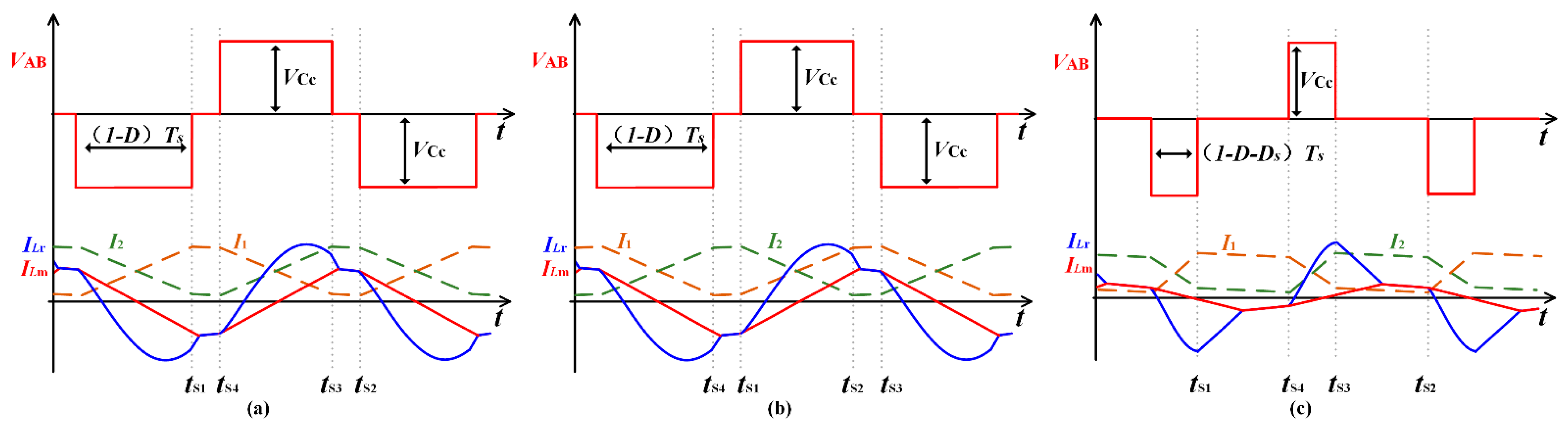
2.1. HG Mode
Fixed-frequency pulse-width-modulation control method with frequency fs is applied in the HG mode, and the switching frequency is equal to the LLC resonant frequency fr at rated condition.
The switches on the same bridge arm operate complementarily.
S1 and
S3 have the same duty cycle
D but have 180° phase-shift angles (
β = 180°), and the same is for
S2 and
S4. The input voltage of resonant tank
VAB is AC voltage with nearly rectangular waveform; the duty cycle equals to the minimum of
D and 1-
D, the maximum voltage equals to the
Vi/
D, and the sum voltage across the
Ns1 and
Ns2 equals to 0. The average value of
I1,
I2 are the same and equal to
Ii/2 due to the same value of coupled inductor
L1,
L2. The current ripple of
I1 and
Ii are denoted as Δ
ILs and Δ
Ii, respectively. Then, we obtain the following parameter definitions:
A switching cycle can be divided into 10 operational stages, and only the first five stages are analyzed in detail because the last five stages are symmetrical operations. The operating principles can be analyzed according to the key operational waveforms shown in
Figure 2 and
Figure 3, and they illustrate the corresponding equivalent circuits at the first five stages for
D > 0.5.
Stage 1 [
t0,
t1]:
S3 has been conducted before this stage and
S1 turns on under ZVS at
t0. The magnetizing voltage
VLm is clamped by the negative output voltage and
ILm decreases. The input voltage of resonant tank
VAB is equal to zero, and the resonant current
ILr increases in a sinusoidal manner at the resonant frequency
fr. In addition, the voltage across the
Ls1,
Ls2 is equal to
Vi–
VCc–
VL, and both of them are being discharged.
S1 and
S3 have been turned on, so
S2 and
S4 are clamped by the
VCc. The currents
ILr,
ILm and the voltage
VCr can be described as
Stage 2 [
t1,
t2]: At
t1,
ILr equals to
ILm. There are no current flows through the transformer’s winding during this stage, and there is no power transfer to the secondary side. Resonance begins between
Lr,
Lm, and
Cr at resonant frequency
fm.
ILr barely changes during this stage due to
Lm being greater than four times that of
Lr. Since
S1 and
S3 keep conducting in this stage, boost inductors
Ls1,
Ls2 are still being discharged, and
S2 and
S4 are still being clamped by the capacitor voltage
VCc. The currents
ILr,
ILm and the voltage
VCr can be obtained by
Stage 3 [t2, t3]: At the moment of t2, the drive signal of S3 drops to zero, S3 is turned off, and S1 still conducts. The converter enters the dead-time between S3 and S4. There is still no energy transfer to the secondary side, and the secondary diodes are in the off state. The junction capacitors of S3 and S4 begin to be charged and discharged, respectively.
Stage 4 [
t3,
t4]: At
t3, the voltage across the junction capacitor of
S4 declines to zero, and
S4 realizes the ZVS turn-on. During this stage, the input voltage of resonant tank
VAB is equal to the
VCc, and
VLm is clamped by the output voltage. Resonance happens between
Lr and
Cr, and primary resonant current
ILr increases in a sinusoidal manner at the resonant frequency
fr. The voltage across the
Ls1 and
Ls2 are
VCc–
Vi +
VH,
Vi–
VH, respectively. Moreover,
Ls1,
Ls2 are being discharged and charged, respectively, because
S1 and
S4 are turned on. And
S2,
S3 are being clamped by the capacitor voltage
VCc. Currents
ILr,
ILm, and the voltage across the resonant capacitor
VCr can be expressed as
Stage 5 [t4, t5]: At the moment of t4, S4 is turned off while S1 keeps on conducting. The converter enters the dead-time between S3 and S4 again. During this stage, the junction capacitors of S3 and S4 begin to be discharged and charged, respectively, by virtue of ILr and I2. The body diode of S3 starts conducting at the moment the voltage across junction capacitors of S3 decreases to zero. Thus, the ZVS turn-on of S3 can be realized.
The operation principles for the case D ≤ 0.5 are symmetrical to the analysis above.
2.2. MG Mode
The MG mode expands the zone of dead time
Ds between the switches on the same arm to obtain a lower voltage gain with
D > 0.5, and
Ds is defined as the phase shift angle from the falling edge of the gating signal of S
2 to the rising edge of that of S
1.
S1 and
S3 have the same duty cycle but have 180° phase-shift angles (
β = 180°), and the same is for
S2 and
S4. the key operational waveforms are shown in
Figure 4.
Stage 1 [
t0,
t1]: Before this stage,
S3 has been conducted,
S2 is turned off, the voltage across the
Ls1,
Ls2 is equal to
VCc–
Vi–
VL, and both of them are being discharged. After
t0,
S1 is turned on, this stage is similar to
Stage 2 of the HG mode,
ILr is equal to
ILm at
t0, and resonance begins between
Lr,
Lm, and
Cr at resonant frequency
fm. There are no current flows through the transformer’s winding during this stage and no power transfer to the secondary side. The currents
ILr,
ILm and the voltage
VCr can be obtained by
Stage 2 [t1, t2]: This interval is dead time between S3 and S4, which has not been expanded compared to HG mode.
Stage 3 [
t2,
t3]: At
t2,
S4 realizes the ZVS turn-on. This stage corresponds to
Stage 4 of the HG mode. The voltage across the
Ls1 and
Ls2 are
VCc–
Vi +
V1,
Vi–
V1, respectively.
Ls1,
Ls2 are being discharged and charged, respectively, because
S1 and
S4 are turned on. Currents
ILr,
ILm, and the voltage across the resonant capacitor
VCr can be expressed as
Stage 4 [
t3,
t4]: At the moment of
t3,
S4 is turned off and only
S1 still conducts. This stage is the main difference between HG mode and MG mode. During this stage,
VAB comes back to zero, the voltage across the
Ls1,
Ls2 is equal to
VCc–
Vi–
VL, and both of them are being discharged.
ILr decreases linearly and rapidly. Currents
ILr,
ILm, and the voltage across the resonant capacitor
VCr can be expressed as
After t4, the circuit enters the next half working state, and the working principle is similar to the first half cycle.
2.3. LG Mode
S1 and S3 are turned on and off at the same time in the LG mode (β = 0°), and so are S2 and S4, Ds = 0. The input voltage of resonant tank VAB is zero, and the output voltage is regulated by the variable duty cycle D. The operation principles of this circuit are somewhat similar to that of a forward converter.
A switching cycle can be divided into six operational stages, and the operating principles can be analyzed according to key operational waveforms in LG mode that are shown in
Figure 5 and
Figure 6. They illustrate the corresponding equivalent circuits at each stage in a switching cycle.
Stage 1 [t0, t1]: S1, S3 have been conducted before this stage. During this deadtime interval, the junction capacitors of S1 and S3 begin to charge and the junction capacitors of S2 and S4 begin to discharge. The voltage across the Ls1 and Lm1 are VL2, Vi–VCc–VL2, respectively. The magnetic reset circuit (composed of diode D1, winding Np11, Np21) is in an on state and stores the energy back into the power supply (charging the input capacitor C1), which also prevents the winding Np1, Np2 from generating too high reverse peak voltage and breaking down the switches. The voltage sum of winding NS1 and NS2 is negative, D3 conducts, and D2 is in off-state. The voltage across Lf is –Vo.
Stage 2 [t1, t2]: At t1, S2, S4 turn on. During this stage, diodes D2, D3 still conduct, the voltage of winding NS1, NS2 are clamped to zero, and the current flow through them is increasing. At the same time, the voltage across the Lf, Lm1, and Ls1 are –Vo, 0, and Vi, respectively. The current flow through D2 and Lf is ID2, ILf, respectively.
Stage 3 [t2, t3]: At the beginning of this stage, ID2 equals to ILf; that is, diode D3 is turned off. The power transferred to the load side is provided by the coupled-inductor L1 and L2. The voltage across the Lf, Ls1 are 2nIC(Vi–VH2)–Vo and VH2, respectively.
Stage 4 [t3, t4]: This time is deadtime interval, the junction capacitors of S1 and S3 begin to discharge and the junction capacitors of S2 and S4 begin to charge.
Stage 5 [t4, t5]: At the beginning of this stage, S1, S3 turn on. During this stage, diode D3 still conducts, the voltage of winding NS1, NS2 are clamped to 0, and the current flow through them is decreasing. At the same time, the voltage across the Lf, Lm1, and Ls1 are –Vo, 0, and Vi–VCc, respectively.
Stage 6 [t5, t6]: At the moment of t2, the current flow through the D2 equals zero; that is, diode D2 is turned off. The voltage across the Lf, Lm1, and Ls1 are –Vo, Vi–VCc–VL2, and VL2, respectively. The diode D1 conducts, and the magnetic reset circuit works again.
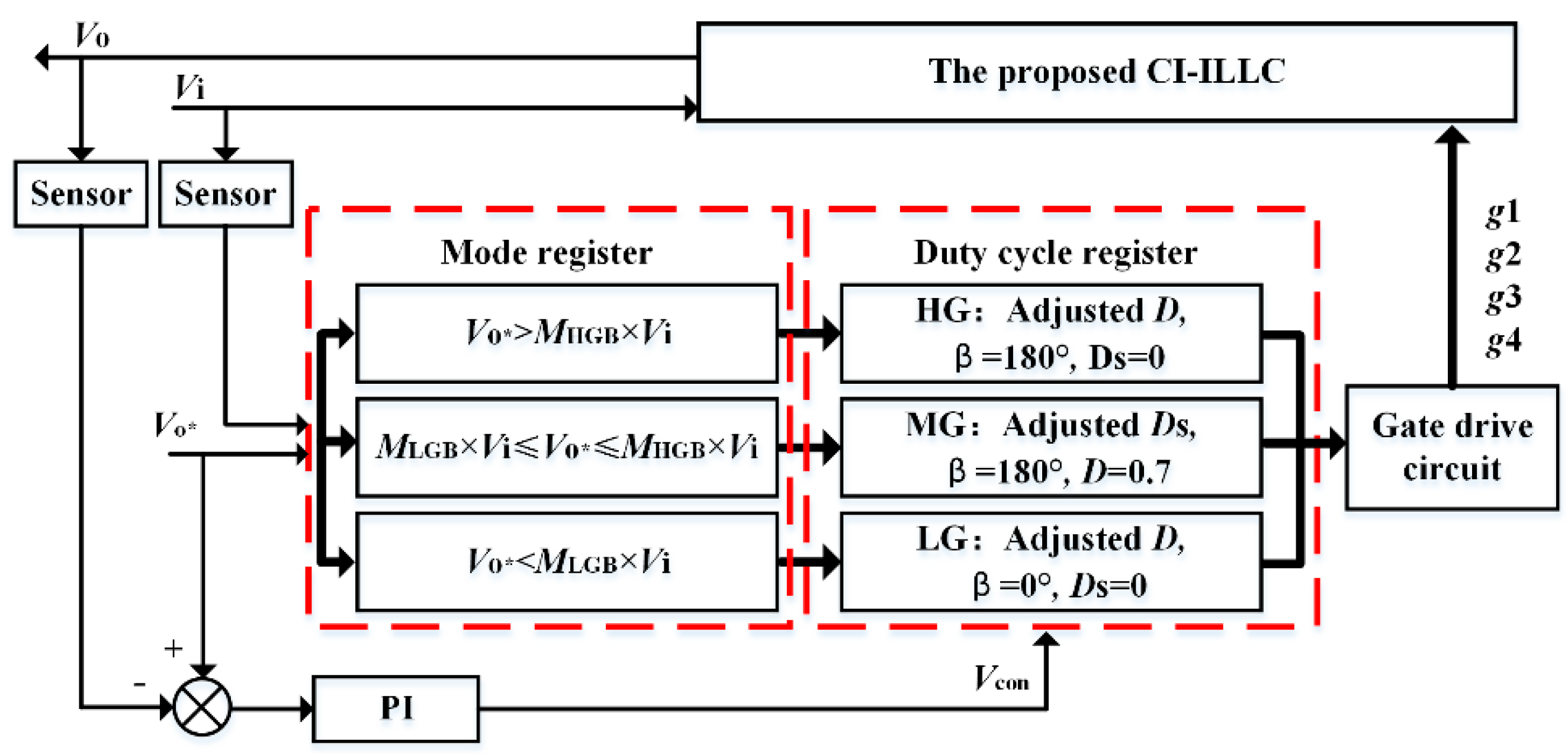
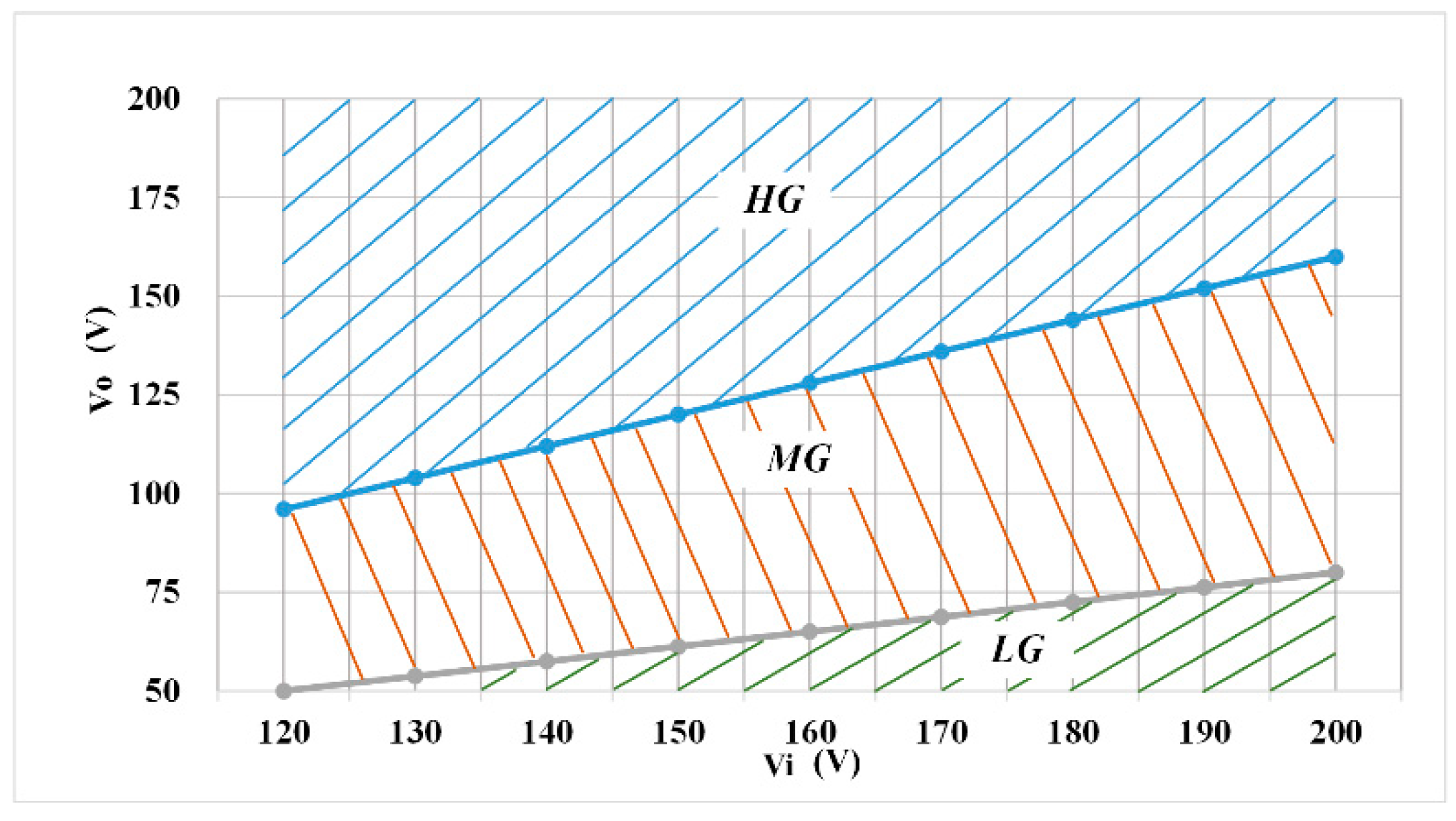
4. Control Methods of the Proposed CI-ILLC
The proposed CI-ILLC adopts fixed-frequency PWM to achieve output voltage regulation. Referring to
Figure 12, three modes are divided as follows:
- (1)
The boundary operation points of HG mode satisfy D = 0.7, Ds = 0.
- (2)
The boundary operation points of LG mode satisfy D = 0.57.
Figure 12.
Working range of three modes.
Figure 12.
Working range of three modes.
From the analysis in
Section 3.1, the boundary voltage gain of HG mode
MHGB with
D = 0.7, Q = 0.4 can be calculated as about 0.814, and the boundary voltage gain of LG mode
MLGB is obtained by substituting
D = 0.57 and load condition into (28)–(30).
The control block diagram is given in
Figure 13, and it uses a single-loop voltage controller. The controller is TMS320F28062; the input voltage
Vi and output voltage reference
Vo* are sent to the mode register to determine the gain mode. The output voltage
Vo is sampled and compared with voltage reference
Vo*, and their difference is transferred to a proportional-integral (PI) controller. Then, the output signal
Vcon is sent to the duty cycle register to adjust
D or
Ds. The duty cycle register corresponds to the modulation mode of different gain modes. When the
Vi and
Vo* change, the circuit will smoothly switch between HG, MG, and LG modes.
5. Topologies Comparison
A comparison with the current existing references and the proposed CI-ILLC is presented in
Table 1. The main superiorities of the CI-ILLC are as follows:
- (3)
Low current ripple:
High current ripple is one of the main disadvantages of the voltage-fed converter, which will hinder the improvement of efficiency. The interleaved structure is adopted in the proposed CI-ILLC, which does not only reduce the current ripple dramatically as proven in Ⅲ.B but also divides the input current into two transmission paths to reduce the current stress of switches.
- (4)
Wide operation range:
The proposed CI-ILLC can work with a wide operation range. The wide voltage gain range is achieved by the variable duty cycle. Besides, the proposed converter can work as a forward circuit at low power (low voltage) output conditions without the complex energy-flowing stage.
- (5)
High efficiency and power density:
A wide ZVS range can be achieved without the current reflow because CI-ILLC inherits the beneficial features of the LLC converter. Moreover, CI-ILLC obtains high power density based on multiplexing of coupled-inductors and switches with a simple structure.
In summary, the proposed CI-ILLC can be seen as a promising solution with a wide input voltage, wide output voltage, and high efficiency.
6. Simulation and Experiment Results
After simulating the proposed converter in SIMULINK, an experimental prototype has been built and tested with parameters listed in
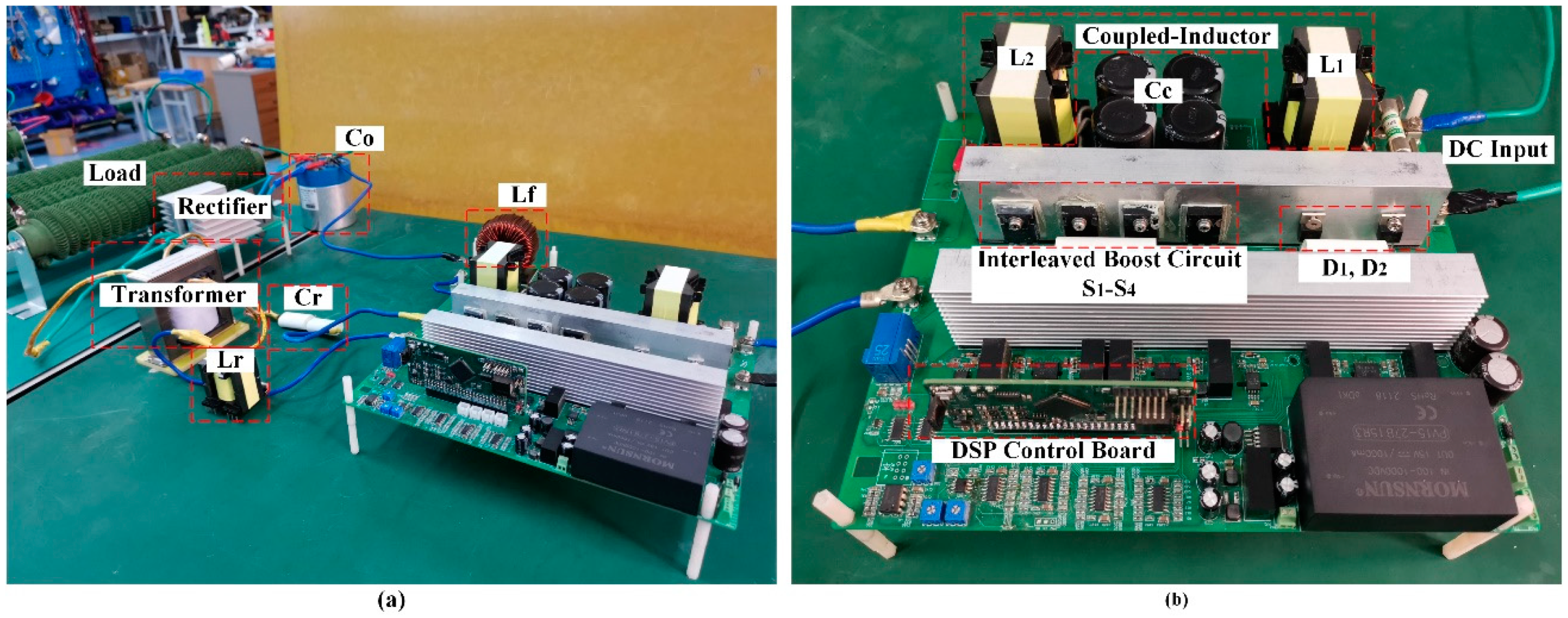
Table 2. The experimental prototype pictures are presented in
Figure 14. The design steps of the converter’s circuit components are given in the following:
- (1)
The equivalent frequency operates around resonant frequency; the voltage gain MDC is equal to 1/nD in HG mode according to (14). Under the consideration of the input and output voltage, n is chosen to be 1.6.
- (2)
The equivalent output resistance can be obtained by (15). The rated resonant frequency is set as 80 kHz, m and Q are chosen to be 10 and 0.4, respectively. Hence, the resonant capacitor Cr is calculated accordingly from (48)
- (3)
Cr is selected to be 110 nF, and resonant inductor Lr is obtained in the following equation:
Due to the limitation of the transformer, Lr is selected to be 38 µH, and Lm is equal to about 400 µH with m = 10.
- (4)
The magnetic reset circuit is composed of diode D1, winding Np11, Np21. In order to facilitate magnetic reset, nIC2 = np11:np1= np21:np2 is chosen to be 1:1 according to (31)–(34).
- (5)
The voltage gain of LG mode can be obtained from (28)–(30), and the minimum value of
D can be calculated from (34). In order to regulate the output voltage in LG mode zone as shown in
Figure 12,
nIC =
ns1:
np1=
ns2:
np2 is chosen to be 0.8:1.
Figure 14.
(a) Experimental platform; (b) prototype hardware.
Figure 14.
(a) Experimental platform; (b) prototype hardware.
Table 2.
Parameters of Experimental Prototype.
Table 2.
Parameters of Experimental Prototype.
| Parameters | Values | Parameters | Values |
|---|
| Input voltage (Vi) | 120–200 V | Rated power (Po*) | 75–1200 W |
| Output voltage (Vo) | 50–200 V | Rated switching frequency (fsn) | 80 kHz |
| Turns ratio of transformer (n) | 1.6:1 | Turns ratio of coupled inductor (nIC) | 0.8:1 |
| Turns ratio of coupled inductor (nIC2) | 1:1 | Leakage inductors of coupled inductor (Ls1, Ls2) | 130 μH |
| Magnetic inductor of transformer (Lm) | 400 μH | Magnetic inductors of coupled inductor (Lm1, Lm2) | 1 mH |
| Resonant capacitor (Cr) | 110 nF | Resonant inductor (Lr) | 38 μH |
| Output inductor (Lf) | 1 mH | Clamp capacitor (Cc) | 220 μF |
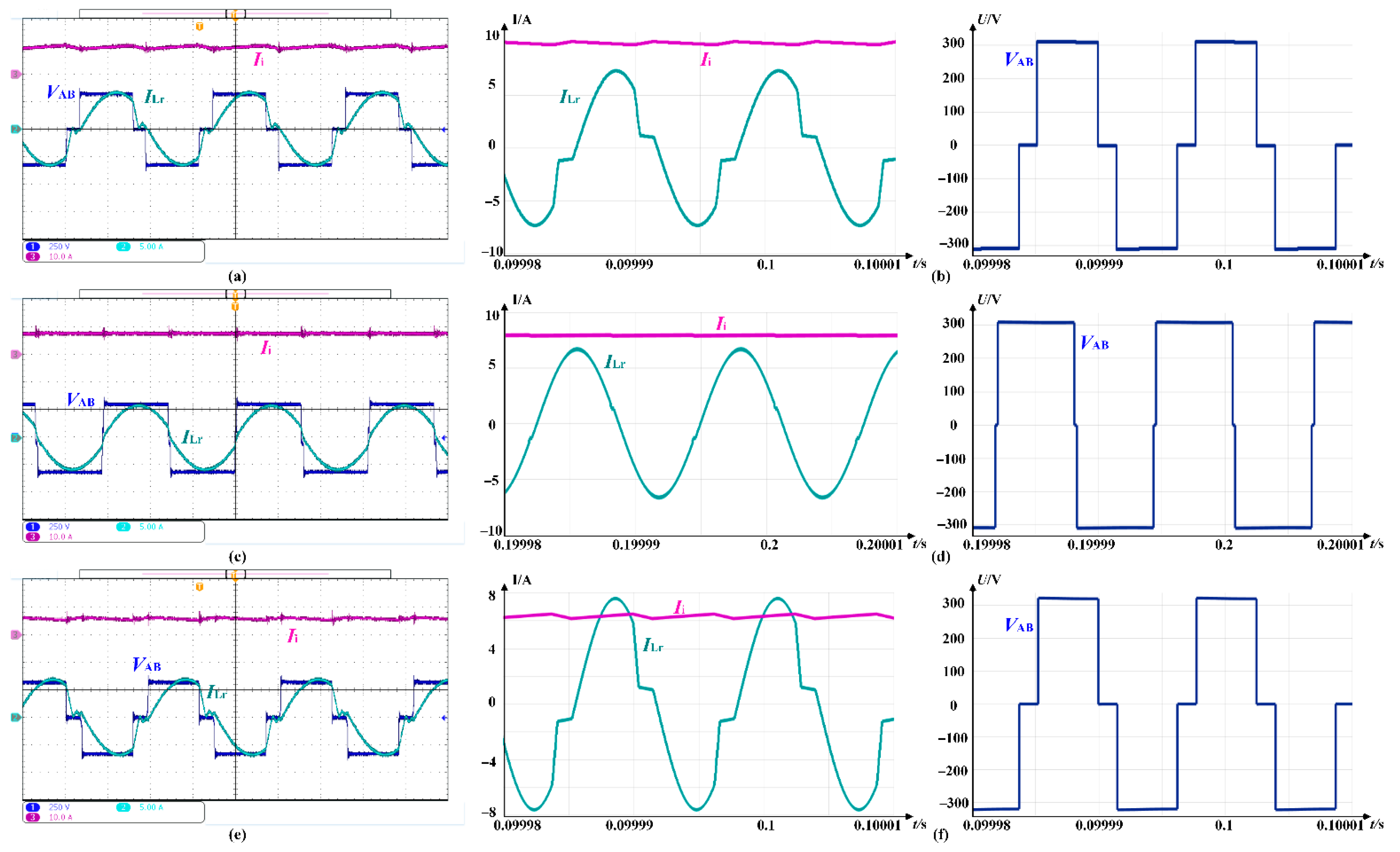
Figure 15 demonstrates the simulation waveform of
VLs1,
VLs2,
I1,
I2 in HG mode under rated power conditions with different input voltages.
I1 and
I2 are operated at a phase difference of 180° with the same amplitude, and so are
VLs1 and
VLs2. The current ripples of
I1,
I2 are about 6–8 A over a wide input voltage range of 120–200 V. The simulated and experimental waveforms of HG mode under rated power conditions with different input voltages are presented in
Figure 16. The output voltage of the proposed CI-ILLC is regulated by fixed-frequency PWM control. The duty cycle of the input voltage of resonant tank
VAB in HG mode is equal to the minimum value between the
D and 1–
D. The duty cycle range of CI-ILLC at full-loaded is 0.37–0.62 over the input voltage range of 120–200 V. Though the current ripple of
I1 and
I2 is relatively large, the current ripple of
Ii is reduced dramatically, especially duty cycle close to 0.5, which verifies the current ripple suppression mechanism of the proposed CI-ILLC.
The simulated and experimental waveforms of MG mode under different operation points are presented in
Figure 17. The resonant stage of the MG mode corresponds to the HG mode. With the increases of
Ds, the duty cycle and magnitude of the input voltage of resonant tank
VAB decreases, which is equal to 1–
D–
Ds and (1–
Ds)
Vi/
D, respectively. The experimental results manifest that the proposed converter possesses excellent voltage regulation capability by adjusting
Ds in the range of 0–0.15 at MG mode.
The simulated and experimental waveforms of LG mode under different operation points are illustrated in
Figure 18. The voltage across couple-inductor
L1 increases as the input voltage increases. There are significant differences between the waveforms of the experiment and simulation due to the existence of interlayer capacitors in the coupled inductor. The interaction of interlayer capacitors and leakage inductors causes the voltage oscillation of magnetic inductor
Lm1 and
Lm2. Then, this oscillation is also reflected in
ILf,
VLf,
I1,
I2. However, this oscillation affects the voltage gain slightly, and the variation trend and the average value of them are the same in experiment and simulation, which is verified in
Figure 18 and consistent with the analysis in
Section 2.
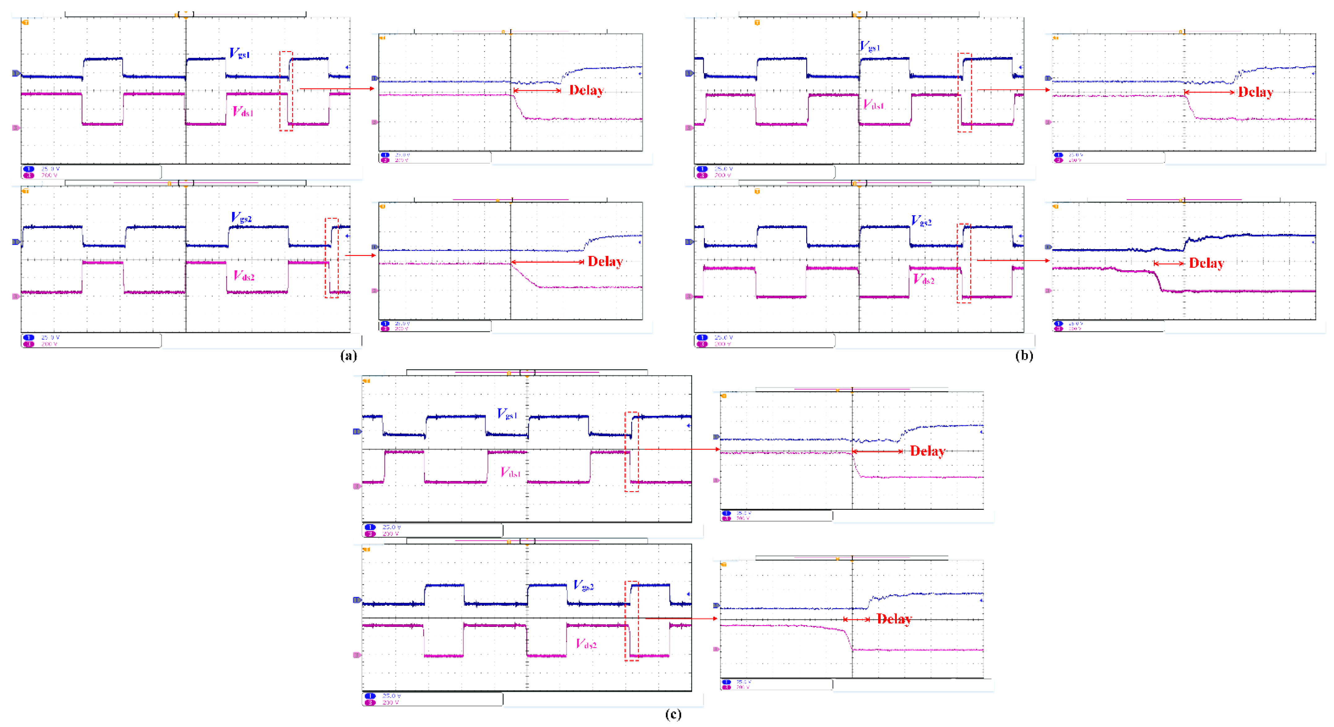
As analyzed above, the ZVS condition of
S3 and
S4 are the same as that of the
S1 and
S2 due to the symmetry of topology and modulation. The experimental results of
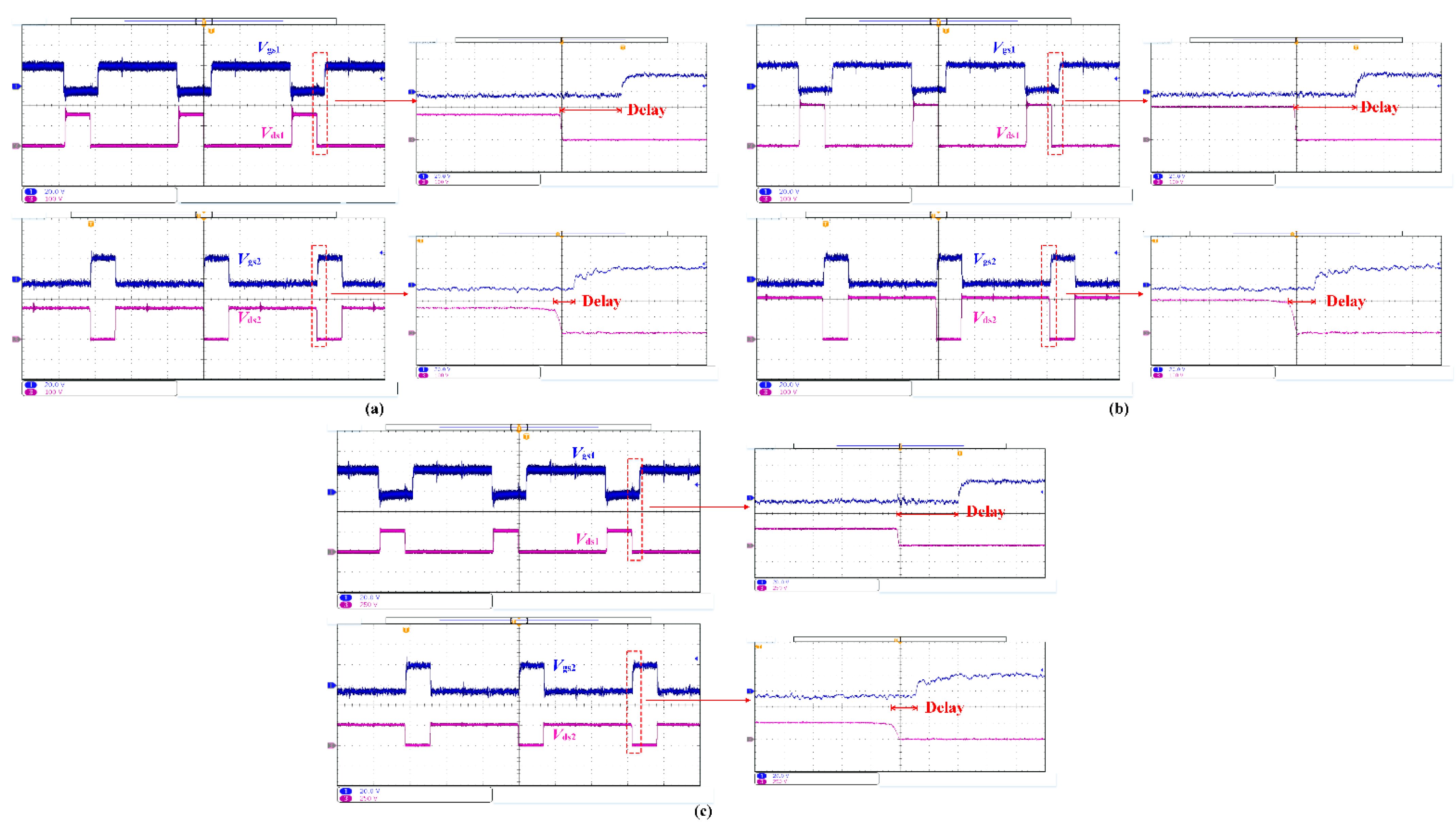
S1 and
S2 with different input voltage under full load are provided in
Figure 19, meanwhile, their enlarged view is also provided to exhibit the time delay. It is obvious that the drain-source voltages of
S1 and
S2 decrease to zero before the driving signal
Vgs1 and
Vgs2 start rising, which means that the ZVS condition of
S1 and
S2 is achieved. As can be seen, the delay between the
Vds1 decreases to zero, and
Vgs1 start rising is always greater than 120 ns, which means that
S1 can realize ZVS easily over a wide range and agree with the theoretical analysis above. Therefore, the snubber circuit for active switches is not necessary for the proposed CI-ILLC. However, the delay between
Vds2 and
Vgs2 is decreasing from 160 ns to 60 ns with the input voltage and load increasing. Moreover, the voltage across switches is also presented in
Figure 19, and the voltage stress always equals the
Vcc =
Vi/
D in HG mode, regardless of output load.
The experimental results of
S1 and
S2 in MG mode under different operation points are illustrated in
Figure 20. As can be seen, the delay between the
Vds1 decreases to zero and the
Vgs1 start rising is always greater than 800 ns due to the existence of
Ds, which provides enough time to discharge the junction capacitor. However, the delay between
Vds2 and
Vgs2 is less than 60 ns with the input voltage and load increasing, and the ZVS condition becomes harder.
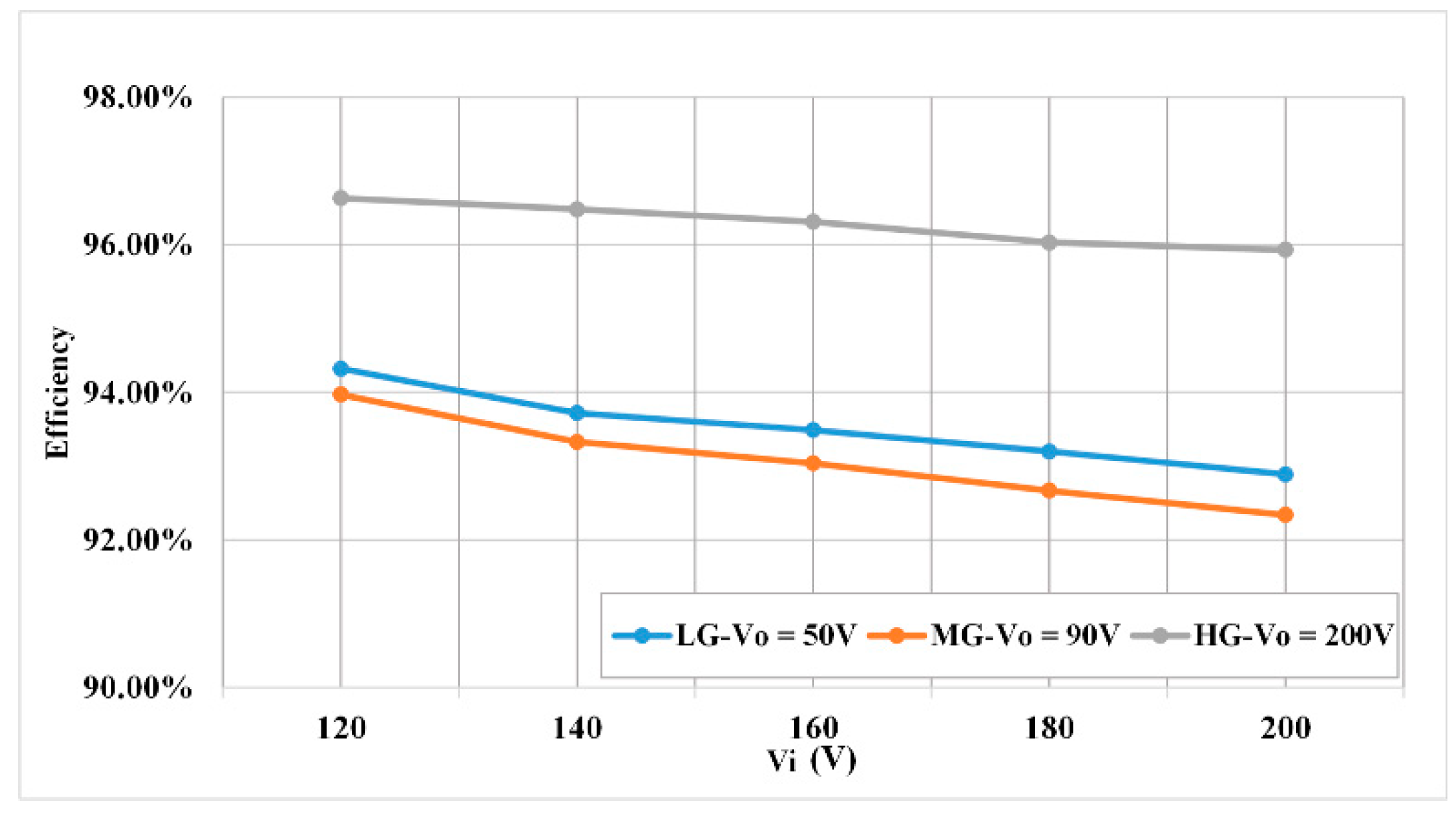
Figure 21 shows the measured efficiencies of the proposed CI-ILLC with the different input voltage in both HG, MG, and LG modes It can be found that the proposed converter has high efficiency more than 92% over the whole operation range. At rated load, the peak efficiency can reach 96.6% in HG mode.


