Article

Seven-Level Inverter with Reduced Switches for PV System Supporting Home-Grid and EV Charger

by
Ahmed Ismail M. Ali
1,*,
Mahmoud A. Sayed
1 and
Ahmed A. S. Mohamed
2
1
Department of Electrical Power and Machines Engineering, Faculty of Engineering, South Valley University, Qena 83523, Egypt
2
Center for Integrated Mobility Sciences, National Renewable Energy Laboratory (NREL), Golden, CO 80401, USA
*
Author to whom correspondence should be addressed.
Energies 2021, 14(9), 2718; https://doi.org/10.3390/en14092718
Submission received: 8 April 2021 / Revised: 4 May 2021 / Accepted: 5 May 2021 / Published: 10 May 2021
(This article belongs to the Special Issue Electric Vehicles in a Smart Grid Environment)

Abstract

:
This paper proposes a simple single-phase new pulse-width modulated seven-level inverter architecture for photovoltaic (PV) systems supporting home-grid with electric vehicle (EV) charging port. The proposed inverter includes a reduced number of power components and passive elements size, while showing less output-voltage total harmonic distortion (THD), and unity power factor operation. In addition, the proposed inverter requires simple control and switching strategies compared to recently published topologies. A comparative study was performed to compare the proposed inverter structure with the recent inverter topologies based on the number of components in the inverter circuit, number of components per output-voltage level, average number of active switches, THD, and operating efficiency as effective parameters for inverter performance evaluation. For design and validation purposes, numerical and analytical models for a grid-tied solar PV system driven by the proposed seven-level inverter were developed in MATLAB/Simulink environment. The inverter performance was evaluated considering grid-integration and stand-alone home with level-2 AC EV charger (3–6 kW). Compared with recently published topologies, the proposed inverter utilizes a reduced number of power components (7 switches) for seven-level terminal voltage synthesis. An experimental prototype for proposed inverter with the associated controller was built and tested for a stand-alone and grid-integrated system. Due to the lower number of ON-switches, the inverter operating efficiency was enhanced to 92.86% with load current THD of 3.43% that follows the IEEE standards for DER applications.

1. Introduction

Recently, the world witnessed several storms and crises that disturbed most of the energy sources around the world, which forced them to switch to standstill energy sources allowing only emergency supplies. Therefore, many industries were been brought to a standstill during supply interruption and fuel lack. For such scenarios, renewable energy, especially the solar photovoltaic (PV) energy, stand out for making up the energy balance. Additionally, negative environmental impacts, along with the unsustainable nature associated with conventional energy resources, i.e., fossil fuels, provoke the development of new and clean energy resources to satisfy the increased global energy demand [1,2]. Among the different renewable energy resources, solar PV and wind energy are the most popular resources [3,4,5] which have been exploited by different companies and countries. Moreover, the renewable energy trend relies on electrical energy production from commercial and residential buildings using PV systems that help to enhance the power system resilience. Given the flexibility associated with PV systems, they are an ideal source of electricity for remote areas, which are located far away from local utility-grids [2,6]. Hence, energy can be produced by installing PV panels on household rooftops for direct consumption, where the excess energy can be stored or sold to the grid if the system is grid-connected. In addition, PV systems can be used to support new emerging loads, e.g., electric vehicle (EV) charging [7]. Considering energy generation, storage, and self-consumption, EVs production arises as a crucial part of smart offices and residential buildings [8,9]. In addition to reducing CO2 emissions and costs, EVs have the potential to significantly enhance self-supplying and consumption [10,11].
A critical component to integrate renewable energy sources with other systems is the power electronics interface converter, which is witnessing rapid development in conjunction with the widespread use of these new technologies. Due to the intermittent DC-power of the PV systems, power converters are vital to regulate the system output and facilitate their integration with the grid and other loads, e.g., AC charging ports for EV [12,13]. The multilevel inverters (MLIs) evaluation has been initiated in [14], based-on the neutral-point clamped structure (NPC) for medium/high power applications. MLI architectures offer many features compared to conventional topologies such as low voltage-stress on the switches, low voltage-ratings, reduced THD, reduced electromagnetic interference (EMI), voltage boosting capability in single-stage operation, and enhanced power-quality of the grid-integrated system with reduced filter passive elements [13,15]. The conventional topologies of MLIs are divided into three categories: cascaded H-bridge (CHB-MLI) [16,17], NPC-MLI [18,19], and flying capacitor (FC-MLI) [20,21]. Despite the large number of output-voltage levels that are synthesized from these topologies, many power switches are needed, which surges the converter’s power loss and complicates the control circuit design and implementation in addition to negatively impacting the inverter reliability.
To mitigate the former drawbacks, modified MLI architectures are introduced based-on a reduced number of components [22,23,24,25,26,27,28,29,30,31,32]. In [22], a seven-level pulse-width-modulation (PWM) inverter is presented considering external DC input sources and suitable circuit combination for switches and THD reduction. However, it required a comparatively increased number of switches and external DC-sources, which increased the inverter footprint and cost. In [23], a staircase MLI is presented to decrease the number of power components and the inverter losses. However, this topology considers an even larger number of switches. In [24], the number of external DC-sources is reduced without voltage division over input split-capacitors. However, this topology can be used for up to five-level synthesis without modular extension capability. For further reduction of switches, MLI with reduced switches is presented in [25], but it requires a large number of separated DC-sources for output voltage synthesis. In [26], a new inverter structure basic cell is presented considering a reduced number of switches to a competitive level. However, this architecture still requires a large number of separate DC-sources, and it is only applicable for high output-voltage levels that complicate the control scheme and switching pattern. In [27], a new single-phase MLI inverter was introduced with a voltage-boosting capability for low voltage PV systems. However, it is applicable for low power applications and it incorporates two conversion stages, which increases the power losses. In [28], a compact MLI is presented considering a reduced number of external DC-sources using two-capacitors in each module for staircase multilevel output-voltage. However, this increases the inverter power density and footprint for high power applications. New MLI topologies for single/three-phase applications considering a reduced number of components and a single DC-source are recommended for renewable energy applications [29,30]. Different MLI topologies are developed to reduce the inverter power loss, voltage-stress, and overall footprint using different switching and commutation techniques [33,34]. In addition, several MLI structures are proposed to improve the stand-alone and grid-integrated renewable energy and EV applications at improved operating efficiency.
Motivated by the literature survey, this paper proposes a new single-phase 7-level PWM inverter, considering a reduced power component count, for stand-alone and grid-integrated PV systems. The proposed inverter reduces the required number of components to a competitive level for efficiency, footprint, and cost improvements. The proposed MLI is divided into two circuits: the main and auxiliary. The main circuit is a simple H-bridge inverter circuit, which is responsible for output-voltage polarity control, and the auxiliary circuit is a combination of switches to synthesize each output-voltage level. In addition, a boost converter (BC) is internally integrated with the PV-array for maximum power point tracking (MPPT) at the front-end of the 7-level inverter, as indicated in Figure 1. A simple sinusoidal level shifted PWM switching technique is used for gating the power switches of the proposed inverter for a less complex control technique. The output-voltage levels that can be synthesized are: +Vdc, +2Vdc/3, +Vdc/3, 0, −Vdc/3, −2Vdc/3, and −Vdc.
The rest of the paper is organized as follows. Section 2.1 deliberately illustrates the proposed inverter circuit configuration, and the switching pattern, control algorithm, and switching logical combinations are demonstrated in Section 2.2. In addition, a comparative study of the proposed 7-level inverter with the recent inverter topologies is interpreted and discussed in Section 3 to show the features of the proposed inverter for industrial applications. The proposed system control scheme is discussed in Section 4. The proposed 7-level inverter simulation and experimental validations for grid-integrated PV system supporting L2 AC EV charging are analyzed in Section 5. Finally, Section 6 concludes the paper findings.
The circuit diagram of the proposed 7-level inverter is depicted in Figure 2. The inverter circuit is divided into two portions: the main and auxiliary circuit. The main involves an H-Bridge inverter that incorporates four power switches (S1, S2, S3, and S4) and is responsible for generating the positive and negative half cycles. On the other side, the auxiliary circuit of the 7-level inverter consists of three power switches (Qf, Q1, and Q2), two batteries (Vdc1 and Vdc2), and a single power diode (DA), as illustrated in Figure 2. The main purpose of the auxiliary circuit is to synthesize the different output-voltage levels and deliver these voltage levels to the front-end of the H-bridge inverter. Hence, the switching device of the auxiliary circuit is operating at the switching-frequency similar to the other stage.

2. Proposed Multilevel PWM Inverter

2.1. Circuit Configuration and Operation Principal

The front-end of the inverter auxiliary circuit is connected to the main DC source, which is the output DC voltage from BC in a PV system that will be clearly illustrated later in this paper. The MLI operation is simply demonstrated as appeared in Figure 3 and Figure 4. Switching-ON Qf results in having the total DC-voltage Vdc (Vdc = Vdc1 + Vdc2) applied to the front-end of H-bridge circuit and the two batteries charge in series at the same time through diode forward biasing (DA) where:
V d c 1 = 1 2 V d c 2 = 1 3 V d c
On the other side, switching-OFF the series switch (Qf) isolates the input DC-source from the H-bridge front-end allowing the charged series batteries to discharge during an adequate duration determined by the control strategy to supply the utility grid. The circuit operation can be divided into seven modes illustrated in Figure 3 and Figure 4 and described as follows:
  • Mode 1, the series switch (Qf) is ON to connect the DC-source Vdc to the front-end of H-bridge circuit. By switching-ON of the two switches S1 and S4, the inverter output voltage becomes +Vdc. At the same time, the two batteries (Vdc1 and Vdc2) charge through the diode (DA), as described in Figure 3a. Then, the reverse current path is illustrated in Figure 3b.
  • Mode 2, switching-OFF Qf isolates the DC supply. At the same time, the switch (Q2) is turned on to apply a voltage of 2Vdc/3 to the H-bridge circuit and the second battery is disconnected from the circuit and diode DA is reversed. Turning-ON switches S1 and S4 of the main inverter results in generating output-voltage of positive +2Vdc/3, as clarified in Figure 3c. The reverse current path is depicted in Figure 3d.
  • Mode 3, the series switch (Qf) as well as (Q2) are OFF-stated. Switch (Q1) is turned-ON to apply a DC-voltage of Vdc/3 to the H-bridge circuit. Similarly, turning-ON switches S1 and S4 of main circuit synthesizes output-voltage of +Vdc/3, as depicted in Figure 3e. The reverse current path is shown in Figure 3f.
  • Mode 4, the zero output-voltage can be generated by voltage cancellation through the main H-bridge inverter. Voltage cancellation occurs by switching-ON (S1 and S3) or (S2 and S4) as shown in Figure 3g,h.
  • Mode 5, the series switch (Qf) as well as (Q2) are OFF-stated same as to mode (3). The switch (Q1) is turned-ON to deliver DC voltage of Vdc/3 to H-Bridge input side. Turning-ON switches S2 and S3 of the main inverter generates an output-voltage of −Vdc/3, as shown in Figure 3i, where the reverse current path is depicted in Figure 3j.
  • Mode 6, turning-OFF the series switch (Qf) and switching-ON (Q2) delivers a voltage of 2Vdc/3 to the H-bridge inverter similar to Figure 3c. At the same time, switching-ON switches (S2 and S3) of the main inverter synthesizes a negative output-voltage of (−2Vdc/3), as clarified in Figure 3k. The reverse current path is portrayed in Figure 3l.
  • Mode 7, turning-ON the series switch (Qf) applies the total DC-voltage Vdc to front-end of H-Bridge inverter. By turning-ON the two switches S2 and S3, MLI output-voltage becomes −Vdc. At the same time, the two batteries (Vdc1 and Vdc2) are charging in series through diode (DA) similar to mode (1), as shown in Figure 3m. Besides, the current path of the reverse direction is shown in Figure 3n.
The logical combination of switching patterns of the auxiliary circuit and H-bridge inverter switches simplifies the switching pattern of the proposed inverter. Using a suitable control strategy, 7-levels output-voltage of +Vdc, +2Vdc/3, +Vdc/3, 0, −Vdc/3, −2Vdc/3, and −Vdc can be synthesized from the proposed inverter that enhances the power quality of the grid-integrated operation.

2.2. The Switching Patterns and Control Strategy

The pulse-width modulated switching scheme of the 7-level inverter is depicted in Figure 4. The switching pattern of the proposed inverter uses a rectified sinusoidal waveform reference signal and three high-frequency carrier-signals. The reference signal has the same power-frequency as the required output voltage. The carrier waveforms have the same frequency and amplitude with different offset (level-shifted PWM) to generate the appropriate switching pattern of the power switches. By comparing the reference signal with level-shifted carrier waveforms, the gating signals of each inverter switch can be generated, as shown in Figure 4; when VCar1, VCar2, and VCar3 are lower than VRef, the switching functions of all switches are OFF. During the positive half-cycle and when VRef is higher than VCar1 and lower than VCar2 as well as VCar3, it represents operational mode (3), as shown in Figure 3e. Similarly, during the negative half-cycle and when VRef is higher than VCar1 and lower than both VCar2 and VCar3, it describes operational mode (7), as indicated in Figure 3i. When VRef > VCar1 and VCar2 and lower than VCar3, it represents the operational mode (2), as depicted in Figure 3c. Along the same vein, when VRef > VCar1 and VCar2 and lower than VCar3, that describes mode (6), as shown in Figure 3k. Finally, when VRef is higher than VCar3, the switch Qf is turned-ON to deliver the total input DC-voltage to the H-bridge circuit to synthesize the third output-voltage level, as described in modes (1) depending on the H-bridge inverter switching, as portrayed in Figure 3a,b, respectively.
Considering one output-voltage/reference signal cycle, the switching functions are divided into six modes of operation related to the output-voltage levels, where the full switching states based on the comparison between the reference and carrier waveforms are listed in Table 1, and the corresponding operating periods are determined by:
Mode 1: P1 → 0 < ωt < θ1 and P5 = θ4 < ωt < π
Mode 2: P2θ1 < ωt < θ2 and P4 = θ3 < ωt < θ4
Mode 3: P3θ2 < ωt < θ3
Mode 4: P6π < ωt < θ5 and P10 = θ8 < ωt < 2π
Mode 5: P7θ5 < ωt < θ6 and P9 = θ7 < ωt < θ8
Mode 6: P8θ6 < ωt < θ7
By logical combinations of the different switching functions (Qf, Q1, …. etc.) and the operational modes (P1, P2, …, Pn), the switched gating pulses can be generated for each switch (Sn). Also, application of gate pulses to the switches during each fractional period depends on the switching angle (θn) and the modulation index/ratio (Ma);
M a = A m 3 A c
where; Am is the reference-signal amplitude, and Ac is the amplitude of carrier waveforms. The synthesized output-voltage can be formulated as follows:
v o u t = M a sin ( ω t )
Consequently, the switching functions of the auxiliary circuit switches can be simply generated based-on the aforementioned key switching waveforms using the appropriate combinations of logic-gates (AND, OR, and NOT) as follows:
Q 1 = ( S 1 + S 3 ) × Q * × S 1 ¯
Q 2 = S 1 × Q *
To illustrate the effect of different modulation ratios on the output-voltage levels, different modulation indices are considered under different output-voltage levels. When Ma is lower than 0.33, the output-voltage has only three levels (+Vdc/3, 0, −Vdc/3). For a modulation index between 0.33 and 0.67, the output-voltage shows five levels (+2Vdc/3, +Vdc/3, 0, −Vdc/3, −2Vdc/3). For a modulation index between 0.67 and 1, 7-level output-voltage can be synthesized (+Vdc, +2Vdc/3, +Vdc/3, 0, −Vdc/3, −2Vdc/3, −Vdc).

3. Comparative Study

This section introduces a comparative study between the proposed 7-level PWM inverter with the recent MLI structures based on different performance metrics, such as number of switching devices, number of components, number of components for each output-voltage level (NC/L), number of active switches per output-voltage pole (NAVG/Pole), output-voltage THD, inverter efficiency, and the applied PWM technique. The comparison illustrates that each MLI topology utilizes different number of components to obtain the same output-voltage level. As NC/L increases, the MLI topology requires more components for same output-voltage level synthesis per pole. On the other side, when NC/L has decreases, the required number of components decreases, which enhances the inverter efficiency. The factor (NC/L) can be formulated as follows [13]:
N C / L = N C + N T + N S + N D + N P S + N X N P o l e
where;
  • NC/L: Components per pole of output voltage level.
  • NPole: Number of voltage levels per pole.
  • NC: Number of capacitors.
  • ND: Number of diodes.
  • NS: Number of switching devices.
  • NPS: Number of DC power supplies.
  • NT: Number of transformers.
  • NX: Number of additional components.
Table 2 illustrates a comparison between the proposed inverter topology and the recent topologies based-on the former metrics. As noted, the proposed MLI utilizes a smaller number of power switches, power components, and NC/L compared to other topologies. This leads to fewer losses and less cost associated with the proposed inverter. In addition, NAVG/Pole is compared for the different MLI topologies as an indication for the number of active switches in the current path, which indicates the inverter power-losses. The factor NAVG/Pole can be expressed as follows:
N A V G / P o l e = N l e v e l ( 0 ) + N l e v e l ( 1 ) + N l e v e l ( 2 ) N P o l e
where;
  • Nlevel(0): number of active switches for the zero output-voltage synthesis.
  • Nlevel(1): number of active switches for the first output-voltage level synthesis.
  • Nlevel(2): number of active switches number for the second output-voltage level synthesis.
Based-on Table 2, the proposed MLI exhibits a low NAVG/Pole in compared with most of the recent added topologies, which decreases the inverter power losses and enhances its efficiency. In addition, the heat dissipated over the inverter components is reduced, which improves the system reliability. Figure 5 shows NS, NC/L, NAVG/Pole, and THD for the proposed 7-level inverter in compared with the recent MLI structures.

4. MLI Control Scheme

Control scheme of the proposed single-phase 7-level inverter with MPPT algorithm for stand-alone and grid-integrated operations is depicted in Figure 6. A single choke-coil was used as current filter for sinusoidal grid-integrated voltage and current. The conventional P&O algorithm was used for MPPT, in which the PV array voltage and current were sensed and used to define the BC duty cycle that matches MPP [2,46,47]. The MPPT controls the maximum power to the load/grid considering a constant (K) that defines the system tracking efficiency. Different linear and non-linear controllers can be used for load-voltage/grid-current regulation; however, the conventional PI-controller was used in this work due to their simplicity and linearity [48,49]. In both cases, the reference set point was usually used as a sinusoidal waveform [30,50]. In case of grid-integrated operation, the reference set point was used as the sinusoidal grid-voltage to ensure the unity power factor operation. Hence, the PV system power was divided by the grid voltage to produce the sinusoidal reference grid-current, as shown in Figure 6. In stand-alone operation, the reference set point was a sinusoidal waveform for the desired load voltage. A closed-loop current control using the conventional PI controller is used to regulate the actual grid-injected current (ig) to follow the reference value (ig*) considering the proposed PWM switching pattern. The PI controller output-signal was considered as the modulation index signal (Ma), which was compared with the level-shifted carrier waveforms to generate the key gating pulses (S1, S2, S3, and S4). Then, the auxiliary circuit switching pulses could be derived based-on Equations (10) and (11).

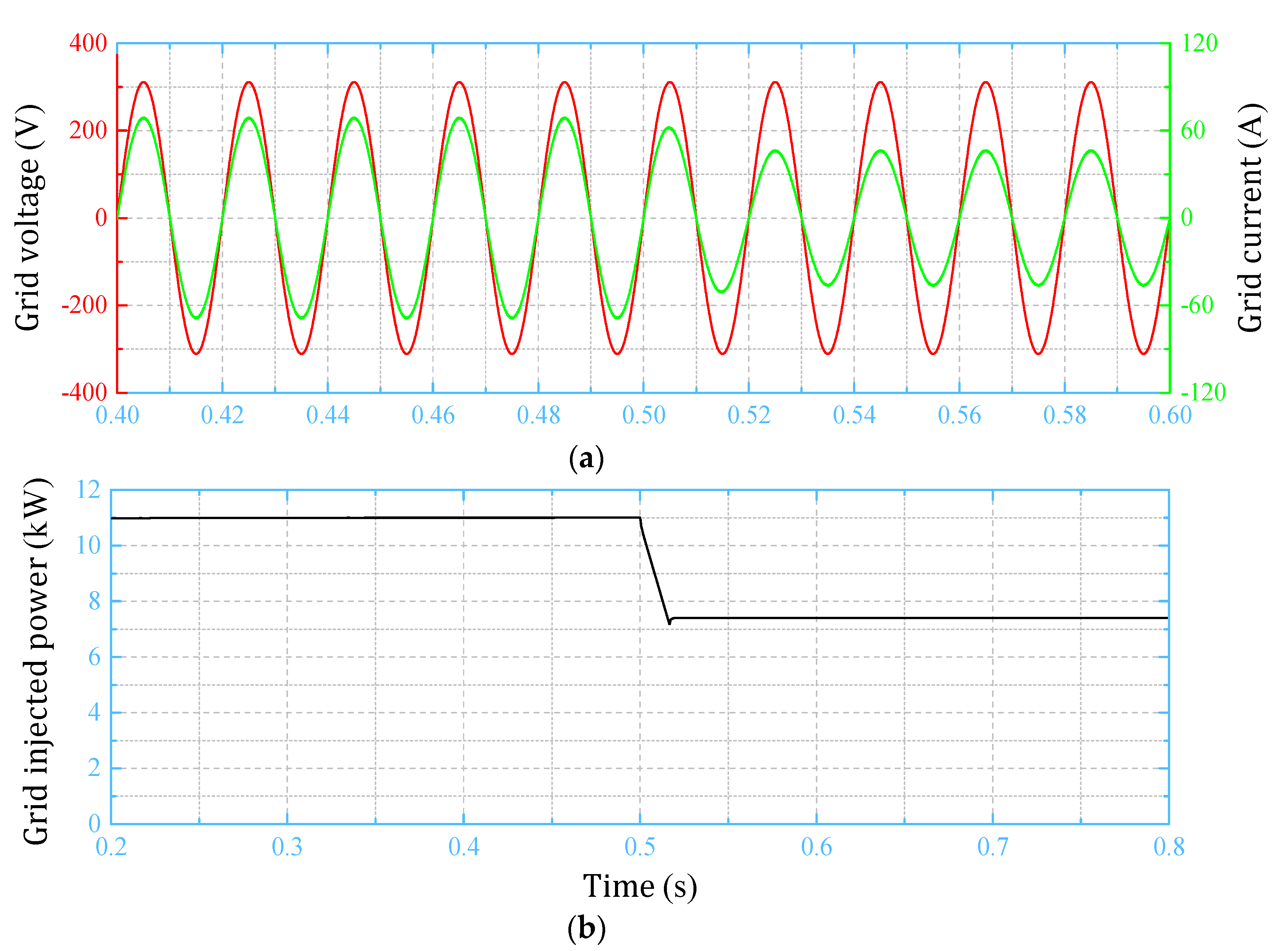
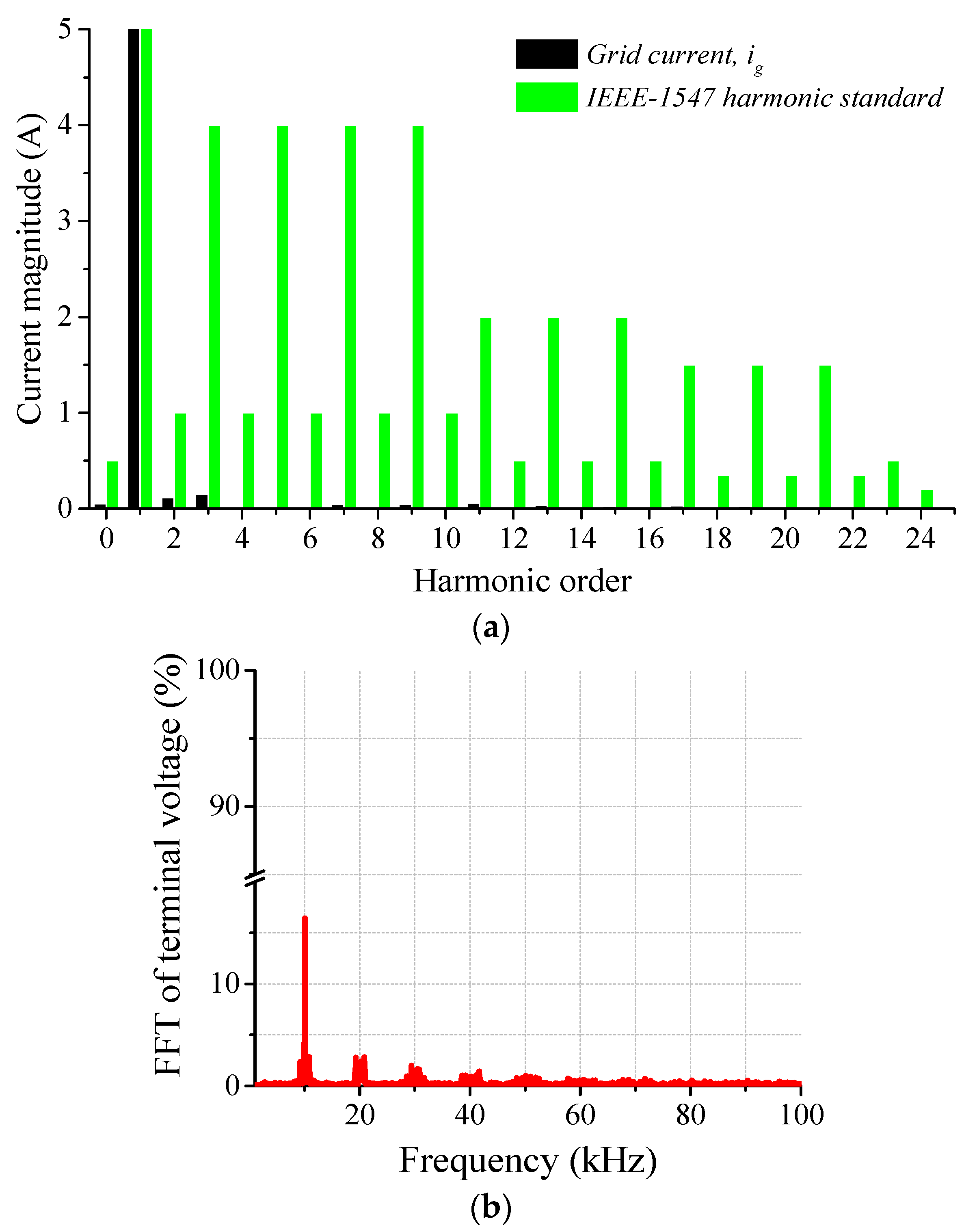
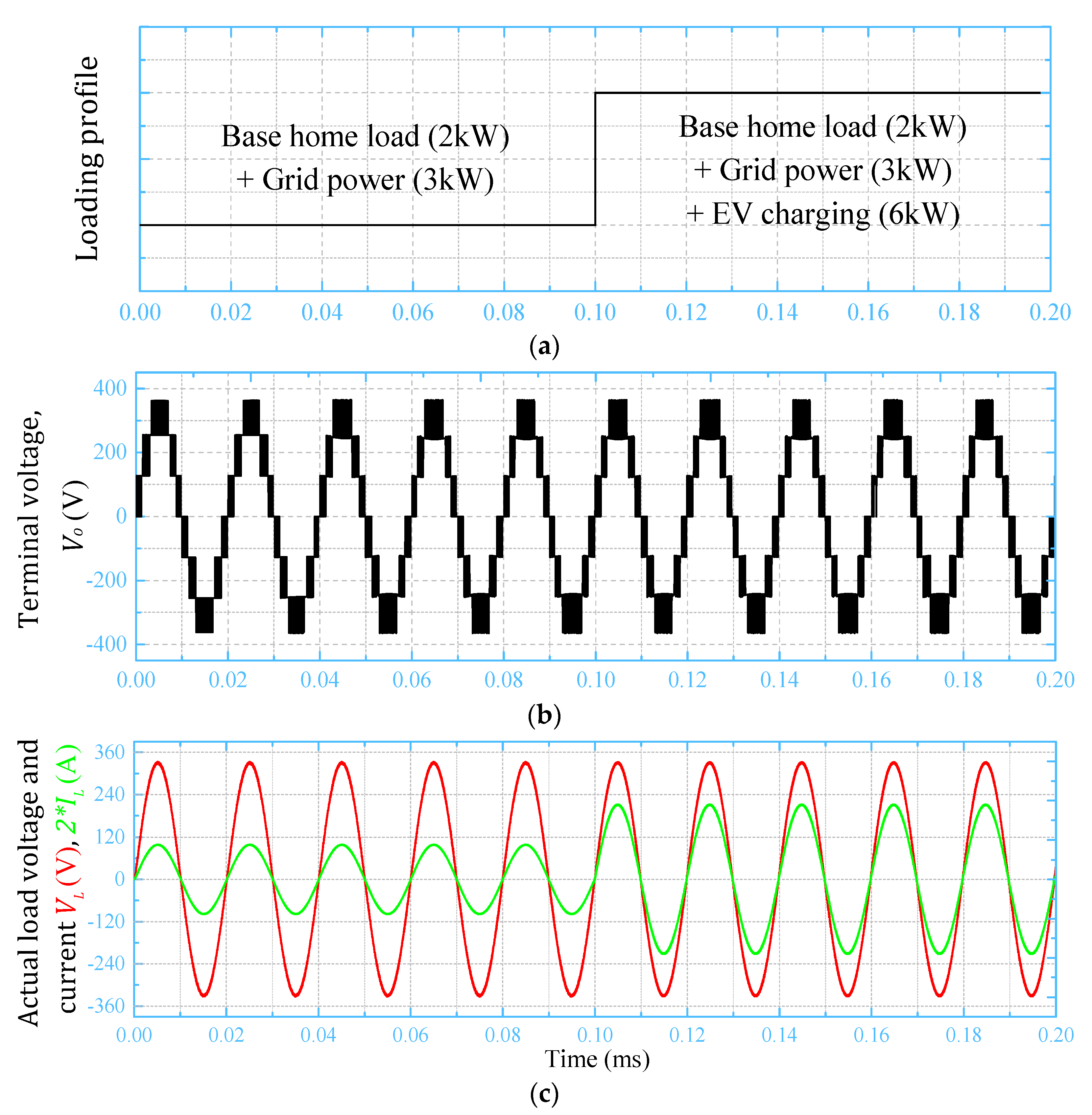
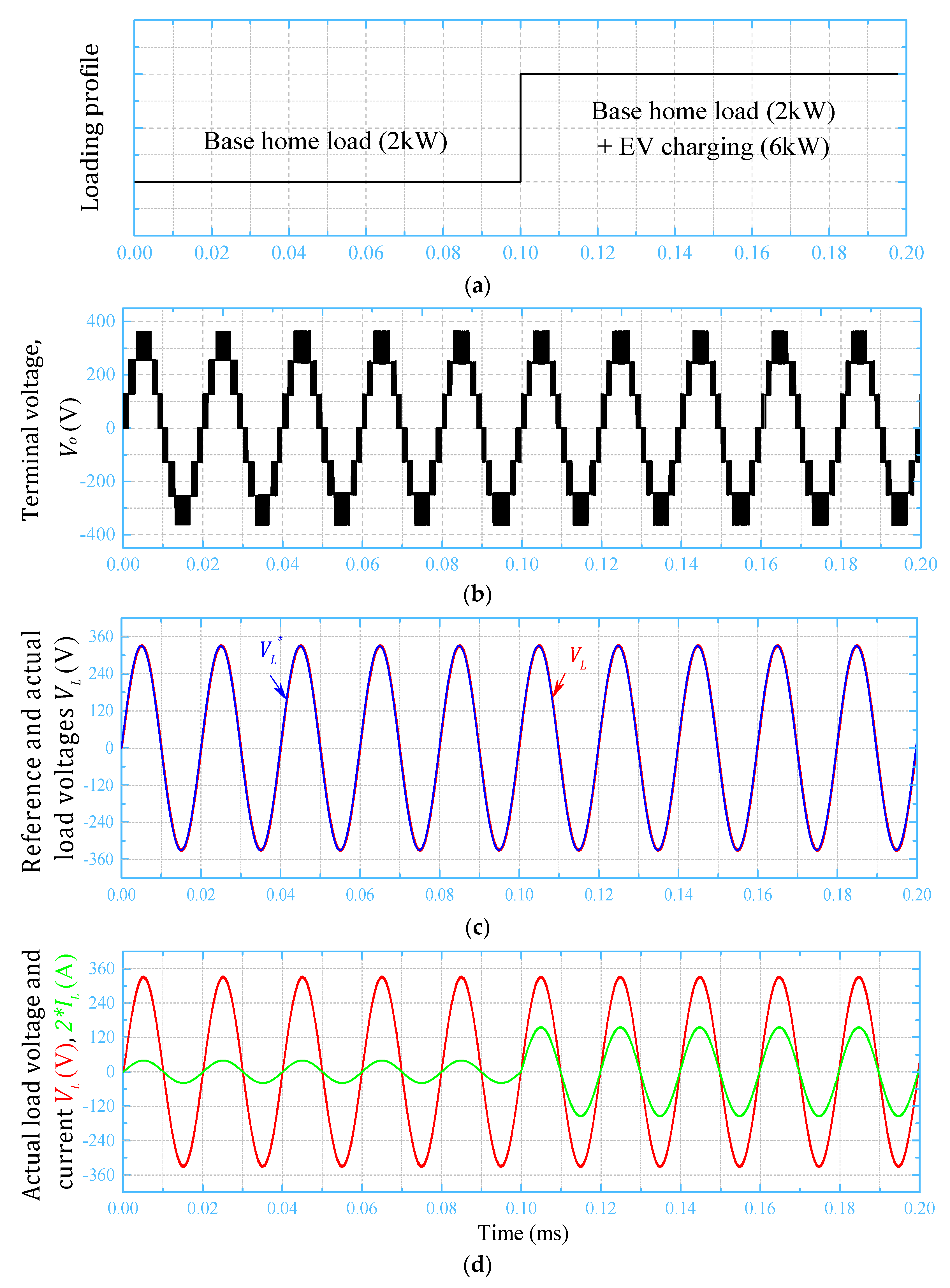
5. Simulation and Experimental Validations

5.1. Simulation Results

A MATLAB/Simulink model was developed for the entire PV system, including DC-DC BC with P&O MPPT and the proposed MLI with the associated controller. In this model, the main input source was a PV array and other sources were battery banks. The Canadian solar CS5P-220M PV module was considered in the model, which has the output characteristics at the standard test conditions listed in Table 3. The PV array consisted of five series modules (Ns = 5) and ten parallel modules (Np = 10), which showed the characteristics listed in Table 4. The system was tested under stand-alone as well as grid-integrated operation. For stand-alone operation, the load-voltage was sensed and compared with the reference value where the error signal was fed to a conventional PI controller to generate Ma. Similarly, for the grid-integration, the phase angle of the grid voltage as well as grid current were sensed for power factor correction. The measured and reference grid currents were compared and regulated using a PI controller, as indicated in Figure 6. In both cases, the output signal from PI controller was compared with the level-shifted carrier waveforms to generate the main switching signals and control periods (Qf, S1, …, S4). Then, the auxiliary circuit switching signals were derived for the 7-level inverter. The PV grid-tied system was tested under different solar irradiance, which varies from 1000 (W/m2) to 700 (W/m2) to validate the performance of MPPT technique under uniform as well as step-changed solar irradiance as a hard tracking condition [2].
Figure 7 shows the PV panel output current, voltage, and power with a step-variation in irradiance profile from 1000 W/m2 to 700 W/m2 to ensure MPPT controller stability at different irradiance conditions. The constant voltage profile in Figure 7c proves that the PV array operates efficiently at the MPP, regardless the fluctuations in irradiance profile. In addition, the extracted power at 1000 W/m2 matches the listed maximum power at the standard test conditions presented in Table 4. On the grid side, Figure 8 exhibits the inverter output voltage. The inverter terminal-voltage is a high-frequency modulated at 7-levels before the grid-current filter with its fundamental component is in-phase with the grid-voltage, as depicted Figure 8. Figure 9 exhibits the change in the grid-voltage, grid-injected current, and grid-injected power with step variation of irradiation. The grid-injected current is sinusoidal waveform and in-phase with the grid-voltage for unity power-factor operation of grid-integrated PV-system. To prove the robustness of the grid-tied controller with minimum error, the reference and actual grid currents are depicted in Figure 10. The actual grid-current tracks the reference current with minimum error, low settling time, and enhanced system response.
The Fast Fourier Transform (FFT) harmonic analysis of the grid-injected current and inverter terminal-voltage are portrayed in Figure 11. The grid current harmonic orders are compared with IEEE-1547 harmonic standard limit for Distributed Energy Resources (DER). The grid current THD is 3.75% and its harmonic orders are below the standard individual order limits as shown in Figure 11a. Also, the FFT harmonic spectrum of the inverter terminal multilevel voltage is portrayed in Figure 11b and its THD is 24.35%.
In addition, the grid integrated home/EV system is tested under uniform irradiance profile (fixed at 1000 W/m2) considering grid current pulsating change for EV charging, which considers base grid and home power of 3 kW and 2 kW, respectively, as depicted in Figure 12. Figure 12a shows the loading profile before and after EV charging connection and in case of the grid-integrated operation. The inverter multilevel output voltage with pulsating charging current of EV is shown in Figure 12b. The inverter terminal voltage has 7-levels even under load current/power variation. In addition, the grid voltage and load current based on the former loading profile is depicted in Figure 12c. Obviously, the base home and grid injected power are applied between staring time up to (0.1 s). Between the time intervals (0.1 and 0.2 s), the EV is connected to the grid for EV charging and the grid power is increased from 5 kW to 11 kW, as cleared in the grid pulsating current in Figure 12c.
For closed-loop load-voltage control of home/EV operation, the loading profile of the home/EV system considering home base load of 2 kW is depicted in Figure 13a. Figure 13b shows the 7-level terminal-voltage of the proposed inverter. Reference and actual load-voltages are portrayed in Figure 13c. Obviously, the actual load-voltage follows the reference value with reduced steady-state error and sinusoidal waveform with low THD for enhanced power-quality considering low passive elements. In addition, the load voltage and current waveforms, considering the loading profile in Figure 13a, are depicted in Figure 13d. The load current is sinusoidal waveform with reduced THD and unity power-factor operation. The FFT harmonic spectrum of the load current is analyzed in Figure 14. The THD of the load current is 2.3%, which enhances the power-quality of the load power that follows the IEEE-519 harmonic standard limits.

5.2. Experimental Results

An experimental prototype is built for the proposed MLI and the associated control to validate its performance. The proposed MLI is integrated and tested in a test platform considering the proper sinusoidal PWM switching strategy, as depicted in Figure 4. For simplicity, a DC supply is used to emulate the PV array, BC, and MPPT. Figure 15 shows the experimental prototype and the measured system parameters are listed in Table 5. The prototype consists of an input DC-source, two non-identical batteries, and the proposed MLI. The dc sources Vdc1 and Vdc2 at the input side of the experimental prototype have been implemented as ideal DC sources instead of batteries, which is acceptable given the large difference between time constants of batteries and converters. The main H-bridge inverter switches are implemented using IRFP264PBF MOSFETs and the auxiliary circuit switches are deployed using IGW50N65F4 IGBTs, for unidirectional power-flow, which are interfaced with Dspace DS-1103 controller via 6N137 gate-driver circuits. The SPWM switching technique is developed according to Table 1 and Figure 4. The switching-frequency of the proposed 7-level inverter is 10 kHz to synthesize the high-frequency modulated voltage at the inverter terminals. The proposed inverter is tested during stand-alone and grid-connected operations. In both cases, a conventional PI controller is used for error signal regulation to generate the modulation index to synthesize the inverter switching signals.
Figure 16 shows the measured terminal-voltage waveform of the proposed inverter. The inverter voltage realizes the seven levels like the simulation results. In addition, the proposed inverter is tested with a closed loop voltage control for stand-alone operation and the results are depicted in Figure 17. As noted, the actual voltage tracks the reference value with a small voltage error, which feeds the load with a sinusoidal current waveform, as indicated in Figure 17a. A small phase-shift is noticed between reference and actual load voltages due to the PI-controller steady state error [48], which has no effect on the converter control technique and its stability operation. FFT spectrum of the load voltage is displayed in Figure 17b, which shows a THD of 3.73%. The RMS values of load voltage, current, power, and efficiency of the proposed 7-level inverter are captured from the WT1800 power analyzer and presented in Figure 17c. The proposed inverter exhibits a high operating efficiency of 92.5% compared to most of the topologies presented in the literature.
To reveal the system validation of the proposed inverter for grid-integrated applications, the inverter was tested under grid-connected operation and the results are presented in Figure 18. The figure shows a comparison between the actual grid injected current and the reference value, which indicates the accuracy of the controller and inverter to track the reference current with a clean sinusoidal waveform. The THD of the measured grid current is 3.43%, which is within the standard limits defined by the IEEE-1547 standard for DER.

6. Conclusions

This paper has presented a new topology of a single-phase seven-level inverter as an interface for grid-integrated and stand-alone solar PV systems. The circuit configuration and operation principle of the proposed inverter have been presented in detail a long with the switching patterns and control strategy. A comparative study between the proposed inverter structure and the recent MLI topologies is enriched to reveal the features of the proposed inverter. The proposed MLI structure considers a reduced number of power switches, NC/L, and NAVG/Pole, which enhances the inverter operating efficiency and decreases its cost. Only seven switches have been utilized to synthesis voltage waveform of seven levels at the output terminals. The performance of the proposed inverter and associated control was investigated for grid-integrated and stand-alone PV systems based on simulation and experimental tests. The test platform includes a boost converter with MPPT control, which feeds the front-end of the proposed MLI. The results show that the proposed inverter exhibits an improved steady state response, and minimum settling time (i.e., 5 ms). THD of both voltage and current waveforms during grid-integration and stand-alone operations is 3.43%, which follows the IEEE-1547 harmonic standards for DER applications. In addition, the inverter offers a high operating efficiency of 92.86%, compared to most of the recently published topologies surveyed in this paper.

Author Contributions

Conceptualization, A.I.M.A.; methodology, A.I.M.A. and M.A.S.; software, A.I.M.A. and A.A.S.M.; validation, A.I.M.A., M.A.S. and A.A.S.M.; formal analysis, A.I.M.A.; investigation, A.I.M.A.; resources, A.I.M.A., M.A.S., and A.A.S.M.; data curation, A.I.M.A.; writing—original draft preparation, A.I.M.A.; writing—review and editing, A.I.M.A. and A.A.S.M.; visualization, A.I.M.A. and M.A.S. All authors have read and agreed to the published version of the manuscript.

Funding

This research received no external funding.

Institutional Review Board Statement

Not applicable.

Informed Consent Statement

Not applicable.

Data Availability Statement

Not applicable.

Acknowledgments

The National Renewable Energy Laboratory (NREL) is the current address for the third author only. NREL and the U.S. Department of Energy (DOE) did not contribute to this work.

Conflicts of Interest

The authors declare no conflict of interest.

Abbreviations

MaModulation index
NPSNumber of DC power supplies
NSNumber of switching devices
NDNumber of diodes
NCCapacitors Number
NTTransformers Number
NXNumber of other additional components
NPoleVoltage levels number per pole
NC/LNumber of components per level
NAVG/PoleAverage number of ON-switches per pole
Am, AcReference and carrier signal amplitudes
PnModes of operation
θnSwitching angle
PVPhotovoltaic
EVElectric vehicle
MLIMultilevel inverter
THDTotal harmonic distortion
EMIElectromagnetic interface
CHB-MLICascaded H-bridge MLI
NPC-MLINeutral Point Clamped MLI
FC-MLIFlying Capacitors MLI
SPWMSinusoidal pulse-width-modulation
MPPTMaximum power point tracking
BCBoost converter
SHE-PWMSelective harmonic elimination PWM
P&OPerturb and observe
FFTFast Fourier transform
DERDistributed energy resources

References

  1. Solangi, K.; Islam, M.; Saidur, R.; Rahim, N.; Fayaz, H. A review on global solar energy policy. Renew. Sustain. Energy Rev. 2011, 15, 2149–2163. [Google Scholar] [CrossRef]
  2. Ali, A.I.; Sayed, M.A.; Mohamed, E.E. Modified efficient perturb and observe maximum power point tracking technique for grid-tied PV system. Int. J. Electr. Power Energy Syst. 2018, 99, 192–202. [Google Scholar] [CrossRef]
  3. Sayed, M.A.; Mohamed, E.; Ali, A. Maximum Power Point Tracking Technique for Grid tie PV System. In Proceedings of the 7th International Middle-East Power System Conference, (MEPCON’15), Mansoura University, Dakahlia Governorate, Egypt, 15–17 December 2015. [Google Scholar]
  4. Ali, A.I.; Mohamed, E.E.; Sayed, M.A.; Saeed, M.S. Novel single-phase nine-level PWM inverter for grid connected solar PV farms. In Proceedings of the 2018 International Conference on Innovative Trends in Computer Eng. (ITCE), Aswan, Egypt, 19–21 February 2018; IEEE: Piscataway, NJ, USA, 2018; pp. 345–440. [Google Scholar]
  5. Youssef, A.-R.; Ali, A.I.; Saeed, M.S.; Mohamed, E.E. Advanced multi-sector P&O maximum power point tracking technique for wind energy conversion system. Int. J. Electr. Power Energy Syst. 2019, 107, 89–97. [Google Scholar]
  6. Feloups, C.E.; Ali, A.I.; Mohamed, E.E. Design of single-phase seven-level inverter with reduced number of switching devices for PV applications. In Proceedings of the 2017 Nineteenth International Middle East Power Systems Conference (MEPCON), Cairo, Egypt, 19–21 December 2017; IEEE: Piscataway, NJ, USA, 2017; pp. 817–822. [Google Scholar]
  7. Qiao, Q.; Zhao, F.; Liu, Z.; He, X.; Hao, H. Life cycle greenhouse gas emissions of Electric Vehicles in China: Combining the vehicle cycle and fuel cycle. Energy 2019, 177, 222–233. [Google Scholar] [CrossRef]
  8. Deb, S.; Tammi, K.; Kalita, K.; Mahanta, P. Impact of electric vehicle charging station load on distribution network. Energies 2018, 11, 178. [Google Scholar] [CrossRef] [Green Version]
  9. Ali, A.I.; Mohamed, E.E.; Youssef, A.-R. MPPT algorithm for grid-connected photovoltaic generation Syst. via model predictive controller. In Proceedings of the 2017 Nineteenth International Middle East Power Systems Conference (MEPCON), Cairo, Egypt, 19–21 December 2017; IEEE: Piscataway, NJ, USA, 2017; pp. 895–900. [Google Scholar]
  10. Van Der Kam, M.; van Sark, W. Smart charging of electric vehicles with photovoltaic power and vehicle-to-grid technology in a microgrid; a case study. Appl. Energy 2015, 152, 20–30. [Google Scholar] [CrossRef] [Green Version]
  11. Colmenar-Santos, A.; de Palacio-Rodriguez, C.; Rosales-Asensio, E.; Borge-Diez, D. Estimating the benefits of vehicle-to-home in islands: The case of the Canary Islands. Energy 2017, 134, 311–322. [Google Scholar] [CrossRef]
  12. Pan, L.; Zhang, C. An integrated multifunctional bidirectional AC/DC and DC/DC converter for electric vehicles applications. Energies 2016, 9, 493. [Google Scholar] [CrossRef] [Green Version]
  13. Ali, A.I.M.; Sayed, M.A.; Takeshita, T. Isolated single-phase single-stage DC-AC cascaded transformer-based multilevel inverter for stand-alone and grid-tied applications. Int. J. Electr. Power Energy Syst. 2021, 125, 106534. [Google Scholar] [CrossRef]
  14. Nabae, A.; Takahashi, I.; Akagi, H. A new neutral-point-clamped PWM inverter. IEEE Trans. Ind. Appl. 1981, IA-17, 518–523. [Google Scholar] [CrossRef]
  15. Ali, A.I.M.; Sayed, M.A.; Takeshita, T.; Hassan, A.M.; Azmy, A.M. A single-phase modular multilevel inverter based on controlled DC-cells under two SPWM techniques for renewable energy applications. Int. Trans. Electr. Energy Syst. 2021, 31, e12599. [Google Scholar] [CrossRef]
  16. Marchesoni, M.; Mazzucchelli, M.; Tenconi, S. A nonconventional power converter for plasma stabilization. IEEE Trans. Power Electron. 1990, 5, 212–219. [Google Scholar] [CrossRef]
  17. Vazquez, S.; Leon, J.I.; Carrasco, J.M.; Franquelo, L.G.; Galvan, E.; Reyes, M.; Sanchez, J.A.; Dominguez, E. Analysis of the power balance in the cells of a multilevel cascaded H-bridge converter. IEEE Trans. Ind. Electron. 2009, 57, 2287–2296. [Google Scholar] [CrossRef]
  18. Barros, J.D.; Silva, J.F.A.; Jesus, É.G. Fast-predictive optimal control of NPC multilevel converters. IEEE Trans. Ind. Electron. 2012, 60, 619–627. [Google Scholar] [CrossRef]
  19. Pouresmaeil, E.; Montesinos-Miracle, D.; Gomis-Bellmunt, O. Control scheme of three-level NPC inverter for integration of renewable energy resources into AC grid. IEEE Syst. J. 2011, 6, 242–253. [Google Scholar] [CrossRef]
  20. McGrath, B.P.; Holmes, D.G. Analytical determination of the capacitor voltage balancing dynamics for three-phase flying capacitor converters. IEEE Trans. Ind. Appl. 2009, 45, 1425–1433. [Google Scholar] [CrossRef]
  21. Zhang, L.; Waite, M.J.; Chong, B. Three-phase four-leg flying-capacitor multi-level inverter-based active power filter for unbalanced current operation. IET Power Electron. 2013, 6, 153–163. [Google Scholar] [CrossRef]
  22. Hinago, Y.; Koizumi, H. A single-phase multilevel inverter using switched series/parallel dc voltage sources. IEEE Trans. Ind. Electron. 2009, 57, 2643–2650. [Google Scholar] [CrossRef]
  23. Babaei, E. A cascade multilevel converter topology with reduced number of switches. IEEE Trans. Power Electron. 2008, 23, 2657–2664. [Google Scholar] [CrossRef]
  24. Li, Z.; Wang, P.; Li, Y.; Gao, F. A novel single-phase five-level inverter with coupled inductors. IEEE Trans. Power Electron. 2011, 27, 2716–2725. [Google Scholar] [CrossRef]
  25. Gupta, K.K.; Jain, S. Multilevel inverter topology based on series connected switched sources. IET Power Electron. 2013, 6, 164–174. [Google Scholar] [CrossRef]
  26. Babaei, E.; Laali, S.; Bayat, Z. A single-phase cascaded multilevel inverter based on a new basic unit with reduced number of power switches. IEEE Trans. Ind. Electron. 2014, 62, 922–929. [Google Scholar] [CrossRef]
  27. Vidales, B.; Monroy-Morales, J.L.; Rodríguez-Rodriguez, J.; Madrigal, M.; Torres-Lucio, D. A transformerless topology for a micro inverter with elevation factor of 1: 10 for photovoltaic applications. Int. J. Electr. Power Energy Syst. 2019, 109, 504–512. [Google Scholar] [CrossRef]
  28. Babaei, E.; Kangarlu, M.F.; Sabahi, M. Extended multilevel converters: An attempt to reduce the number of independent DC voltage sources in cascaded multilevel converters. IET Power Electron. 2014, 7, 157–166. [Google Scholar] [CrossRef]
  29. Ahmed, T.A.; Mohamed, E.E.; Youssef, A.-R.; Ibrahim, A.; Saeed, M.S.; Ali, A.I. Three phase modular multilevel inverter-based multi-terminal asymmetrical DC inputs for renewable energy applications. Eng. Sci. Technol. Int. J. 2020, 23, 831–839. [Google Scholar] [CrossRef]
  30. Ali, A.I.; Sayed, M.A.; Mohamed, E.E.; Azmy, A.M. Advanced single-phase nine-level converter for the integration of multiterminal DC supplies. IEEE J. Emerg. Sel. Top. Power Electron. 2018, 7, 1949–1958. [Google Scholar] [CrossRef]
  31. Ali, A.I.M.; Sayed, M.A.; Takeshita, T. Analysis and Design of High-Power Single-Stage Three-Phase Differential-Based Flyback Inverter for Photovoltaic Applications. In Proceedings of the 2020 22nd European Conference on Power Electronics and Applications (EPE’20 ECCE Europe), Lyon, France, 7–11 September 2020; IEEE: Piscataway, NJ, USA, 2020; pp. 1–8. [Google Scholar]
  32. Ali, A.I.M.; Sayed, M.A.; Takeshita, T. New Cascaded-Transformers Multilevel Inverter for Renewable Distribution Systems. In Proceedings of the 2020 IEEE Energy Conversion Congress and Exposition (ECCE), Detroit, MI, USA, 11–15 October 2020; IEEE: Piscataway, NJ, USA, 2020; pp. 3965–3971. [Google Scholar]
  33. Pereda, J.; Dixon, J. Cascaded multilevel converters: Optimal asymmetries and floating capacitor control. IEEE Trans. Ind. Electron. 2012, 60, 4784–4793. [Google Scholar] [CrossRef]
  34. Ali, A.I.; Mohamed, E.E.; Sayed, M.A.; Saeed, M.S.; Azmy, A.M. Design and Validation of a Single Phase Multilevel Inverter Utilizing Reduced Switches Number. In Proceedings of the 2018 Twentieth International Middle East Power Systems Conference (MEPCON), Cairo, Egypt, 18–20 December 2020; IEEE: Piscataway, NJ, USA, 2018; pp. 974–979. [Google Scholar]
  35. Wu, J.-C.; Wu, K.-D.; Jou, H.-L.; Chang, S.-K. Small-capacity grid-connected solar power generation system. IET Power Electron. 2014, 7, 2717–2725. [Google Scholar] [CrossRef] [Green Version]
  36. De, S.; Banerjee, D.; Gopakumar, K.; Ramchand, R.; Patel, C. Multilevel inverters for low-power application. IET Power Electron. 2011, 4, 384–392. [Google Scholar] [CrossRef]
  37. Kaliamoorthy, M.; Rajasekaran, V.; PraveenRaj, G. A novel single phase cascaded multilevel inverter for hybrid renewable energy sources. In Proceedings of the 2015 International Conference on Advanced Computing and Communication Systems, Haryana, India, 21–22 February 2015; IEEE: Piscataway, NJ, USA, 2015; pp. 1–10. [Google Scholar]
  38. Hassan, A.M.; Yang, X.; Ali, A.I.M.; Ahmed, T.A.; Azmy, A.M. A Study of Level-Shifted PWM Single-phase 11-Level Multilevel Inverter. In Proceedings of the 2019 21st International Middle East Power Systems Conference (MEPCON), Cairo, Egypt, 17–19 December 2019; pp. 170–176. [Google Scholar]
  39. Rao, S.N.; Kumar, D.A.; Babu, C.S. New multilevel inverter topology with reduced number of switches using advanced modulation strategies. In Proceedings of the 2013 International Conference on Power, Energy and Control (ICPEC), Dindigul, India, 6–8 February 2013; IEEE: Piscataway, NJ, USA, 2013; pp. 693–699. [Google Scholar]
  40. Mudadla, D.; Sandeep, N.; Rao, G.R. Novel asymmetrical multilevel inverter topology with reduced number of switches for photovoltaic applications. In Proceedings of the 2015 International Conference on Computation of Power, Energy, Information and Communication (ICCPEIC), Melmaruvathur, India, 22–23 April 2015; IEEE: Piscataway, NJ, USA, 2015; pp. 0123–0128. [Google Scholar]
  41. Ray, S.; Gupta, N.; Gupta, R.A. Hardware realization of proportional-resonant regulator based advanced current control strategy for cascaded H-bridge inverter based shunt active power filter. Int. Trans. Electr. Energy Syst. 2019, 29, e2714. [Google Scholar] [CrossRef]
  42. Sun, X.; Wang, B.; Zhou, Y.; Wang, W.; Du, H.; Lu, Z. A single DC source cascaded seven-level inverter integrating switched-capacitor techniques. IEEE Trans. Ind. Electron. 2016, 63, 7184–7194. [Google Scholar] [CrossRef]
  43. Noroozi, M.; Akbari, A.; Abrishamifar, A. A 5-level modified full-bridge stand-alone inverter with reduced number of switches. Int. Trans. Electr. Energy Syst. 2018, 28, e2638. [Google Scholar] [CrossRef]
  44. Ibrahim, S.A.; Palanimuthu, A.; Sathik, M.J. Symmetric switched diode multilevel inverter structure with minimised switch count. J. Eng. 2017, 2017, 469–478. [Google Scholar] [CrossRef]
  45. Jagabar Sathik, M.; Prabaharan, N.; Ibrahim, S.A.; Vijaykumar, K.; Blaabjerg, F. A new generalized switched diode multilevel inverter topology with reduced switch count and voltage on switches. Int. J. Circuit Theory Appl. 2020, 48, 619–637. [Google Scholar] [CrossRef]
  46. Ali, A.I.M.; Sayed, M.A.; Shawky, A.; Takeshita, T. Efficient Single-Stage Three-Phase Isolated Differential-Based Flyback Inverter with Selective Harmonic Compensation Strategy for Grid-Tied Applications. In Proceedings of the 2020 IEEE Applied Power Electronics Conference and Exposition (APEC), New Orleans, LA, USA, 15–19 March 2020; IEEE: Piscataway, NJ, USA, 2020; pp. 1778–1785. [Google Scholar]
  47. Ali, A.I.M. Techniques for Photovoltaic Generation; South Valley University: Qena Governorate, Egypt, 2017. [Google Scholar]
  48. Mohamed, A.A.; Metwally, H.; El-Sayed, A.; Selem, S. Predictive neural network based adaptive controller for grid-connected PV systems supplying pulse-load. Sol. Energy 2019, 193, 139–147. [Google Scholar] [CrossRef]
  49. Mohamed, A.A.; El-Sayed, A.; Metwally, H.; Selem, S.I. Grid integration of a PV system supporting an EV charging station using Salp Swarm Optimization. Solar Energy 2020, 205, 170–182. [Google Scholar] [CrossRef]
  50. Teodorescu, R.; Liserre, M.; Rodriguez, P. Grid Converters for Photovoltaic and Wind Power Systms; John Wiley & Sons: Hoboken, NJ, USA, 2011; Volume 29. [Google Scholar]
Figure 1. Circuit configuration of solar PV system integrated with the grid and EV loads via the proposed 7-level inverter.
Energies 14 02718 g001
Figure 2. Power circuit of the proposed 7-Level inverter.
Energies 14 02718 g002
Figure 3. Operational modes of the 7-level inverter to synthesize the multilevel output-voltage.
Energies 14 02718 g003
Figure 4. Switching strategy of the 7-Level PWM inverter.
Energies 14 02718 g004
Figure 5. Comparison between the proposed 7-level inverter and the recent topologies.
Energies 14 02718 g005
Figure 6. Control scheme of the grid connected PV system via the proposed 7-level inverter.
Energies 14 02718 g006
Figure 7. The PV panel current, voltage, and power.
Energies 14 02718 g007aEnergies 14 02718 g007b
Figure 8. Multi-Level inverter output voltage.
Energies 14 02718 g008
Figure 9. The injected current, voltage, and power variation. (a) Grid voltage and current; (b) Grid injected power.
Energies 14 02718 g009
Figure 10. The reference and actual injected currents of the seven-level inverter at irradiance variation.
Energies 14 02718 g010
Figure 11. FFT analysis of inverter output voltage and grid injected current; (a) grid current, and (b) inverter voltage.
Energies 14 02718 g011
Figure 12. Simulation results of the proposed 7-level inverter as level-2 EV charger (240 V, 3:6 kW); (a) loading profile, (b) multilevel output voltage, and (c) inverter voltage/pulsating current.
Energies 14 02718 g012
Figure 13. Simulation results of the proposed 7-level inverter for house loads voltage control (2 kW). (a) Load reference and actual voltages, (b) Load voltage and current.
Energies 14 02718 g013
Figure 14. House load current FFT harmonic spectrum at 2 kW.
Energies 14 02718 g014
Figure 15. A photograph of the experimental system.
Energies 14 02718 g015
Figure 16. Measurement of the 7-level inverter terminal-voltage at stand-alone load-voltage control.
Energies 14 02718 g016
Figure 17. Measurement of the 7-level inverter terminal-voltage at stand-alone load-voltage control.
Energies 14 02718 g017aEnergies 14 02718 g017b
Figure 18. The 7-level inverter experimental results under grid-tied current control.
Energies 14 02718 g018
Table 1. Output voltage levels according to switching states.
ComparisonAuxiliary Circuit SwitchingQ*Main Circuit SwitchingOutput-Voltage
QfQ1Q2S1S2S3S4VOut
VCar1 < VRef1 11 1 V d c
VCar2 < VRef 0
VCar3 < VRef 0
VCar1 < VRef0 11 1 2 3 V d c
VCar2 < VRef 0
VCar3 > VRef 1
VCar1 < VRef0 01 1 1 3 V d c
VCar2 > VRef 1
VCar3 > VRef 0
VCar1 > VRef0 0 1 10
VCar2 > VRef 0
VCar3 > VRef 0
VCar1 > VRef0 01 1 0
VCar2 > VRef 0
VCar3 > VRef 0
VCar1 < VRef0 0 11 1 3 V d c
VCar2 > VRef 1
VCar3 > VRef 0
VCar1 < VRef0 1 11 2 3 V d c
VCar2 < VRef 0
VCar3 > VRef 1
VCar1 < VRef1 1 11 V d c
VCar2 < VRef 0
VCar3 < VRef 0
Table 2. Comparison study of MLI topologies.
In Cited Paper:NPoleNPSNSNDNCNTNC/LNAVG/PoleTHD (%)Eff.
(%)
PWM Technique
ReferenceLevel
[35]74262002.53.64.894Fund. Frequency PWM
[14]531126207 SPWM
[17]
(a)
5
3280003.33 Fund. Frequency PWM
(b)
7
43120003.75 2.5--
(c)
9
541600048
[36]5321212008.67 MPC & SPWM
[20]
(a)
5
3140102 PSC-PWM
(b)
7
4160202.25
(c)
9
5180302.43
[21]531120506 5--3D-PWM
[37] 6094302.675.4 Fund. Frequency PWM
[38]
(a)
5
3260002.672.67388SPWM
(b)
7
4380002.75
(c)
9
54100002.84.4
[39]
(a)
5
3280003.333.33 SHE-PWM & SPWM
(b)
7
43100003.25 6.84--
(c)
9
54120003.25.2
[40] 5484003.2 4.24--Fund. Frequency PWM
[41] 3280003.3343.67--SHE-PWM & SPWM
[42] 41120203.754--90CPS-SPWM
[43] 3260002.6733.9--SPWM
[44] 4371002.7535.48--SPWM
[45] 3251002.6734.97--SPWM
[30]
(a)
7
43720033.334.384.5SPWM
(b)
9
54103003.42.8495
[15]
(a)
5
3251002.672.33388.5Two SPWM
(b)
7
4362002.752.752.990.3
(c)
9
5473002.83.2
Proposed MLI 7-level4171002.252.753.7392.86SPWM
Table 3. The characteristics of Canadian solar CS5P-220M PV module at STC.
Maximum Power (Pmpp)220 (W)
Voltage at MPP (Vmpp)47 (V)
Current at MPP (Impp)4.68 (A)
Open circuit voltage (Voc)58.8 (V)
Short circuit current (Isc)5.01 (A)
Table 4. The characteristics of PV array.
Maximum Power (Pmpp)11 (kW)
Voltage at MPP (Vmpp)235 (V)
Current at MPP (Impp)46.8 (A)
Open circuit voltage (Voc)294 (V)
Short circuit current (Isc)50.1 (A)
Table 5. Experimental system parameters.
Input Voltage (Vin)105 V
Grid voltage (Vg)70 V, 50 Hz
Load resistance (R)43 (Ω)
LC filter1 mH, 10 µF
AC line frequency50 Hz
Switching frequency (FSW)10 kHz
PI controller gains, KP, KI0.081 A/V, 200 rad s−1
Publisher’s Note: MDPI stays neutral with regard to jurisdictional claims in published maps and institutional affiliations.

