Article

Novel Single-Phase Grid-Tied NPC Five-Level Converter with an Inherent DC-Link Voltage Balancing Strategy for Power Quality Improvement

1
División de Estudios de Posgrado e Investigación, TNM Instituto Tecnológico de La Laguna, Torreón 27000, Mexico
2
School of Electrical and Information Engineering, University of the Witwatersrand, Johannesburg 2000, South Africa
3
Department of Electrical Engineering, École de Technologie Supérieure (ÉTS), Montreal, QC H3C 1K3, Canada
*
Author to whom correspondence should be addressed.
Energies 2021, 14(9), 2644; https://doi.org/10.3390/en14092644
Submission received: 24 March 2021 / Revised: 17 April 2021 / Accepted: 19 April 2021 / Published: 5 May 2021
(This article belongs to the Special Issue Control and Modeling of Power Converters and Inverters)

Abstract

:
This paper presents a novel single-phase grid-tied neutral-point-clamped (NPC) five-level converter (SPFLC). Unlike the literature on five-level NPC topologies, the proposed one is capable of inherently balancing the voltage of the DC-link split capacitors. For this purpose, a simple Multicarrier Phase Disposition (MPD) Pulse Width Modulation (PWM) technique is used, thus avoiding both complex modifications to the Space Vector Modulation (SVM) and offset voltage injections into the carrier based (CB) PWM, as commonly done in most conventional balancing algorithms. Bearing in mind that the proposed balancing strategy only requires measuring the capacitors’ voltages and the sign of the converter output current, it has a very low complexity. The developed strategy is not only straightforwardly implemented but is also very effective for obtaining symmetrical and undistorted voltage levels from the proposed multilevel converter, as well as for significantly improving the power quality of the SPFLC output voltage and, in turn, of the grid current. The simulation results obtained with MATLAB-SimPowerSystems as well as the experimental results obtained with the prototype built in the laboratory validate the topology of the proposed NPC five-level converter and the voltage balancing strategy, by showing a good performance under step-changes and exhaustive operating test conditions.

1. Introduction

Voltage source converters (VSCs) are the core of modern power electronics, which allow modifying the frequency, magnitude and phase of the input voltage with the aim of plant controlling or for electric energy flow regulation purposes. The multilevel VSCs (MC) require more complex modulation techniques than conventional two-level converters. However, they present several advantages such as lower total harmonic distortion (THD) of the output waveform, lower dv/dt stress of the power devices and lower electromagnetic interference (EMI) [1,2]. They can also achieve a high control performance with lower switching frequencies, which represent a significant reduction of the volume and cost of the required output passive filter, as well as lower losses equivalent to an overall higher efficiency [3].
Over the past years, various topologies of MC have been proposed, e.g., NPC [4,5,6] flying capacitor (FC) [7] and cascaded H-bridge (CHB) [8]. The NPC type is very attractive because all its output voltage levels are obtained from a single DC source, whereas the CHB topology has the drawback of requiring an isolated DC source per cell [9]. In contrast with FC, NPC does not have a limitation for operating at low switching frequencies and does not need precharging of the capacitors. Nevertheless, the NPC topology requires special techniques for compensating the inherent DC-link split capacitors’ unbalancing problem [10,11,12]. In single-phase five-level NPC converters, this issue can be avoided by using two isolated DC voltage sources instead of capacitors, but such a solution requires more components, which implies a higher cost and a bigger system complexity [13,14].
The simplified bridge five-level NPC topology (SBFLC) [15], hereinafter named conventional topology, consists of two legs; the first leg comes from a two-level converter and the second one from a three-level NPC converter [16,17]. This simplification advantageously reduces the number of components, but inconveniently eliminates the switching combinations of the redundant vectors, thus becoming incapable of compensating the inevitable voltage unbalancing phenomenon. Its effect can be reduced by fairly increasing the capacitance of the DC-link split capacitors, but at the expense of their larger size and cost [18].
Unlike the SBFLC topology, the full-bridge five-level NPC topology (FBFLC) is capable of balancing the split capacitors’ voltage [19,20]. For such purpose, different methods have been developed. In [21], the balancing strategy is based on injecting an offset voltage (OVI) into the carrier-based PWM, whereas [22] adopts a modified SVPWM algorithm and [23] utilizes an SVPWM segment-based modulation strategy. With the same aim, some other algorithms have been proposed, e.g., a nonlinear control technique [24], a neutral point current prediction [25] or varying the hybrid discontinuous PWM ratio with a PI controller [26].
In the present work, the authors propose a novel single-phase NPC five-level converter (SPFLC) based on a topology capable of inherently balancing the voltage of the DC-link split capacitors. Unlike [21,22], the proposed balancing strategy does not require either modifying the SVM or injecting offset voltages into the CBPWM; it uses a simple MPDPWM modulation technique [27,28], thus properly merging simplicity with functionality. Furthermore, given that the proposed balancing technique only requires measuring the capacitors’ voltages and the sign of the converter output current for selecting the appropriate compensating switching vector from a Look-Up Table (LUT), it has a much lower complexity than all of the strategies presented in [20,21,22,23,24,25,26]. It is also important to remark that, in contrast with [23], the appropriate switching vector selected for carrying out the balancing compensation remains the same during the whole switching period T s w .
The developed balancing strategy not only is straightforwardly implemented; it is also very effective for significantly improving the power quality of the proposed NPC multilevel converter output voltage and, in turn, of the grid current.
This paper is organized as follows: Section 2 describes the topology details of the proposed SPFLC, its current flowing paths for all switching states as well as the voltage balancing strategy of the DC-link split capacitors. Section 3 presents the vector control in the d q reference frame of the proposed grid-tied SPFLC. Section 4 shows the simulation results obtained with MATLAB-SimPowerSystems, whereas the experimental results obtained in laboratory, including a detailed power quality analysis are presented in Section 5. Section 6 provides the discussion and future research directions. Finally, the conclusions and some important remarks are given in Section 7.

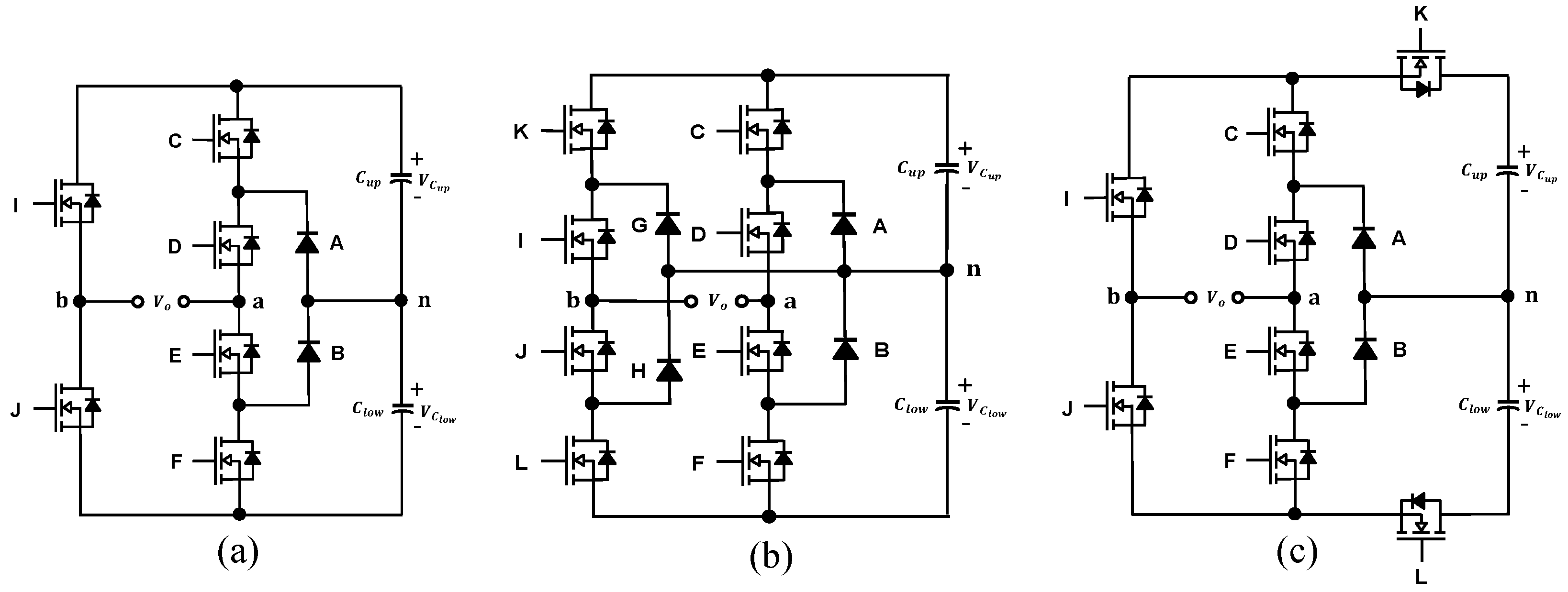
2. Proposed Single-Phase NPC Five-Level Converter

Figure 1 shows three different topologies of single-phase NPC five-level converters, i.e., the conventional simplified-bridge (SB), the full-bridge (FB) and the proposed one. It can be noted that the conventional topology consists of six switches, two neutral clamping diodes and two DC-link split capacitors, whereas the proposed topology has, in addition to these components, two more switches, i.e., it has a total of eight. However, with these two extra switches, the proposed converter advantageously becomes capable of inherently balancing the capacitors’ voltage. In contrast with the FBFLC, the proposed converter has two less clamping diodes and its balancing strategy does not require neither modifying the SVM or the CBPWM; nor does it depend on compensation closed loops or gain tuning. Table 1 shows a comparison of the three topologies in terms of the number of components and the voltage balancing characteristics.
On the other hand, for example, in the SB topology, only three switches stand with either half or even full DC bus voltage; this issue represents a serious inconvenience of the power devices’ stress. Unlike this conventional topology [15,16,17,18] and the FB topology [20,21,22,23,24,25,26], the proposed one has an equivalent of four and six switches at each leg, respectively. According to the switching state, the full DC bus voltage is shared among five switches, whereas half of the DC bus voltage is shared among either four or at least three switches, depending on the active state for the voltage balancing purposes. It is important to remark that this feature inherently represents the advantage of having a lower stress on the switching devices, thus making more feasible the use of MOSFETs instead of IGBTs. The MOSFETs for high power applications are not only less costly than IGBTs but are also capable of working at higher frequencies and more efficiently [10].

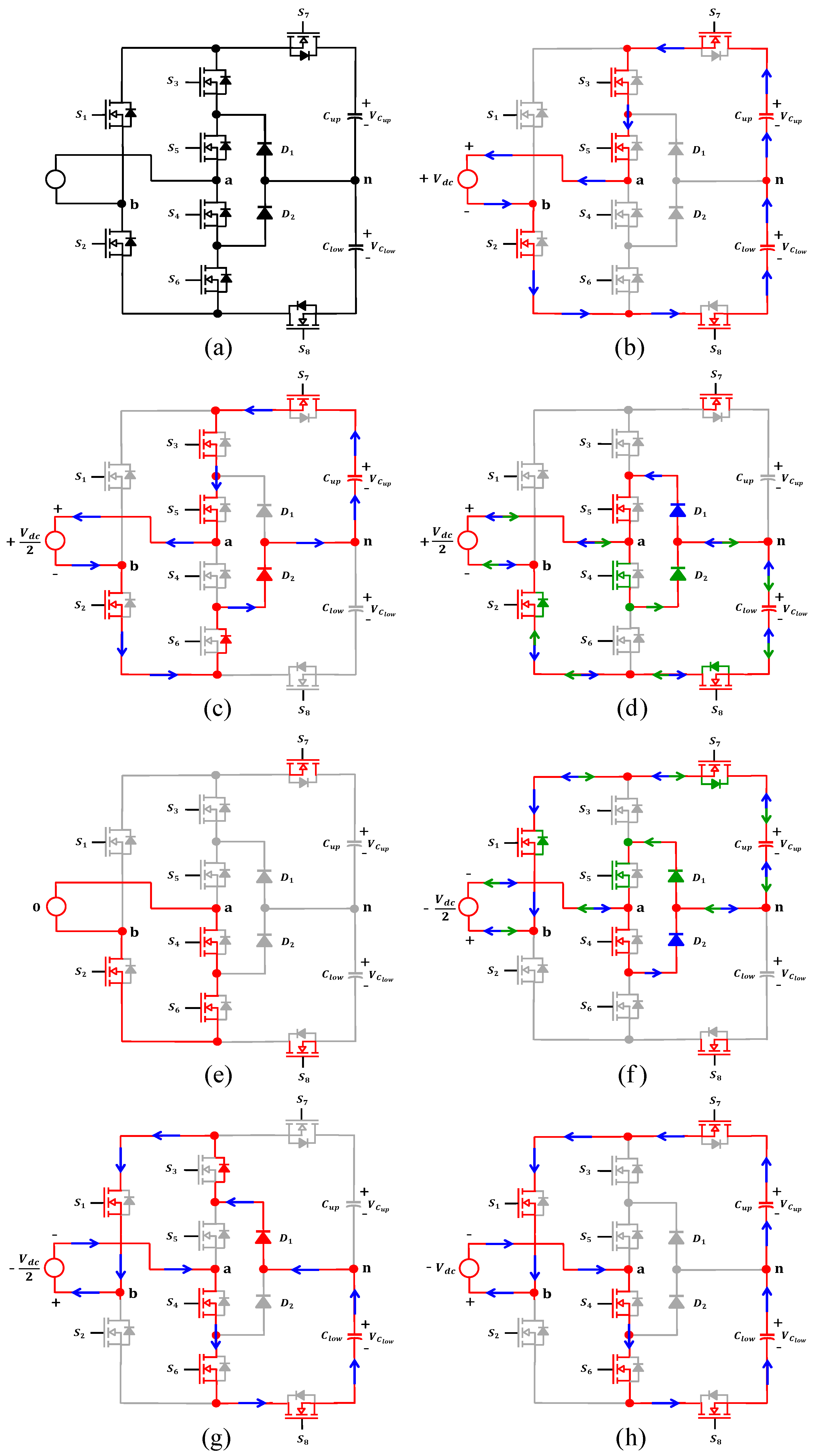
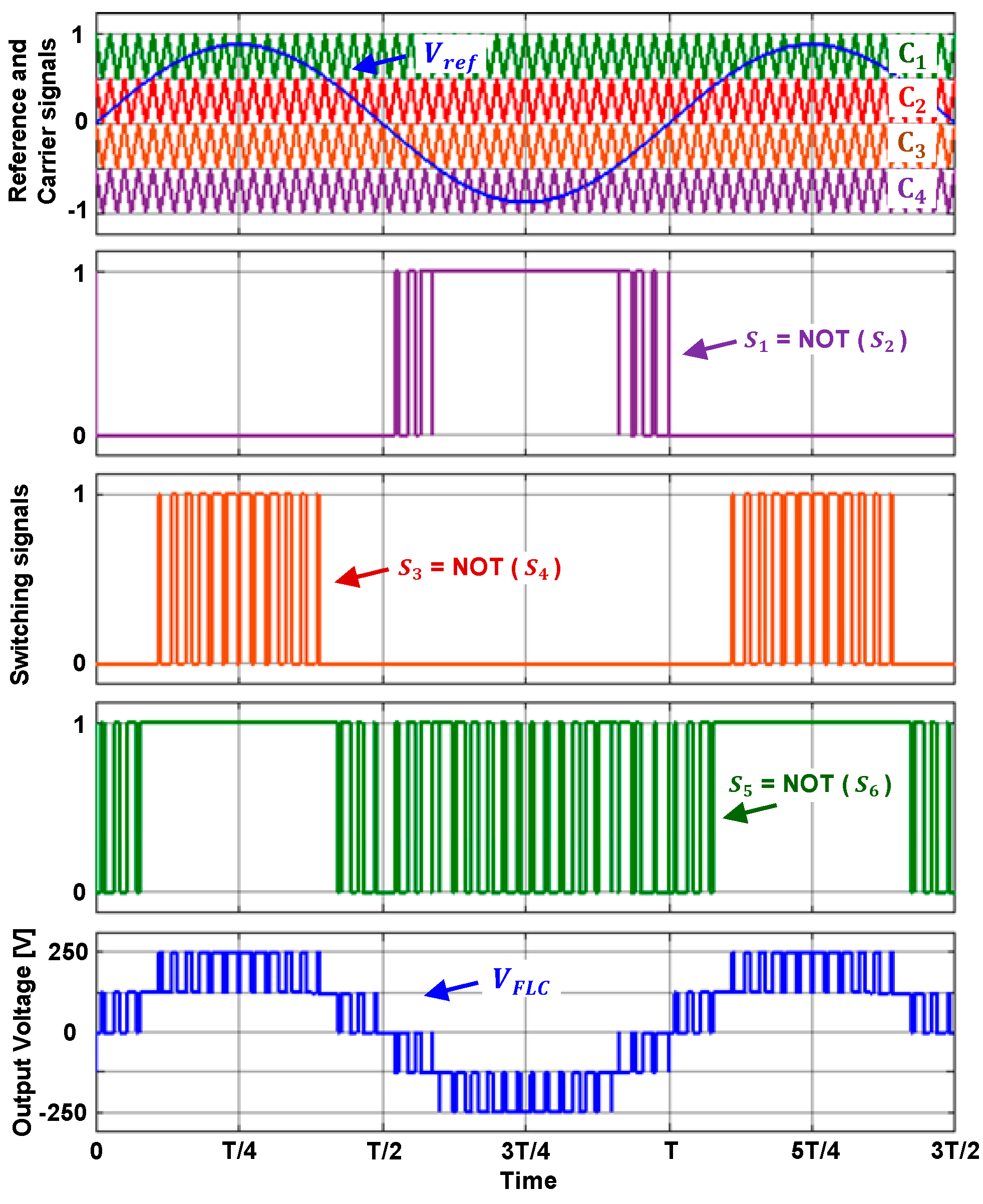
Current Flowing Paths of Proposed SPFLC and Voltage Balancing Strategy of DC-Link Split Capacitors

Figure 2 shows the current flowing paths for the seven switching states of the proposed single-phase five-level converter. The state of the eight switches at each switching state, the resulting output as a function of the DC-link voltage as well as the voltage balancing strategy are summarized in Table 2. According to the power electronic circuits of Figure 2b,h, it can be observed that in the respective states 1 and 5, the neutral point n remains disconnected from the midpoint path of the clamping diodes, thus leaving C u p and C l o w alone in series. Given that the same current flows through them, both are equally charged/discharged and thus, in such cases, there is no voltage unbalance problem. In state 3 (Figure 2e), there is no current path with any of the capacitors, therefore, their initial voltages are kept the same and no charge/discharge occurs. For each of the remaining states, i.e., 2 U (Figure 2c), 2 L (Figure 2d), 4 U (Figure 2f) and 4 L (Figure 2g), there exists a current path that involves only one of the two capacitors. Given that it will be charged/discharged while the other one stays disconnected and keeps the same initial voltage, an unbalance arises between them. By taking into account the sign of the SPFLC output current i F L C as well as the capacitors’ unbalance voltage V defined as V C u p V C l o w it is possible to maintain the voltage of both capacitors very close to each other. As described in Table 2, if the balancing algorithm is activated during the + V d c / 2 output voltage and V 0 and i F L C 0 , then the switching state 2 U has to be applied to the eight switches S 1 , S 2 S 8 , whereas if the balancing algorithm is deactivated or well-activated (it does not matter), but with a combination of V and i F L C that is not greater than or equal to zero, then the switching state 2 L has to be selected. Similarly, for carrying out the voltage balancing during the V d c / 2 output voltage, the algorithm chooses between the switching states 4 U and 4 L according to its activation/deactivation and also considering the conditions in which V < 0 and i F L C < 0 . By following Table 2, the proposed voltage balancing strategy for the split capacitors is capable of properly keeping the average neutral current around zero, even under step-changing conditions. Note that with the aim of contributing to reduce the switching losses during the voltage balancing, S 7 remains on in states 2 U/2 L, whereas S 8 remains on in states 4 U/4 L, respectively. Besides, irrespective of whether the balancing algorithm is active or not, both of these switches are always on in state 3.
Figure 3 shows the signals of the Multicarrier Phase Disposition PWM modulation strategy [27,28]. The reference or modulating signal and the triangular carrier signals, as well as the switching pattern and the resulting output voltage from the proposed SPFLC can be observed. This graph was obtained with the voltage balancing algorithm deactivated ( S 7 = S 8 = 1 ) and without current flow.

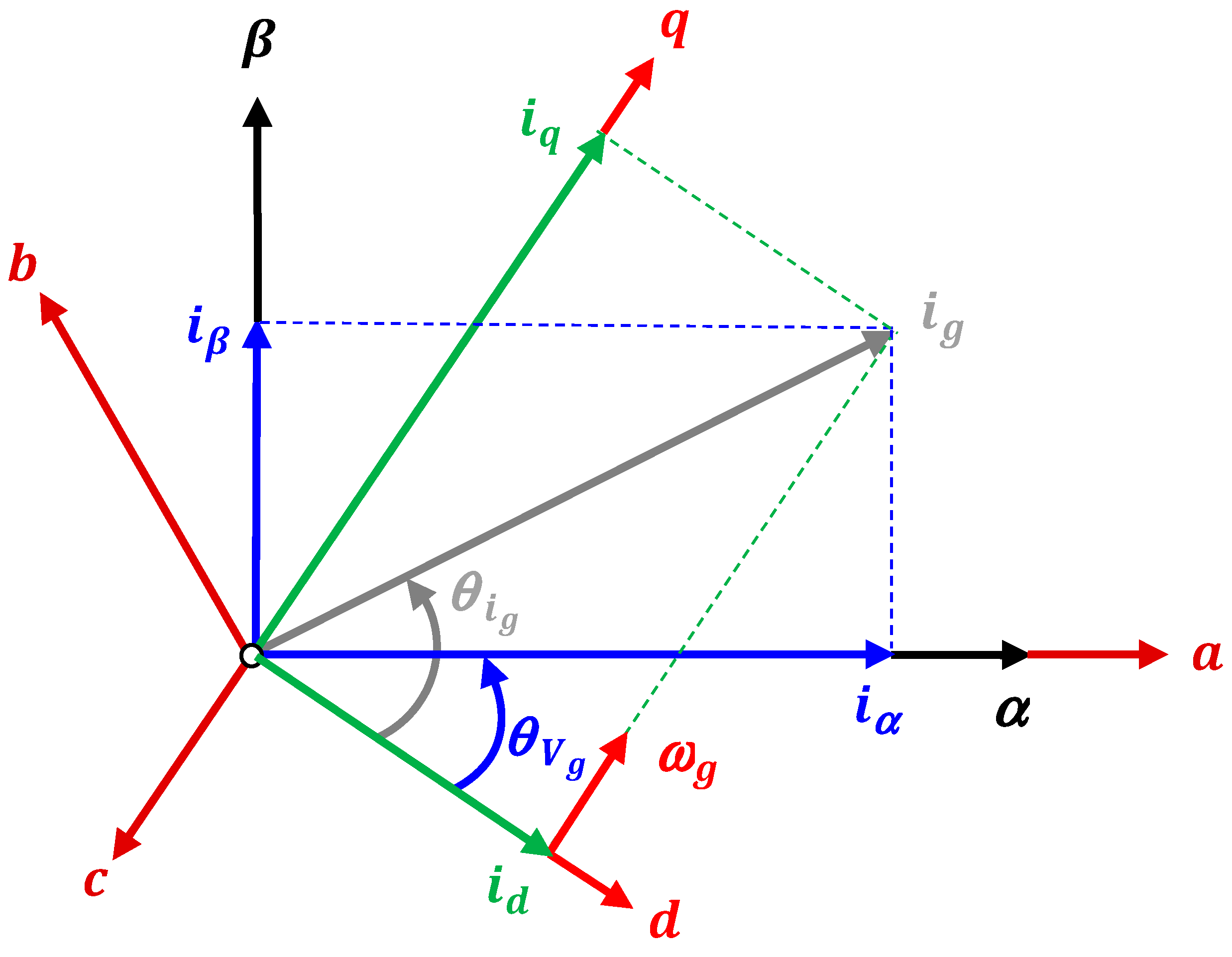
3. Vector Control of Proposed Grid-Tied SPFLC

Figure 4 shows the block diagram of the implemented current vector control strategy in the d q rotating coordinates for the proposed single-phase five-level converter connected to the grid through an R L line. It can be noted that the voltage component is the only control signal fed into the MPDPWM block, whereas the β component is simply disregarded [29]. Considering the equivalent three-phase representation from the one-line single-phase power system shown in Figure 4 and applying the Kirchhoff voltage law to the resulting circuit, the following equation in the a b c stationary frame is obtained [29]:
L L d i a b c d t + R L i a b c + V F L C a b c V g a b c = 0
In turn, the direct Clarke transformation allows representing (1) in the two phases of α β stationary frame as:
L L d i α β d t + R L i α β + V F L C α β V g α β = 0
where the three- and two-phase grid current vectors are i a b c = [ i a   i b   i c ] T and i α β = [ i α   i β ] T , respectively. After applying the direct Park transform (5) to (2), the expanded equations in the d q rotating reference frame are given by [29]:
L L d i d d t + R L i d   ω g L L i q + V F L C d V g d = 0
L L d i q d t + R L i q + g L L i d + V F L C q V g q = 0
In order to decouple the d - and q -axis current controllers, the resulting coupling factors ω g L L i q and ω g L L i d have to be subtracted in the control loops, as shown in Figure 4. The simulation results presented in Section 4 have been obtained with k p = 20 and k i = 80 for both d and q loops, whereas the experimental results presented in Section 5 have been obtained with k p = 3 and k i = 125 , respectively. The details about the design procedure of the linear PI controllers, considering the current control loops and the resulting transfer functions, can be found in [29]. The vector control of the single-phase grid current is based on the space vector diagram shown in Figure 5.
Besides, the direct P and inverse P 1 Park matrices used for transforming between the stationary coordinates α β and the rotating coordinates d q are defined as follows.
[ i d i q ] = [ P ] [ i α β ] = [ c o s ( θ V g ) s i n ( θ V g ) s i n ( θ V g ) c o s ( θ V g ) ] [ i α i β ]
[ i α i β ] = [ P 1 ] [ i d q ] = [ c o s ( θ V g ) s i n ( θ V g ) s i n ( θ V g ) c o s ( θ V g ) ] [ i d i q ]
where the product of these transformation matrices satisfies the property of giving the identity matrix I as
[ P ] [ P 1 ] = [ P 1 ] [ P ] = [ 1 0 0 1 ] = [ I ]
The grid voltage phase θ V g used in Park transforms and the beta grid current component i g β have been obtained by using the PLL, developed by Ziarani et al. [30].

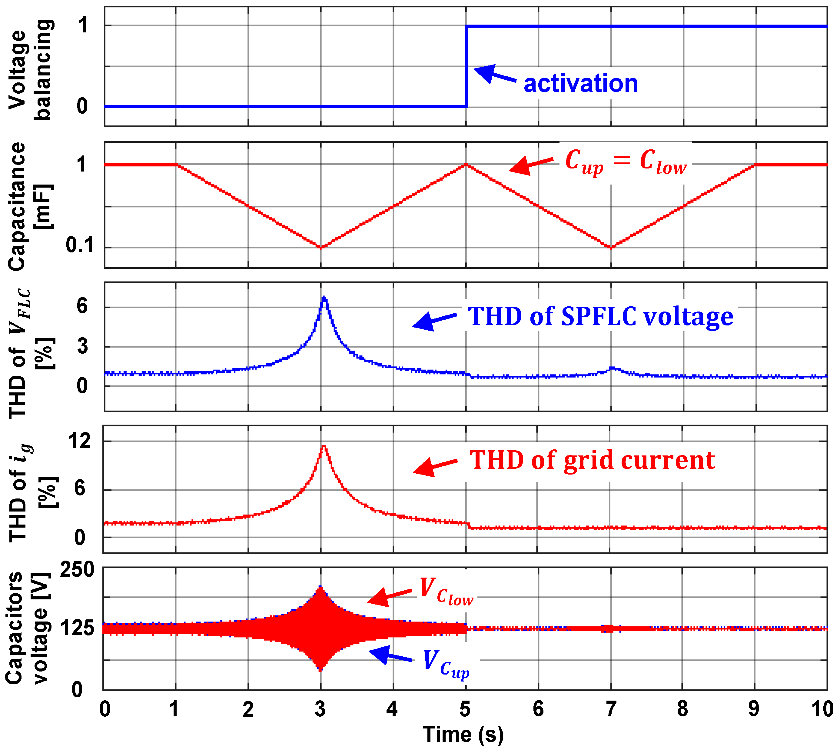
4. Simulation Results

In order to validate the proposed grid-tied SPFLC, it was simulated in MATLAB-SimPowerSystems. Figure 6, Figure 7, Figure 8, Figure 9 and Figure 10 show the results obtained from different tests under various operating conditions.
In Figure 6, the response of the grid current control as well as of the strategy for balancing the voltage of the DC-link split capacitors in the proposed five-level converter, during steady state of the d q grid currents, can be observed. It is noteworthy how from half the time scale, i.e., t = 0.15 ns, when the voltage balancing is activated, the voltage unbalance of capacitors is fairly well compensated. In a very short-time, lower than 5 ms, the voltage of both capacitors practically achieves an overlapping at the constant level of V d c / 2 . Note also how the negative slope at state 2 and the positive slope at state 4 of the SPFLC output voltage are properly corrected in a similar way, thus becoming a symmetrical and high-quality waveform. Figure 6 further shows the good performance of Ziarani’s PLL for deriving the grid current β component and, in turn, of the resulting vector control for duly regulating the direct i d and quadrature i q currents to zero and 10 A, respectively. It is important to remark how the component i g β properly lags the i g α grid current by 90°, while it is accurately maintained out-of-phase with the grid voltage V g . During this test, the capacitance of the upper and lower DC-link split capacitors has remained constant at C u p = C l o w = 200 μF.
Figure 7 shows the performance of the voltage balancing strategy and the vector control technique for the proposed grid-tied SPFLC during a step-change of the quadrature grid current component i q * from 5 A to 10   A and then returned back to 5 A. Thanks to the decoupling of the d q current loops, the d axis current component properly remains at zero during all the simulation time, in spite of the step-changes carried out in the q axis. It can be observed how the voltage unbalance of the DC-link split capacitors increases with i q . However, it is quite well-compensated after the activation of the balancing strategy at t = 0.15 s.
Figure 8 shows the performance of the voltage balancing strategy and the vector control for the proposed SPFLC during a grid voltage sag/swell. In this test, the peak value V p k of the grid voltage was step-changed from 220 V to 180 V, thus representing a sag of 18%. After 50 ms, V p k is returned back to 220 V, equivalent to a swell of around 22%. It can be observed that the voltage unbalance is inversely proportional with V p k . However, thanks to the balancing strategy activated at t = 0.15 s, the voltage unbalance is fairly well-regulated, thus accurately maintaining the voltage of split capacitors at 125 V from half the time scale. The good performance of the vector control for maintaining a constant and undisturbed grid current component during the step-changes of V p k is noteworthy.
Figure 9 shows the performance of the voltage balancing strategy and the vector control technique for the proposed SPFLC during a DC bus voltage variation. At t = 0.05 s, the magnitude of V d c was step-changed from 250 V to 300 V, thus representing an increment of 20%. Later, at t = 0.1 s, V d c is returned to 250 V, equivalent to a decrement of around 17%. It can be observed that the voltage unbalance increases with V d c . However, the voltage balancing strategy activated at half the time scale is capable of properly regulating the voltage of the split capacitors at V d c /2. The negligible influence of the DC bus voltage changes on the d q current components is also noteworthy.
Figure 10 shows the dynamic response of the voltage balancing strategy and the vector control for the proposed grid-tied SPFLC during a sweep of the capacitance C u p and C l o w of the DC-link split capacitors. In this test, C u p = C l o w was varied following a triangular waveform, with peak values of 1 mF and 100 μF. It can be observed how the voltage unbalance as well as the THD of the output voltage V F L C from the SPFLC and, in turn, the THD of the grid current i g increase nonlinearly with the linear reduction of such capacitance. Therefore, the maximum values of voltage unbalance and harmonic distortion occur at t = 3 s and t = 7 s, i.e., the points of minimum capacitance. It is noteworthy how after the activation of the voltage balancing strategy at half the time scale, i.e., t = 5 s, the voltage unbalance decreases from 125 V ± 85 V to only 125 V ± 7 V, whereas the maximum THD of V F L C and i g reduces from 6.9% and 11.4% to only 1.5% and 1.4%, respectively. This considerable reduction in the harmonic content of V F L C and i g clearly shows the significant power quality improvement achieved, thanks to the inherent capability of the proposed SPFLC for properly balancing the voltage of DC-link split capacitors. During this test, the direct and quadrature grid current components have been maintained constant at i d * = 0 and i q * = 10   A .

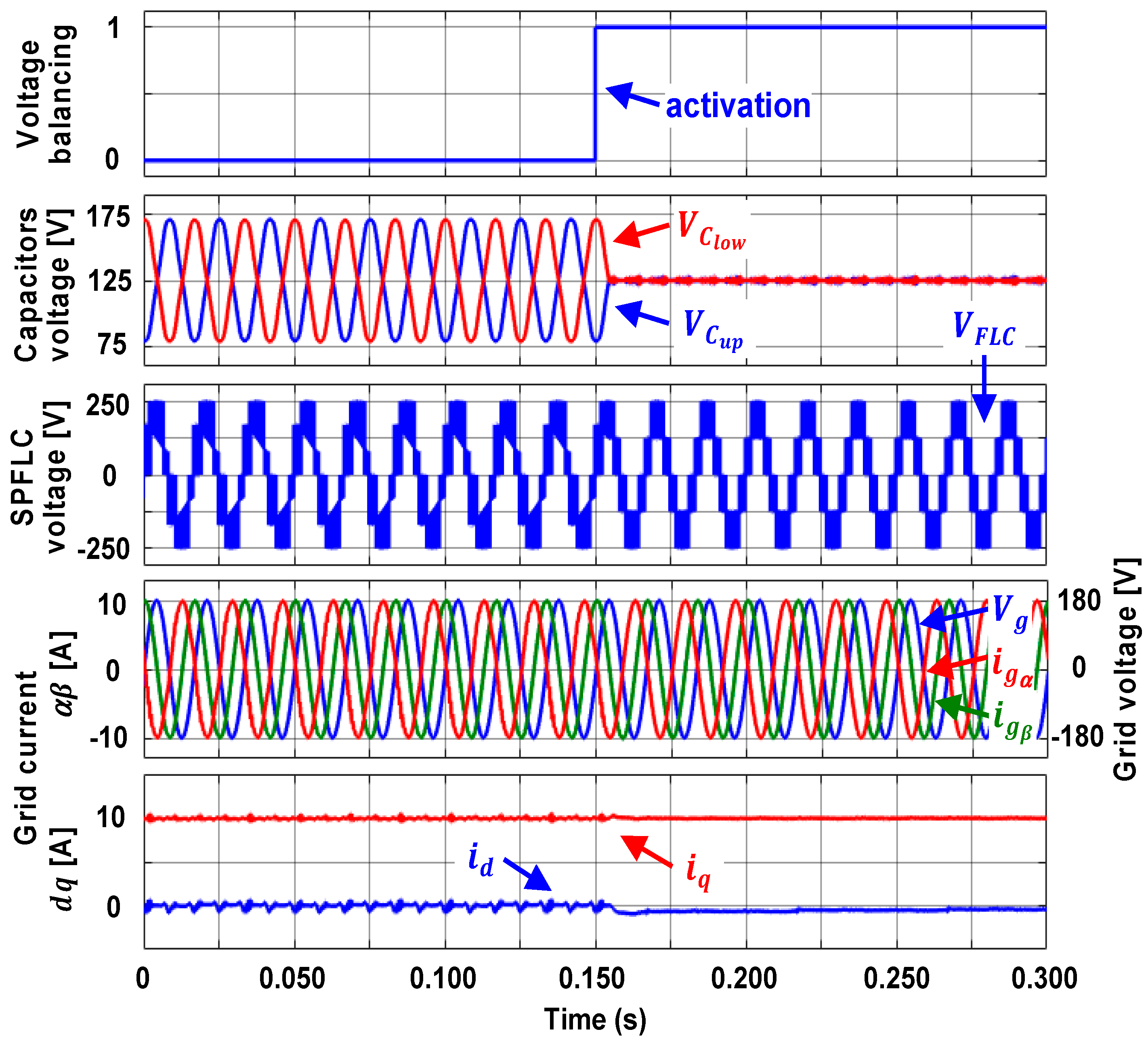
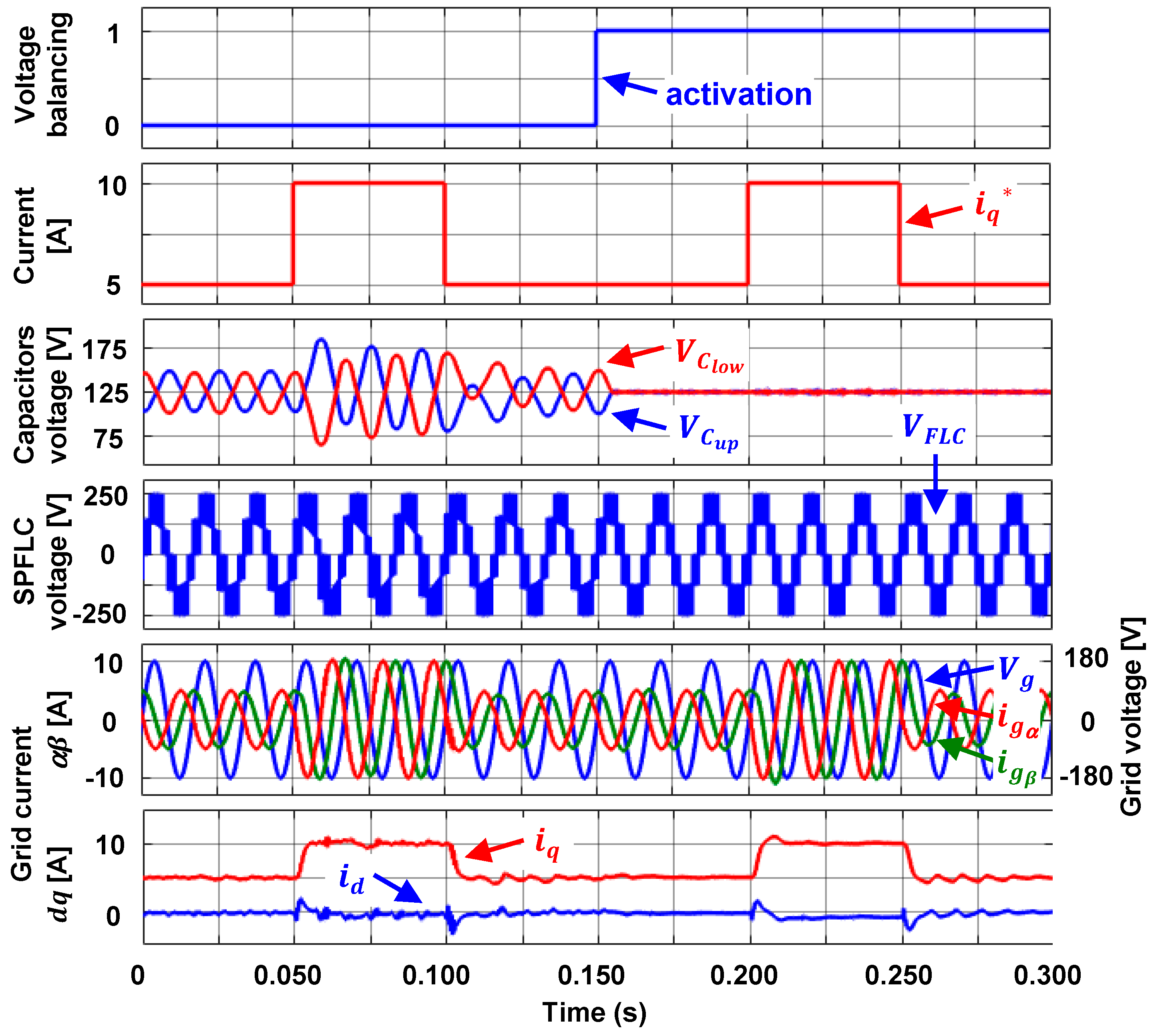
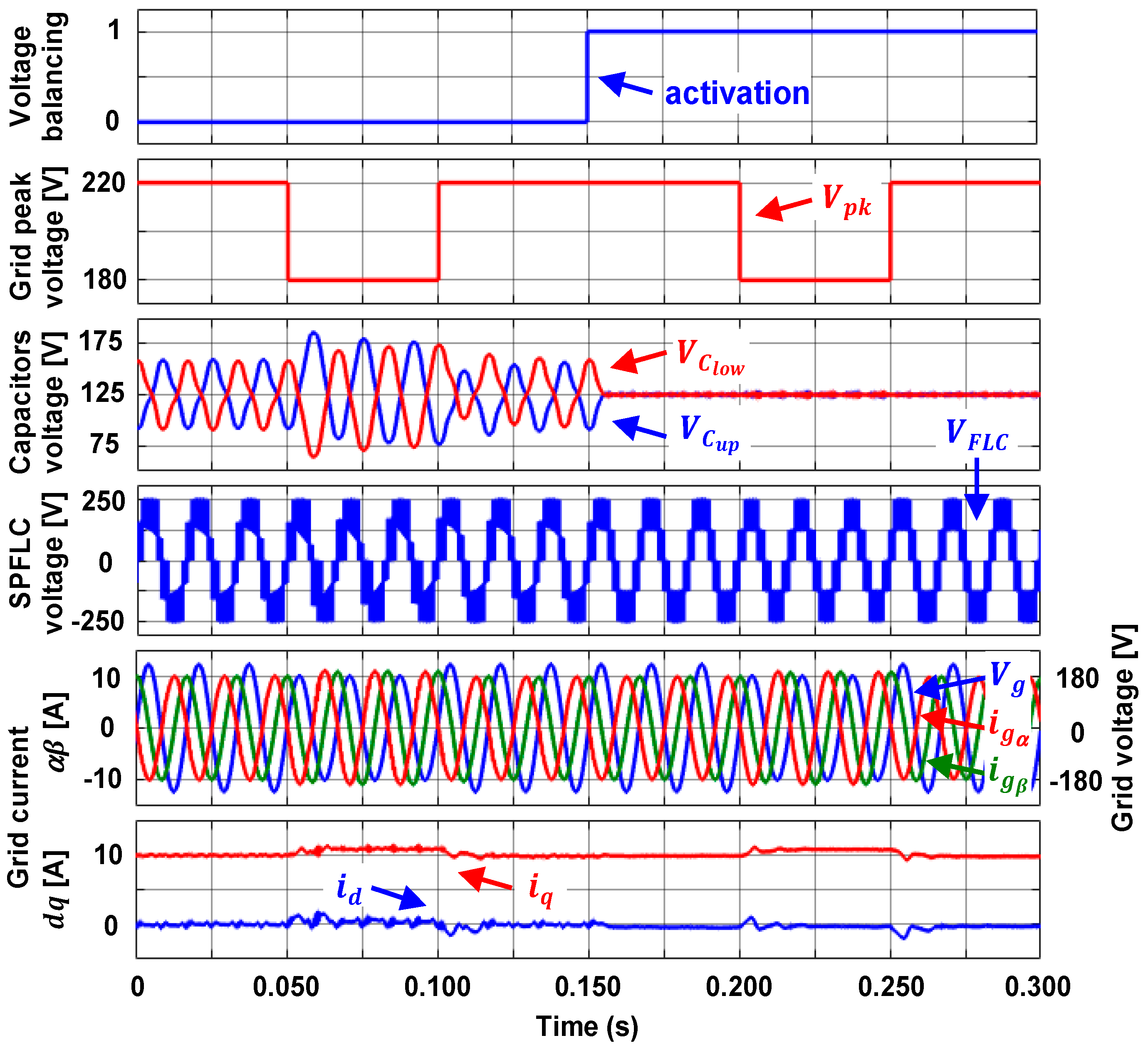
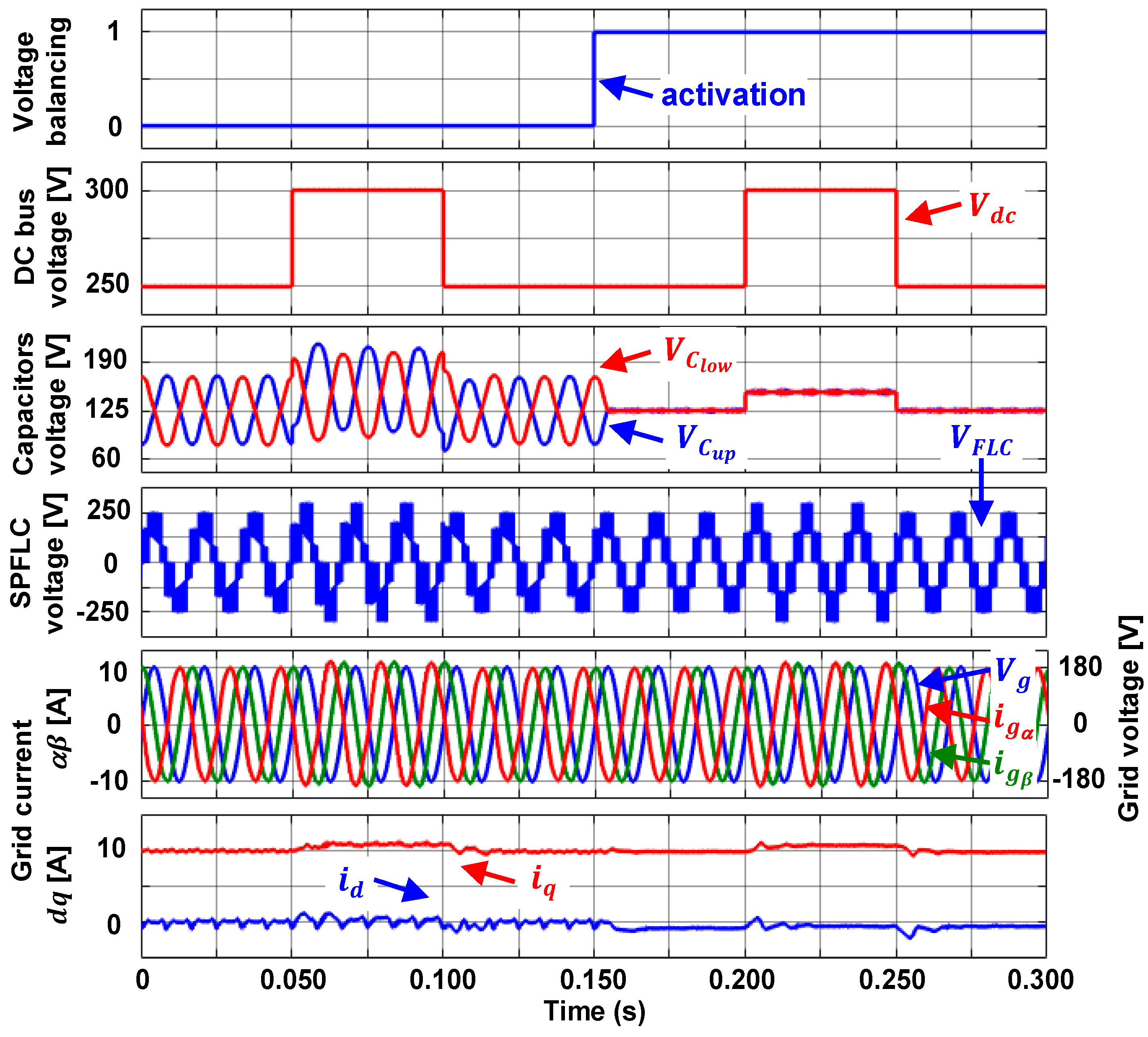
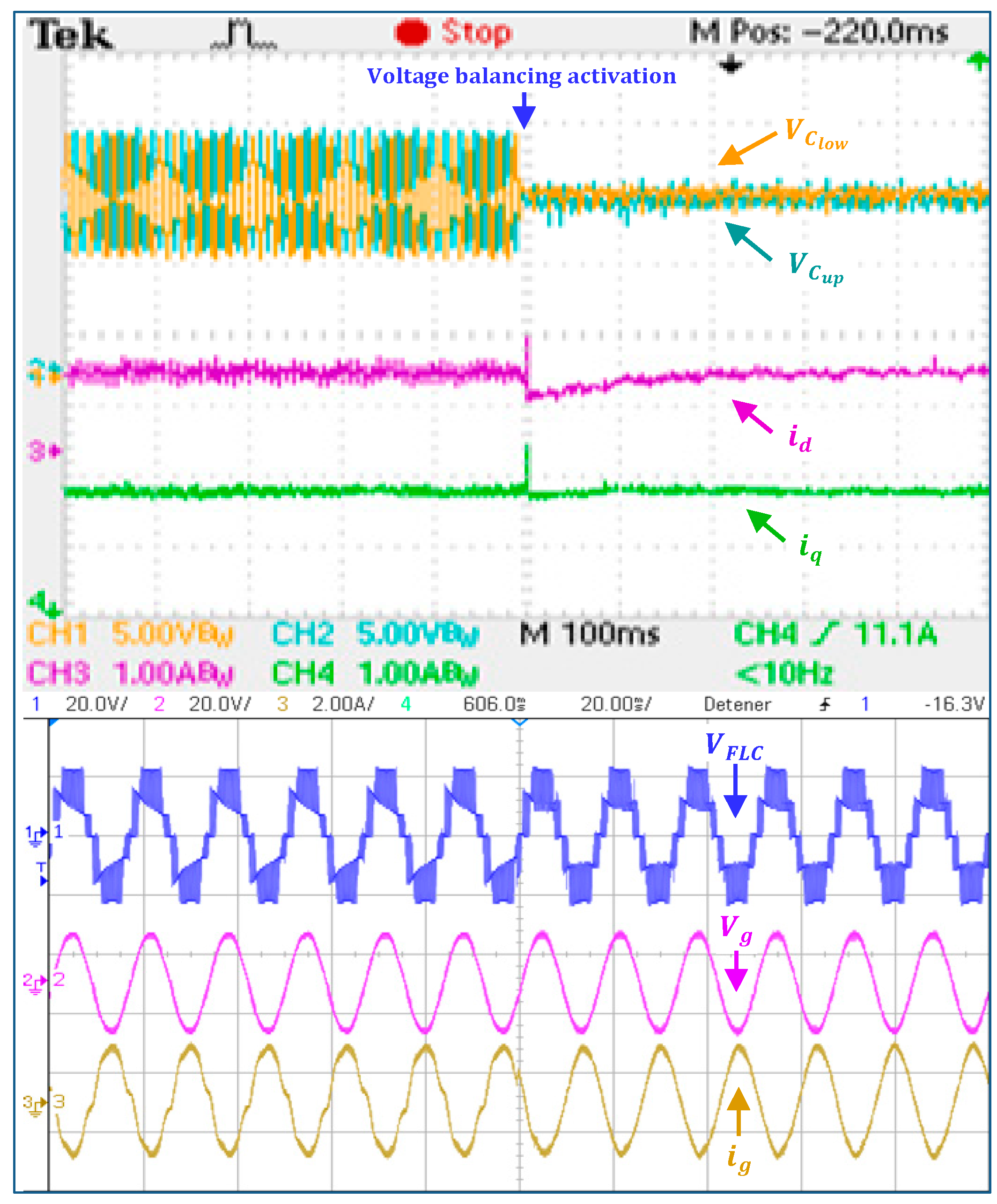
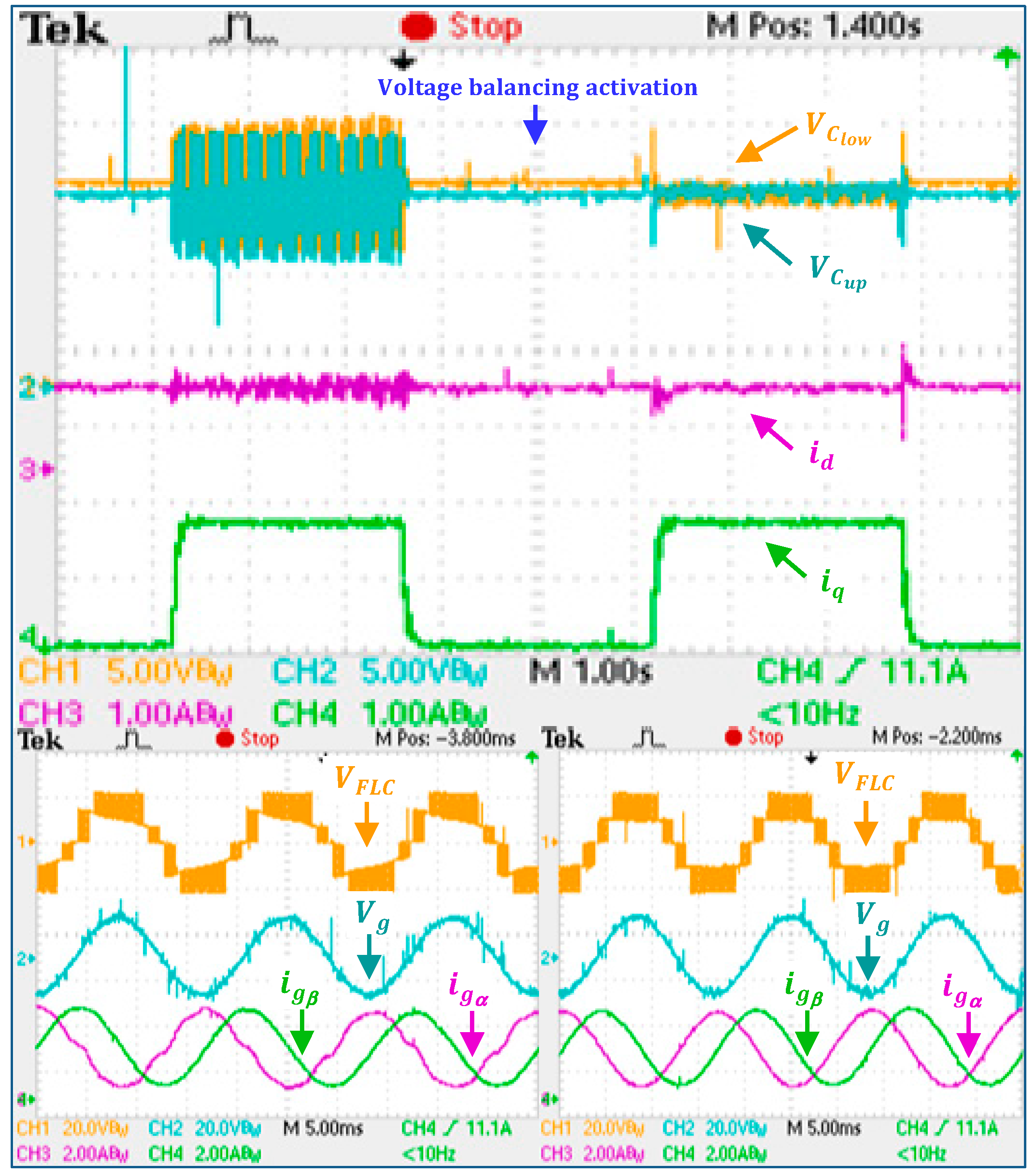
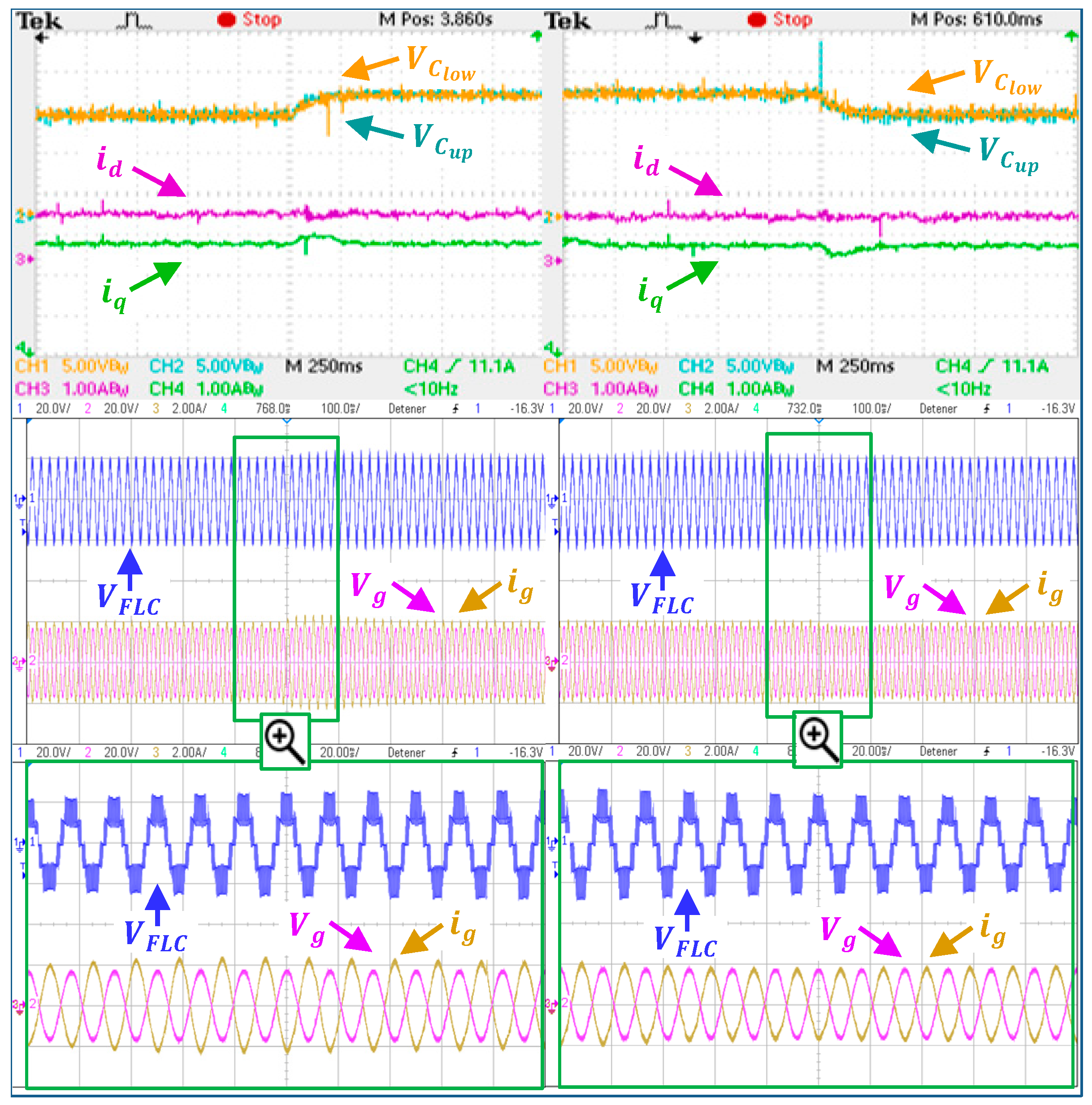
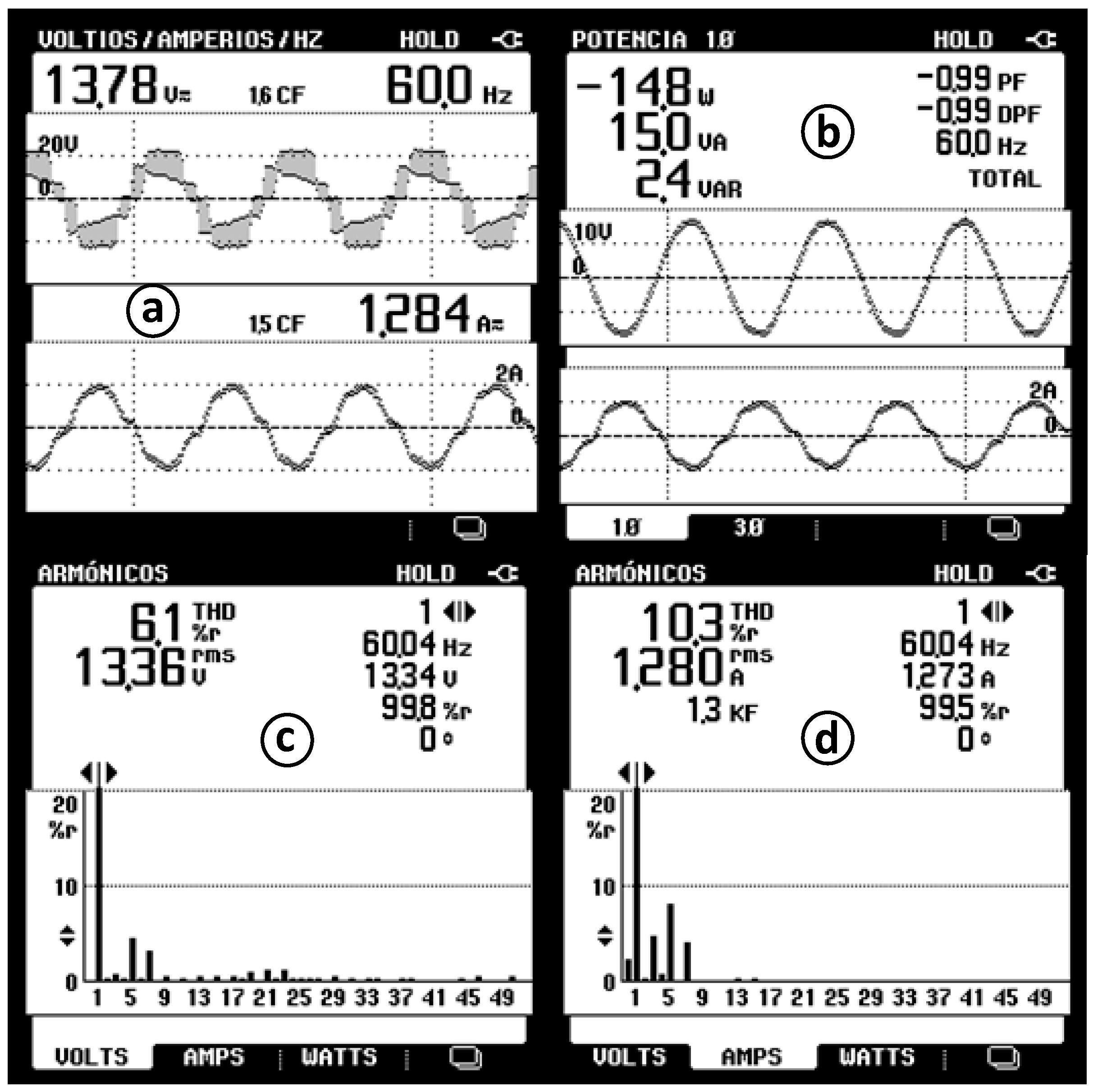
5. Experimental Results
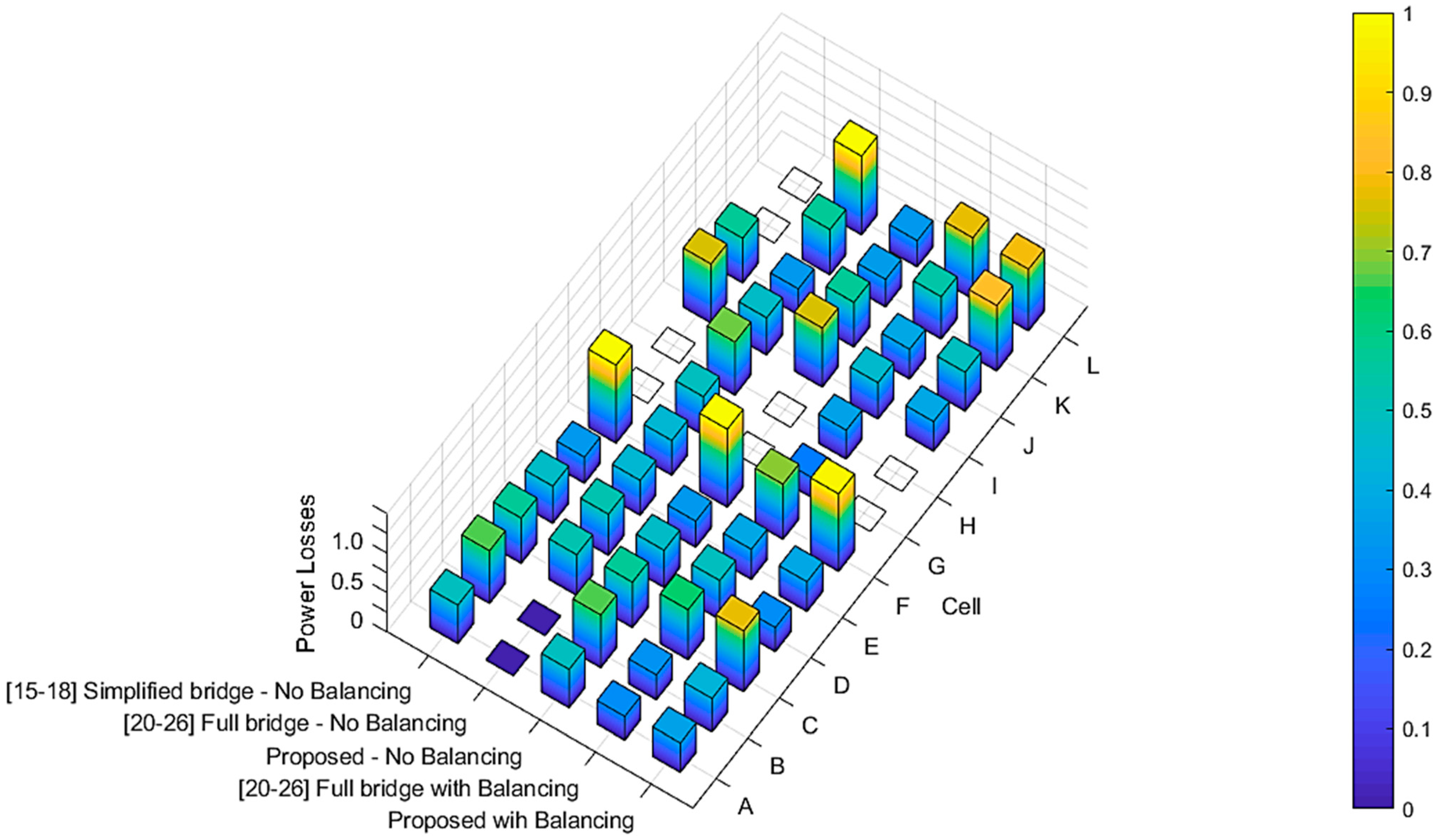
In order to validate the voltage balancing strategy, the current vector control technique and the proposed grid-tied SPFLC, they have been implemented and evaluated exhaustively. Figure 11 shows a photo of the experimental setup built in the laboratory, whereas its main parameters are summarized in Table 3.
The proposed five-level converter was built with MOSFETs power switches IRF640, drivers IR2110 and high-speed optocouplers 6N137. The floating sources have been obtained from isolated transformers followed by diode-bridge rectifiers. The voltage and current transducers used in the sensing stage are LV 25-P and CSLA2CD, respectively. The monitoring, processing and control tasks have been performed with the FPGA Spartan-3 and DSP F28335 boards.
The same tests performed in simulation for getting the results of Figure 6, Figure 7, Figure 8 and Figure 9 were also carried out experimentally. Figure 12, Figure 13, Figure 14 and Figure 15 show the main waveforms obtained from these tests, i.e., (a) steady state of the d q grid current components with i d * = 0 and i q * = 1.8 A; (b) a step-change in the q axis grid current from zero to 1.8 A and back to zero; (c) a grid voltage sag/swell from 15 Vpk to 12 Vpk (20%) and back to 15 Vpk (25%); and (d) a DC bus voltage step-change from 25 V to 30 V (20%) and back to 25 V (17%). It is remarkable to observe how from half the time scale, when the voltage balancing strategy is activated, the voltage unbalance of split capacitors notably reduces, the asymmetry of the SPFLC output voltage V F L C is properly corrected, the ripple of the direct current component i d decreases and the distortion of the grid current i g = i g α is fairly well-compensated while remaining accurately in quadrature with i g β ; thus, notably enhancing the power quality in the grid-tied SPFLC system. In general, it is noteworthy how the experimental results accurately match the ones from simulation, thus validating the good dynamic and steady-state performance of the proposed grid-tied SPFLC and its voltage balancing strategy. Bearing in mind that, in all of the tests, the reference of the direct grid current component i d * was set to zero and the electrical energy flowing direction was from the DC voltage source that feeds the bus of the SPFLC to the AC mains; hence, the grid current i g α = i g always remains out-of-phase with the grid voltage V g . The variables V C l o w , V C u p , V F L C , V g and i g shown in Figure 12, Figure 13, Figure 14 and Figure 15 have been directly measured from the grid-tied SPFLC prototype, whereas the variables i g α , i g β , i d and i q have been output in real-time from the vector control algorithm embedded within the DSP. For this, PWM pins and analog low-pass filters have been used. Given that the PWM outputs only deal with a positive polarity, their zero reference in the scopes was set as one square per division, i.e., 1 A and 2 A, respectively. All of the measurements were sensed through differential voltage probes and Hall current probes by simultaneously using the four channels of the TPS2024B Tektronix scope as well as the four channels of the MSOX3054A Agilent scope.
Figure 16 and Figure 17 show the experimental results obtained from the power quality analysis of the SPFLC output voltage V F L C and the grid current i g both without and with the activation of the DC-link split capacitors voltage balancing strategy. It is noteworthy that when the balancing algorithm is activated, the THD of V F L C and i g reduces from 6.1% and 10.3% to only 2.7% and 1.9%, respectively. Furthermore, the performance of the vector control for regulating the direct current component i d to zero alike enhances, thus maintaining i g more accurately out-of-phase with the grid voltage V g . Likewise, the balancing strategy also improves the power quality of the proposed grid-tied SPFLC, allowing it to achieve a unity power factor and a reactive power very close to zero, while the resulting grid current notably fulfills the standard IEEE 519 by maintaining its harmonic content far below the 5% limit.
With the aim of properly comparing the three different single-phase NPC five-level converters under study, the power loss distribution and the maximum power transfer efficiency are used as figures of merit.
Figure 18 shows the first figure of merit based on the power losses distribution for three different single-phase five-level NPC converters, both with and without the voltage balancing of the DC-link split capacitors. In order to perform a fair and straightforward comparison, the magnitude of the power losses was normalized by considering all the results at once. Likewise, for ease of analysis, the cells’ notation with the letters A–L in Figure 18 matches the description of the power devices within the topologies of Figure 1. The term cell denotes either the set of a switch with its antiparallel free-wheeling diode or a simple neutral clamping diode. Note that the cells G-H are only present in the full-bridge topology [20,21,22,23,24,25,26], whereas the cells K-L are only not present in the conventional simplified-bridge topology [15,16,17,18].
Table 4 shows the second figure of merit based on the maximum power transfer efficiency for three different five-level NPC converters, both with and without the voltage balancing of the DC-link split capacitors. It can be noted that the conventional simplified-bridge topology [15,16,17,18], having only six switches, is the most efficient, with 96.11%. Nevertheless, this configuration is inconveniently incapable of balancing the voltage of the split-capacitors. It is also noteworthy that the proposed topology is more efficient than the full-bridge topology [20,21,22,23,24,25,26] in both operation modes, i.e., with and without voltage balancing. Although this superiority in efficiency is quite small, the proposed topology also has the advantages of accounting for two less neutral clamping diodes and a voltage balancing strategy with a very low complexity.

6. Discussion

The experimental results shown in Section 5 properly validated the proposed SPFLC and its inherent DC-link voltage balancing strategy. Although the experimental setup is based on a low-power laboratory prototype, it can be seamlessly extended to a high-power system because the operating principle, theory and modeling behind the proposed topology and voltage balancing technique remain the same and are independent of the power level.
It is of significance to remark the different aspects that can affect the accuracy and validity of the experiments. The signal conditioning stage, built for interfacing the Hall-effect sensors that measure the voltage of the upper and lower split capacitors with the analog-to-digital converters of the DSP, is based on operational amplifiers and passive components such as resistors and capacitors. All the elements along this cascaded connection are inevitably prone to parameter variations due to temperature, thus affecting the gain and offset of the voltage measurements that are input to the control strategy for carrying out the voltage unbalancing compensation. Although the effect of an offset or a gain mismatch among the voltage sensors is only a constant DC unbalance bias, and even under these non-ideal conditions, the voltage ripple between the capacitors is completely compensated by the proposed balancing strategy, they have to be taken into account. Therefore, with the aim of guaranteeing the high accuracy and validity of the results, a digital calibration curve was implemented within the DSP. Furthermore, an automatic routine was also programmed for digitally removing the initial offset from the voltage sensors. To do this, before taking the initial voltage measurements, both of the split capacitors were discharged through a low-value resistor, and once the routine finished, the Hewlett Packard DC voltage source was connected to the terminals of the split capacitors.
The use of poor-quality measuring instruments as well as a weak grounding for the power system are other threats to the validity of experiments that can lead to biased and misleading results. However, in this work, a proper ground method was followed, which is in agreement with the literature. Moreover, accurate and high-performance instruments were used such as the power quality analyzer Fluke 43B, the scope Tektronix TPS2024B and the scope Agilent MSOX3054A.
The experimental results presented in Section 5 have been obtained at various times and in different days. Therefore, the repeatability of measurements as well as the good performance exhibited by the prototype under different conditions and scenarios can be interpreted as sufficient evidence for validating the setup. Bearing in mind that the experimental and simulation results presented throughout the paper agree, they thus mutually validate each other. Furthermore, the fact this study was properly compared to the already existing topologies in literature it gives us the reassurance that the obtained results are reliable.
On the other hand, it is also important to take notice that, even though the proposed topology is bidirectional, the voltage balancing strategy only applies for the inverter mode, i.e., when the energy flows from the DC source to the AC grid. Thus, the proposed topology is a good candidate for unidirectional applications such as photovoltaic, where the power always flows from the photovoltaic system to the grid or the load. Bearing in mind this situation, future research directions of the present work are the improvement of such five-level topology so that it becomes capable of balancing the voltage of split-capacitors in the rectifier mode too, i.e., when the energy flows from the AC grid to the DC side. The objective of future work on this matter is devising a multilevel NPC-converter with bidirectional voltage balancing capabilities, thereby expanding the fields and applications where it can be exploited.

7. Conclusions

A novel single-phase grid-tied neutral-point-clamped five-level converter with an inherent voltage balancing strategy that merges simplicity and effectivity was proposed and validated in this paper. The developed balancing strategy is based on a simple multicarrier phase disposition PWM modulation and only requires measuring the capacitors’ voltages and the sign of the converter output current for selecting the appropriate, compensating, switching vector from a LUT; thus, avoiding the complexity of conventional methodologies that modify the SVM or inject offset voltages into the CBPWM.
The obtained simulation and experimental results show a very good performance of the developed strategy for balancing the DC-link split capacitors in both steady state and transient conditions, e.g., a sudden variation in the q -axis grid current component, a grid voltage sag/swell and a DC bus voltage step-change. From the power quality analysis, it is noteworthy that the inherent balancing strategy of the implemented SPFLC makes possible obtaining straightforwardly a symmetrical five-level output voltage and a grid current with very low harmonic content, a more accurate vector control of the grid current and a better overall performance of the multilevel converter application.
A simple but effective voltage balancing strategy of the DC-link split capacitors, as the one presented in this paper, makes the proposed single-phase NPC five-level topology attractive and suitable for high-performance multilevel-based power applications such as the integration of photovoltaic energy to the grid, vehicle-to-grid V2G and standalone microgrids.

Author Contributions

All authors have equally contributed to the conceptualization, formal analysis, investigation, methodology, validation, and writing—review & editing of the paper. All authors have read and agreed to the published version of the manuscript.

Funding

This work was funded by the National Council of Science and Technology of Mexico (CONACYT) through its “Postdoctoral Fellowship Program” under grants 2019-000006-01NACV-00062 and 2020-000022-01NACV-00108.

Institutional Review Board Statement

Not Applicable.

Informed Consent Statement

Not Applicable.

Data Availability Statement

Not Applicable.

Acknowledgments

Authors would like to thank TNM Instituto Tecnológico de La Laguna for its partial support in this research.

Conflicts of Interest

Authors declare no conflict of interest.

Nomenclature

V d , V q direct and quadrature grid voltage components
i d , i q direct and quadrature grid current components
α β , d q stationary and rotating frames
X β , X ω variable in the stationary frame
X d , X q variable in the rotating frame
i g , V g grid current and grid voltage
f s , T s sampling frequency and sampling time
θ V g , θ i g phase of grid voltage and phase of grid current
ω g angular frequency of grid
V d c DC bus voltage of FLC
f s w , T s w switching frequency and switching period
t , T continuous time and fundamental period
Ttranspose matrix
P , P 1 direct and inverse Park matrices
k p , k i proportional and integral gains of PI controllers

References

  1. Kuncham, S.K.; Annamalai, K.; Subrahmanyam, N. A two-stage T-type hybrid five-level transformerless inverter for PV applications. IEEE Trans. Power Electron. 2020, 35, 9510–9521. [Google Scholar] [CrossRef]
  2. Gautam, S.P.; Kumar, L.; Gupta, S.; Agrawal, N. A single-phase five-level inverter topology with switch fault-tolerance ca-pabilities. IEEE Trans. Power Electron. 2017, 64, 2004–2014. [Google Scholar]
  3. Monteiro, V.; Ferreira, J.C.; Melendez, A.A.N.; Afonso, J.L. Model predictive control applied to an improved five-level bidirectional converter. IEEE Trans. Ind. Electron. 2016, 63, 5879–5890. [Google Scholar] [CrossRef]
  4. Kang, K.-P.; Cho, Y.; Ryu, M.-H.; Baek, J.-W. A harmonic voltage injection based DC-link imbalance compensation technique for single-phase three-level neutral-point-clamped (NPC) inverters. Energies 2018, 11, 1886. [Google Scholar] [CrossRef] [Green Version]
  5. Jun, E.-S.; Kwak, S. A Highly efficient single-phase three-level neutral point clamped (NPC) converter based on predictive control with reduced number of commutations. Energies 2018, 11, 3524. [Google Scholar] [CrossRef] [Green Version]
  6. Jun, E.-S.; Nguyen, M.H.; Kwak, S. Model predictive control method based on deterministic reference voltage for single-phase three-level NPC converters. Appl. Sci. 2020, 10, 8840. [Google Scholar] [CrossRef]
  7. Zanasi, R.; Tebaldi, D. Modeling control and robustness assessment of multilevel flying-capacitor converters. Energies 2021, 14, 1903. [Google Scholar] [CrossRef]
  8. Kim, J.-M.; Song, G.-S.; Jung, J.-J. Zero-sequence voltage injection method for DC capacitor voltage balancing of wye-connected CHB converter under unbalanced grid and load conditions. Energies 2021, 14, 1019. [Google Scholar] [CrossRef]
  9. Saeedian, M.; Hosseini, S.M.; Adabi, J. A five-level step-up module for multilevel inverters: Topology, modulation strategy, and implementation. IEEE J. Emerg. Sel. Top. Power Electron. 2018, 6, 2215–2226. [Google Scholar] [CrossRef]
  10. Buticchi, G.; Lorenzani, E.; Franceschini, G. A five-level single-phase grid-connected converter for renewable distributed sys-tems. IEEE Trans. Power Electron. 2013, 60, 906–918. [Google Scholar]
  11. He, X.; Lin, X.; Peng, X.; Han, P.; Shu, Z.; Gao, S. Control strategy of single-phase three level neutral point clamped cascaded rectifier. Energies 2017, 10, 592. [Google Scholar]
  12. Peng, X.; He, X.; Han, P.; Guo, A.; Shu, Z.; Gao, S. Smooth switching technique for voltage balance management based on three-level neutral point clamped cascaded rectifier. Energies 2016, 9, 803. [Google Scholar] [CrossRef]
  13. Khan, S.A.; Islam, M.R.; Guo, Y.; Zhu, J. An amorphous alloy magnetic-bus-based SiC NPC converter with inherent voltage balancing for grid-connected renewable energy systems. IEEE Trans. Appl. Supercond. 2019, 29. [Google Scholar] [CrossRef]
  14. Rao, A.M.; Sivakumar, K. A Fault-tolerant single-phase five-level inverter for grid-independent PV systems. IEEE Trans. Ind. Electron. 2015, 62, 7569–7577. [Google Scholar] [CrossRef]
  15. Haddad, M.; Rahmani, S.; Hamadi, A.; Al-Haddad, K. New Single Phase Multilevel Reduced Count Devices to Perform Active Power Filter. In Proceedings of the Institute of Electrical and Electronics Engineers (IEEE), Fort Lauderdale, FL, USA, 9–12 April 2015; pp. 1–6. [Google Scholar]
  16. Javadi, A.; Abarzadeh, M.; Gregoire, L.-A.; Al-Haddad, K. Real-time HIL implementation of a single-phase distribution level THSeAF based on D-NPC converter using proportional-resonant controller for power quality platform. IEEE Access 2019, 7, 110372–110386. [Google Scholar] [CrossRef]
  17. Javadi, A.; Hamadi, A.; Ndtoungou, A.; Al-Haddad, K. Power quality enhancement of smart households using a multi-level-THSeAF with a PR controller. IEEE Trans. Smart Grid 2017, 8, 465–474. [Google Scholar] [CrossRef]
  18. Hamadi, A.; Rahmani, S.; Al-Haddad, K.; Addoweesh, K.; Hamadi, A. Micro Grid Based PMSG Feeding Isolated Loads. In Proceedings of the 2014 IEEE Applied Power Electronics Conference and Exposition—APEC 2014, Fort Worth, TX, USA, 16–20 March 2014; pp. 3160–3165. [Google Scholar]
  19. Zhou, T.; Shu, Z.; Lin, H.; Luo, D.; Chen, Y.; Guo, X. A high-power-density single-phase rectifier based on three-level neutral-point clamped circuits. Energies 2017, 10, 697. [Google Scholar] [CrossRef] [Green Version]
  20. Stala, R. Application of balancing circuit for DC-link voltages balance in a single-phase diode-clamped inverter with two three-level legs. IEEE Trans. Ind. Electron. 2010, 58, 4185–4195. [Google Scholar] [CrossRef]
  21. Song, W.; Feng, X.; Smedley, K.M. A carrier-based PWM strategy with the offset voltage injection for single-phase three-level neutral-point-clamped converters. IEEE Trans. Power Electron. 2013, 28, 1083–1095. [Google Scholar] [CrossRef]
  22. Wensheng, S.; Shunliang, W.; Chenglin, X.; Xinglai, G.; Xiaoyun, F. Single-phase three-level space vector pulse width modu-lation algorithm for grid-side railway traction converter and its relationship of carrier-based pulse width modulation. IET Electr. Syst. Transp. 2014, 4, 78–87. [Google Scholar]
  23. Wang, S.; Ma, J.; Liu, B.; Jiao, N.; Liu, T.; Wang, Y. Unified SVPWM algorithm and optimization for single-phase three-level npc converters. IEEE Trans. Power Electron. 2020, 35, 7702–7712. [Google Scholar] [CrossRef]
  24. Salaet, J.; Gilabert, A.; Bordonau, J.; Alepuz, S.; Cano, A.; Gimeno, L.M. Nonlinear control of neutral point in three-level single-phase converter by means of switching redundant states. IEE Electron. Lett. 2006, 42, 304–306. [Google Scholar] [CrossRef]
  25. Sanchez-Ruiz, A.; Abad, G.; Echeverria, I.; Torre, I.; Atutxa, I. Continuous phase-shifted selective harmonic elimination and DC-link voltage balance solution for h-bridge multilevel configurations, applied to 5L HNPC. IEEE Trans. Power Electron. 2016, 32, 2533–2545. [Google Scholar] [CrossRef]
  26. Lee, J.-S.; Kwak, R.; Lee, K.-B. Novel discontinuous PWM method for a single-phase three-level neutral point clamped inverter with efficiency improvement and harmonic reduction. IEEE Trans. Power Electron. 2018, 33, 9253–9266. [Google Scholar] [CrossRef]
  27. Calais, M.; Borle, L.J.; Agelidis, V.G. Analysis of Multicarrier PWM Methods for a Single-phase Five Level Inverter. In Proceedings of the 2001 IEEE 32nd Annual Power Electronics Specialists Conference (IEEE Cat. No.01CH37230), Vancouver, BC, Canada, 17–21 June 2001; pp. 1351–1356. [Google Scholar]
  28. Arab, N.; Vahedi, H.; Al-Haddad, K. LQR control of single-phase grid-tied PUC5 inverter with LCL filter. IEEE Trans. Ind. Electron. 2020, 67, 297–307. [Google Scholar] [CrossRef]
  29. Bahrani, B.; Rufer, A.; Kenzelmann, S.; Lopes, L.A.C. Vector control of single-phase voltage-source converters based on fictive-axis emulation. IEEE Trans. Ind. Appl. 2011, 47, 831–840. [Google Scholar] [CrossRef]
  30. Ziarani, A.; Konrad, A.; Sinclair, A. A novel time-domain method of analysis of pulsed sine wave signals. IEEE Trans. Instrum. Meas. 2003, 52, 809–814. [Google Scholar] [CrossRef]
Figure 1. Single-phase NPC five-level converters; (a) conventional simplified-bridge topology [15,16,17,18], (b) full-bridge topology [20,21,22,23,24,25,26], and (c) proposed topology.
Energies 14 02644 g001
Figure 2. Current flowing paths for the seven switching states of the proposed SPFLC; (a) proposed topology; (b) State 1 [ + V d c ] ; (c) State 2 U [ + V d c / 2 ] from upper capacitor; (d) State 2 L [ + V d c / 2 ] from lower capacitor, (e) state 3 [ 0 ] ; (f) state 4 U [ V d c / 2 ] from upper capacitor; (g) state 4 L [ V d c / 2 ] from lower capacitor; and (h) state 5 [ V d c ] .
Energies 14 02644 g002
Figure 3. MPDPWM modulation strategy: reference and carrier signals, switching pattern and the resulting output voltage from the proposed SPFLC.
Energies 14 02644 g003
Figure 4. Block diagram of the proposed grid-tied SPFLC and its current vector control in the d q rotating coordinates.
Energies 14 02644 g004
Figure 5. Space vector diagram of the stationary a b c / α β reference frames and the rotating d q coordinates.
Energies 14 02644 g005
Figure 6. Performance of the voltage balancing strategy and the vector control for the proposed grid-tied SPFLC during steady state of the d q grid currents.
Energies 14 02644 g006
Figure 7. Performance of the voltage balancing strategy and the vector control for the proposed grid-tied SPFLC during a step-change in the q axis grid current.
Energies 14 02644 g007
Figure 8. Performance of the voltage balancing strategy and the vector control for the proposed grid-tied SPFLC during a grid voltage sag/swell.
Energies 14 02644 g008
Figure 9. Performance of the voltage balancing strategy and the vector control for the proposed grid-tied SPFLC during a DC bus voltage step-change.
Energies 14 02644 g009
Figure 10. Dynamic response of the voltage balancing strategy and the vector control for the proposed grid-tied SPFLC during a sweep of the capacitance of the DC-link split capacitors.
Energies 14 02644 g010
Figure 11. Experimental setup built in the laboratory; (a) novel single-phase five-level converter and its drivers; (b) auxiliary DC voltage sources; (c) grid connectors board; (d) line inductor; (e) Tektronix Hall current probes; (f) grid variable autotransformer; (g) multimeters; (h) voltage/current Hall sensors and signal conditioning stage; (i) DSP/FPGA-based control cards; (j) control dashboard; (k) Hewlett Packard programmable DC voltage source; (m) PC—Windows 10/i7/8 Gb RAM; and (n) Tektronix/Agilent digital scopes and Fluke 43B.
Energies 14 02644 g011
Figure 12. Performance of the voltage balancing strategy and the vector control for the proposed grid-tied SPFLC during steady state of the d q grid currents.
Energies 14 02644 g012
Figure 13. Performance of the voltage balancing strategy and the vector control for the proposed grid-tied SPFLC during a step-change in the q axis grid current.
Energies 14 02644 g013
Figure 14. Performance of the voltage balancing strategy and the vector control for the proposed grid-tied SPFLC during a grid voltage sag/swell.
Energies 14 02644 g014
Figure 15. Performance of the voltage balancing strategy and the vector control for the proposed grid-tied SPFLC during a DC bus voltage step-change.
Energies 14 02644 g015
Figure 16. Fluke 43B-based power quality analysis of grid-tied SPFLC waveforms without the activation of the DC-link split capacitors’ voltage balancing. (a) SPFLC output voltage V F L C and the resulting grid current i g from the vector control technique; (b) grid powers, grid factors, V g and i g ; (c) spectrum of V F L C ; and (d) spectrum of i g .
Energies 14 02644 g016
Figure 17. Fluke 43B-based power quality analysis of grid-tied SPFLC waveforms with the activation of the DC-link split capacitors’ voltage balancing. (a) SPFLC output voltage V F L C and the resulting grid current i g from the vector control technique; (b) grid powers, grid factors, V g and i g ; (c) spectrum of V F L C ; and (d) spectrum of i g .
Energies 14 02644 g017
Figure 18. Figure of merit based on the power loss distribution for different five-level NPC converters with and without the voltage balancing of the DC-link split capacitors.
Energies 14 02644 g018
Table 1. Comparison of five-level NPC converters.
FeatureNumber Of ComponentsVoltage Balancing
Fl Npc TopologyCapacitorsSwitchesDiodesTotalCapabilityComplexity
Simplified-Bridge (SB)
[15,16,17,18]
2628NO-
Full-Bridge (FB)
[20,21,22,23,24,25,26]
28412YESHIGH
Proposed28210YESLOW
Table 2. Switching states and voltage balancing strategy for the proposed five-level converter.
Switching StateState of SwitchesFlc Output
Voltage
( V F L C )
Voltage
Balancing
Algorithm
Activated
Capacitors Unbalance Voltage
(ΔV)
Flc Output Current Sign
( i F L C )
S 1 S 3 S 5 S 7 S 2 S 4 S 6 S 8
101111001 + V d c
2U01111000 + V d c /2YES + +
2L00111101NO/YESOTHERWISE
3000111110
4U10110101 V d c /2NO/YESOTHERWISE
4L10000111YES
510010111 V d c
Table 3. Parameters of simulation and experimental grid-tied SPFLC.
ParameterSymbolValueUnits
SimulationExperimental
Switching frequency f s w 55kHz
Line resistance R L 0.10.1Ω
Line inductance L L 53mH
Grid voltage (peak) V g 18015V
Grid frequency f 6060Hz
DC bus voltage V d c 25025V
Capacitance of split capacitors C u p , C l o w 200300μF
Sampling time/Time-step T s 100100μs
Table 4. Figure of merit based on the efficiency of different five-level NPC converters with and without the voltage balancing of the DC-link split capacitors.
Five-Level
Npc Converter
Efficiency (%)
Without Voltage BalancingWith Voltage Balancing
Simplified-bridge [15,16,17,18]96.11-
Full-bridge [20,21,22,23,24,25,26]95.2695.13
Proposed95.5595.37
Publisher’s Note: MDPI stays neutral with regard to jurisdictional claims in published maps and institutional affiliations.

