Article

A New Soft-Switching Solution in Three-Level Neutral-Point-Clamped Voltage Source Inverters

Department of Electrical Engineering, Cracow University of Technology, 31-155 Krakow, Poland
*
Author to whom correspondence should be addressed.
Energies 2021, 14(8), 2247; https://doi.org/10.3390/en14082247
Submission received: 25 February 2021 / Revised: 29 March 2021 / Accepted: 13 April 2021 / Published: 16 April 2021
(This article belongs to the Section F: Electrical Engineering)

Abstract

:
This paper presents a new soft-switching solution recommended for three-level neutral-point-clamped inverters. The operation principles of the proposed solution, working stages, selection of elements, and the control algorithm are comprehensively discussed herein. The control method of the inverter main switches is the same as that of the switches of an inverter operating according to the hard-switching technique. The correctness of the proposed solution was confirmed by the results of different tests using a laboratory neutral-point-clamped inverter with rated parameters of 3 kW, 2 × 150 V, 12 A, and 3 kHz. Numerical analyses were performed for the inverter of rated power 1.2 MW. The switching losses of the inverter operating with the proposed solution were compared with those of an inverter with hard-switching method. The proposed soft-switching solution increased the inverter efficiency and its competitiveness in relation to other proposals because there were no connections between switches and capacitors or inductors, which pose a risk of damaging the inverter when disturbances in the control system appear.

1. Introduction

Three-phase three-level neutral-point-clamped (3LNPC) inverters are usually employed in industrial and traction drive systems with medium and high-power induction motors. These inverters are also applied in systems for the conversion and transmission of electrical energy, and increasingly often in generation systems from renewable sources. Insulated gate bipolar transistors (IGBTs), gate turn-off thyristors (GTOs), and integrated gate commutated thyristors (IGCTs) are mainly used as semiconductor switches. It is understandable that the switching frequency decreases with increases in the rated power of voltage source inverters (VSIs). The 3LNPC inverters have more favourable possibilities of output voltage shaping with respect to two-level inverters, because a significant reduction in higher harmonics in the load currents can be obtained at lower switching frequencies in comparison to two-level inverters.
The efficiency of three-level inverters depends primarily on both conduction and switching losses [1,2,3]. The first type of losses depends on both the switch conduction current and the voltage drop across the switch. The efficiency is significantly influenced by losses in diodes, especially by the losses occurring during the reverse-recovery processes. The switching losses can be significantly reduced using different soft-switching systems, by which switches are turned ON and turned OFF when their currents or voltages are almost equal to zero. In some cases, the same two soft-switching circuits, having relatively small additional elements, support switching processes in all inverter phases [4,5,6]. However, control algorithms of these systems are usually complex, and the frequency of the inverter output voltage can change in a narrow range.
The second group of soft-switching systems includes solutions that support the switching processes individually in each phase of the given three-level inverter [7,8,9,10,11,12]. An advantage of these solutions is the ability to support switching processes in a wide range of output frequencies, especially when the inverter should operate with different methods of pulse width modulation.
Typically, soft-switching solutions have additional circuits containing, among others, capacitors connected to main switches [7,10,13,14,15,16]. In the case of disturbances, one of the main switches may be turned ON at a non-zero voltage of the capacitor which is connected in parallel with this switch; as a result, the switch current may reach an unacceptable value. In other existing solutions of soft-switching, transistors or the above-mentioned thyristors are connected in series with additional inductors or with inductive loads [4,10,11,14]. When a given switch is turned OFF at a non-zero current of the inductor, then an overvoltage appears, which is usually dangerous to this switch. Soft-switching systems that do not have those connections of capacitors and inductors were also proposed [9], but their control algorithm is notably complex because the start of the switching process of any main switch has to be preceded by the turn-ON of the appropriate auxiliary switch at a specific moment. However, this operation principle is quite inconvenient when, for example, an inverter operates with pulse width modulation or an induction motor must be controlled by a space-vector modulation method.
The aim of this article is to present a new soft-switching solution in 3LNPC inverters, competitive with the existing systems of this type. Unlike these systems, in the proposed solution capacitors are not connected in parallel to the main switches, and inductors are not connected in series with auxiliary switches. This leads to an improvement in the operational reliability of inverters with soft-switching systems. The authors propose a simple control algorithm of auxiliary switches, which are turned ON and turned OFF depending on operating states of the main switches, not the other way around. Loss calculations performed for a 3LNPC inverter with a rated power of 1.2 MW show a significant increase in efficiency.

2. Proposed Soft-Switching System in Three-Level Neutral-Point-Clamped Inverter

2.1. Structure and Operation Principles

It was assumed that IGBTs were applied as full-controlled switches in three-phase 3LNPC inverters. The structure of the proposed system is shown in Figure 1; this system is slightly modified with respect to the original system presented in [17,18,19]. Both voltage sources, marked in Figure 1 as UDC1 and UDC2, set the same voltage UDC. Capacitors C11–C14 are applied to decrease the steepness of the voltage increase in the main switches S11–S14 during their turn-OFF processes. The use of inductors L11–L14 is intended to reduce the rate of the current rise of these switches during their turn-ON processes. It was assumed that switches S13 and S14 and corresponding switches S13a and S14a are not turned ON when the current flows to the terminal A of the load; for the opposite load current direction, switches S11, S12, S11a, and S12a are not turned ON. The system operation analysis was performed for two cases; in the first case, S11 was switched ON/OFF, and S12 was still turned ON; in the second case, S11 was still turned OFF and S12 was switched ON/OFF. The operation principles are described for one switching cycle, assuming that the load current IL had a constant value in the analysed stages.

2.2. Working Stages—Switch S11

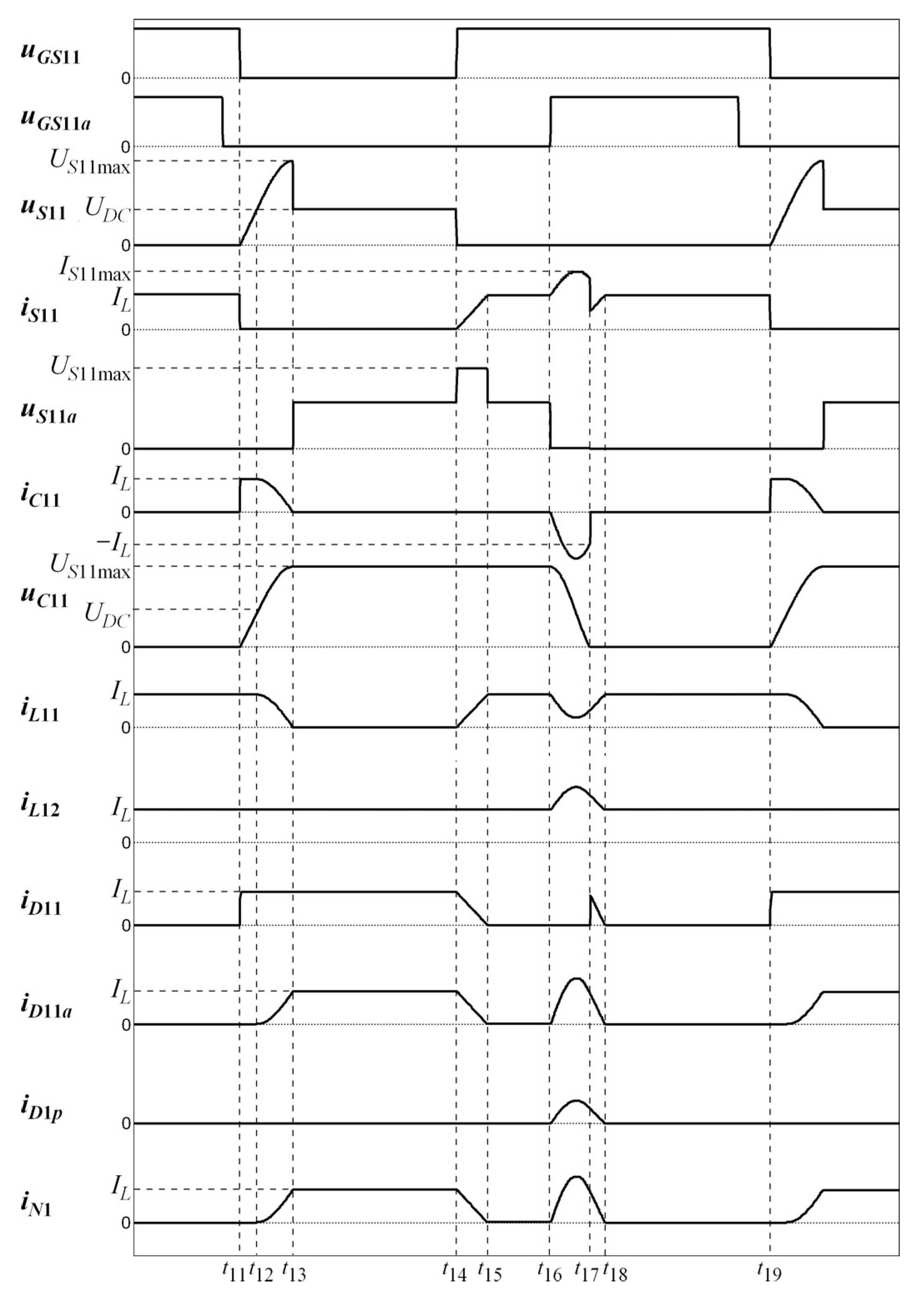
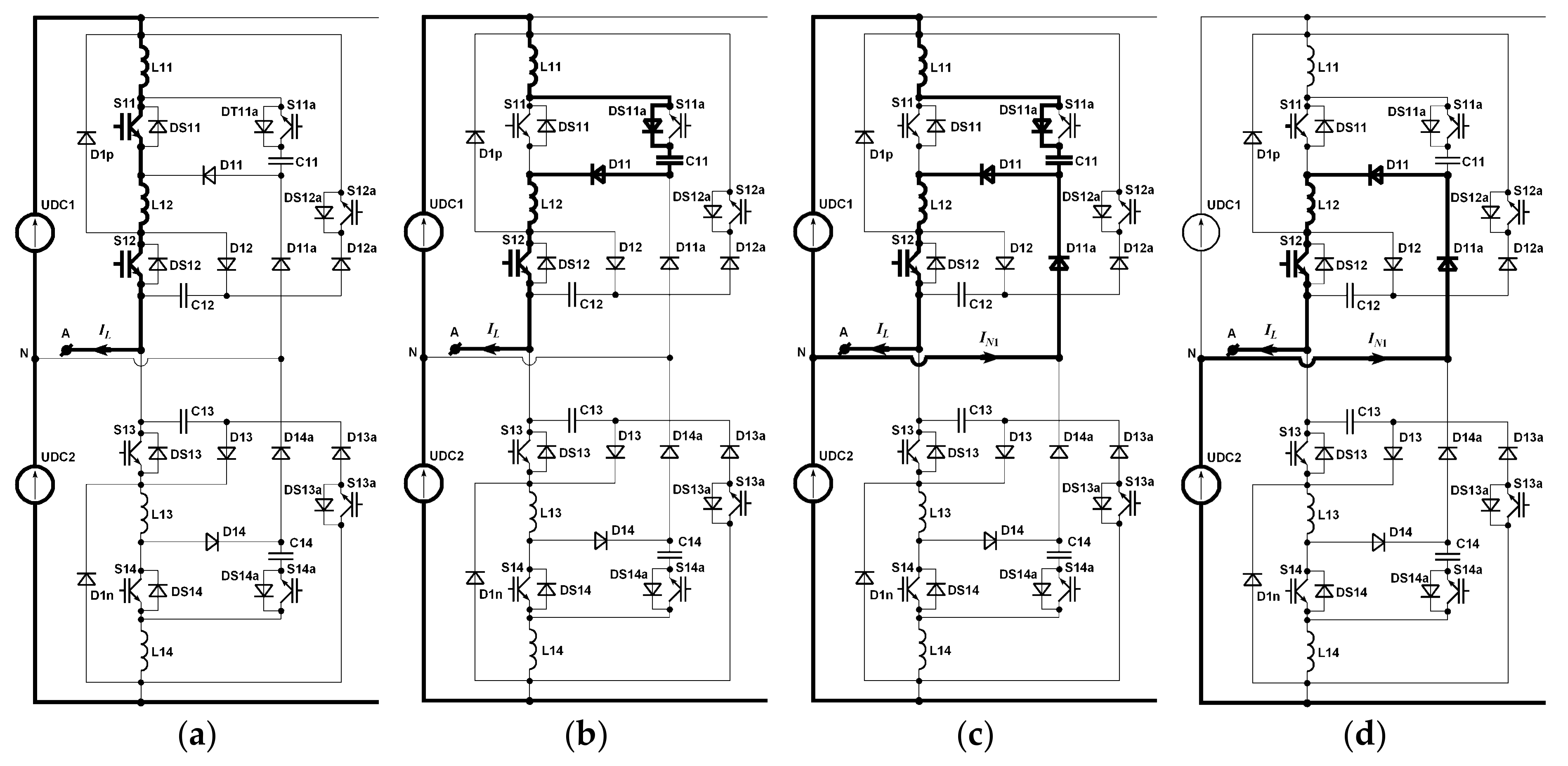
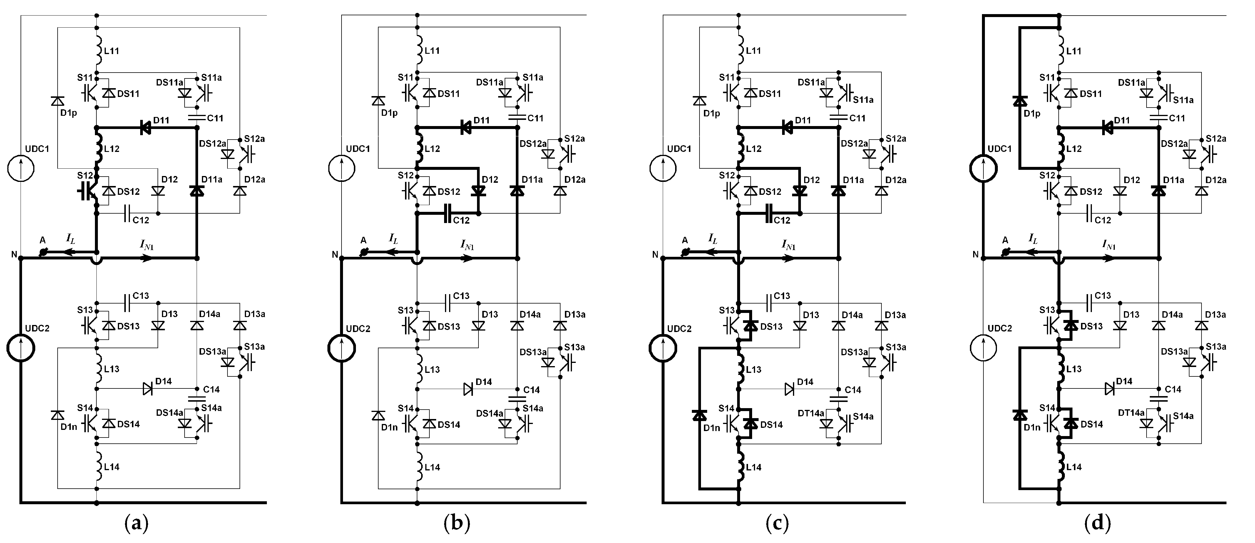
In this stage, switch S12 is in conduction state, and S11 is switched ON/OFF; the current of switch S12 is equal to the load current ILA, hereinafter referred to as IL. Simplified waveforms of chosen currents and voltages are shown in Figure 2. Before the beginning of the discussed cycle, the control signal of the switch S11 has a high value. This means that this switch is in a conduction state; other switches are in non-conduction states. The load current IL flows through switch S11, and the voltage of capacitor C11 is equal to zero. The load current IL flows from voltage source UDC1 through inductor L11, first main switch S11, inductor L12, and through the second main switch S12 to the load phase A (Figure 3a).

2.2.1. Stage t11t12

Switch S11 is turned OFF at time t11 (Figure 3b). From this moment, the load current IL flows through capacitor C11, and its voltage increases linearly with time; the voltage of switch S11 changes similarly. This allows us to conclude that the turn-OFF process of the switch S11 is soft. The current IL flows through inductor L11, diode DS11a, capacitor C11, diode D11, inductor L12, and switch S12.
Assuming that n relates to a certain switching cycle, the voltage of this capacitor and the voltage of switch S11 change their values as follows:
u S 11 ( t ) = u C 11 ( t ) = I L ( n ) C 11   t ,
where uC11(t11) = 0.
At time t12, the voltage of capacitor C11 reaches voltage UDC and this operating stage ends.

2.2.2. Stage t12t13

As shown in Figure 3c, from time t12, the load current IL flowing through diode D11, inductor L12, and switch S12 is the sum of two currents; the first one flows through diode D11a from the voltage source UDC2 (point N), and the second current flows through inductor L11 and diode DS11a. In this stage, capacitor C11 is resonantly charged to a voltage higher than UDC.
Changes in the capacitor voltage can be described as follows:
C 11 L 11 d 2 u C 11 ( t ) d t 2   + u C 11 ( t ) = U D C 1 ,
where uC11(t12) = UDC1, and iL11(t12) = IL(n).
Assuming that UDC1 = UDC2 = UDC, the next formulas enable determination of the capacitor voltage and current:
u C 11 ( t ) = U D C + L 11 C 11 I L ( n ) sin t C 11 L 11 ,
i C 11 ( t ) = I L ( n ) cos t C 11 L 11 .
The maximum capacitor voltage is determined as follows:
U C 11 max ( n ) = U D C + L 11 C 11 I L ( n ) .
Notably, in the time interval t11t13, the voltage of main switch S11 changes as the voltage of capacitor C11 changes.

2.2.3. Stage t13t14

As shown in Figure 3d, from time t13, the load current IL flows only from voltage source UDC2 through diodes D11a, D11, inductor L12, and switch S12 to terminal A of the load. The voltage of switch S11 decreases rapidly to voltage UDC; the voltages of other elements do not change.

2.2.4. Stage t14t15

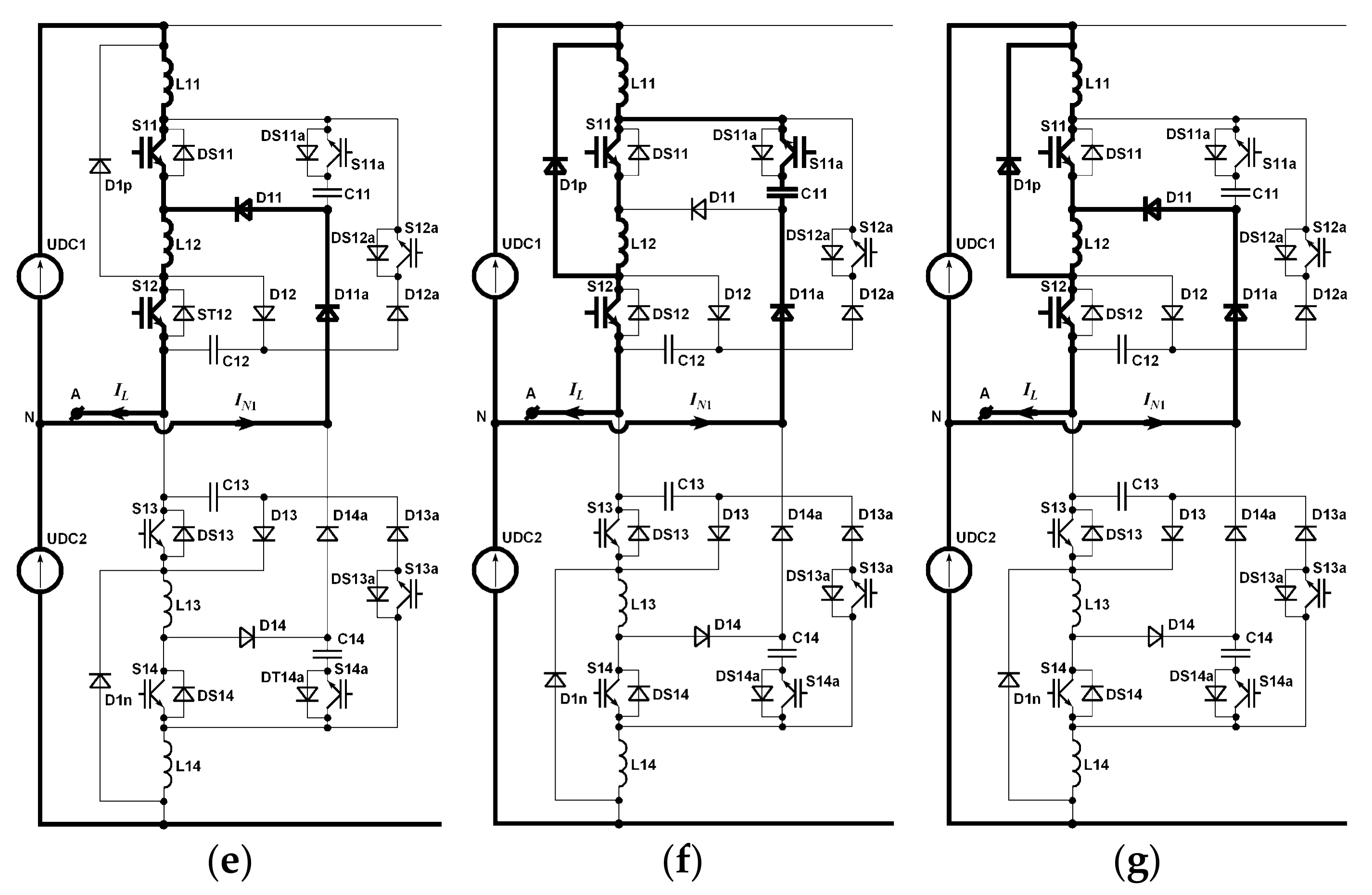
Switch S11 is turned ON at time t14 (Figure 3e). The current of switch S11 increases slowly to the load current IL. This current, which is equal to the current of inductor L11, is described by the following equation:
L 11 d i L 11 d t = U D C ,
where iL11(t14) = 0.
In this stage, the current changes of main switch S11 are described as follows:
i S 11 ( t ) = i L 11 ( t ) = U D C L 11 t .
Main switch S11 is turned ON at a current close to zero. Therefore, this turn-ON process can be treated as a soft-switching process. At time t15, the current of switch S11 reaches the value IL. The current flows similarly as in the initial state (Figure 3a). The voltage of capacitor C11 has the highest value in the considered cycle.

2.2.5. Stage t15t16

The time period t15t16 is not constant and it depends on the current IL. The resonant discharge process of the capacitor C11 can start when the current of the switch S11 rises to the load current. The longest increase in current S11 occurs if the load current is at its maximum, then the time interval t15t16 is equal to zero. Due to a simplification of the control algorithm, it was assumed that the turn-ON signal of the switch S11a does not depend on the instantaneous value of the load current IL, and this signal is generated with the same time delay in relation to the turn-ON signal of switch S11 in each switching cycle.

2.2.6. Stage t16t17

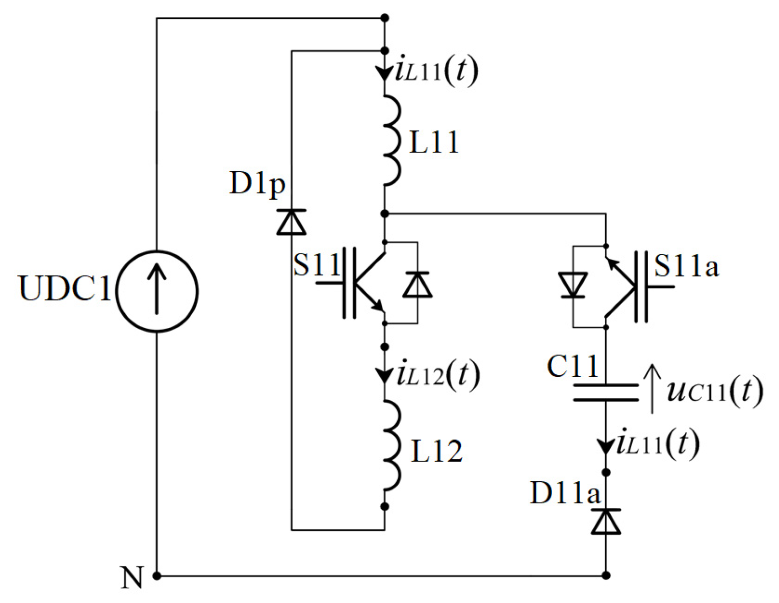
As shown in Figure 3f, at time t16, auxiliary switch S11a is turned ON, and from this moment capacitor C11 partly discharges resonantly through S11a, L11, UDC1, and D11a and partly through S11a, S11, L12, D1p, UDC1, and D11a (Figure 4).
The following equation system allows determining both the capacitor voltage and current:
L 11 d i L 11 ( t ) d t + u C 11 ( t ) = U D C 1 L 11 d i L 11 ( t ) d t + L 12 d i L 12 ( t ) d t = 0 i L 11 ( t ) i C 11 ( t ) i L 12 ( t ) = 0 ,
where iL11(t16) = iL12(t16) = IL, uC11(t16) = US11max.
Solving this system of equations, the resulting formulas describing the capacitor voltage and current are as follows:
u C 11 ( t ) = U D C + ( k 1 ) U D C cos ( ω 11 t ) + I L ( n ) L e q C 11 sin ( ω 11 t )   ,
i C 11 ( t ) = ( k 1 ) U D C C 11 L e q sin ( ω 11 t ) + I L ( n ) cos ( ω 11 t ) ,
where k = U C 11 max U D C in the considered cycle, and ω 11 = 1 L e q C 11 ,   L e q = L 11 L 12 L 11 + L 12 .
Notably, in this case the direction of the capacitor discharge current is marked in the opposite way with respect to those in Figure 1 and Figure 4.
To calculate the maximum current of switch S11a, the time tmax at which the derivative of the current iC11(t) equals zero must be determined. This time is expressed as follows:
t max = arctg ( k 1 ) C 11 L e q U d I L ( n ) + π ω 11 .
Hence, the maximum current values of switches S11 and S11a are as follows, respectively:
I S 11 a max = ( k max 1 ) U D C C 11 L e q sin ( ω 11 t max ) + I L ( n ) cos ( ω 11 t max )   ,
I S 11 max = I L max + I S 11 a max L 11 L 11 + L 12 ,
where ILmax denotes the maximum load current.
The energy of the electric field of capacitor C11 is delivered to voltage source UDC1, and at time t17 this process ends. Owing to the resonant nature of the discharging current, switch S11a is turned OFF softly. Auxiliary switch S11a can be turned OFF when capacitor C11 is fully discharged.

2.2.7. Stage t17t18

At time t17, capacitor C11 is completely discharged (Figure 3g). From this time, the currents of inductors L11 and L12 vary linearly with time and reach the load current IL at time t18; the current of the second inductor flows partially through diodes D1p, voltage source UDC1, and diodes D11a and D11. This time interval occurs only if k > 2. This state lasts until the moment at which switch S11 is turned OFF again. At time t19, the main switch S11 is turned OFF again.
The capacitances and inductances are determined for the inverter rated load, as described in Section 3. Then, the switching losses are significantly reduced. When the load current is significantly smaller with respect to the rated current, the operation character of the soft-switching system changes slightly. Main switch S11 is turned OFF (t11 in Figure 2); therefore, capacitor C11 is charged with a lower load current, and the capacitor voltage reaches a maximum value lower than twice UDC in the individual operation cycles. As a result, the discharge of the capacitor after turn-ON of the auxiliary switch S11a is not complete. Thus, the next turn-OFF process of switch S11 does not occur at zero voltage, and this process is partially “hard”. This results in a reduction in the efficiency of the discussed inverter. A similar situation occurs when switch S12 is turned ON and OFF.

2.3. Working Stages—Switch S12

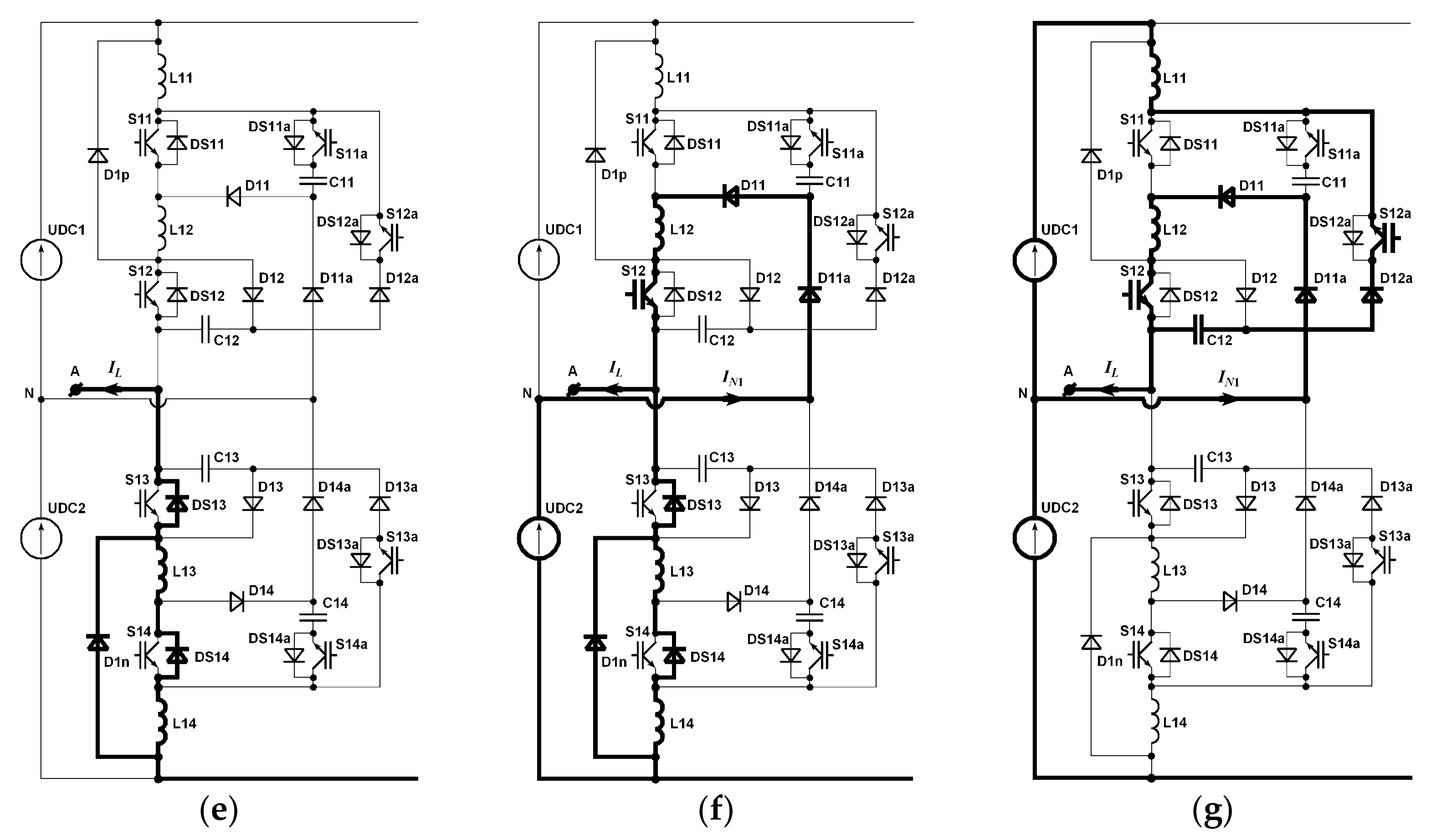
In this case, switch S11 is in non-conduction state, and S12 is switched ON/OFF. Figure 5 shows the simplified waveforms of chosen currents and voltages. The load current IL flows through switch S12 at the beginning of the discussed cycle. The voltage of capacitor C12 is equal to zero. The load current IL flows from voltage source UDC2 through D11a, D11, L12, and S12 to the load phase A (Figure 6a).

2.3.1. Stage t21t22

Switch S12 is turned OFF at time t21 (Figure 6b). The voltage of switch S12 is close to zero during the turn-OFF process owing to the charging of capacitor C12. Thus, it allows us to conclude that this switch is turned OFF softly. A constant current IL flows from source UDC2 to the load phase A through diodes D11a, D11, inductor L12, diode D12, and capacitor C12, causing it to charge:
u S 12 ( t ) = u C 12 ( t ) = I L ( n ) C 12   t ,
where uC12(t21) = 0. This stage lasts until the moment at which the capacitor voltage reaches the value UDC. The load current IL(n) influences the duration of this process.

2.3.2. Stage t22t23

The voltage of capacitor C12 reaches the value UDC at time t22 (Figure 6c). After this moment, the load current IL flows partly from UDC2 (point N) through diodes D11a, D11, inductor L12, diode D12, and capacitor C12, and partly from the negative bus of the inverter through diodes D1n and DS13. A relatively small current also flows in the branch consisting of inductor L14, diode DS14, and inductor L13. The distribution of these currents depends on the voltage drops across the diodes and on the resistances of the inductors. The current of capacitor C12 decreases in this time interval, and this capacitor charges resonantly to a voltage higher than UDC.
Assuming that the voltages across diodes D1n and DS13 are equal to zero, the capacitor voltage changes can be described as follows:
C 12 L 12 d 2 u C 12 ( t ) d t 2   + u C 12 ( t ) = U D C 2 ,
where uC12(t22) = UDC, and iL12(t22) = IL(n).
Solving this equation, we obtain the following expressions:
u C 12 ( t ) = U D C + I L ( n ) L 12 C 12 sin ( ω 12 t ) ,
i C 12 ( t ) = I L ( n ) cos ( ω 12 t )   .
where ω 12 = 1 L 12 C 12 .
The maximum capacitor voltage is equal to:
U C 12 max ( n ) = U D C + I L ( n ) L 12 C 12 .
Notably, in the time interval t21t23, the changes of both the voltage of main switch S12 and the voltage of capacitor C12 are the same. At time t23, these voltages reach a value which is equal to twice UDC. It can be proved that the maximum voltage of capacitor C12 is not greater than twice the supply voltage UDC.

2.3.3. Stage t23t24

At time t23, the current of capacitor C12 decreases rapidly to zero, and the current of inductor L12 begins to decrease linearly to zero flowing through diode D1p, voltage source UDC1, and diodes D11a and D11 (Figure 6d). The load current flows only from the inverter negative bus through diodes D1n and DS13 to phase A of the load, and partly through inductor L14, diode DS14, and inductor L13; switch S12 is in a non-conducting state.

2.3.4. Stage t24t25

As shown in Figure 6e, in the time interval t24t25, only the load current flows from the inverter negative bus mainly through diodes D1n and DS13; a relatively small fraction of the load current flows in the branch consisting of L14, DS14, and L13.

2.3.5. Stage t25t26

At time t25, both main switch S12 and auxiliary switch S12a are turned ON (Figure 6f). The current of switch S12 increases linearly to current IL flowing from source UDC2 through D11a, D11, and L12; simultaneously, the current that flows from the negative bus of the inverter to the load phase A decreases to zero. At time t26, the current of switch S12 reaches the value IL of the load current; its changes can be expressed as follows:
L 12 d i L 12 d t = U D C 2 ,
where iL12(t25) = 0.
Hence, the current of the main switch S12 is described by the following linear time function (it was assumed that UDC1 = UDC2 = UDC):
i S 12 ( t ) = i L 12 ( t ) = U D C L 12 t .
During the turn-ON process of main switch S12, its current is close to zero. Hence, we can conclude that this switch is turned ON softly. Notably, although S12a is turned ON in this stage, capacitor C12 does not discharge because diode D12a is in the reverse region. However, a simultaneous turn-ON of both switches S12 and S12a simplifies the control algorithm.

2.3.6. Stage t26t27

As shown in Figure 6g, at time t26, capacitor C12 starts to discharge resonantly in the circuit consisting of diode D12a, switch S12a, inductor L11, voltage source UDC1, diodes D11a, D11, inductor L12, and switch S12. According to the current markings in Figure 1, the following equation can be written:
L 11 d i L 11 d t + u C 12 L 12 d i L 12 d t = U D C 1 .
In this stage, iL11(t) = iC12(t), iL12(t) = IL(n) − iC12(t). The last equation can be transformed to the form:
C 12 ( L 11 + L 12 ) d 2 u C 12 d t 2 + u C 12 = U D C 1 ,
where uC12(t26) = kUDC, iC12(t26) = 0.
By solving this equation, we obtain the following expressions:
u C 12 ( t ) = U D C ( 1 + ( k 1 ) cos ω 12 t ) ,
i C 12 ( t ) = ( k 1 ) U D C C 12 L 11 + L 12 sin ω 12 t ,
where ω 12 = 1 C 12 ( L 11 + L 12 ) .
The capacitor discharge current flows in the opposite direction with respect to that marked in Figure 1. In this stage, the current of switch S12 is equal to the current of capacitor C12. Thus, the maximum currents of auxiliary switch S12a and main switch S12 are as follows:
I S 12 a max = ( k 1 ) U D C C 12 L 11 + L 12 ,
I S 12 max = I L max + ( k 1 ) U D C C 12 L 11 + L 12 .
Switch S12a is turned ON softly owing to the resonant nature of its current. Auxiliary switch S12a can be turned OFF when the voltage of capacitor C12 is equal to zero.
Main switches S13 and S14, and their auxiliary switches S13a and S14a, are controlled similarly for the opposite load current direction.

2.4. Switching Algorithm

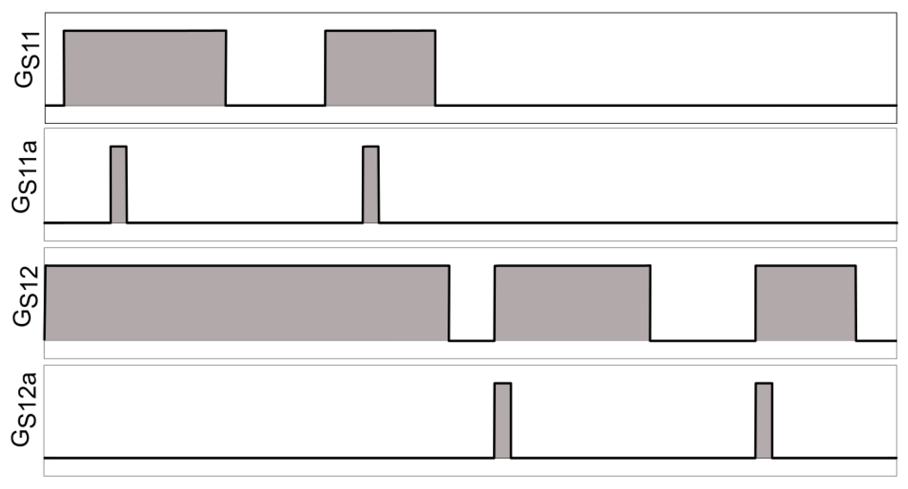
The auxiliary switches are controlled depending on the main switches (as shown in the example in Figure 7), unlike existing soft-switching systems. Auxiliary switches S11a and S14a are turned ON with a slight time delay relative to the turn-ON instants of the corresponding main switches; auxiliary switches S12a and S13a are turned ON simultaneously with the corresponding main switches S12 and S13. The turn-OFF signals of all auxiliary switches should be generated when the corresponding capacitors are discharged, and before the corresponding main switches are turned OFF. A block diagram of the control signals is shown in Figure 8.
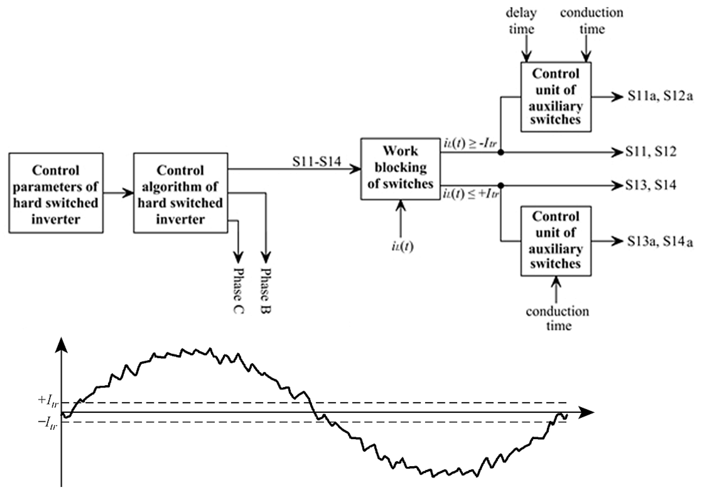
The input parameters are entered into the block “Control parameters of hard switched inverter”, which specifies the control parameters. These parameters are entered into the block “Control algorithm of hard switched inverter”, which generates a control signals for the main switches S11, S12, S13 and S14 of a 3LNPC inverter without a soft-switching system. The “Work blocking of switches” is applied to reduce additional losses that may occur in switches S13, S14, S13a and S14a when the switches S11, S12, S11a and S12a are turned ON and turned OFF. The measured instantaneous value iL(t) of the load current is compared with assumed threshold currents −Itr and +Itr. When the load current is higher than +Itr, main switches S13 and S14 and their auxiliary switches S13a and S14a are in non-conduction states. In turn, if the load current is lower than the value −Itr, switches S11, S12, S11a and S12a do not change its operating states. In the case when the instantaneous value iL(t) of the load current is in the range from −Itr to +Itr, all switches are turned ON and turned OFF. Two “Control unit of auxiliary switches” blocks generate control signals for auxiliary switches depending on the control signals of the main switches.

3. Selection of Inverter Elements

3.1. Selection of Switches

The switches in 3LNPC inverters are selected for a single supply voltage UDC. Owing to the working principles of the proposed solution, the switches should be selected for rated voltages higher than the supply voltage UDC. This especially concerns switches S11 and S14, because the maximum voltage of switches S12 and S13 is not higher than twice the value UDC.
The turn-OFF process of the main switches has a soft character, given that the maximum voltage of capacitors C11 and C14 should not be less than twice the voltage UDC. The maximum current values of switches S11, S14, and S12, S13 are determined using Equations (12), (13), and (25), (26), respectively. The auxiliary switches conduct significantly less than the main switches. Consequently, their conduction losses are relatively small. Notably, the maximum current of switches in a 3LNPC inverter with hard-switching method is the sum of the load current and the current of either the freewheeling diode or clamping diode at the given phase. The necessity to select switches for a voltage twice as high as the rated voltage is a certain inconvenience of the proposed soft-switching solution.

3.2. Reactive Elements

If ISon1 denotes the maximum current value after the turn-ON process of the main switch, then using Equation (7), the following expression can be derived for inductance L11,14 of inductors L11 and L14:
L 11 , 14 = U D C I S o n 1 t r ,
where tr denotes the so-called rise time defined in the datasheets of the selected switches.
Based on Equation (20), the inductance of inductors L12 and L13 can be determined using an analogous formula:
L 12 , 13 = U D C I S o n 2 t r ,
where ISon2 denotes the current of switches S12 and S13 after their turn-ON process. Both currents ISon1 and ISon2 can have the same value in individual cases.
Capacitors C11 and C14 are charged with constant load currents until their voltages are lower than UDC. Therefore, capacitance of these capacitors can be determined as follows:
C 11 , 14 = I L max U C O F F t f ,
where UCOFF denotes an assumed maximum capacitor voltage at the end of the main switch turn-OFF process, and tf is the so-called fall time defined in the datasheets of switching elements.
The turn-OFF process of the main switches has a soft character if the capacitor voltages are equal to zero before these switches are turned OFF. Hence, the maximum capacitor voltage should be at least 2UDC.
Assuming the maximum capacitor voltage as kmaxUDC and using Equation (5), the following additional condition concerning capacitance C11,14 must be set:
C 11 , 14 = L 11 , 14 I L max k max 1 U D C 2 .
To determine this capacitance, the value UCOFF, which is not higher than, e.g., 10% of supply voltage UDC, should be assumed. Next, using Equation (29), the minimum capacitance C11,14 should be calculated. For the assumed coefficient kmax, capacitance C11,14 should be also determined using Equation (30). If this capacitance is higher than the value resulting from Equation (29), then the first capacitance should be accepted. Otherwise, the inductance L11,14 should be increased so that capacitances determined from Equations (29) and (30) are the same.
Capacitance C12,13 of capacitors C12 and C13 is determined similarly. However, the maximum voltage of these capacitors is not higher than twice UDC, as mentioned above.

4. Laboratory Research

A three-phase 3LNPC laboratory inverter was built to verify the correctness of the presented solution. The rated power of the prototype was 3 kW, and IGBTs type G4PH50KD (Table 1) were applied in this laboratory inverter.
This inverter was supplied by a dual voltage source of 150 V; the admissible load current was 12 A. The three-phase star-connected inductive-resistive load (R = 12.2 Ω, L = 3.1 mH) was supplied by the laboratory inverter. Laboratory tests were performed with the assumption that the switch current during the turn-ON processes should be lower than 10% of the maximum load current, and the switch voltage during the turn-OFF processes should not be higher than 10% of the single supply voltage of 150 V. If the times tr and tf of a certain switch are equal to 1 µs, the inductances are as follows: L11, L14 = 120 μH, L12, L13 = 300 μH; all capacitances are equal to 1 μF. Laboratory research was performed for an output frequency of 50 Hz and switching frequencies of 500 Hz and 1 kHz.
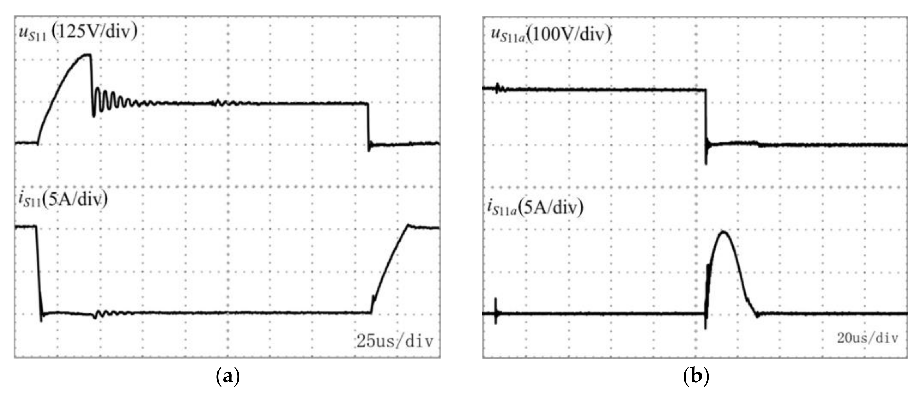
Figure 9 shows the waveforms of voltages and currents of switches S11 and S11a. At approximately 14 μs, switch S11 is turned OFF, and capacitor C11 starts to be charged with a constant load current. The voltage of switch S11 rises slowly and reaches 14 V after the turn-OFF process is ended. Both the capacitor voltage and voltage of switch S11 exceeds twice the supply voltage UDC (255 V) after the charging process. At approximately 202 μs, this switch is turned ON again. Its voltage suddenly drops to zero, whilst the current of this switch rises almost linearly from zero, and it reaches 1.6 A after the turn-ON process. Figure 9b shows waveforms of switch S11a during the resonant discharge of capacitor C11. The shapes of both the capacitor current and the current of auxiliary switch S11a are the same. Capacitor C11 discharges partly through L11, UDC1, and D11a, and partly through S11, L12, D1p, UDC1, and D12a. When the current and voltage of switch S11a equals zero, switch S11a is turned OFF.
Waveforms of the voltage and current of switch S12, and currents of inductor L12 and diode D12 are given in Figure 10. At about 170 μs, switch S12 is turned OFF, its voltage rises from zero, and the current of inductor L12 flows through diode D12 and capacitor C12. After approximately 40 μs, the processes related to the turn-OFF of switch S12. This switch is turned ON again at approximately 330 μs, and its current rises slowly to the value of the load current IL. The resonant discharge process of capacitor C12 begins at approximately 690 μs. In this case, the turn-ON of switch S12a is deliberately delayed compared to the turn-ON of switch S12 to better illustrate the operation of both switches.
Figure 11 shows the phase voltage up, phase current ip, and currents of inductors L12 and L13 measured in three output voltage periods when the inverter supplied the star-connected inductive-resistive load (R = 12.2 Ω, L = 3.1 mH).

5. Estimation of Power Losses

5.1. Numerical Analysis

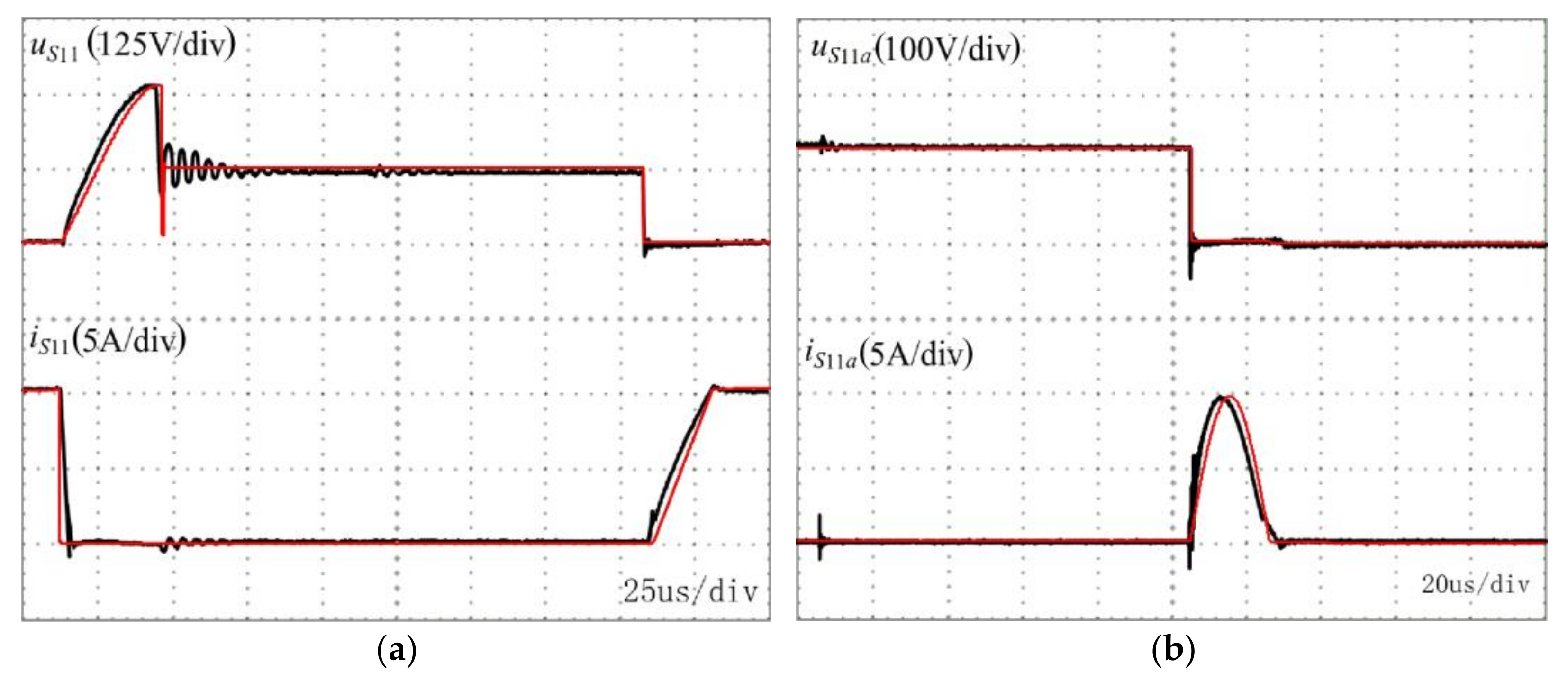
It is well known that the power losses in inverters depend on rated powers; parameters of switches also have a significant impact on these losses. It is unreasonable to build a laboratory inverter of medium- or high-power ratings with the described soft-switching solution at an initial stage of research. Therefore, the total losses were estimated based on numerical analysis using the IsSpice software, and the IGBT model described in [20] was used. This model is especially recommended to represent features of high-power transistors. The numerical model of the 3LNPC inverter was validated by comparing calculated and measured waveforms. Figure 12a shows changes in the current and voltage of switch S11 during its turn-OFF and turn-ON processes. Moreover, voltage and current waveforms of auxiliary switch S11a are presented in Figure 12b. Waveforms concerning the switching processes of S12 are also shown in Figure 13.
The turn-OFF losses of switches S11 and S12, determined from the simulation model, are equal to 7.12 µJ and 6.32 µJ, respectively, whereas the measured losses are equal to 6.74 and 5.97 µJ, respectively. The turn-ON losses of switch S11a are equal to 5.41 µJ and 5.14 µJ, respectively. Note that the turn-OFF processes of the auxiliary transistor are lossless. Calculated power losses differ from the measured values by approximately 6%.
The proposed soft-switching system can be applied especially in high-rated power inverters. Therefore, assessment of the power losses and determination of efficiency were performed for a 1.2 MW (2.35 kV) inverter. In the tested inverter, IGBTs with rated parameters 6.5 kV and 750 A (FZ750R65KE3) were applied (Table 2). The efficiency of the inverter with the proposed system was compared with the efficiency of the inverter without hard-switching. In the inverter operating without soft-switching, IGBTs (CM1500HC-90XA) with lower voltage drop in the conduction state can be used.
The squirrel cage induction motor type 6 FXA 7059 (PN = 1.15 MW, UN = 2180 V, IN = 370 A) was assumed as an inverter load. The motor equivalent circuit, based on the mathematical model described in [21], takes into account the fundamental harmonic of the air-gap magnetic field. Numerical analysis was performed for several switching frequencies. The parameters of inductors and capacitors are presented in Table 3; R11 and R12 denote resistances of inductors L11 and L12, respectively.
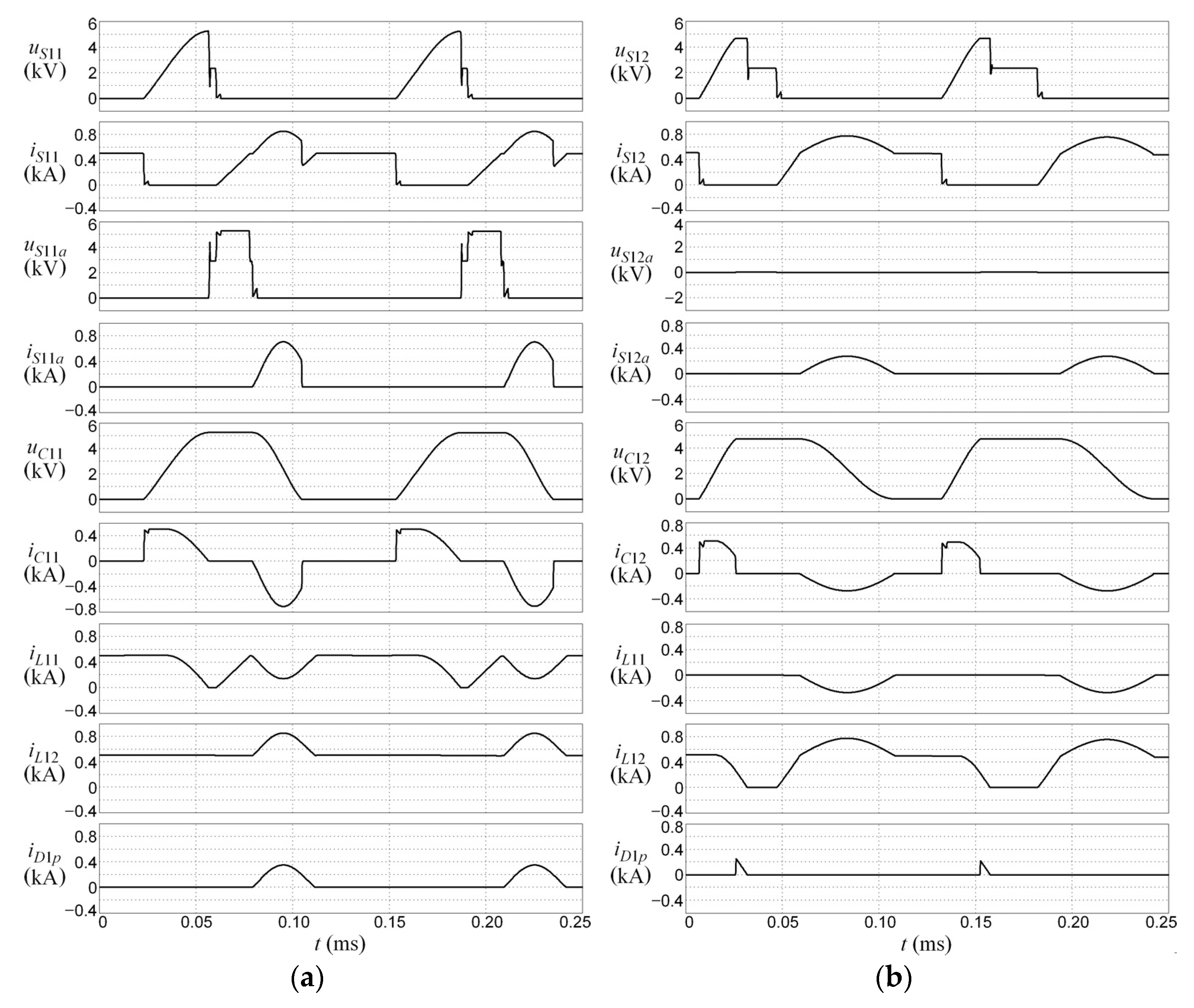
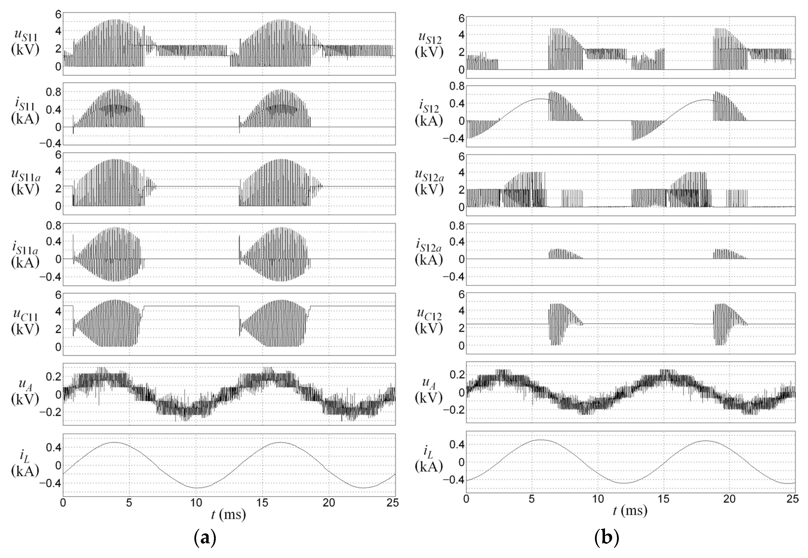
The waveforms of the inverter of rated power 1.2 MW are presented in Figure 14 and Figure 15. In practice, switch S12 is in the continuous conduction state when the system operates at a high-power factor close to unity (Figure 15a). However, when the power factor is relatively low, this switch is turned ON and turned OFF (Figure 15b). In the time interval from 6.25 ms to 8.75 ms, switch S12 is turned ON and turned OFF. The proposed soft-switching system enables significant reductions in the switching power losses. However, the effectiveness of this reduction decreases for time intervals in which the instantaneous values of the load current are relatively small. Note that VSIs typically operate as rectifiers with pulse width modulation. In this particular case, with a power factor equal to 1, switch S12 is still turned ON and turned OFF. Notably, in this case, switch S11 is almost in a non-conduction state.

5.2. Power Losses Analysis

The power losses were calculated as previously described, i.e., separately, as an integral of the product of the instantaneous voltage and current values of particular elements. Note that losses also occur in freewheeling diodes of switches and in other diodes; however, only conduction losses occur in diodes.
The losses occurring during turn-ON processes of main switches S11 and S14 depend on the inductance of inductors L11 and L14. At the beginning of the turn-OFF process of the considered switch, the voltage of the corresponding capacitor should be equal to zero. However, when the load current is relatively low, this capacitor is not discharged to zero. Then, the turn-OFF process can be partially hard. However, owing to the low load current, the switching losses occurring in this switch are relatively small. Moreover, the conduction losses also occur in auxiliary switches and their freewheeling diodes (excluding diodes DS12a and DS13a); these losses depend on the conduction time of the auxiliary switches, which in turn depend on the resonant discharge process of capacitors.
After the turn-OFF processes of main switches S11 and S14, conduction losses also occur in the freewheeling diodes of auxiliary switches DS11a and DS14a during the charging of the appropriate capacitors, i.e., C11 and C14 [22]. However, the turn-OFF losses in the mentioned diodes can be neglected owing to the occurrence of inductors. To estimate the total losses, the conduction losses in the other diodes (D11, D11a, D12, D12a, D1p, and D1n) should be taken into account. The switching losses of these diodes are negligible, as previously mentioned, owing to the nature of the changes in their currents. The conduction losses in freewheeling diodes DS11, DS12, DS13, and DS14 are also small because currents flowing through these diodes are multifold lower than the load current. Table 4 presents the particular power losses of the inverters with and without the proposed solution.
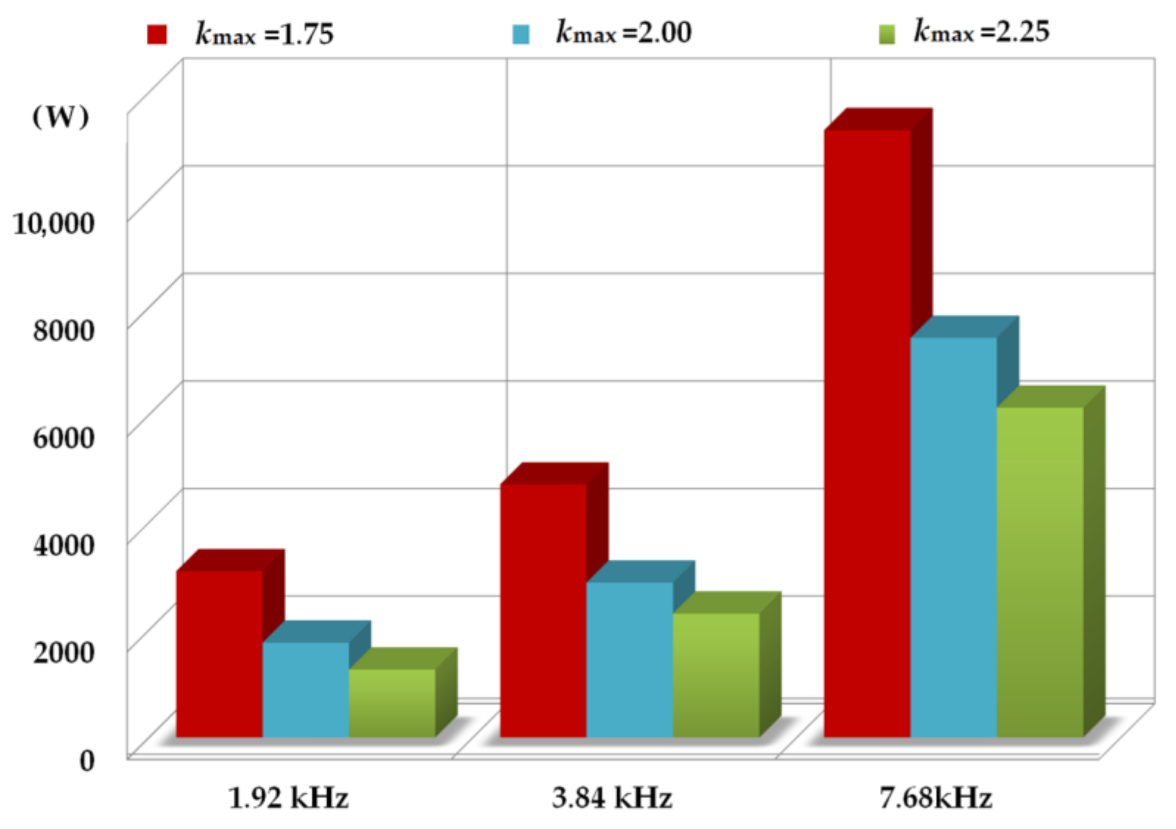
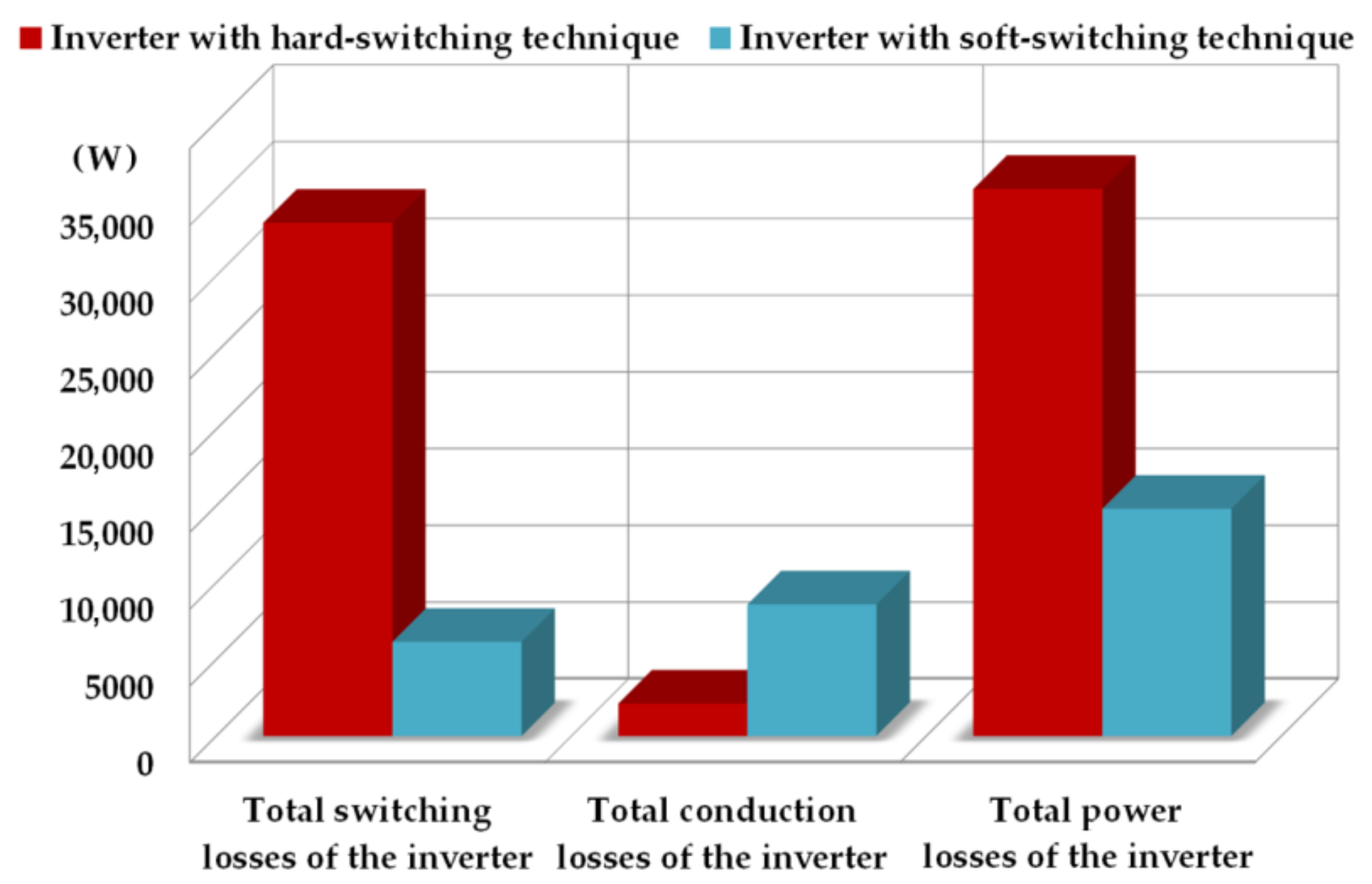
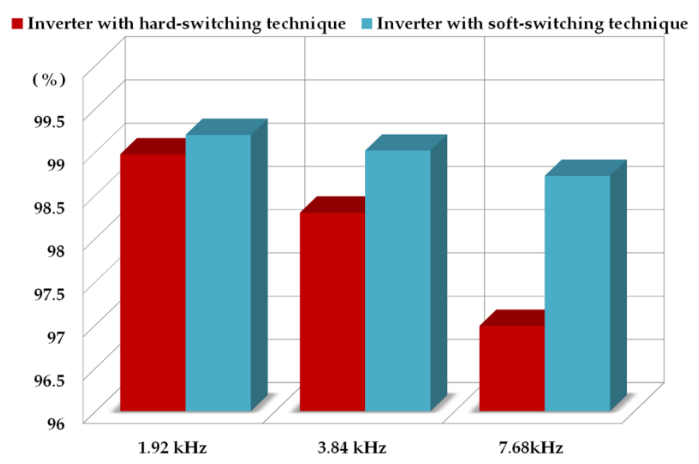
The results presented in Table 4 are partially displayed in Figure 16 and Figure 17. The inverter efficiency changes for three switching frequencies and three coefficients kmax are shown in Figure 18.
The 3LNPC inverter with the proposed solution achieved the highest efficiency for all considered values of the coefficient kmax. However, for the lowest values of the switching frequency, i.e., 1.92 kHz and coefficient kmax = 1.75, it is worth noting that the efficiency of the 3LNPC inverter with the proposed solution was almost independent on the switching frequency, whereas the efficiency of the hard switched inverter significantly decreased with the increase in this frequency. The difference between efficiencies of both types of mentioned inverters was approximately 2%.
The proposed soft-switching system allows increasing the efficiency for each assumed coefficient kmax, despite the fact that transistors applied in the proposed solution should have a higher rated voltage than transistors in inverters with hard-switching techniques; this results in slightly higher conduction losses in the proposed solution. Even after taking into account the losses in additional elements of the proposed solution, and the higher conduction losses of the main transistors for a coefficient kmax = 1.75 and the lowest assumed switching frequency of 1.92 kHz, the application of the proposed solution allows reducing the total losses by approximately 8% compared to the hard-switched inverter. The efficiency of inverters operating with the proposed solution increases with the switching frequency; when this frequency is equal to 7.68 kHz, the use of the proposed solution results in decreasing the overall inverter losses approximately 45.5% for kmax = 1.75, and approximately 58% for kmax = 2.25 in comparison to the hard-switching method.
The 3LNPC inverters with soft-switching systems, presented in the literature over the last 10 years, have the highest efficiency in the range from 92.0% to 98.3% [11,12,15,16]; however, the rated powers of these systems are from 2 to 20 kW and their structures significantly vary with respect to the proposed solution. Therefore, it is difficult to compare the efficiency of the described solution with other soft-switching systems, especially because the parameters of the switches used today, e.g., voltage drops and switching times, are more favourable than a few years ago. Moreover, these systems often have transformer couplings inside soft-switching systems or between inverters and the load [10,11,13,16]. Significant inconveniencies of soft-switching systems proposed so far concern connections between capacitors, inductors, and switches. In systems described in [10,13,14,15,16], capacitors are connected in parallel to main switches. Note that in some low-rated power inverters, parasitic capacitances of a given switch are used, but this refers to soft-switching systems with MOSFETs [11,12,13]. In case of disturbances, a given switch may be turned ON when the capacitor is not discharged; it can cause damage of the inverter. Disturbances in the inverter operation may cause an uncontrolled turn-OFF of main switches which are connected in series with transformer windings [10] or with a resistance-inductive load [11,12]. Additionally, due to different disturbances, an uncontrolled turn-OFF of auxiliary switches, which are connected in series with inductors, may occur. In this case, overvoltage appears, which is generally dangerous for semiconductor elements. Notably, in the proposed soft-switching solution, the mentioned dangers to the inverter operation do not occur.
The control system of the main switches of the proposed solution is essentially similar to that of the inverter with hard-switching. The modification of the control system mainly concerns the auxiliary switches; as a result, the control algorithm of the 3LNPC inverter is relatively simple.

6. Conclusions

In the presented soft-switching system for three-phase 3LNPC voltage source inverters, parallel connections of capacitors with main switches and series connections of inductors with auxiliary switches do not exist. Therefore, there is no risk of damage to the switches by a sudden capacitor discharge or by interruption of the current flowing through inductors; it significantly increases the reliability of inverters with the described soft-switching solution. It is worth emphasising that the auxiliary switches are controlled depending on the turn-ON and turn-OFF signals of the main switches; this makes the control system relatively simple.
The switching processes of all switches are soft, which leads to a significant reduction in the switching losses. Consequently, the efficiency of the three-phase three-level inverter is higher than the inverter operating with the hard-switching technique.
Note that the proposed soft-switching systems have certain limitations on the operation parameters, such as switching frequency, modulation depth factor; however, this feature is related to all soft-switching solutions.

Author Contributions

Conceptualisation, Z.S., B.R. and W.M.; methodology, Z.S. and W.M.; formal analysis, Z.S., and B.R.; software, Z.S.; investigation, Z.S. and W.M.; validation, Z.S., B.R. and W.M.; writing—original draft preparation, B.R. and W.M.; writing—review and editing, B.R. and W.M. All authors have read and agreed to the published version of the manuscript.

Funding

This research was funded by the Polish Ministry of Science and Higher Education and performed by the Institute of Electromechanical Energy Conversion (E22, E23) of Cracow University of Technology.

Institutional Review Board Statement

Not applicable.

Informed Consent Statement

Not applicable.

Conflicts of Interest

The authors declare no conflict of interest.

References

  1. Feix, G.; Dieckerhoff, S.; Allmeling, J.; Schonberger, J. Simple methods to calculate IGBT and diode conduction and switching losses. In Proceedings of the 13th European Conference on Power Electronics and Applications, Barcelona, Spain, 8–10 September 2009; pp. 1–8. [Google Scholar]
  2. Sadigh, A.K.; Dargahi, V.; Corzine, K.A. Investigation of conduction and switching power losses in modified stacked multicell converters. IEEE Trans. Ind. Electron. 2016, 63, 7780–7791. [Google Scholar] [CrossRef]
  3. Oñederra, O.; Kortabarria, I.; Martínez de Alegría, I.; Andreu, J.; Gárate, J.I. Three-Phase VSI optimal switching loss reduction using variable switching frequency. IEEE Trans. Power Electron. 2017, 32, 6570–6576. [Google Scholar] [CrossRef]
  4. Chang, J.; Hu, J. Modular design of soft-switching circuits for two-level and three-level inverters. IEEE Trans. Power Electron. 2006, 21, 131–139. [Google Scholar] [CrossRef]
  5. Ge, Q.; Li, Y.; Kong, L. Investigation of topologies for IGCT three-level inverter. In Proceedings of the 2008 IEEE International Conference on Industrial Technology, Chengdu, China, 21–24 April 2008; pp. 1–5. [Google Scholar]
  6. He, N.; Chen, Y.; Xu, D.; Ma, K.; Blaabjerg, F. A new zero voltage switching three-level NPC inverter. In Proceedings of the 2015 IEEE Applied Power Electronics Conference and Exposition, Charlotte, NC, USA, 15–19 March 2015; pp. 2309–2316. [Google Scholar]
  7. Song, B.; Kim, J.; Lai, J.; Seong, K.; Kim, H.; Park, S. A multilevel soft-switching inverter with inductor coupling. IEEE Trans. Ind. Appl. 2001, 37, 628–636. [Google Scholar] [CrossRef]
  8. Ghodke, D.V.; Chatterjee, K.; Fernandes, B.G. Three-Phase three level, soft switched, phase shifted PWM DC-DC converter for high power applications. IEEE Trans. Power Electron. 2008, 23, 1214–1227. [Google Scholar] [CrossRef] [Green Version]
  9. Li, J.; Liu, J.; Boroyevich, D.; Mattavelli, P.; Xue, Y. Three-Level active neutral-point-clamped zero-current-transition converter for sustainable energy systems. IEEE Trans. Power Electron. 2011, 26, 3680–3693. [Google Scholar] [CrossRef]
  10. Sahin, Y.; Ting, N.S.; Akboy, E.; Aksoy, I. A new soft switching three level T-type inverter. In Proceedings of the 10th International Conference on Compatibility, Power Electronics and Power Engineering, Bydgoszcz, Poland, 29 June–1 July 2016; pp. 314–318. [Google Scholar]
  11. Pal, A.; Basu, K. A unidirectional single-stage three-phase soft-switched isolated DC-AC converter. IEEE Trans. Power Electron. 2019, 34, 1142–1158. [Google Scholar] [CrossRef]
  12. Pal, A.; Basu, K. A three-phase three-level isolated DC-AC converter with line frequency unfolding. IEEE Trans. Power Electron. 2020, 35, 11758–11769. [Google Scholar] [CrossRef]
  13. Jang, Y.; Jovanovic, M.M. A new three-level soft-switched converter. IEEE Trans. Power Electron. 2005, 20, 75–81. [Google Scholar] [CrossRef] [Green Version]
  14. Kollensperger, P.; Lenke, R.; Schroder, S.; De Doncker, R.W. Design of a flexible control platform for soft-switching multi-level inverters. In Proceedings of the IEEE 36th Power Electronics Specialists Conference, Dresden, Germany, 16 June 2005; pp. 915–921. [Google Scholar]
  15. Gekeler, M.W. Soft switching three level inverter with passive snubber circuit (S3L inverter). In Proceedings of the 14th European Conference on Power Electronics and Applications, Birmingham, UK, 30 August–1 September 2011; pp. 1–10. [Google Scholar]
  16. Ning, G.; Chen, W.; Shu, L.; Zhao, J.; Cao, W.; Mei, J.; Liu, C.; Qiao, G. A hybrid resonant ZVZCS three-level converter for MVDC-connected OFFshore wind power collection systems. IEEE Trans. Power Electron. 2018, 33, 6633–6645. [Google Scholar] [CrossRef]
  17. Mazgaj, W.; Rozegnał, B.; Szular, Z. The System of Soft Switching of Transistors in the Three-Phase, Three-Level Voltage Source Inverter. Patent PL 232303 B1, 17 July 2017. [Google Scholar]
  18. Mazgaj, W.; Szular, Z.; Woszczyna, B. The System of Soft Switching of Thyristors in the Three-Phase, Three-Level Voltage Source Inverter. Patent PL 232304 B1, 17 July 2017. [Google Scholar]
  19. Mazgaj, W.; Szular, Z.; Woszczyna, B. New soft switching system for three-phase three-level voltage source inverters. In Proceedings of the 20th European Conference on Power Electronics and Applications (EPE’18 ECCE Europe), Riga, Latvia, 17–21 September 2018; pp. 83–92. [Google Scholar]
  20. Chimento, F.; Mora, N.; Bellini, M.; Stevanovic, I.; Tomarchio, S. A simplified spice based IGBT model for power electronics modules evaluation. In Proceedings of the IECON 2011—37th Annual Conference of the IEEE Industrial Electronics Society, Melbourne, Australia, 7–10 November 2011; pp. 1155–1160. [Google Scholar]
  21. Cholewa, D.; Mazgaj, W.; Szular, Z. Cooperation between vector controlled cage induction motor and voltage source inverter operating with soft switching system. In Proceedings of the 2018 International Symposium on Electrical Machines (SME), Andrychow, Poland, 10–13 June 2018; pp. 1–5. [Google Scholar]
  22. Haaf, P.; Harper, J. Understanding Diode Reverse Recovery and Its Effect on Switching Losses. In Proceedings of the Fairchild Power Seminar, Charlotte, NC, USA, 16 September 2008; Fairchild Semiconductor Europe: Aschheim, Germany, 2007; pp. 23–33. [Google Scholar]
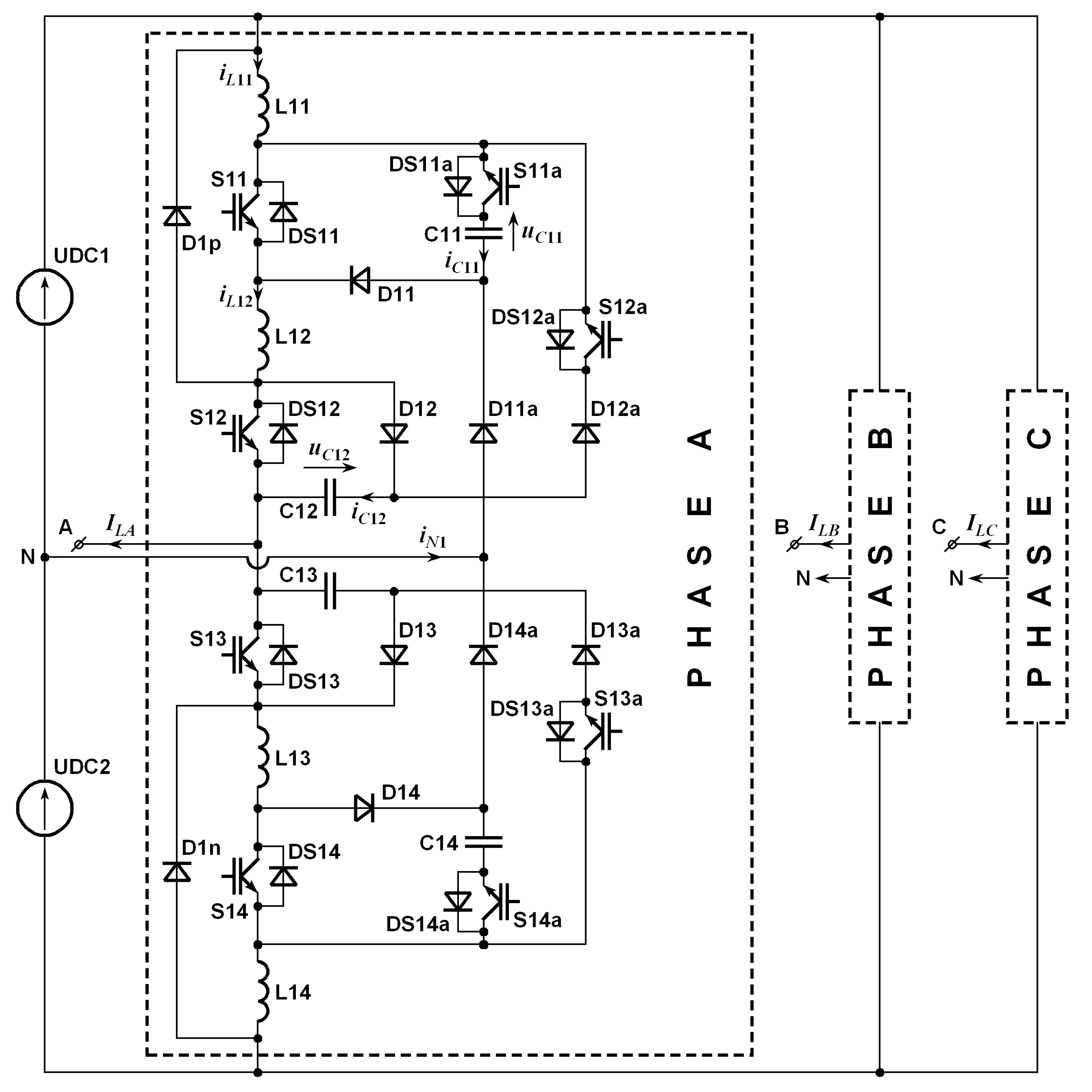
Figure 1. One phase of a three-phase three-level neutral-point-clamped (3LNPC) inverter with the proposed soft-switching system; A, B, C—load terminals; N—neutral point.
Energies 14 02247 g001
Figure 2. Simplified waveforms when S11 is switched ON/OFF: uGS11, uGS11a—control signals of switches S11 and S11a, respectively; iS11, uS11—current and voltage of switch S11, respectively; uS11a—voltage of switch S11a; iC11, uC11—current and voltage of capacitor C11, respectively; iL11, iL12—currents of inductors L11 and L12, respectively; iD11, iD12, iD1p—current of diodes D11, D12, D1p, respectively; iN1—neutral conductor current; IL—load current.
Energies 14 02247 g002
Figure 3. Operation stages when S11 is switched ON/OFF in individual time intervals: (a) before time t11; (b) t11t12; (c) t12t13; (d) t13t14; (e) t14t15; (f) t16t17; (g) t17t18.
Energies 14 02247 g003aEnergies 14 02247 g003b
Figure 4. Currents in the stage t16t17; directions of currents and voltages according to Figure 1.
Energies 14 02247 g004
Figure 5. Simplified waveforms when S12 is switched ON/OFF: uGS12, uGS12a—control signals of switches S12 and S12a, respectively; iS12, uS12—current and voltage of switch S12, respectively; iS12a—current of switch S12a; iL12—current of inductor L12; iC12 uC12—current and voltage of capacitor C12, respectively; iD11, iD12 iD1n—current of diodes D11, D12, and D1n, respectively.
Energies 14 02247 g005
Figure 6. Operation stages when S12 is switched ON/OFF in individual time intervals: (a) before time t21; (b) t21t22; (c) t22t23; (d) t23t24; (e) t24t25; (f) t25t26; (g) t26t27.
Energies 14 02247 g006aEnergies 14 02247 g006b
Figure 7. Control signals of switches S11 and S12, and their auxiliary switches S11a and S12a.
Energies 14 02247 g007
Figure 8. Generation of control signals of switches.
Energies 14 02247 g008
Figure 9. Waveforms of (a) switch S11, and (b) switch S11a; C11 = C12 = C13 = C14 = 1.0 μF; L11 = L14 = 120 μH, L12 = L13 = 300 μH, switching and output frequency of 500 Hz and 50 Hz, respectively, and modulation depth factor of 0.8.
Energies 14 02247 g009
Figure 10. Waveforms of (a) voltage and current of switch S12, and (b) currents of inductor L12 and diode D12; the measurements were made for the same parameters as in Figure 9.
Energies 14 02247 g010
Figure 11. Waveforms of (a) phase voltage up, phase current ip, and (b) currents of inductors L12 and L13 measured at a switching frequency of 1 kHz when the inverter supplied the star-connected inductive-resistive load; the operation parameters are the same as those in Figure 9.
Energies 14 02247 g011
Figure 12. Comparison of measured (black lines) and calculated (red lines) voltage and current waveforms of (a) main switch S11, and (b) auxiliary switch S11a.
Energies 14 02247 g012
Figure 13. Comparison of measured (black lines) and calculated (red lines) waveforms of (a) main switch S12, and (b) inductor L12 and diode D12, respectively.
Energies 14 02247 g013
Figure 14. Waveforms during two switching cycles when the inverter supplied the induction motor: (a) S11 is switched ON/OFF, and (b) S12 is switched ON/OFF; switching frequency: 7.68 kHz.
Energies 14 02247 g014
Figure 15. Waveforms during two output frequency periods when the power factor is equal to (a) 0.87, and (b) 0.089 (motor idle); uA, iL—motor phase voltage and current, respectively; modulation depth factor is equal to 0.85.
Energies 14 02247 g015
Figure 16. Total switching losses as a function of both the switching frequency and coefficient kmax for the 1.2 MW inverter.
Energies 14 02247 g016
Figure 17. Comparison of the switching losses, conduction losses, and total power losses; switching frequency: 7.68 kHz, kmax = 2.25.
Energies 14 02247 g017
Figure 18. Efficiencies for 1.2 MW inverters; kmax = 2.25.
Energies 14 02247 g018
Table 1. Parameters of insulated gate bipolar transistors (IGBT) type G4PH50KD.
VCC
(V)
IC
(A)
ton
(ns)
tr
(ns)
toff
(ns)
tf
(ns)
trr
(ns)
Irrm
(A)
VCE
(V)
120024.013972.07003901648.302.77
Table 2. Parameters of IGBTs.
TypeVCC
(V)
IC
(A)
ton
(μs)
tr
(μs)
toff
(μs)
tf
(μs)
trr
(μs)
Irrm
(A)
VCE
(V)
FZ750R65KE365007501.200.408.100.501.3312003.7
CM1500HC-90XA450015000.800.257.700.501.6021002.8
Table 3. Parameters of inductors and capacitors.
kmaxL11, L12 (μH)R11, R12 (mΩ)C11, C12 (μF)
1.7517.60.791.6
2.0022.00.881.1
2.2534.01.101.1
Table 4. Comparison of power losses.
kmax1.92 kHz3.84 kHz7.68 kHz
Soft
-Switching
Hard
-Switching
Soft
-Switching
Hard
-Switching
Soft
-Switching
Hard
-Switching
Total Switching Losses (W)
2.2513579733239917,700622933,542
2.00185929757531
1.753186480211,392
Conduction Losses of Transistors and Diodes (W)
2.25678122367824224177852205
2.00636774907943
1.75673662577905
Total Conduction Losses of Inductors (W)
2.251212---1242---887---
2.0011311170816
1.7510651098695
Total Power Losses of the Inverter (W)
2.25934911,96911,46519,94014,90135,747
2.00935711,63516,290
1.7510,98813,78919,486
Efficiency (%)
2.2599.1998.9799.0198.3098.7296.99
2.0099.1999.0098.60
1.7599.0598.8298.33
Publisher’s Note: MDPI stays neutral with regard to jurisdictional claims in published maps and institutional affiliations.