Article

A Hybrid Hole Transport Layer for Perovskite-Based Solar Cells

by
Joseph Asare
1,
Dahiru M. Sanni
2,
Benjamin Agyei-Tuffour
3,4,*,
Ernest Agede
1,
Oluwaseun Kehinde Oyewole
4,
Aditya S. Yerramilli
5 and
Nutifafa Y. Doumon
6,7,*
1
Department of Physics, School of Physical and Mathematical Sciences, College of Basic and Applied Sciences, University of Ghana, Legon, Accra LG 63, Ghana
2
Department of Theoretical and Applied Physics, African University of Science and Technology, Km 10 Airport Road, Abuja, FCT 900001, Nigeria
3
Department of Materials Science and Engineering, School of Engineering Sciences, College of Basic and Applied Sciences, University of Ghana, Legon, Accra LG 77, Ghana
4
Program in Materials Science and Engineering, Department of Mechanical Engineering, Worcester Polytechnic Institute, Worcester, MA 01609, USA
5
School for Engineering of Matter, Transport and Energy, Arizona State University, Phoenix, AZ 85282, USA
6
Key Laboratory of Functional Materials Physics and Chemistry of the Ministry of Education, Jilin Normal University, Changchun 130103, China
7
INRS—Centre Energie Matériaux Télécommunications, 1650 Boulevard Lionel Boulet, Varennes, QC J3X 1S2, Canada
*
Authors to whom correspondence should be addressed.
Energies 2021, 14(7), 1949; https://doi.org/10.3390/en14071949
Submission received: 27 January 2021 / Revised: 8 March 2021 / Accepted: 22 March 2021 / Published: 1 April 2021
(This article belongs to the Special Issue Advanced Polymer and Perovskite Solar Cells)

Abstract

:
This paper presents the effect of a composite poly(3,4-ethylenedioxythiophene) polystyrene sulfonate PEDOT:PSS and copper-doped nickel oxide (Cu:NiOx) hole transport layer (HTL) on the performance of perovskite solar cells (PSCs). Thin films of Cu:NiOx were spin-coated onto fluorine-doped tin oxide (FTO) glass substrates using a blend of nickel acetate tetrahydrate, 2-methoxyethanol and monoethanolamine (MEA) and copper acetate monohydrate. The prepared solution was stirred at 65 °C for 4 h and spin-coated onto the FTO substrates at 3000 rpm for 30 s in a nitrogen glovebox. The Cu:NiOx/FTO/glass structure was then annealed in air at 400 °C for 30 min. A mixture of PEDOT:PSS and isopropyl alcohol (IPA) (in 1:0.05 wt%) was spun onto the Cu:NiOx/FTO/glass substrate at 4000 rpm for 60 s. The multilayer structure was annealed at 130 °C for 15 min. Subsequently, the perovskite precursor (0.95 M) of methylammonium iodide (MAI) to lead acetate trihydrate (Pb(OAc)2·3H2O) was spin-coated at 4000 rpm for 200 s and thermally annealed at 80 °C for 12 min. The inverted planar perovskite solar cells were then fabricated by the deposition of a photoactive layer (CH3NH3PbI3), [6,6]-phenyl C61-butyric acid methyl ester (PCBM), and a Ag electrode. The mechanical behavior of the device during the fabrication of the Cu:NiOx HTL was modeled with finite element simulations using Abaqus/Complete Abaqus Environment CAE. The results show that incorporating Cu:NiOx into the PSC device improves its density–voltage (J–V) behavior, giving an enhanced photoconversion efficiency (PCE) of ~12.8% from ~9.8% and ~11.5% when PEDOT:PSS-only and Cu:NiOx-only are fabricated, respectively. The short circuit current density Jsc for the 0.1 M Cu:NiOx and 0.2 M Cu:NiOx-based devices increased by 18% and 9%, respectively, due to the increase in the electrical conductivity of the Cu:NiOx which provides room for more charges to be extracted out of the absorber layer. The increases in the PCEs were due to the copper-doped nickel oxide blend with the PEDOT:PSS which enhanced the exciton density and charge transport efficiency leading to higher electrical conductivity. The results indicate that the devices with the copper-doped nickel oxide hole transport layer (HTL) are slower to degrade compared with the PEDOT:PSS-only-based HTL. The finite element analyses show that the Cu:NiOx layer would not extensively deform the device, leading to improved stability and enhanced performance. The implications of the results are discussed for the design of low-temperature solution-processed PSCs with copper-doped nickel oxide composite HTLs.

1. Introduction

Organic–inorganic halide perovskite materials have attracted significant attention because of their excellent photoelectrical performance [1]. These materials were initially used in 2009 as semiconductor sensitizers in dye-sensitized solar cells [2,3,4,5], with a material configuration of MAPbX3, where M is the methyl (organic part), A is the ammonia (inorganic part), and X could be Br, Cl or I. The merits of these materials include solution-phase processing, intense broad-band absorption, low exciton binding energy and long charge-diffusion length [6,7,8]. These advantages have enabled perovskite materials to be rapidly developed as a new photovoltaic (PV) technology. Such perovskite materials are the most competitive absorbers for highly efficient solar cell devices [6,7,8,9,10,11]. The perovskite solar cell (PSC) has reached a power conversion efficiency (PCE) of 25.2% [12] due to its tunable bandgap, absorption coefficient, and ability to form thin films with excellent charge-carrier transport properties with an ostensive tolerance to defects [7,13,14,15]. Recent development in perovskite and silicon tandem solar cells has revealed efficiencies of 29.15% [16]. These features make such PSCs commercially promising [17,18,19].
Several techniques have been used to deposit perovskite films. These include the vapor deposition techniques [8,20,21,22,23,24]. The single-step spin and two-step sequential deposition methods are both solution-processed, cost-effective production methods. Perovskite films can be obtained from different lead sources such as lead iodide (PbI2) and lead acetate (Pb(C2H3O2)2). Recently, perovskite solar devices have been produced with lead acetate as the main source of lead [25,26]. Lead acetate has also attracted attention as a source material for perovskite solar cells because it speeds up the crystal growth of perovskite films due to the facile removal of N-methylammonium acetate (CH3NH3Ac) [27]. As a result, smooth films with fewer pinholes are obtained, which results in improved device performance.
This paper explores poly(3,4-ethylenedioxythiophene) polystyrene sulfonate-nickel oxide PEDOT:PSS/Cu:NiOx-based composites as an alternative exciton generation and transport path to improve electron blocking capability and performance compared to purely PEDOT:PSS hole injection-based devices [28]. Light passing through the transparent electrodes onto the photosensitive perovskite material (CH3NH3PbI3) stimulates excitations called electron–hole pairs. These charged particles, when separated, will diffuse through the PEDOT:PSS/Cu:NiOx composite and the [6,6]-phenyl C61-butyric acid methyl ester (PCBM) layers to their respective electrodes to generate an electric current [29]. The schematic view of the device structure is shown in Figure 1a. Note that the control devices are made of PEDOT:PSS-only and copper-doped nickel oxide (Cu:NiOx)-only. The PEDOT:PSS/Cu:NiOx composite hole transport layer is shown in Figure 1b. The device that demonstrated the best functionality was achieved with the 0.1 M Cu:NiOx composite hole transport layer (HTL).
Nickel Oxide NiO is an inorganic p-type material commonly used in semiconductor fabrication. It has a large bandgap and possesses very deep valence bands. These align perfectly with the highest occupied molecular orbital HOMO levels of a variety of organic semiconductors [28,30]. NiO has excellent energy-level alignment with the perovskite (CH3NH3PbI3) active layer. According to Kim et al. [31], when NiO is doped with copper (Cu), high-performance devices are obtained, with decent environmental stability. This is because Cu has unique electronic and structural effects and is also easy to incorporate into the solution-based fabrication of NiO [7,28,31,32]. Also, it has been noted by Chen et al. [32] that when the Cu content increases, the optical transmittance of the material reduces [32,33,34]. Photoluminescence (PL) spectroscopy results from the literature show that the PL quenching of Cu:NiOx is comparable to that of PEDOT:PSS [31]. These findings motivated the investigation of the combination of PEDOT:PSS and Cu:NiOx as a new composite hole transportation layer for the PSC, of which the authors are not aware of such study in the literature. A scanning electron microscopy cross-sectional view of the perovskite-based solar cell can be seen in Figure 1b.
The energy-level diagram of this intended device is illustrated in Figure 1c. The figure shows how the PEDOT:PSS/Cu:NiOx composite hole injection layer aligns in the PSC’s multilayer structure. The thinness of the Cu:NiOx and PEDOT:PSS results in band bending, leading to a composite energy-level prediction of ~5.3 eV for the PEDOT:PSS/Cu:NiOx-based hole injection layer. This results in a PEDOT:PSS/Cu:NiOx hole transport layer, enhancing hole collection and transport efficiency [7,31,35,36,37,38]. Therefore, interface recombination is prevented [39,40,41].

2. Materials and Methods

A fluorine-doped tin oxide (FTO)/glass substrate was procured (Guangdong Youxuan Technology, Guangdong, China) and washed with a detergent solution, deionized water, acetone and isopropyl alcohol (IPA) (Pharmco Products Inc, Brookfield, CT, USA). The substrate was ultraviolet-ozone (UV-ozone)-treated for 15 min. Two solutions of Cu:NiOx were prepared by varying the concentrations of Cu:NiOx from 0.1 M to 0.2 M. First, the 0.1 M Cu:NiOx precursor solution was prepared at 65 °C and stirred for 4 h from copper (II) acetate monohydrate (Oakwood Chemical, Columbia), nickel (II) acetate tetrahydrate, and 2-methoxyethanol (Alfa Aesar, Tewksbury, MA, USA). The precursor was subsequently deposited onto the FTO substrates at 3000 rpm for 30 s in a nitrogen glovebox. The Cu:NiOx/FTO/glass structure was then annealed in air at 400 °C for 30 min to develop Cu:NiOx nanocrystal structures. A mixture of PEDOT:PSS (Sigma Aldrich, St. Louis, MO, USA) and IPA (in 1:0.05 wt%) was filtered through a 0.45 μm polytetrafluoroethylene PTFE filter (Whatman, Buckinghamshire, UK) and spun onto the Cu:NiOx/FTO/glass substrate at 4000 rpm for 60 s. The multilayer structure was annealed on a hot plate at 130 °C for 15 min. A 5% excess lead perovskite precursor of 0.95 M was prepared in a 3:1 molar ratio of methylammonium iodide (MAI) (Dyesol, USA) to lead acetate trihydrate (Pb(OAc)2·3H2O) (Alfa Aesar, Tewksbury, MA, USA), respectively. The perovskite solution was spin-coated at 4000 rpm for 200 s and thermally annealed at 80 °C for 12 min to form the CH3NH3PbI3 crystals [4,8,42]. The various stages involved in the fabrication process are illustrated in Figure 2.
PCBM (0.02 g) (Sigma-Aldrich, St. Louis, MO, USA) in 1 mL of chlorobenzene solution was deposited onto the CH3NH3PbI3/PEDOT:PSS/Cu:NiOx/FTO/glass substrate spinning at 2000 rpm for 60 s. A 90 nm thick Ag electrode was thermally evaporated onto the active device for characterization. The configuration of the control device is Ag/PCBM/CH3NH3PbI3/PEDOT:PSS/FTO/glass.
The devices were tested under a Xenon-lamp solar simulator (Spectral Physics, Oriel Instruments, Irvine, CA, USA) [43], with a simulated Air Mass (AM) 1.5 global solar irradiation (100 mW/cm2). The current density–voltage curves of the devices were obtained from a Keithley 2400 source meter instrument. All the films produced were subjected to scanning electron microscopy (SEM) analyses, (SEM-XL30 Environmental FEG (FEI)), spectrophotometer (Cary 5000 UV/VIS spectrometer), and a Panalytical X’Pert Pro X-ray diffractometer (Almelo, The Netherlands). The steady-state photoluminescence excitation of the perovskite layers was studied using a picosecond time-correlated single-photon counting (TCSPC) spectrofluorometer.

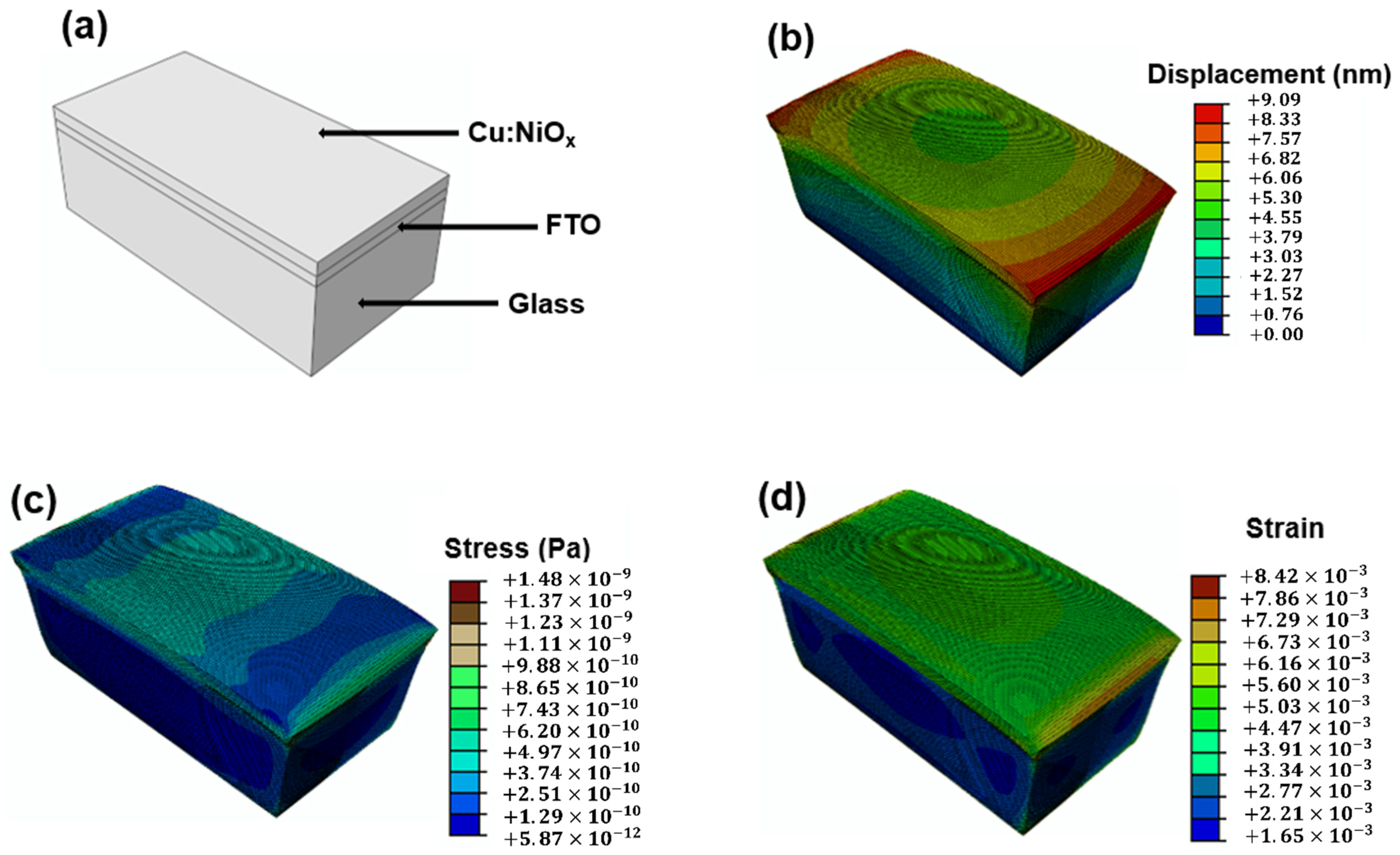
3. Finite Element Analysis Using Abaqus/CAE

Finite element analysis methods were birthed in the early 1950s by Turner et al. [44] at the Boeing Airplane Company for calculating stiffness influence coefficients of complex-type structures. In modern engineering, finite element analysis is used to solve complex structural mechanics for the structures before real field implementation. In this research, it is used to demonstrate the mechanical behavior of the device during the fabrication of the Cu:NiOx HTL when heated in air at 400 °C for 30 min.
Abaqus/CAE (Dassault Systemes, Simulia Cooperation, Providence RI, USA) was the finite element software package used to study the effect of temperature on the mechanical behavior of the annealed Cu:NiOx composite layer on the FTO-coated glass. The model partitioned in Figure 3a has an overall thickness of 1750 nm, with that of the Cu:NiOx layer (top layer) being 125 nm thick, as shown in Figure 1b. Figure 3b,c reveals the analyzed spatial displacement (deformation), strain and stress across the Cu:NiOx/FTO/glass multilayer when annealed at 400 °C. Figure 3b shows that the Cu:NiOx layer formed would not extensively deform the multilayer. The FTO layer experiences the highest strains and stresses from the heating while the glass substrate is observed to withstand most of the thermal stresses and strains achieved in Figure 3c,d [45]. This method of fabricating the Cu:NiOx HTL can also be translated onto a polymeric or flexible substrate on the condition that their thermal capacity can accommodate the high temperatures utilized here. Simulation results of the HTL on a polyethylenetherephthalate PET substrate are available in the Supplementary Materials (Figure S1) to validate this claim.

4. Results and Discussion

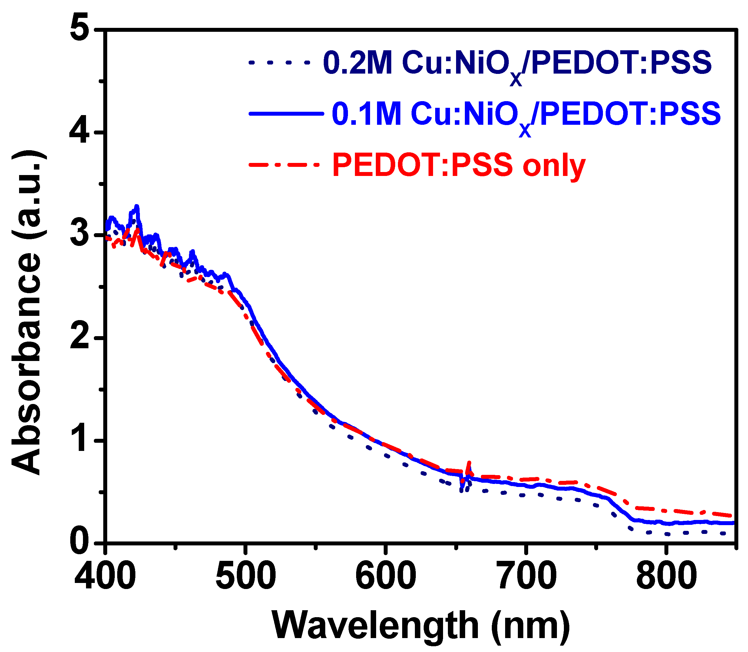
4.1. Optical Characterization

The optical characteristics of the perovskite and combined hole transport layers are presented in Figure 4. Herein, the stack layers’ optical absorbance properties are presented to show the influence induced by the respective HTLs in the perovskite devices [46]. This influence was evaluated by comparing the composite HTL (Cu:NiOx/PEDOT:PSS) with the control PEDOT:PSS-based devices. Based on the ultraviolet-visible (UV-Vis) spectroscopy characteristics, it can be seen that the absorbance was largely in the visible spectrum (~400–800 nm). The absorption profiles are similar for PEDOT:PSS, 0.1 M Cu:NiOx and 0.2 M Cu:NiOx, with the 0.1 M Cu:NiOx/PEDOT:PSS showing a marginal increase in absorbance. This shows that the composite HTLs exhibited more than 80% transmittance within the visible light spectrum and are comparable to the transmittance values of PEDOT:PSS-only [30,32,33,35,38,47,48,49,50,51,52,53,54], indicating no impediment in light transmission by the use of the composite HTL. Also, the photoluminescence spectra for the devices with different concentrations of Cu:NiOx with PEDOT:PSS and the control devices were all located at ~771 nm, indicating no red shift or blue shift (See Figure S2). This shows the bandgap in the two layers did not differ and they correspond to a bandgap of 1.61 eV [55].

4.2. Microstructures of Layered Films of Perovskite Solar Cells

The SEM images of the layered films of the perovskite solar cells are presented in Figure 5. Figure 5a–c represents the microstructure of the perovskite films on PEDOT:PSS/Cu:NiOx and PEDOT:PSS-only HTL, respectively. Similar grain sizes and aggregated appearances can be observed in all the SEM images of the perovskite layer. This suggests that the microstructure is not altered when deposited on the composite Cu:NiOx/PEDOT:PSS layer or on the control. This makes it conducive for device fabrication since a similar crystallization level of the perovskite is maintained.

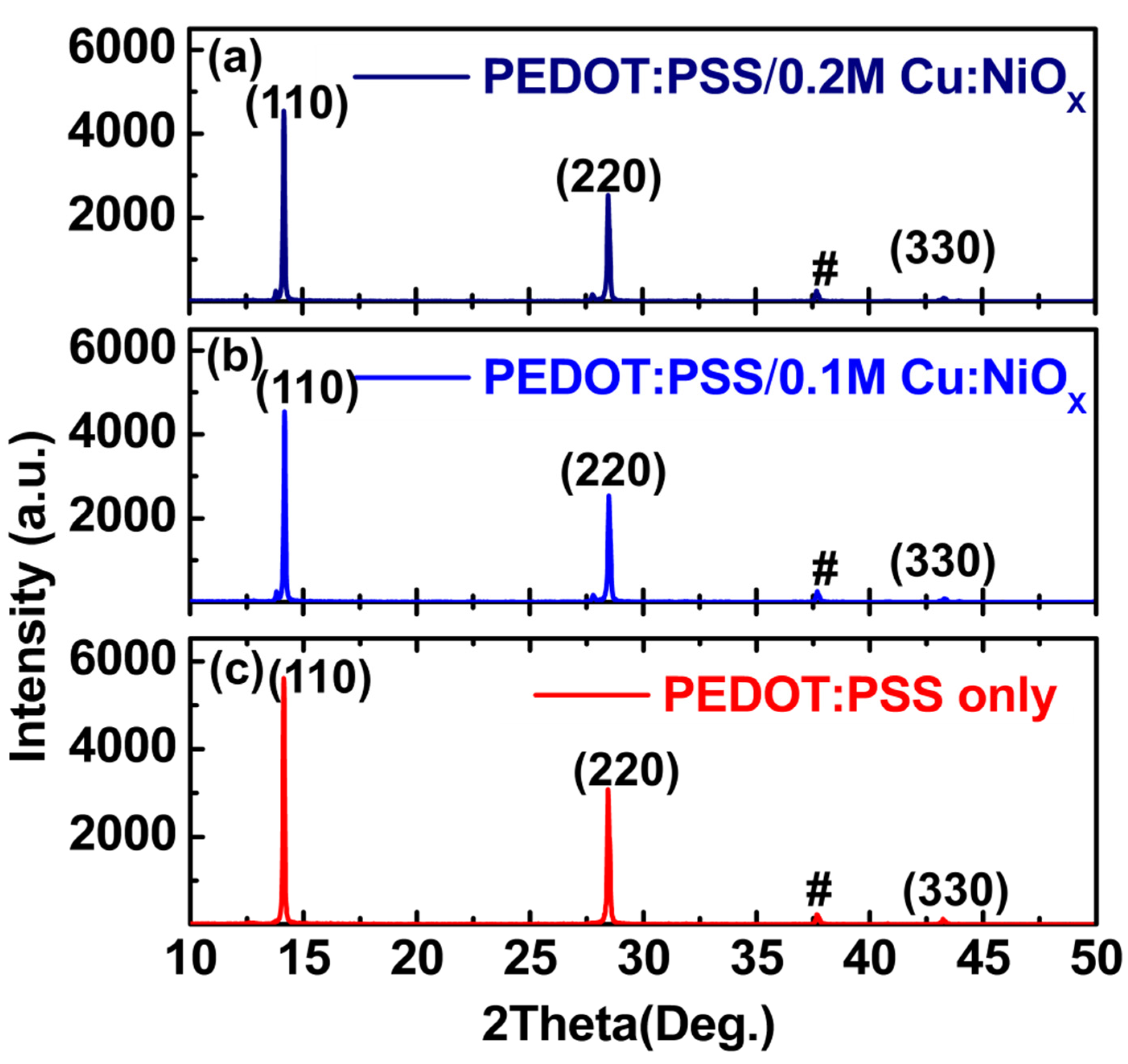
4.3. X-ray Diffraction Analysis of the Composite HTL Perovskite Solar Cells

Figure 6a–c presents the diffractograms (2 theta scans) of perovskite layers spin-coated onto the compact PEDOT:PSS/Cu:NiOx and the PEDOT:PSS-only-coated FTO glass using an X-ray diffractometer, while Figure S3 shows the Cu:NiOx-coated FTO glass. All the samples showed comparable x-ray diffraction XRD characteristics, with both 0.1 M and 0.2 M Cu:NiOx-based samples displaying the same level of intensity in the peaks. The XRD reflections confirm a CH3NH3PbI3 perovskite structure with peaks assigned to a tetragonal perovskite lattice with the following unit cell parameters: a = b = 8.85 Å, c = 12.64 Å [42,56]. The peaks marked with a “#” are assigned to the FTO [42].

4.4. Performance of Fabricated Perovskite Solar Cells

The performance of perovskite solar cells (PSCs) that were fabricated using different HTLs is presented in Figure 7. The current density–voltage (J–V) curves of the devices are shown in Figure 7a with only PEDOT:PSS and PEDOT:PSS/Cu:NiOx composite (with 0.1 M and 0.2 M concentrations of Cu:NiOx) HTLs. The results show that incorporating Cu:NiOx into the PSC device improves its J–V behavior, giving a large area under the curve. The increase in the open-circuit voltage (Voc) of the device with 0.1 M Cu:NiOx/PEDOT:PSS could result from the reduction in the potential loss at the HTL/perovskite interface due to the improved energy-level alignment, as shown by Paul et al. [39,40] and Li et al. [41] who adopted the band-bending technique to eliminate recombination at the interfaces of cadmium telluride (CdTe), thin-films and copper-indium-gallium-selenide (Cu(In,Ga)Se2) solar cells with low and high gallium (Ga) compositions. The improved Jsc of the Cu:NiOx/PEDOT:PSS could be attributed to the increase in the electrical conductivity of the Cu:NiOx, which provides room for more charges to be extracted from the perovskite absorber layer. However, the reduction in the efficiency of the 0.2 M Cu:NiOx/PEDOT:PSS as an HTL could be due to surface defects caused by excess copper used as the dopant, creating recombination sites for trapped charges. Compared to the PEDOT:PSS HTL devices, there were 18% and 9% increases in the Jsc for the 0.1 M Cu:NiOx and 0.2 M Cu:NiOx-based devices, respectively. The Jsc of the 0.2 M Cu:NiOx-based device was lower compared to that of the 0.1 M Cu:NiOx, and this could be due to the increase in charge concentration which reduces the charge mobility [32]. The efficiencies of the PEDOT:PSS with 0.1 M Cu:NiOx devices were the highest with ~12.8%, followed by the 0.2 M Cu:NiOx at ~10.1%, the PEDOT:PSS-only device at ~9.8% and ~11.5% for the Cu:NiOx-only device. The changes in these values are due to the copper-doped nickel oxide blend with the PEDOT:PSS. At this point, the hole collection is enhanced along with charge transport efficiency, leading to higher electrical conductivity.
The summary of the device parameters is presented in Table 1. It is important to note here that Figure 7a shows the J–V curves for the best device fabricated from PEDOT:PSS/Cu:NiOx HTL alongside the J–V curve from the control PEDOT:PSS HTL. The results indicate that the PEDOT:PSS/0.1 M Cu:NiOx HTL and the light absorber (CH3NH3PbI3) have perfect energy-level alignment leading to an improvement in their electron-blocking capabilities [28]. According to Uisik Kwon et al., such layer configurations result in the superior stability of the device in air than PEDOT:PSS HTL-only-based devices [28]. Figure 7b presents the PCE distribution measured for the different fabricated devices. The PCEs measured from all PEDOT:PSS/Cu:NiOx HTL-based devices and the PEDOT:PSS-only device show that PSCs with 0.1 M Cu:NiOx exhibit the best device performance overall.
The photodegradation performance of the two types of solar cells, namely PEDOT:PSS and 0.1 M Cu:NiOx/PEDOT:PSS-based devices, was also studied. The solar cells are continuously exposed at 1 sun (AM1.5G spectral irradiance) in an inert atmosphere. The photodegradation tests of the devices shown in Figure 7c reveal that devices with PEDOT:PSS/Cu:NiOx hole transport layers have a slower photodegradation rate than those of PSCs made with PEDOT:PSS-only as the hole transportation layer. The PEDOT:PSS-only-based solar cell exhibits only a lifetime (T80) of about 35 min and fully degrades at about 75 min to reach 0% of its initial efficiency. On the other hand, the Cu:NiOx/PEDOT:PSS-based cell showed improved performance, exhibiting a T80 of at least 100 min. A look at the other PV parameters shows that the fill factor (FF), shown in Figure S4, underpins the behavior of the PCE degradation curve. While the Jsc showed a faster degradation trend, the Voc showed a very steady slow degradation trend.
The fast degradation of the PEDOT:PSS-only device could be due to its acidic [58,59] and hygroscopic [60] nature, decaying the transparent conducting oxide (FTO) and/or the photoactive layer, which is sensitive to moisture. It could also be a result of morphological inhomogeneity with rougher interfaces. Figure 5a,b shows the SEM image of perovskite/PEDOT:PSS/FTO/glass and perovskite/PEDOT:PSS/0.1 M Cu:NiOx/FTO/glass, respectively. These phenomena could explain the rapid drop in Jsc and FF upon continuous illumination, previously linked to a drop in charge extraction and imbalance in charge carriers’ mobility [60,61]. Further work is needed to optimize the degradation behavior and comprehend the causes of this observed behavior. The degradation results presented here are only for the illustrations of the first few results; however, the concept proves that the use of Cu:NiOx/PEDOT:PSS as an HTL can improve both the PCE and stability of PSCs.

5. Conclusions

In this paper, the effect of a PEDOT:PSS and copper-doped nickel oxide (Cu:NiOx) composite hole transport layer (HTL) on the performance of perovskite solar cells (PSCs) has been presented. Thin films of inverted planar perovskite solar cells were fabricated by a photoactive layer (from a solution of methylammonium lead iodide (CH3NH3PbI3), [6,6]-phenyl C61-butyric acid methyl ester (PCBM), and a Ag electrode). The mechanical behavior of the device during the fabrication of the Cu:NiOx HTL was modeled with finite element simulations using Abaqus/CAE. The results showed that incorporating Cu:NiOx into the PSC devices improves its J–V behavior, giving an enhanced photoconversion efficiency (PCE) of ~12.8% from ~9.8% and ~11.5% when PEDOT:PSS-only and Cu:NiOx-only are fabricated, respectively. The Jsc for the 0.1 M Cu:NiOx and 0.2 M Cu:NiOx-based devices increased by 18% and 9%, respectively, due to the increase in the electrical conductivity of the Cu:NiOx, which provides room for more charges to be extracted from the perovskite absorber layer. The increase in the PCE was due to the copper-doped nickel oxide blend with the PEDOT:PSS, which enhanced the hole collection and charge transport efficiency leading to higher electrical conductivity. The results indicate that the devices with the copper-doped nickel oxide (Cu:NiOx) composite hole transport layer (HTL) were slower to degrade compared with the PEDOT:PSS-only-based HTL. The increase in the open-circuit voltage (Voc) of the device with 0.1 M Cu:NiOx/PEDOT:PSS was as a result of the reduction in the potential loss at the HTL/perovskite interface due to the improved energy-level alignment using the band-bending technique. The finite element analyses showed that the Cu:NiOx layer does not extensively deform the multilayer and the highest strains and stresses from the heating, while the glass substrate was observed to withstand the thermal stresses and strains. It can be deduced that low-temperature solution-processed PSCs with copper-doped nickel oxide composite HTL is a promising technique for enhancing the performance of perovskite solar cells.

Supplementary Materials

The following are available online at https://www.mdpi.com/article/10.3390/en14071949/s1, Figure S1: Simulation results of the HTL on a polyethylene terephthalate (PET), Figure S2: Photoluminescence spectra, Figure S3: X-ray diffraction spectrum of Cu:NiOx crystallographic formation on FTO coated glass, Figure S4: FF evolution over time of PEDOT:PSS and Cu:NiOx/PEDOT:PSS-based solar cells.

Author Contributions

J.A., D.M.S. and B.A.-T. conceptualized the work; D.M.S., A.S.Y. and J.A. performed the experiments; the simulation work was done by E.A. and J.A. and validated by O.K.O. and B.A.-T.; the analysis of data was done by J.A., A.S.Y., D.M.S., B.A.-T. and N.Y.D.; the original draft and preparation of the manuscript were written by J.A., D.M.S., B.A.-T. and N.Y.D.; the review and editing of the manuscript were done by J.A., A.S.Y., D.M.S., B.A.-T., O.K.O. and N.Y.D. The authors have given approval for the submission and publication of this manuscript in MDPI energies journal. All authors have read and agreed to the published version of the manuscript.

Funding

This project was funded by the BANGA-Africa programme, University of Ghana with funding from the Carnegie Corporation of New York.

Institutional Review Board Statement

Not applicable.

Informed Consent Statement

Not Applicable.

Data Availability Statement

Not applicable.

Acknowledgments

The authors acknowledge Terry Alford for providing the laboratory space and collaborative technical assistance. The Macro Technology Works, Engineering Research Center, and the LeRoy Eyring Center for Solid State Science at Arizona State University, Tempe, USA are also appreciated for their useful technical support. J. Asare and D. Sanni also acknowledge the support of the Pan African Materials Institute (PAMI) of the African University of Science and Technology (AUST), Abuja, Nigeria.

Conflicts of Interest

The authors declare no conflict of interest.

References

  1. Wang, X.; Li, M.; Zhang, B.; Wang, H.; Zhao, Y.; Wang, B. Recent progress in organometal halide perovskite photodetectors. Org. Electron. 2018, 52, 172–183. [Google Scholar] [CrossRef]
  2. Jung, H.S.; Park, N.-G. Perovskite Solar Cells: From Materials to Devices. Small 2015, 11, 10–25. [Google Scholar] [CrossRef]
  3. Snaith, H.J. Perovskites: The Emergence of a New Era for Low-Cost, High-Efficiency Solar Cells. J. Phys. Chem. Lett. 2013, 4, 3623–3630. [Google Scholar] [CrossRef]
  4. Song, T.B.; Chen, Q.; Zhou, H.; Jiang, C.; Wang, H.H.; Yang, Y.M.; Liu, Y.; You, J.; Yang, Y. Perovskite solar cells: Film formation and properties. J. Mater. Chem. A 2015, 3, 9032–9050. [Google Scholar] [CrossRef]
  5. Fan, J.; Jia, B.; Gu, M. Perovskite-based low-cost and high-efficiency hybrid halide solar cells. Photonics Res. 2014, 2, 111. [Google Scholar] [CrossRef] [Green Version]
  6. Liu, M.; Johnston, M.B.; Snaith, H.J. Efficient planar heterojunction perovskite solar cells by vapour deposition. Nature 2013, 501, 395–398. [Google Scholar] [CrossRef]
  7. Zhu, Z.; Bai, Y.; Zhang, T.; Liu, Z.; Long, X.; Wei, Z.; Wang, Z.; Zhang, L.; Wang, J.; Yan, F.; et al. High-Performance Hole-Extraction Layer of Sol-Gel-Processed NiO Nanocrystals for Inverted Planar Perovskite Solar Cells. Angew. Chem. Int. Ed. 2014, 53, 12571–12575. [Google Scholar] [CrossRef]
  8. Chen, Q.; Zhou, H.; Hong, Z.; Luo, S.; Duan, H.-S.; Wang, H.-H.; Liu, Y.; Li, G.; Yang, Y. Planar Heterojunction Perovskite Solar Cells via Vapor-Assisted Solution Process. J. Am. Chem. Soc. 2014, 136, 622–625. [Google Scholar] [CrossRef]
  9. Eperon, G.E.; Burlakov, V.M.; Docampo, P.; Goriely, A.; Snaith, H.J. Morphological Control for High Performance, Solution-Processed Planar Heterojunction Perovskite Solar Cells. Adv. Funct. Mater. 2014, 24, 151–157. [Google Scholar] [CrossRef]
  10. Handa, T.; Tex, D.M.; Shimazaki, A.; Aharen, T.; Wakamiya, A.; Kanemitsu, Y. Optical characterization of voltage-accelerated degradation in CH_3NH_3PbI_3 perovskite solar cells. Opt. Express 2016, 24, A917–A924. [Google Scholar] [CrossRef]
  11. Si, F.; Tang, F.; Xue, H.; Liu, J.L. Electronic and optical properties of CH3NH3Pb1-xAgxI3from the first-principles calculations. J. Renew. Sustain. Energy 2018, 10, 033504. [Google Scholar] [CrossRef]
  12. Saliba, M.; Etgar, L. Current Density Mismatch in Perovskite Solar Cells. ACS Energy Lett. 2020, 5, 2886–2888. [Google Scholar] [CrossRef]
  13. Yang, W.S.; Park, B.-W.; Jung, E.H.; Jeon, N.J.; Kim, Y.C.; Lee, D.U.; Shin, S.S.; Seo, J.; Kim, E.K.; Noh, J.H.; et al. Iodide management in formamidinium-lead-halide—Based perovskite layers for efficient solar cells. Science 2017, 356, 1376–1379. [Google Scholar] [CrossRef] [PubMed] [Green Version]
  14. Xu, J.; Boyd, C.C.; Yu, Z.J.; Palmstrom, A.F.; Witter, D.J.; Larson, B.W.; France, R.M.; Werner, J.; Harvey, S.P.; Wolf, E.J.; et al. Triple-Halide Wide-Band Gap Perovskites with Suppressed Phase Segregation for Efficient Tandems. Science 2020, 367, 1097–1104. [Google Scholar] [CrossRef]
  15. Mao, W.; Hall, C.R.; Chesman, A.S.R.; Forsyth, C.; Cheng, Y.B.; Duffy, N.W.; Smith, T.A.; Bach, U. Visualizing Phase Segregation in Mixed-Halide Perovskite Single Crystals. Angew. Chem. Int. Ed. 2019, 58, 2893–2898. [Google Scholar] [CrossRef]
  16. Al-Ashouri, A.; Köhnen, E.; Li, B.; Magomedov, A.; Hempel, H.; Caprioglio, P.; Márquez, J.A.; Morales Vilches, A.B.; Kasparavicius, E.; Smith, J.A.; et al. Monolithic Perovskite/Silicon Tandem Solar Cell with >29% Efficiency by Enhanced Hole Extraction. Science 2020, 370, 1300–1309. [Google Scholar] [CrossRef] [PubMed]
  17. Yang, W.S.; Noh, J.H.; Jeon, N.J.; Kim, Y.C.; Ryu, S.; Seo, J.; Seok, S.I. High-Performance Photovoltaic Perovskite Layers Fabricated through Intramolecular Exchange. Science 2015, 348, 2013–2017. [Google Scholar] [CrossRef]
  18. Liu, M.-H.; Zhou, Z.-J.; Zhang, P.-P.; Tian, Q.-W.; Zhou, W.-H.; Kou, D.-X.; Wu, S.-X. P-Type Li, Cu-Codoped NiOx Hole-Transporting Layer for Efficient Planar Perovskite Solar Cells. Opt. Express 2016, 24, 128–132. [Google Scholar] [CrossRef]
  19. Zheng, F.; Chen, W.; Bu, T.; Ghiggino, K.P.; Huang, F.; Cheng, Y.; Tapping, P.; Kee, T.W.; Jia, B.; Wen, X. Triggering the Passivation Effect of Potassium Doping in Mixed-Cation Mixed-Halide Perovskite by Light Illumination. Adv. Energy Mater. 2019, 9, 1–11. [Google Scholar] [CrossRef]
  20. Docampo, P.; Ball, J.M.; Darwich, M.; Eperon, G.E.; Snaith, H.J. Efficient Organometal Trihalide Perovskite Planar-Heterojunction Solar Cells on Flexible Polymer Substrates. Nat. Commun. 2013, 4, 4. [Google Scholar] [CrossRef] [PubMed] [Green Version]
  21. Kim, H.-S.; Lee, C.-R.; Im, J.-H.; Lee, K.-B.; Moehl, T.; Marchioro, A.; Moon, S.-J.; Humphry-Baker, R.; Yum, J.-H.; Moser, J.E.; et al. Lead Iodide Perovskite Sensitized All-Solid-State Submicron Thin Film Mesoscopic Solar Cell with Efficiency Exceeding 9%. Sci. Rep. 2012, 2, 1–7. [Google Scholar] [CrossRef] [PubMed] [Green Version]
  22. Heo, J.H.; Im, S.H.; Noh, J.H.; Mandal, T.N.; Lim, C.S.; Chang, J.A.; Lee, Y.H.; Kim, H.J.; Sarkar, A.; Nazeeruddin, M.K.; et al. Efficient Inorganic-Organic Hybrid Heterojunction Solar Cells Containing Perovskite Compound and Polymeric Hole Conductors. Nat. Photonics 2013, 7, 1–6. [Google Scholar] [CrossRef]
  23. Burschka, J.; Pellet, N.; Moon, S.J.; Humphry-Baker, R.; Gao, P.; Nazeeruddin, M.K.; Grätzel, M. Sequential Deposition as a Route to High-Performance Perovskite-Sensitized Solar Cells. Res. Lett. 2013, 499, 316–319. [Google Scholar] [CrossRef]
  24. Shrivastava, P.; Balasubramaniam, K.R.; Bhargava, P. Effect of Br-Doping and Choice of Precursor Solvent on Morphology of Lead Free (CH3NH3)3Bi2I9 Perovskites. J. Renew. Sustain. Energy 2018, 10, 043506. [Google Scholar] [CrossRef]
  25. Sanni, D.M.; Chen, Y.; Yerramilli, A.S.; Ntsoenzok, E.; Asare, J.; Adeniji, S.A.; Oyelade, O.V.; Fashina, A.A.; Alford, T.L. An Approach to Optimize Pre-Annealing Aging and Anneal Conditions to Improve Photovoltaic Performance of Perovskite Solar Cells. Mater. Renew. Sustain. Energy 2019, 8, 3. [Google Scholar] [CrossRef] [Green Version]
  26. Yerramilli, A.S.; Chen, Y.; Sanni, D.; Asare, J.; Theodore, N.D.; Alford, T.L. Impact of Excess Lead on the Stability and Photo-Induced Degradation of Lead Halide Perovskite Solar Cells. Org. Electron. Phys. Mater. Appl. 2018, 59, 107–112. [Google Scholar] [CrossRef]
  27. Qing, J.; Chandran, H.T.; Cheng, Y.H.; Liu, X.K.; Li, H.W.; Tsang, S.W.; Lo, M.F.; Lee, C.S. Chlorine Incorporation for Enhanced Performance of Planar Perovskite Solar Cell Based on Lead Acetate Precursor. ACS Appl. Mater. Interfaces 2015, 7, 23110–23116. [Google Scholar] [CrossRef]
  28. Kwon, U.; Kim, B.; Nguyen, D.C.; Park, J.; Ha, N.Y.; Kim, S.-J.; Ko, S.H.; Lee, S.; Lee, D.; Park, H.J. Solution-Processible Crystalline NiO Nanoparticles for High-Performance Planar Perovskite Photovoltaic Cells. Sci. Rep. 2016, 6, 30759. [Google Scholar] [CrossRef] [Green Version]
  29. Jacoby, M. Tapping Solar Power with Perovskites. Chem. Eng. News Arch. 2014, 92, 10–15. [Google Scholar] [CrossRef]
  30. Wang, K.-C.; Jeng, J.-Y.; Shen, P.-S.; Chang, Y.-C.; Diau, E.W.-G.; Tsai, C.-H.; Chao, T.-Y.; Hsu, H.-C.; Lin, P.-Y.; Chen, P.; et al. p-type Mesoscopic Nickel Oxide/Organometallic Perovskite Heterojunction Solar Cells. Sci. Rep. 2014, 4, 4756. [Google Scholar] [CrossRef] [Green Version]
  31. Kim, J.H.; Liang, P.W.; Williams, S.T.; Cho, N.; Chueh, C.C.; Glaz, M.S.; Ginger, D.S.; Jen, A.K.Y. High-Performance and Environmentally Stable Planar Heterojunction Perovskite Solar Cells Based on a Solution-Processed Copper-Doped Nickel Oxide Hole-Transporting Layer. Adv. Mater. 2015, 27, 695–701. [Google Scholar] [CrossRef]
  32. Chen, S.C.; Kuo, T.Y.; Lin, Y.C.; Lin, H.C. Preparation and Properties of P-Type Transparent Conductive Cu-Doped NiO Films. Thin Solid Films 2011, 519, 4944–4947. [Google Scholar] [CrossRef]
  33. Jeng, J.-Y.; Chen, K.-C.; Chiang, T.-Y.; Lin, P.-Y.; Tsai, T.-D.; Chang, Y.-C.; Guo, T.-F.; Chen, P.; Wen, T.-C.; Hsu, Y.-J. Nickel Oxide Electrode Interlayer in CH3NH3PbI3Perovskite/PCBM Planar-Heterojunction Hybrid Solar Cells. Adv. Mater. 2014, 26, 4107–4113. [Google Scholar] [CrossRef]
  34. Subbiah, A.S.; Halder, A.; Ghosh, S.; Mahuli, N.; Hodes, G.; Sarkar, S.K. Inorganic Hole Conducting Layers for Perovskite-Based Solar Cells. J. Phys. Chem. Lett. 2014, 5, 1748–1753. [Google Scholar] [CrossRef]
  35. Das, S.; Choi, J.-Y.; Alford, T.L. P3HT:PC61BM Based Solar Cells Employing Solution Processed Copper Iodide as the Hole Transport Layer. Sol. Energy Mater. Sol. Cells 2015, 133, 255–259. [Google Scholar] [CrossRef]
  36. Forrest, S.R.; Lassiter, B.E. Organic Photovoltaic Cell Incorporating Electron Conducting Exciton Blocking Layers. U.S. Patent 8,816,332 B2, 26 August 2014. [Google Scholar]
  37. Yip, H.-L.; Jen, A.K.-Y. Recent Advances in Solution-Processed Interfacial Materials for Efficient and Stable Polymer Solar Cells. Energy Environ. Sci. 2012, 5, 5994. [Google Scholar] [CrossRef]
  38. Lai, W.C.; Lin, K.W.; Guo, T.F.; Lee, J. Perovskite-Based Solar Cells with Nickel-Oxidized Nickel Oxide Hole Transfer Layer. IEEE Trans. Electron Devices 2015, 62, 1590–1595. [Google Scholar] [CrossRef]
  39. Paul, S.; Swartz, C.; Sohal, S.; Grice, C.; Bista, S.S.; Li, D.B.; Yan, Y.; Holtz, M.; Li, J.V. Buffer/Absorber Interface Recombination Reduction and Improvement of Back-Contact Barrier Height in CdTe Solar Cells. Thin Solid Films 2019, 685, 385–392. [Google Scholar] [CrossRef]
  40. Paul, S.; Grover, S.; Repins, I.L.; Keyes, B.M.; Contreras, M.A.; Ramanathan, K.; Noufi, R.; Zhao, Z.; Liao, F.; Li, J.V. Analysis of Back-Contact Interface Recombination in Thin-Film Solar Cells. IEEE J. Photovolt. 2018, 8, 871–878. [Google Scholar] [CrossRef]
  41. Li, J.V.; Grover, S.; Contreras, M.A.; Ramanathan, K.; Kuciauskas, D.; Noufi, R. A Recombination Analysis of Cu(In,Ga)Se2 Solar Cells with Low and High Ga Compositions. Sol. Energy Mater. Sol. Cells 2014, 124, 143–149. [Google Scholar] [CrossRef]
  42. Zhang, W.; Saliba, M.; Moore, D.T.; Pathak, S.K.; Hörantner, M.T.; Stergiopoulos, T.; Stranks, S.D.; Eperon, G.E.; Alexander-Webber, J.A.; Abate, A.; et al. Ultrasmooth Organic-Inorganic Perovskite Thin-Film Formation and Crystallization for Efficient Planar Heterojunction Solar Cells. Nat. Commun. 2015, 6, 10. [Google Scholar] [CrossRef] [PubMed]
  43. Chen, Y.; Yerramilli, A.; Shen, Y.; Zhao, Z.; Alford, T. Effect of Excessive Pb Content in the Precursor Solutions on the Properties of the Lead Acetate Derived CH3NH3PbI3 Perovskite Solar Cells. Sol. Energy Mater. Sol. Cells 2018, 174, 478–484. [Google Scholar] [CrossRef]
  44. Turner, M.J.; Clough, R.W.; Martin, H.C.; Topp, L.J. Stiffness and Deflection Analysis of Complex Structures. J. Aeronaut. Sci. 1956, 23, 805–823. [Google Scholar] [CrossRef]
  45. Ahmad, M.K.; Marzuki, N.A.; Soon, C.F.; Nafarizal, N.; Sanudin, R.; Suriani, A.B.; Mohamed, A.; Shimomura, M.; Murakami, K.; Mamat, M.H.; et al. Effect of Anneal Temperature on Fluorine Doped Tin Oxide (FTO) Nanostructured Fabricated Using Hydrothermal Method. AIP Conf. Proc. 2017, 1788, 1–5. [Google Scholar] [CrossRef] [Green Version]
  46. Moghe, S.; Acharya, A.D.; Panda, R.; Shrivastava, S.B.; Gangrade, M.; Shripathi, T.; Ganesan, V. Effect of Copper Doping on the Change in the Optical Absorption Behaviour in NiO Thin Films. Renew. Energy 2012, 46, 43–48. [Google Scholar] [CrossRef]
  47. Das, S.; Alford, T.L. Improved Efficiency of P3HT:PCBM Solar Cells by Incorporation of Silver Oxide Interfacial Layer. J. Appl. Phys. 2014, 116, 3–8. [Google Scholar] [CrossRef] [Green Version]
  48. Asare, J.; Agyei-Tuffour, B.; Oyewole, O.K.; Anye, V.C.; Momodu, D.Y.; Soboyejo, W.O. Effects of Deformation on Failure Mechanisms and Optical Properties of Flexible Organic Solar Cell Structures. Adv. Mater. Res. 2016, 1132, 125–143. [Google Scholar] [CrossRef]
  49. Dupont, S.R.; Voroshazi, E.; Heremans, P.; Dauskardt, R.H. Adhesion Properties of Inverted Polymer Solarcells: Processing and Film Structure Parameters. Org. Electron. Phys. Mater. Appl. 2013, 14, 1262–1270. [Google Scholar] [CrossRef]
  50. Bernardeschi, I.; Greco, F.; Ciofani, G.; Marino, A.; Mattoli, V.; Mazzolai, B.; Beccai, L. A Soft, Stretchable and Conductive Biointerface for Cell Mechanobiology. Biomed. Microdevices 2015, 17, 1–11. [Google Scholar] [CrossRef]
  51. Lipomi, D.J.; Tee, B.C.-K.; Vosgueritchian, M.; Bao, Z. Stretchable Organic Solar Cells. Adv. Mater. 2011, 23, 1771–1775. [Google Scholar] [CrossRef]
  52. Asare, J.; Agyei-Tuffour, B.; Oyewole, O.K.; Zebaze-Kana, G.M.; Soboyejo, W.O. Deformation and Failure of Bendable Organic Solar Cells. Adv. Mater. Res. 2015, 1132, 116–124. [Google Scholar] [CrossRef]
  53. Weber, S.; Rath, T.; Mangalam, J.; Kunert, B.; Maria, A.; Martin, C.; Dimopoulos, T.; Trimmel, G. Investigation of NiOx-Hole Transport Layers in Triple Cation Perovskite Solar Cells. J. Mater. Sci. Mater. Electron. 2018, 29, 1847–1855. [Google Scholar] [CrossRef] [Green Version]
  54. Li, M.-H.; Shen, P.-S.; Wang, K.-C.; Guo, T.-F.; Chen, P. Inorganic P-Type Contact Materials for Perovskite-Based Solar Cells. J. Mater. Chem. A 2015, 3, 9011–9019. [Google Scholar] [CrossRef]
  55. Li, Y. OPVAP Manual 2013. Available online: https://www.opvap.com (accessed on 15 February 2020).
  56. Kojima, A.; Teshima, K.; Shirai, Y.; Miyasaka, T. Organo Metal Halide Perovskites as Visible-Light Sensitizer for Photovoltaic Cells. J. Am. Chem. Soc. 2009, 131, 8902. [Google Scholar] [CrossRef] [PubMed]
  57. Liu, Y.; Song, J.; Qin, Y.; Qiu, Q.; Zhao, Y.; Zhu, L.; Qiang, Y. Cu-doped nickel oxide hole transporting layer via efficient low-temperature spraying combustion method for perovskite solar cells. J. Mater. Sci. Mater. Electron. 2019, 30, 15627–15635. [Google Scholar] [CrossRef]
  58. Kim, M.; Yi, M.; Jang, W.; Kim, J.K.; Wang, D.H. Acidity Suppression of Hole Transport Layer via Solution Reaction of Neutral PEDOT:PSS for Stable Perovskite Photovoltaics. Polymers 2020, 12, 129. [Google Scholar] [CrossRef] [Green Version]
  59. Cameron, J.; Skabara, P.J. The Damaging Effects of the Acidity in PEDOT:PSS on Semiconductor Device Performance and Solutions Based on Non-Acidic Alternatives. Mater. Horiz. 2020, 7, 1759–1772. [Google Scholar] [CrossRef] [Green Version]
  60. Doumon, N.Y.; Houard, F.V.; Dong, J.; Yao, H.; Portale, G.; Hou, J.; Koster, L.J.A. Energy Level Modulation of ITIC Derivatives: Effects on the Photodegradation of Conventional and Inverted Organic Solar Cells. Org. Electron. 2019, 69, 255–262. [Google Scholar] [CrossRef]
  61. Asuo, I.M.; Gedamu, D.; Doumon, N.Y.; Ka, I.; Pignolet, A.; Cloutier, S.G.; Nechache, R. Correction: Ambient Condition-Processing Strategy for Improved Air-Stability and Efficiency in Mixed-Cation Perovskite Solar Cells. Mater. Adv. 2020, 1, 2136. [Google Scholar] [CrossRef]
Figure 1. (a) The device configuration with a PEDOT:PSS/Cu:NiOx composite hole transportation layer (HTL); (b) cross-sectional view of the perovskite-based solar cell with a scanning electron microscope; (c) energy-level diagram of the different components of the perovskite solar cell (PSC) device obtained from ultraviolet-visible UV spectroscopy analysis.
Energies 14 01949 g001
Figure 2. Schematic of the stages involved in copper-doped nickel oxide (Cu:NiOx) and perovskite crystallization.
Energies 14 01949 g002
Figure 3. (a) Partitioned Cu:NiOx/fluorine-doped tin oxide (FTO)/glass multilayer. (b) Deformation of multilayer after annealing at 400 °C. (c) Mises stress values for the structure at 400 °C. (d) Strain contour plot on multilayers at 400 °C.
Energies 14 01949 g003
Figure 4. Absorbance spectra of perovskite on a PEDOT:PSS/Cu:NiOx/FTO/glass substrate and control device.
Energies 14 01949 g004
Figure 5. Scanning electron microscopy (SEM) images of (a) perovskite/PEDOT:PSS/FTO/glass, (b) perovskite/PEDOT:PSS/0.1 M Cu:NiOx/FTO/glass, (c) perovskite/PEDOT:PSS/0.2 M Cu:NiOx /FTO/glass.
Energies 14 01949 g005
Figure 6. X-ray diffraction spectra of perovskite on (a) PEDOT:PSS/ 0.2 M Cu:NiOx/FTO/glass; (b) PEDOT:PSS/0.1 M Cu:NiOx/FTO/glass and (c) PEDOT:PSS/FTO/glass, respectively.
Energies 14 01949 g006
Figure 7. Density–voltage (J–V) curve of fabricated devices (a); photoconversion efficiency (PCE) count of the three solar cells (b); and photodegradation: PCE over time of PEDOT:PSS and 0.1 M Cu:NiOx/PEDOT:PSS-based solar cell (c).
Energies 14 01949 g007
Table 1. Current-voltage characteristics and performance efficiencies obtained for the different HTL structures. (Rs and Rsh denote series and shunt resistance, respectively).
HTL StructurePerformance
Jsc (mA·cm−2)Voc (V)FF (%)PCE (%)PCEavg (%)
Cu:NiOx-only a17.920.9865.0011.4511.05 ± 0.40
PEDOT:PSS-only b17.660.8366.409.809.44 ± 0.30
0.2 M Cu:NiOx/PEDOT:PSS c19.340.8065.2010.1010.04 ± 0.06
0.1M Cu:NiOx/PEDOT:PSS d21.060.9662.8012.8012.7 ± 0.1
a Adapted from Liu et al. [57]. b 19 devices. c 16 devices. d 6 devices.
Publisher’s Note: MDPI stays neutral with regard to jurisdictional claims in published maps and institutional affiliations.

