
Modeling Control and Robustness Assessment of Multilevel Flying-Capacitor Converters


Abstract
1. Introduction
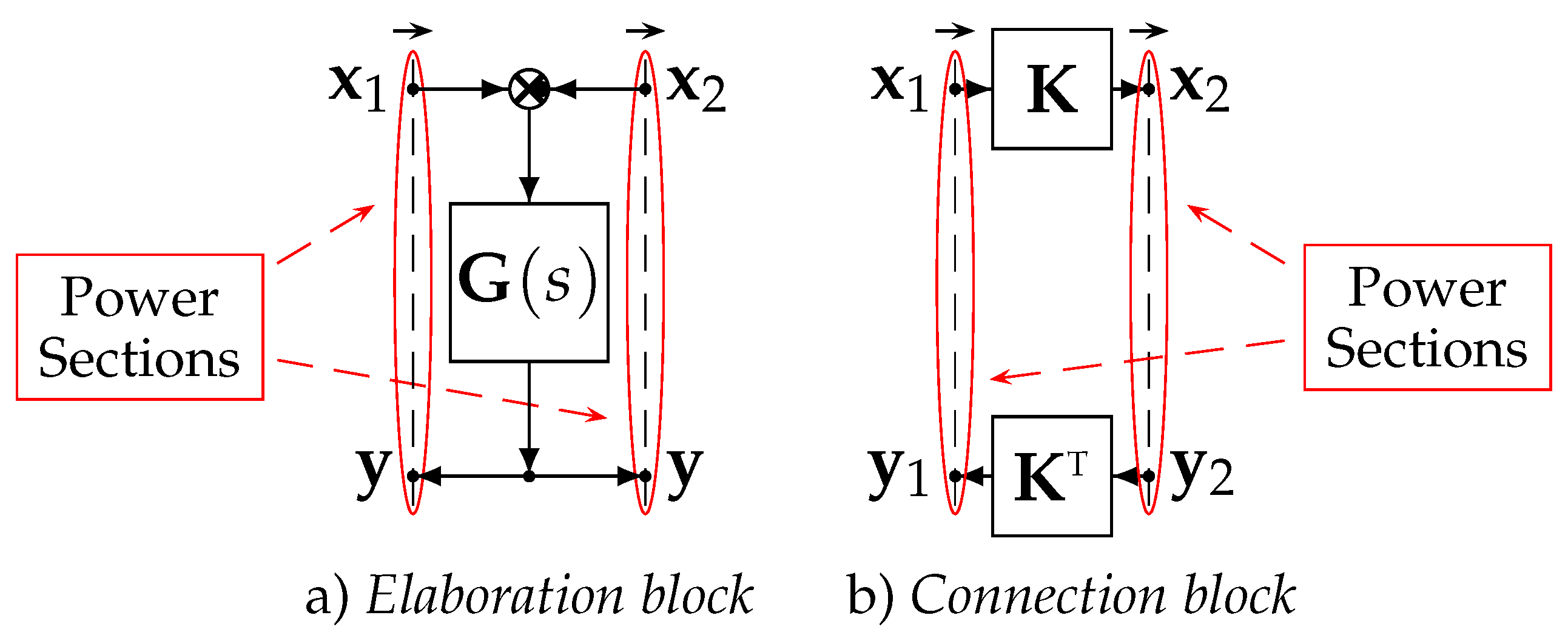
2. The POG Modeling Technique
- across elements, having a flow variable as input and an across variable as output;
- flow elements, having an across variable as input and a flow variable as output.
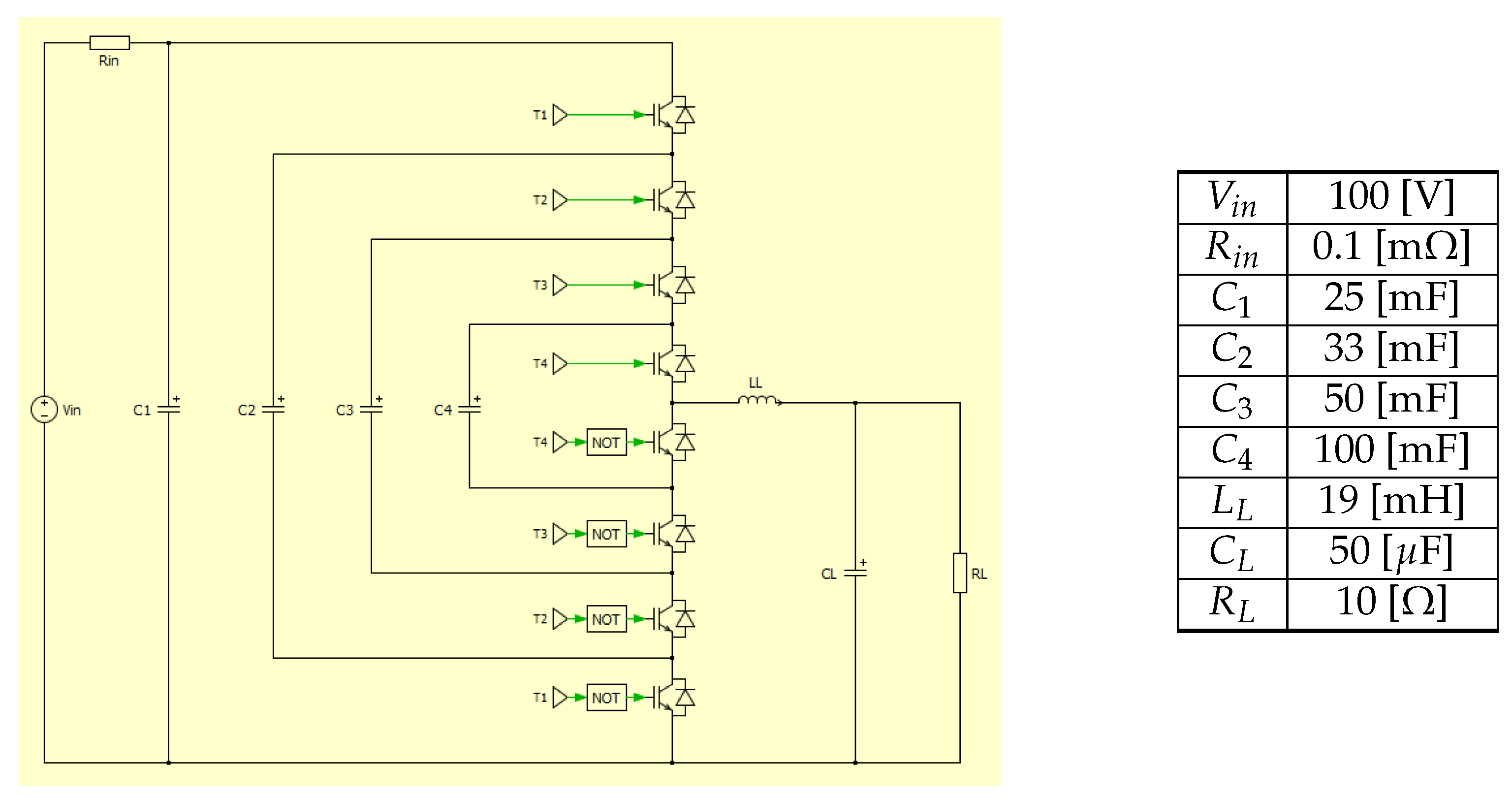
3. Modeling of the n-Dimensional Multilevel Flying-Capacitor Converter
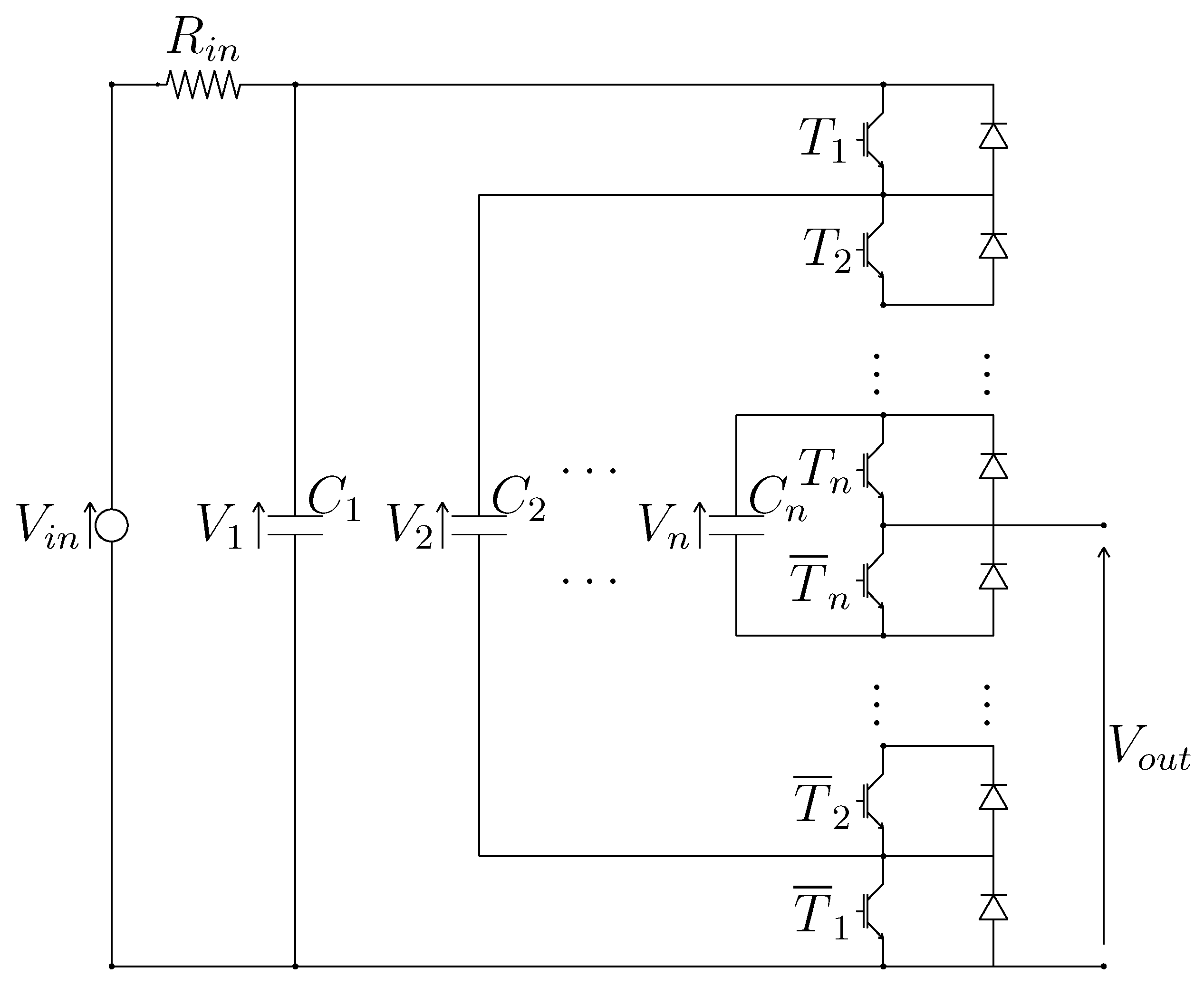
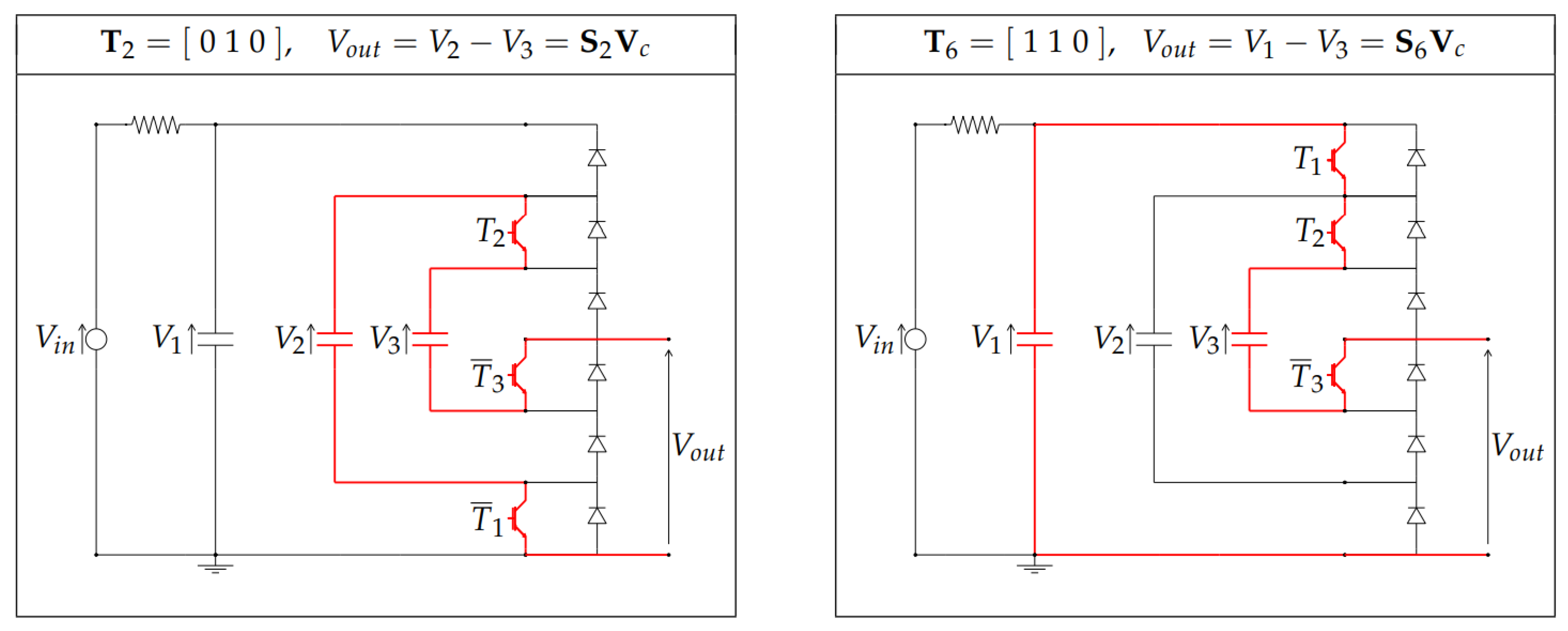
3.1. Physical System and Configuration Vectors
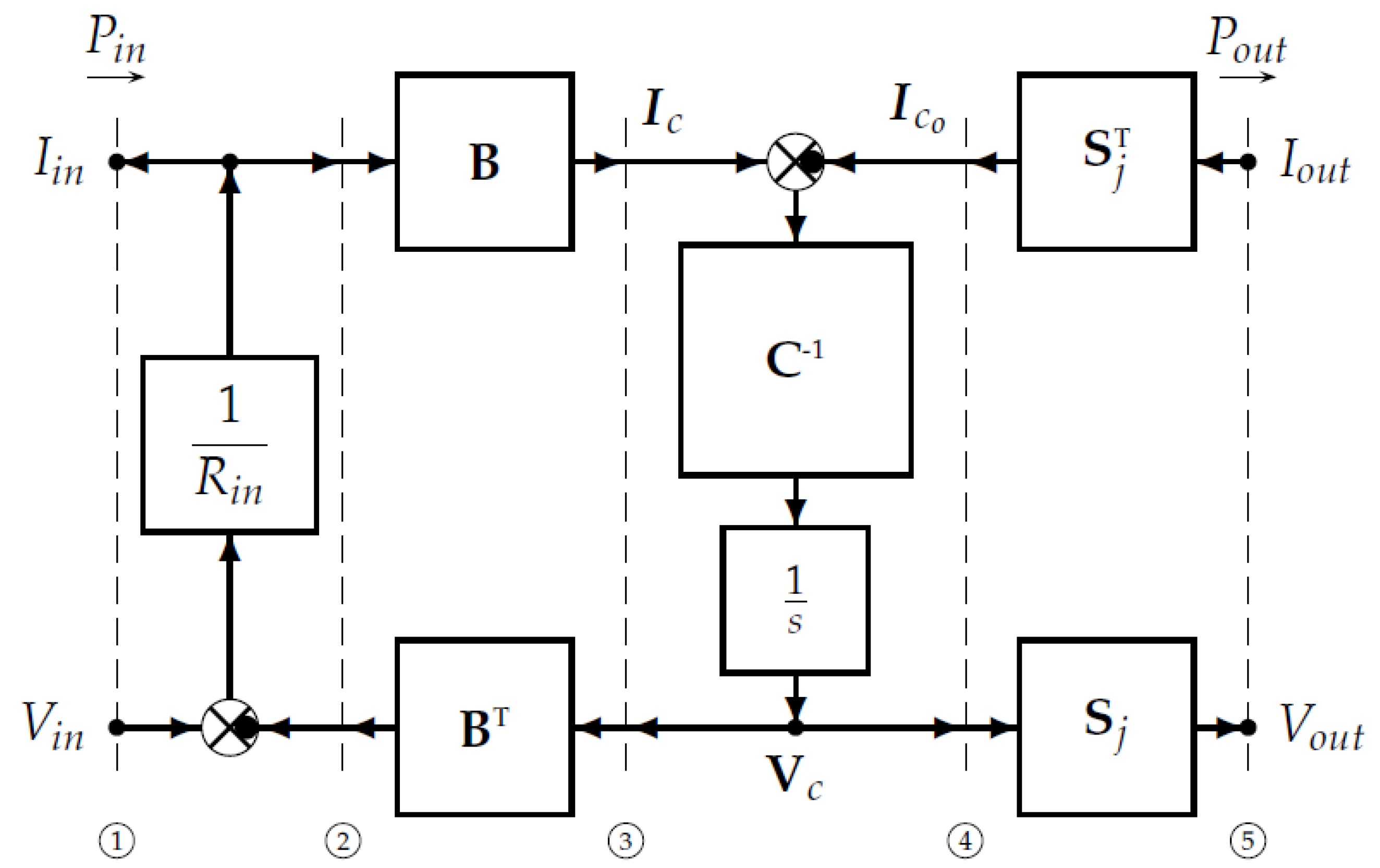
3.2. Dynamic Model of the Multilevel Flying-Capacitor Converter
- The energy matrix groups together the dynamic physical parameters for , namely the system capacitors.
- The power matrix and the input matrix contain the static physical parameter , which is the system input resistance.
- The configuration vector contains the control signals that directly determine how the output current is going to charge/discharge the capacitors through and, at the same time, how the output voltage is going to be generated from the capacitors voltages through (2).
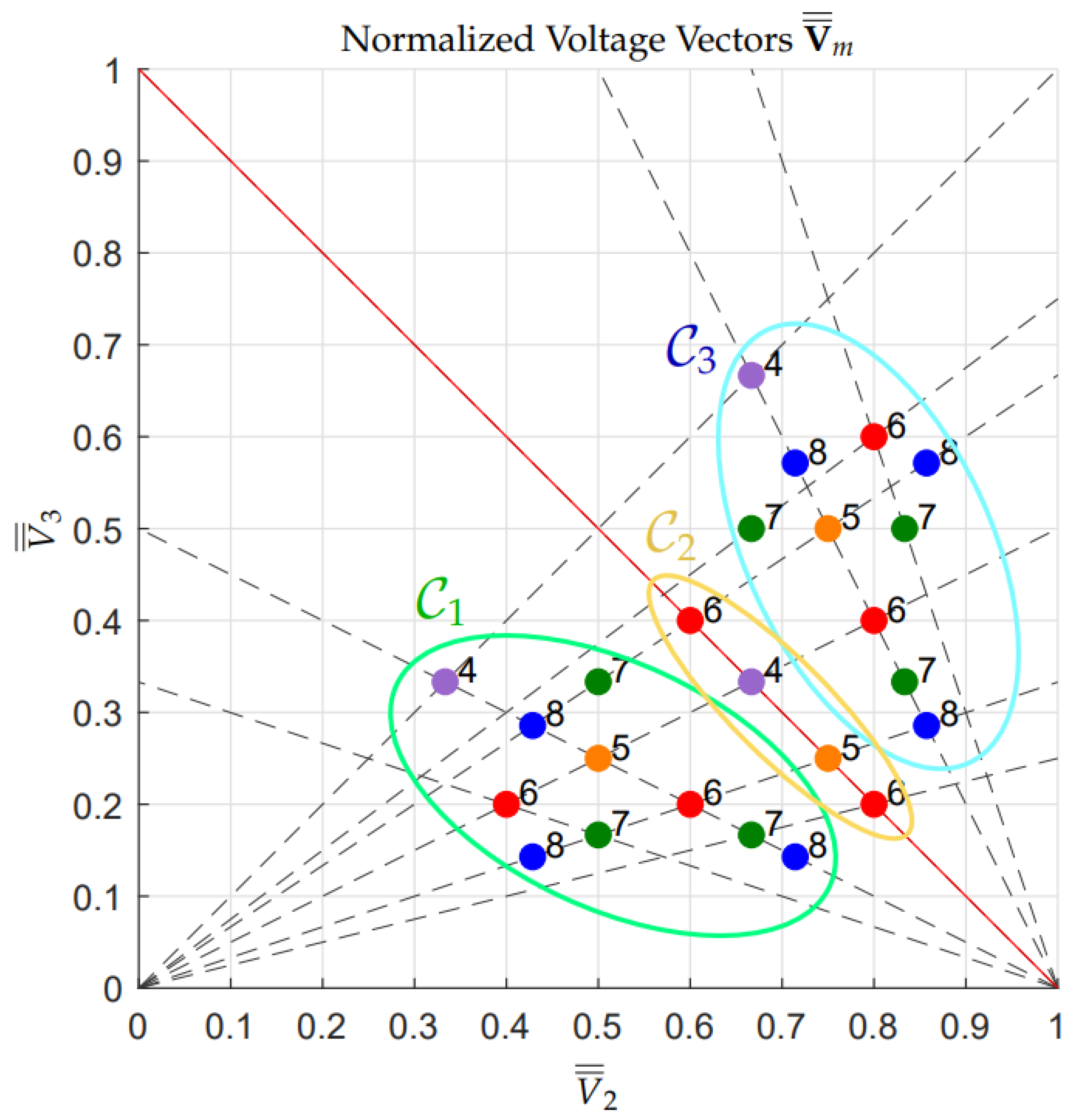
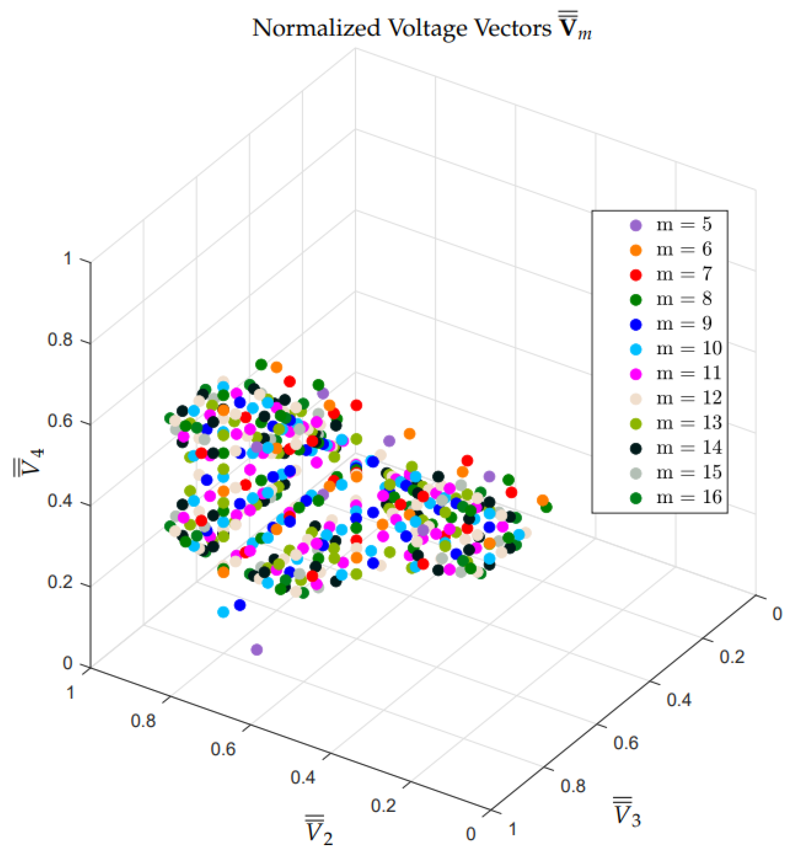
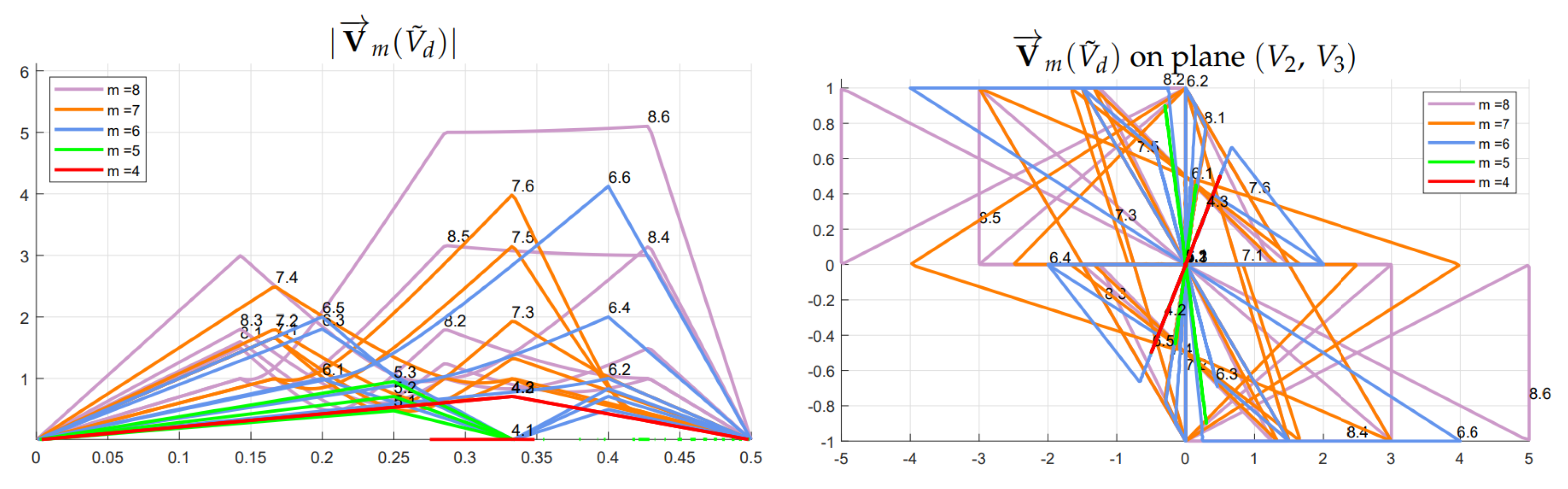
3.3. Calculation of All the Configuration Voltage Vectors
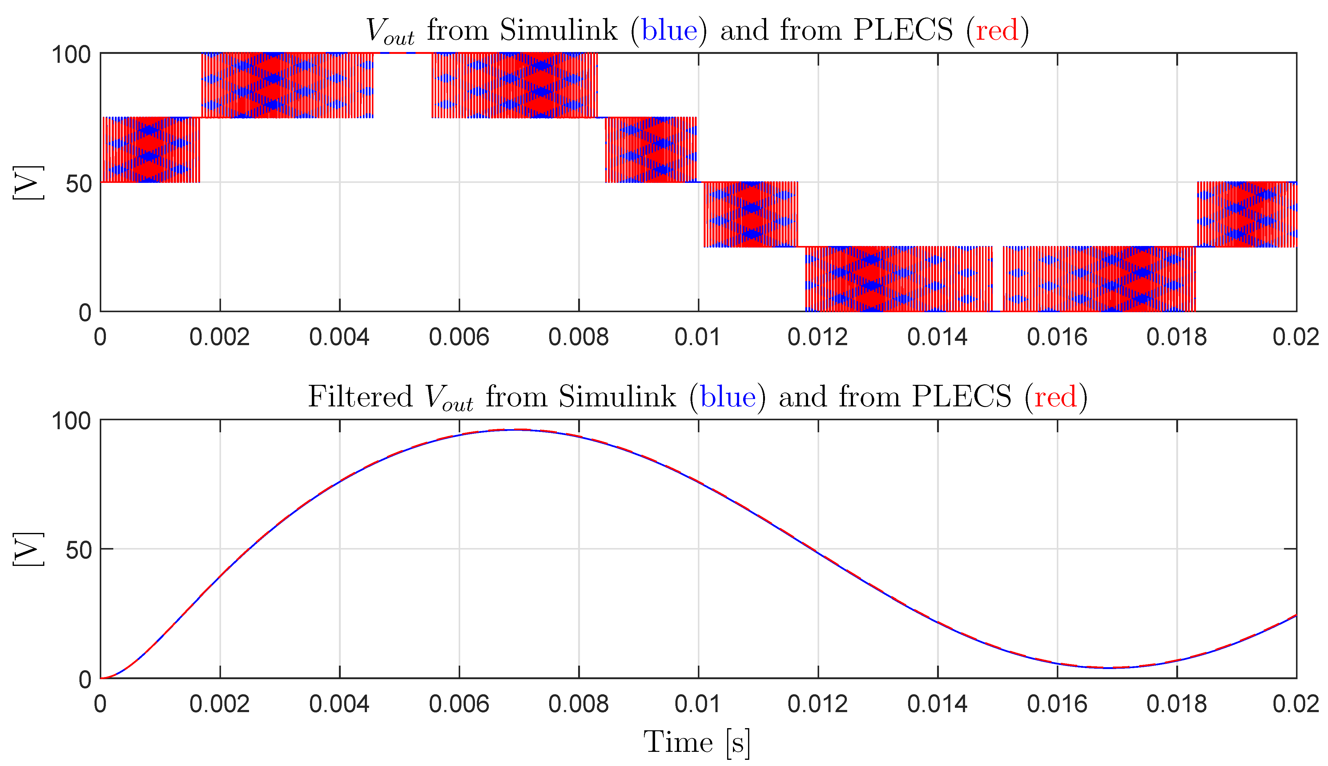
3.4. Model Verification
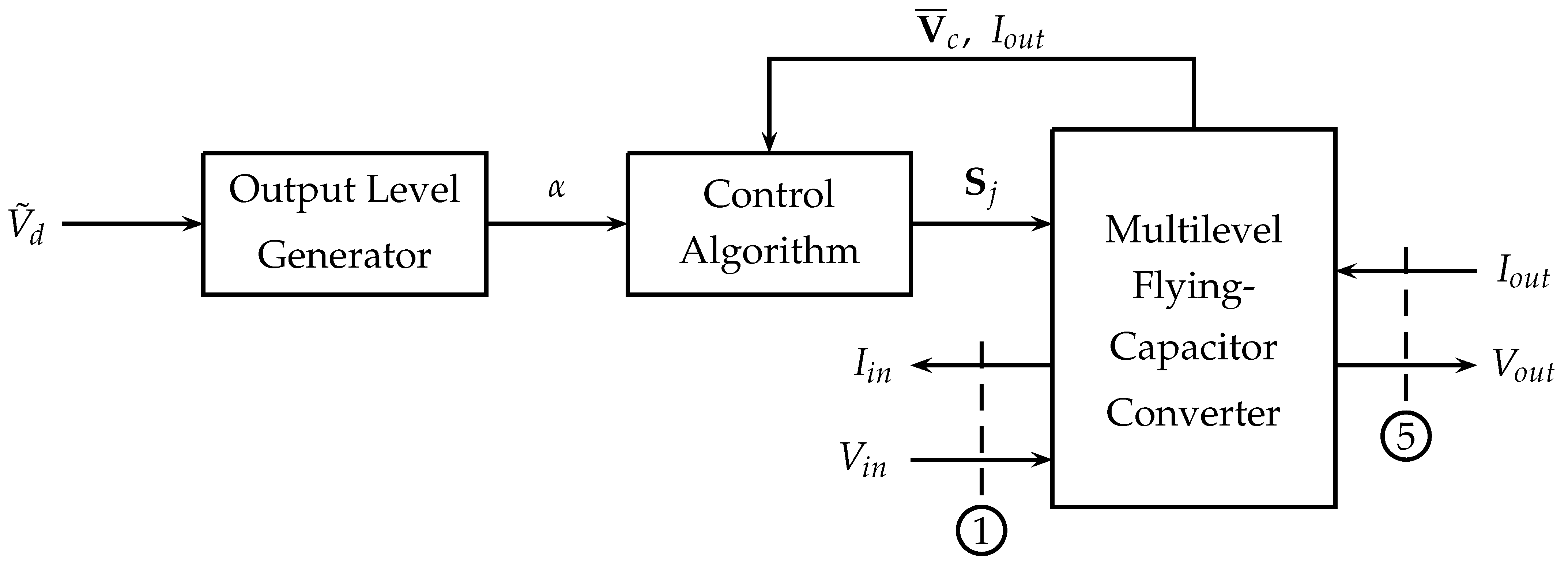
4. Control of the Multilevel Flying-Capacitor Converter
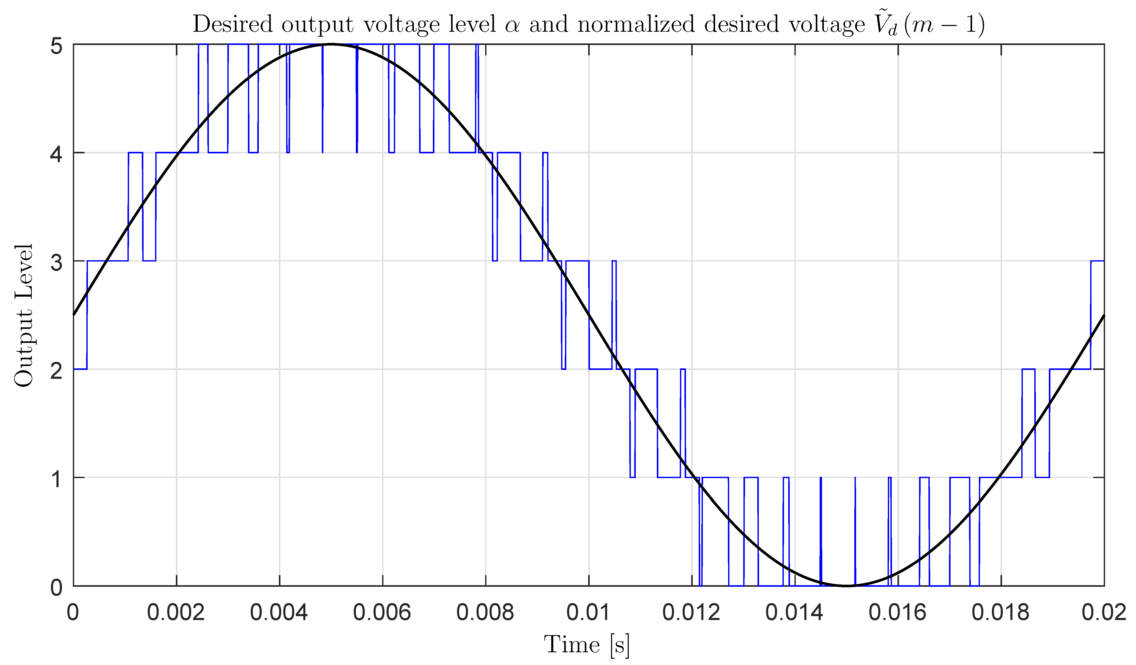
4.1. Minimum Distance Control
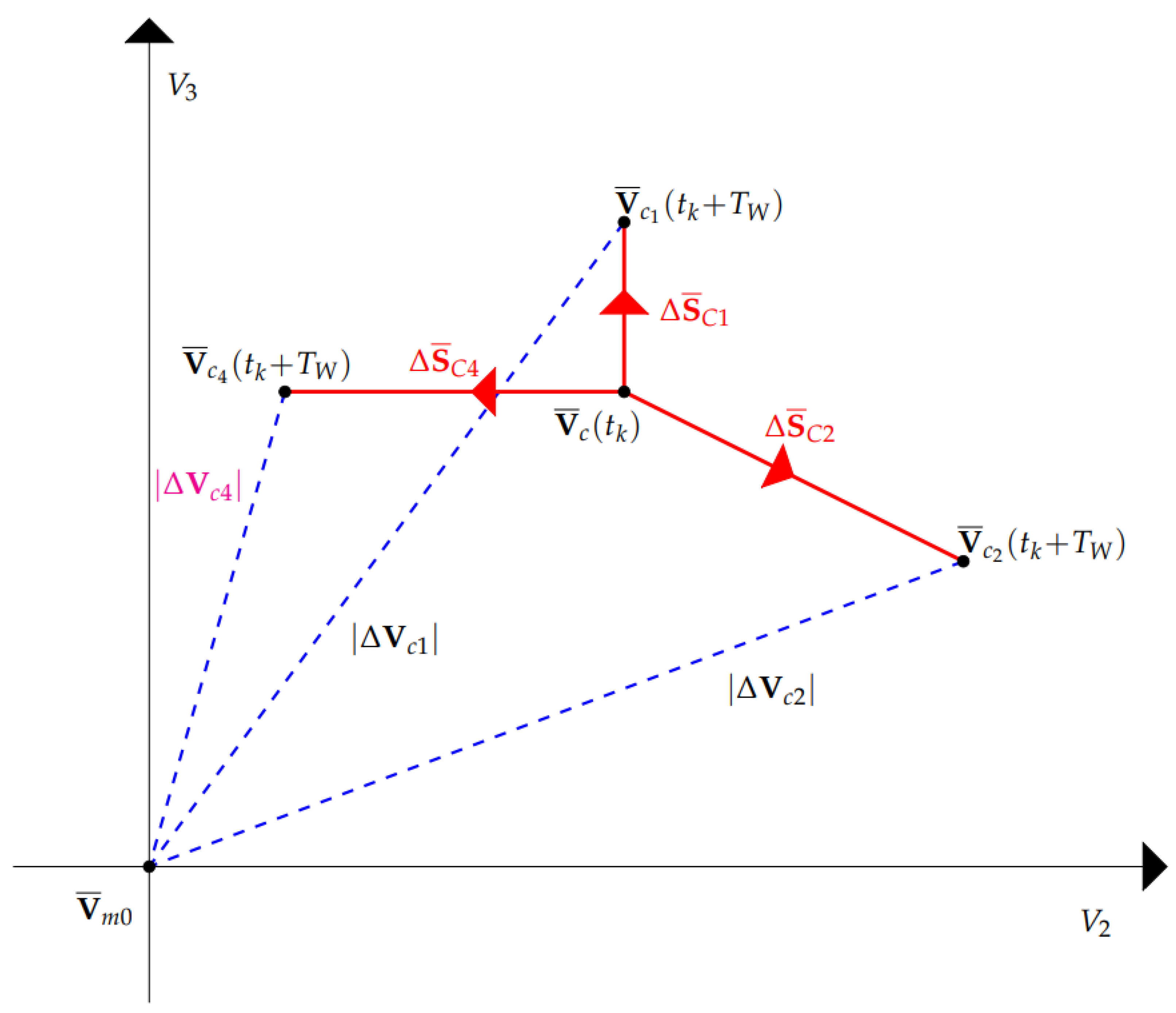
- At instant , read the value of the reduced voltage vector ;
- For any , compute the new position of the reduced voltage vector at instant , which is due to the application of the configuration vector :where is the value of the output current at instant and is the time for which the configuration vector is applied.
- For any , compute the following distance vectors:between points and the desired reduced Voltage Vector .
- At instant , apply the configuration vector , with , for which the norm of vectors is minimized:
4.2. Basic Configurations
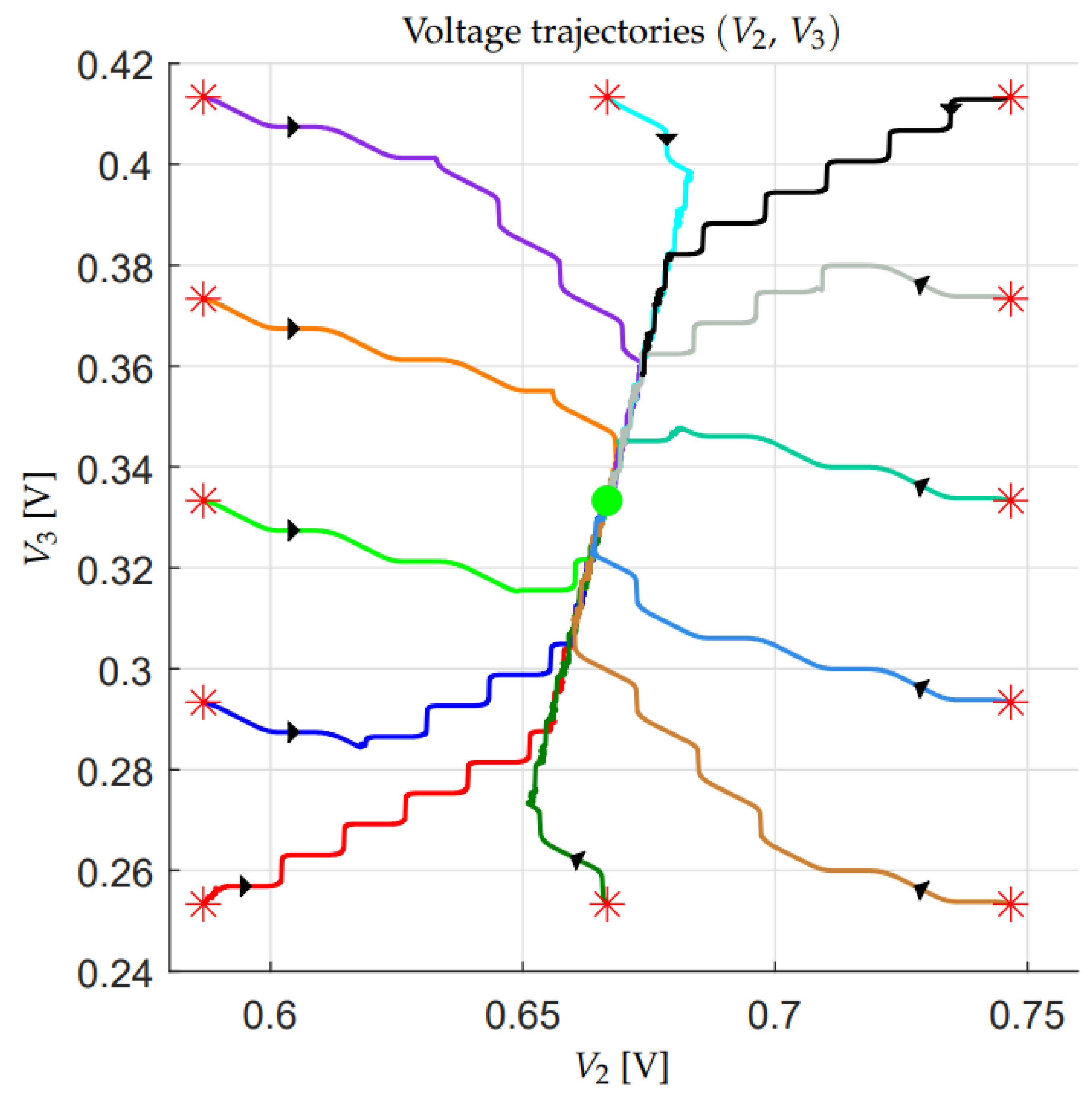
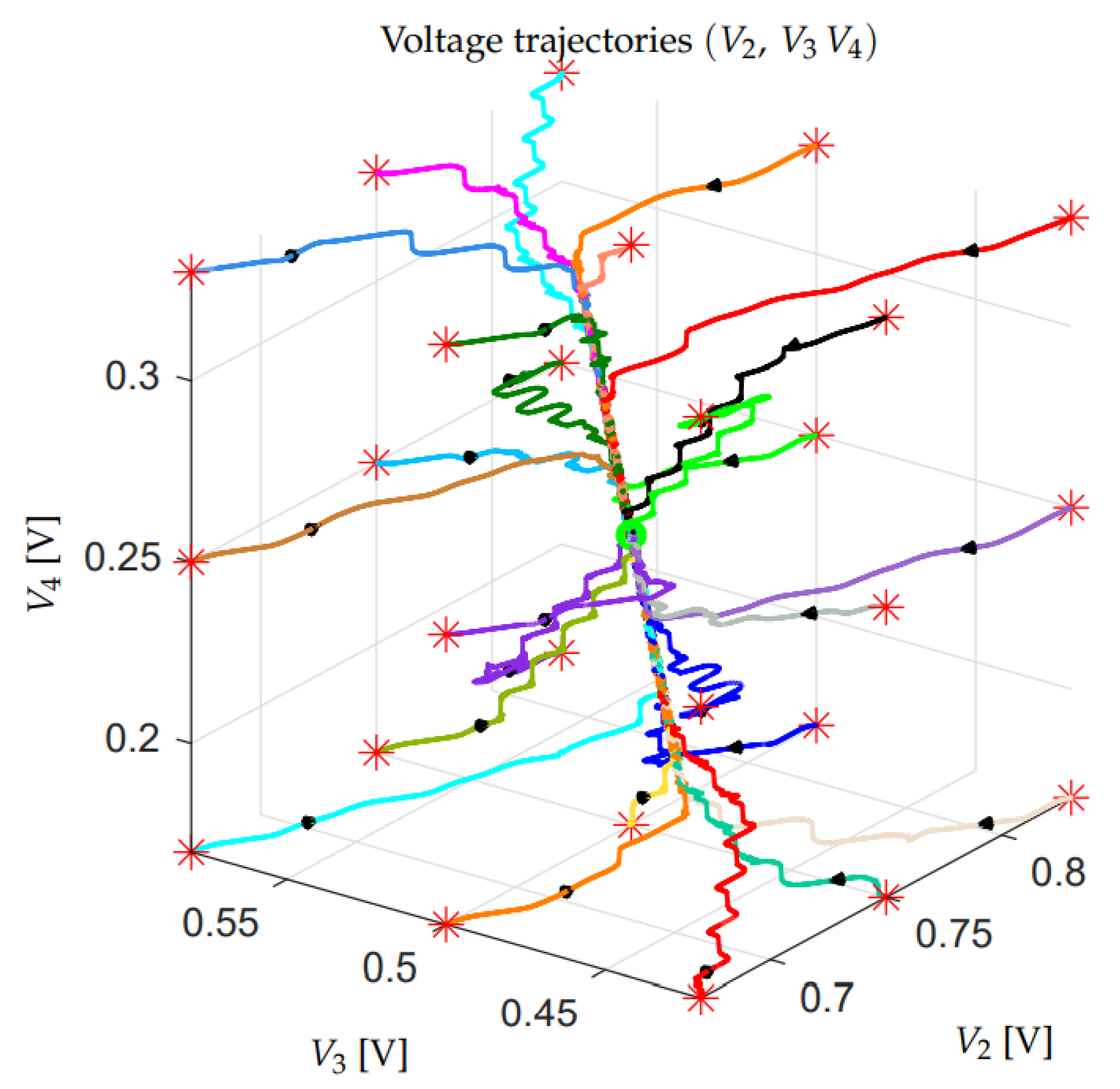
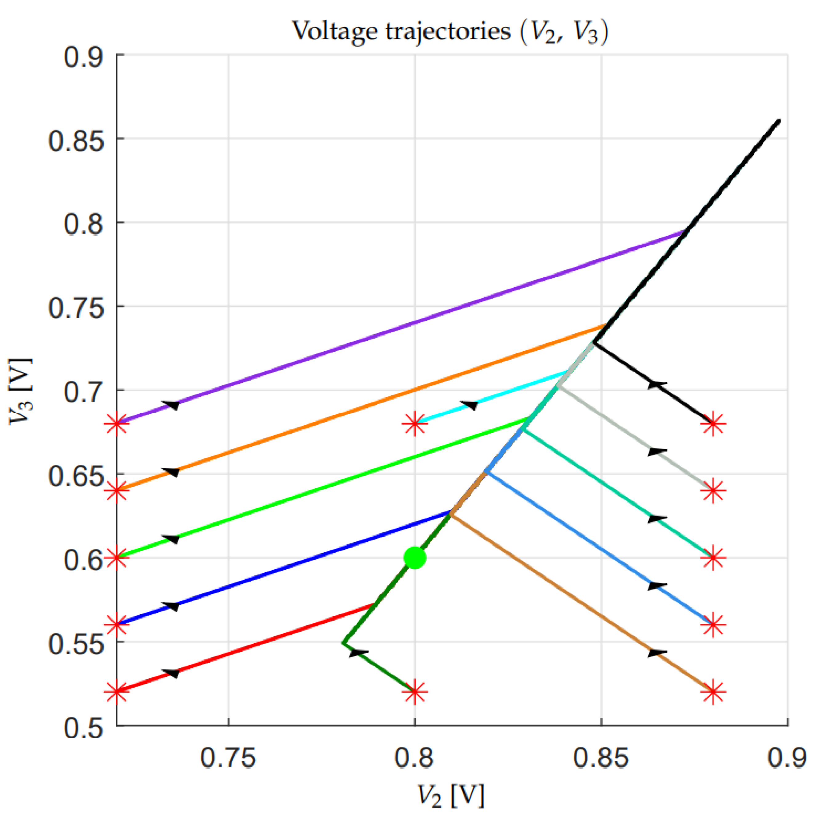
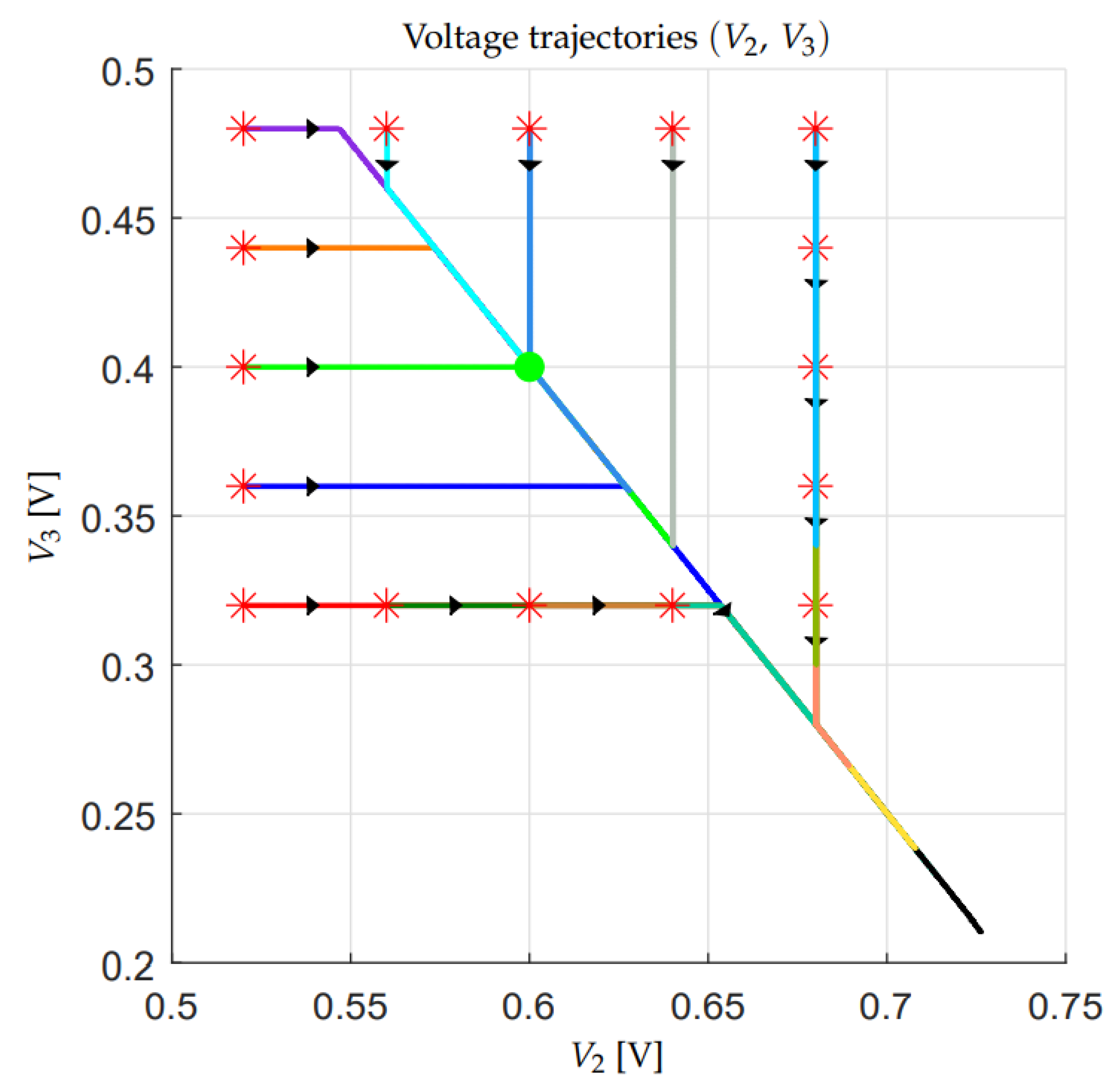
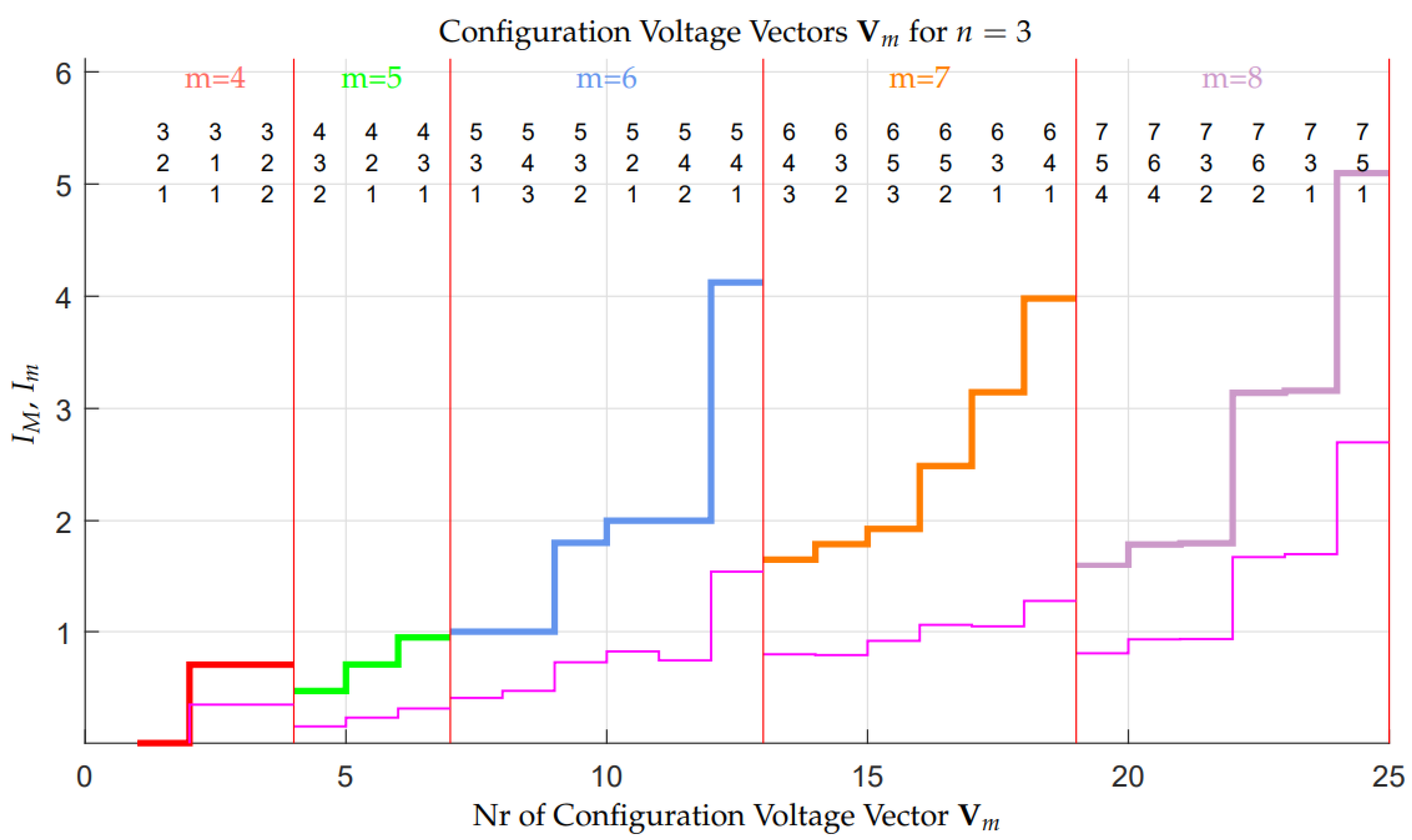
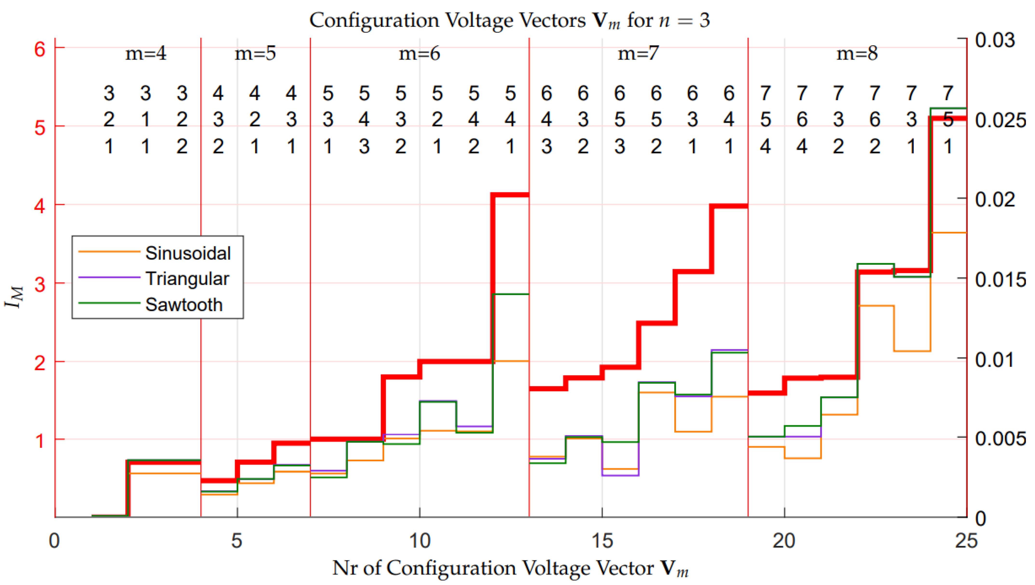
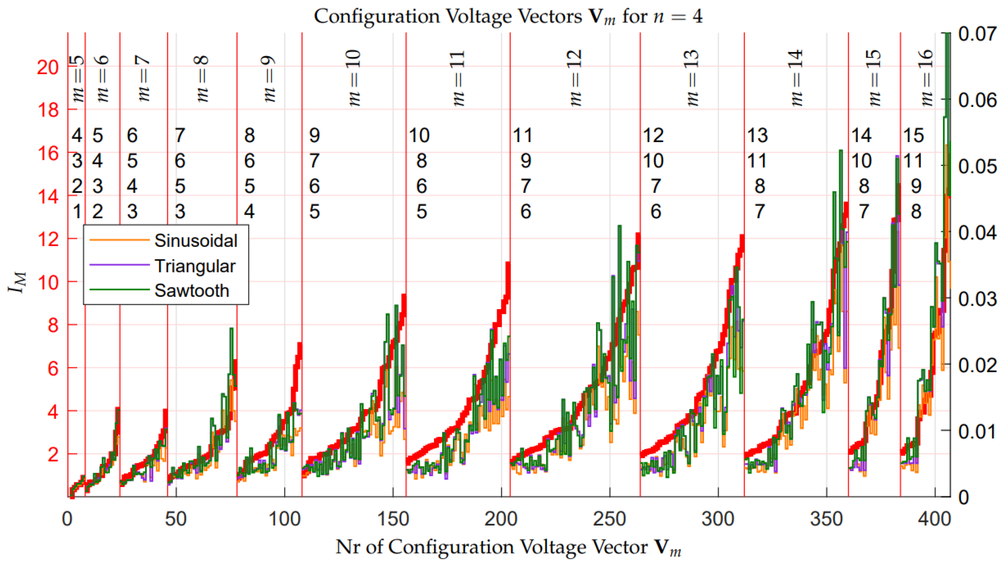
4.3. Robustness Assessment of the Configuration Voltage Vectors
- Given the Configuration Voltage Vectors and the value of the last n-th capacitor , let us choose the values of the remaining capacitors , , …, , as follows:namely, each capacitor is chosen inversely proportional to the components of vector .
- The Minimum Distance Algorithm that is given in Section 4.1 can be rewritten in an equivalent form by using the following Matlab-like function “”, which must be called providing :
| function Compute set defined in (23); Compute vectors defined in (22) using (29); for Compute as follows, see (25): ; end Find for which the norm of vectors is minimized, as in (26); Set ; Set ; |
| ; | % Function normalized with respect to |
| ; | % Function normalized with respect to time |
| ; | % Function normalized with respect to |
| for | % of variable |
| % of variable | |
| ; | % Upper adjacent level |
| % Lower adjacent level | |
| % Duty cycle of the upper level | |
| % Zero initial condition | |
| for | % Repeat times |
| % Time interval of the upper level | |
| % Upper level Minimum Distance Algorithm | |
| % Time interval of the lower level | |
| % Lower level Minimum Distance Algorithm | |
| end | |
| % Function is defined in point | |
| end |
4.3.1. Minimum Distance Control: Stability Issues in Extended Operation
- (A)
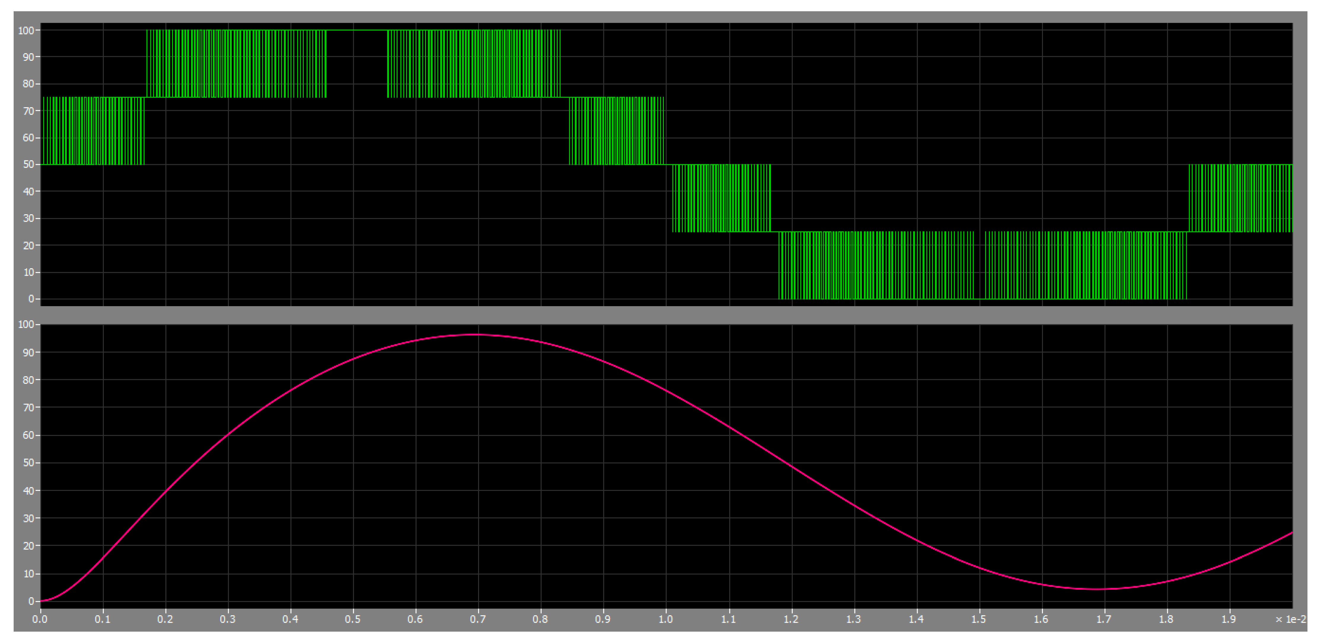
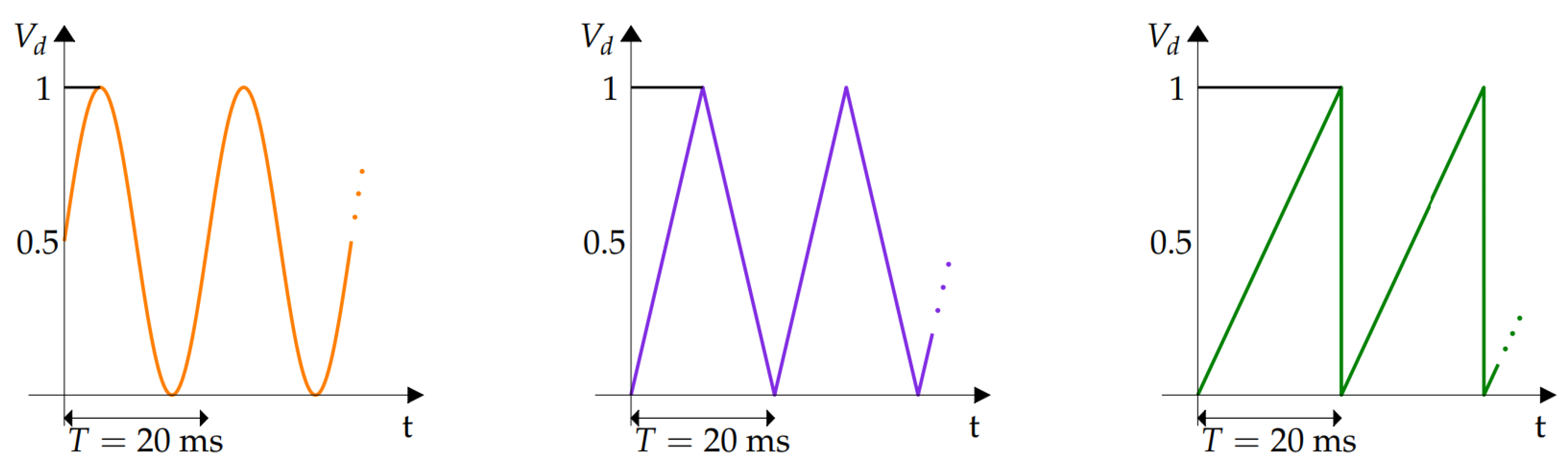
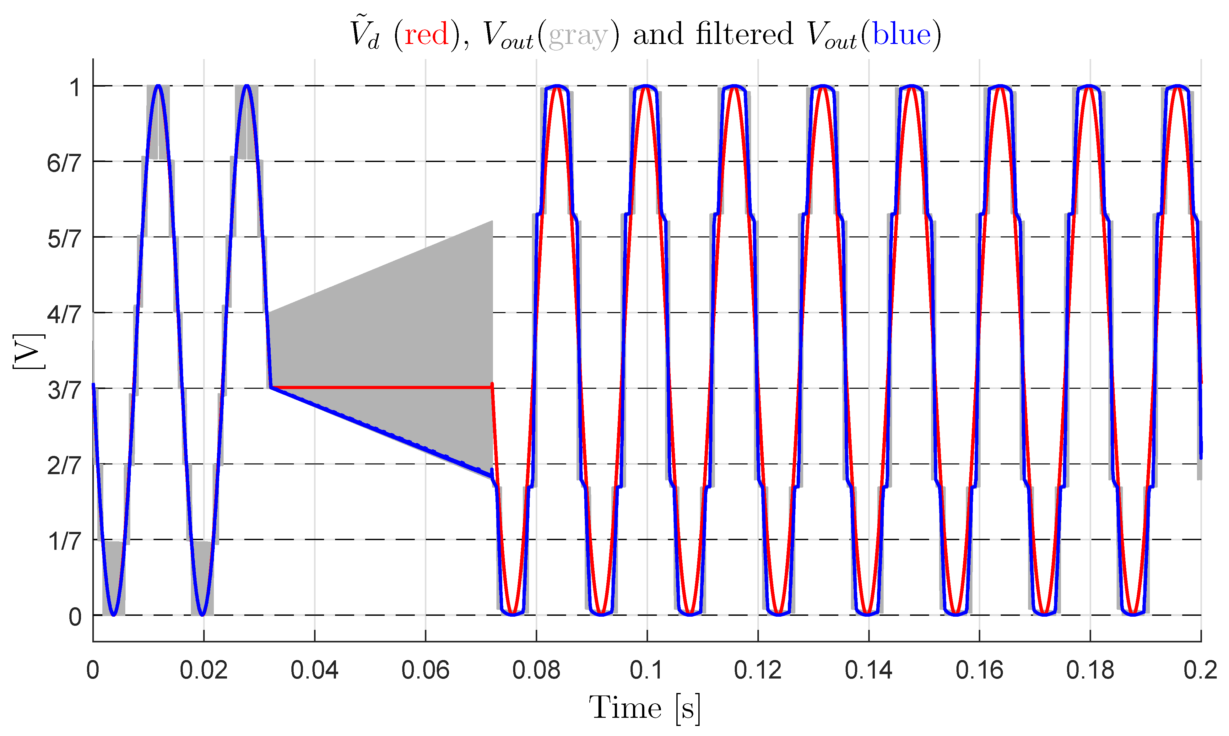
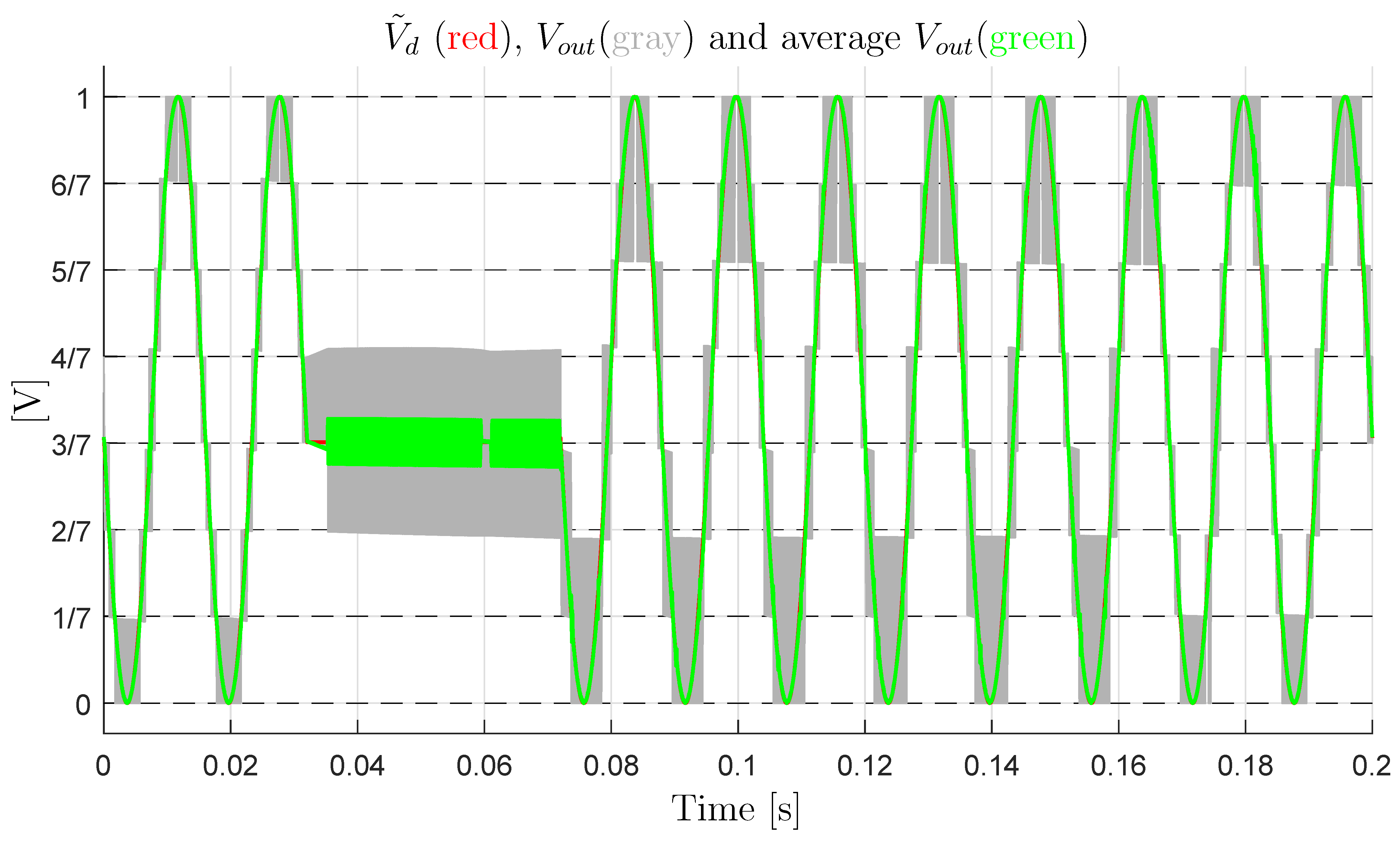
- Let us consider the case of a constant output current A and a sinusoidal desired voltage with an average value that is equal to 0.5: . Furthermore, the voltage signal is supposed to remain constant at the value for a short time interval , where and . Figure 22 shows the simulation results. The red characteristic in Figure 22 is the desired signal , the gray characteristic is the output switching signal , whereas the blue characteristic is the average value of the output signal . From the figure, it is evident that: (1) in the first part of the simulation, i.e., , the multilevel converter works correctly, since the output switching levels are equally spaced and, thus, the output voltage error is very low; (2) during the second part of the simulation, i.e., , the values of the output switching levels change considerably with respect to the desired ones, and they are no longer equally spaced. Therefore, the average value of the output signal (blue characteristic) is no longer equal to the desired value (red characteristic); and, (3) in the third part of the simulation, i.e., , the multilevel converter no longer works correctly, since the output signals (the gray and blue characteristics) are no longer equal to the desired one (the red characteristic). This is due to the fact that the trajectories of the reduced voltage vector have diverged from the desired value because of the constant voltage . Moreover, the Minimum Distance algorithm is not able to force the reduced voltage vector to move back towards the desired voltage vector after divergence has occurred.
- (B)
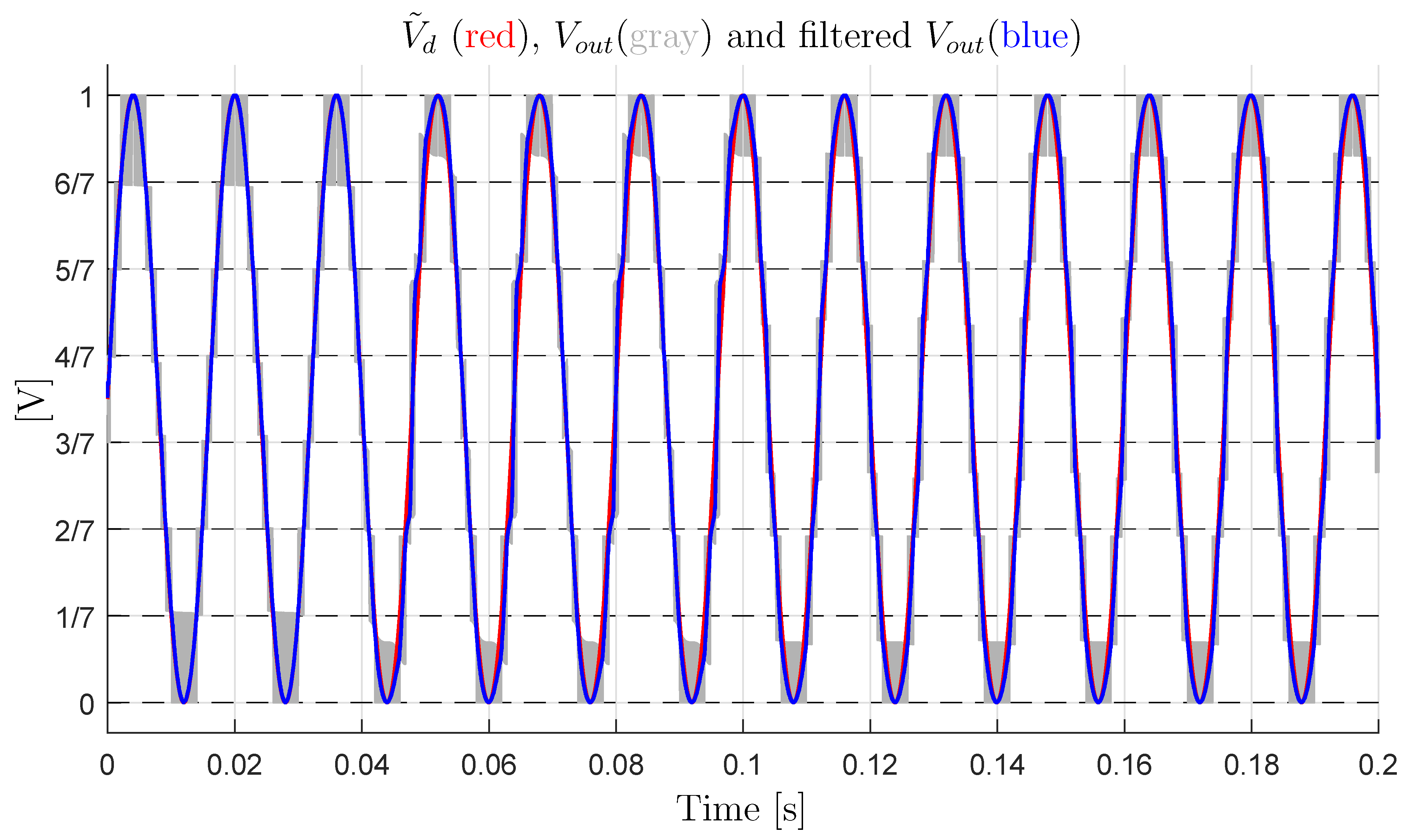
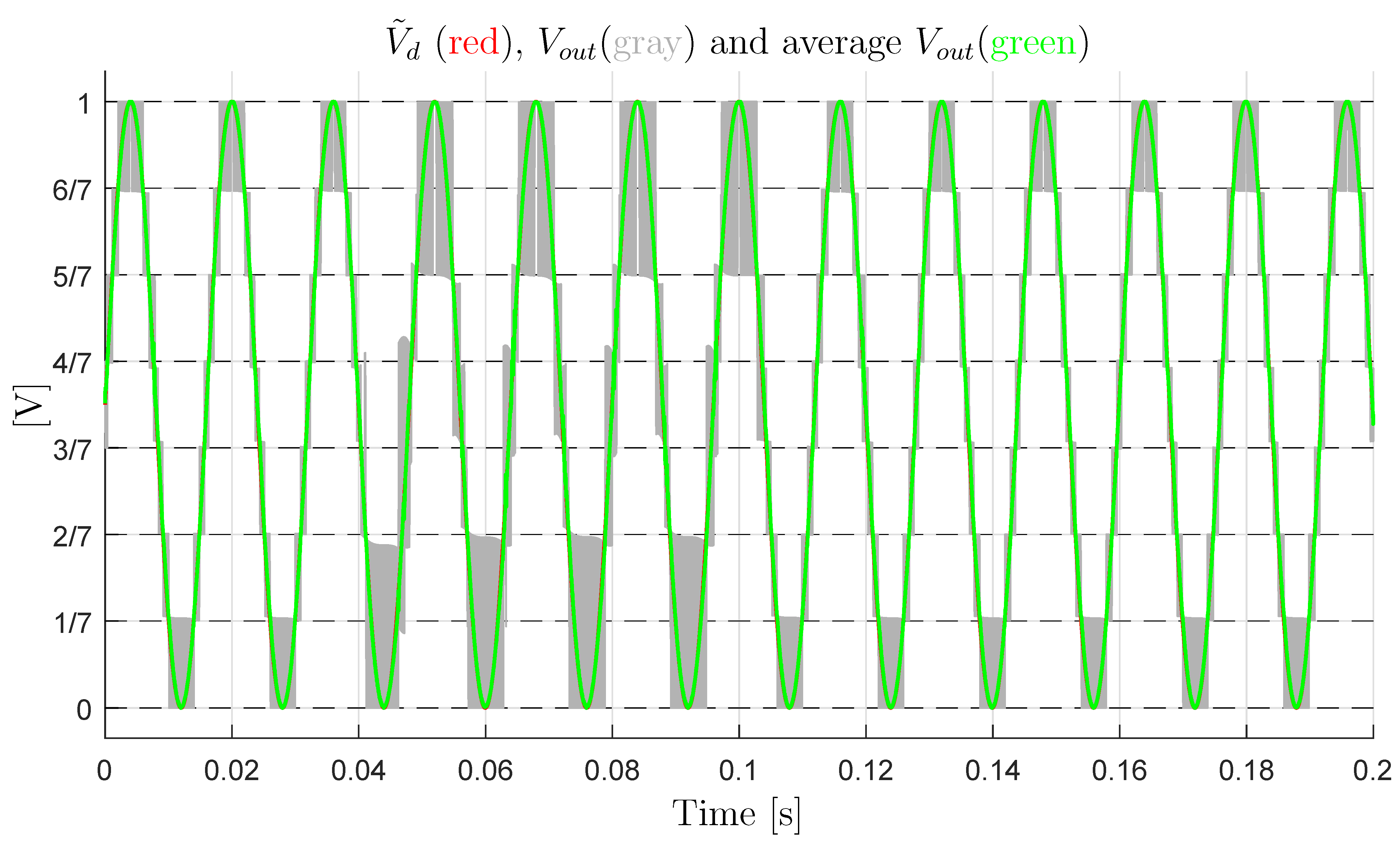
- Let us consider the case of a sinusoidal desired voltage with an average value that is equal to 0.5: . The load current is supposed to be constant and equal to for . Next, a sudden load change causing a current step is supposed to occur, causing to jump from to for . The load operating condition giving is supposed to be reestablished for . Figure 23 shows the simulation results. The characteristics color notation is the same as the one adopted in Figure 22. From Figure 23, it is evident that: (1) in the first part of the simulation, i.e., , the multilevel converter works correctly, since the output switching levels are equally spaced, which means that the output voltage error is very low; (2) for , the values of the output switching levels change with respect to the desired ones, and they are no longer equally spaced; and, (3) for , the output voltage levels remain unequally spaced, due to the divergence of the trajectories of the reduced voltage vector from the desired value caused by the sudden load change. Moreover, the Minimum Distance algorithm is not able to force the reduced voltage vector to move back towards the desired voltage vector after the divergence has occurred.
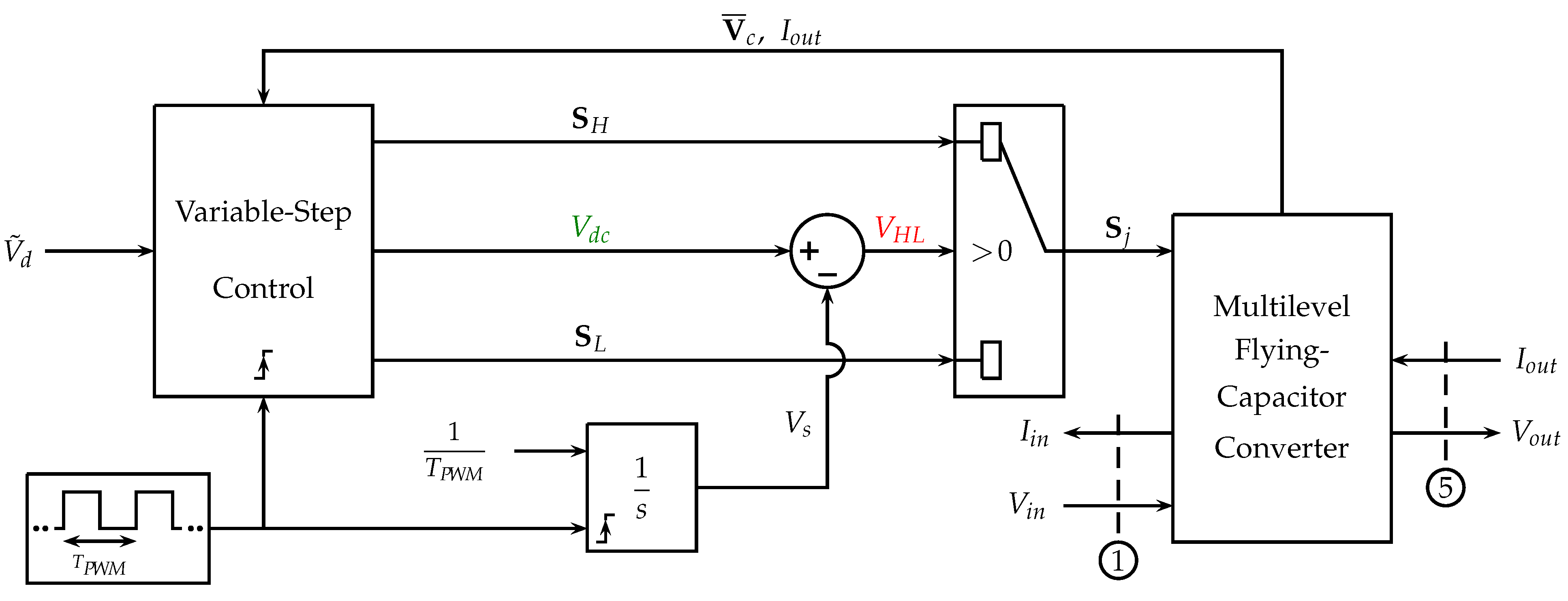
4.4. Variable-Step Control of the Multilevel Flying-Capacitor Converter
- (a)
- a square wave signal having period acting as a clock, which activates the Variable-Step Control and resets the integrator to the zero initial condition when the rising edge occurs;
- (b)
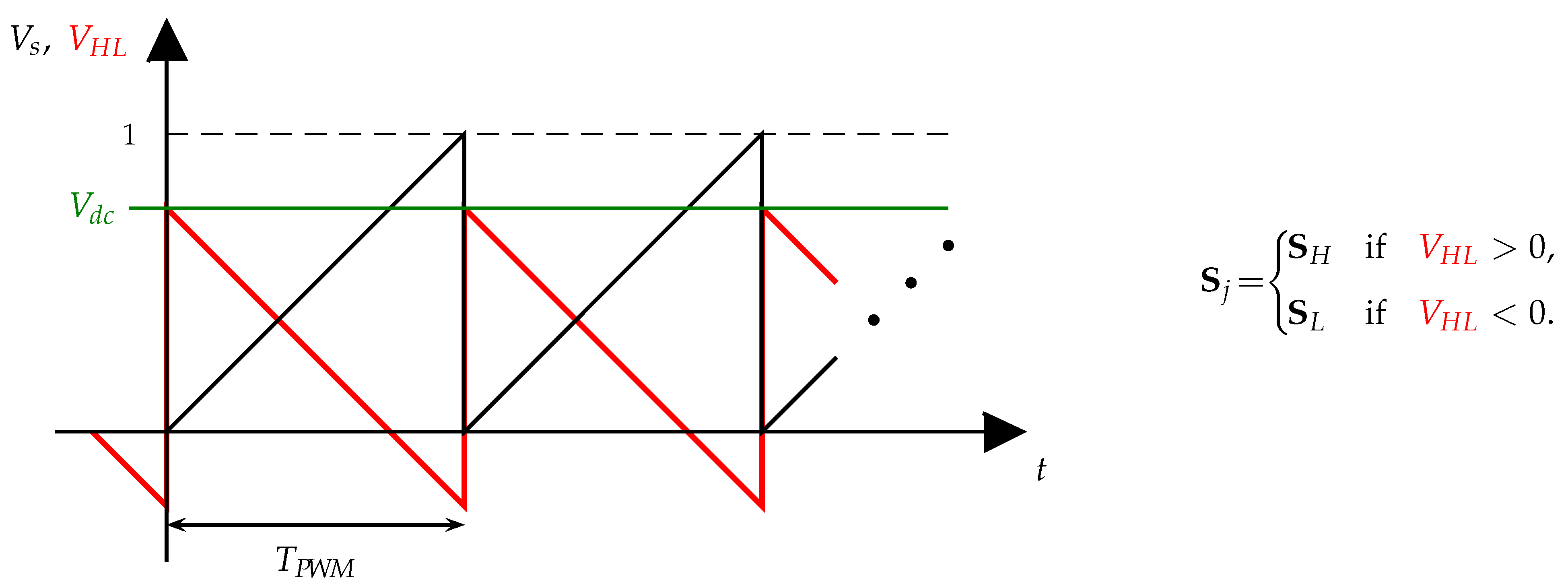
- an integrator with a constant input and a reset signal that is timed by the square clock. The output of the integrator is a sawtooth signal which ranges from 0 to 1 within a time interval , where is the reset time instant, see the black line in Figure 25;
- (c)
- the voltage that is provided by the Variable-Step Control block, defining the duty cycle of the high level of the PWM signal, namely the time interval , see the green line in Figure 25;
- (d)
- the value of the signal determines the output of the selector and, thus, the configuration vector , which is going to be applied to the multilevel converter during the next time interval: for a time interval and for a time interval ;
- (e)
- at each activation time, the Variable-Step Control reads the input signal and generates three output signals: , and . Using these signals, the Variable-Step Algorithm can decide the duty cycle and the two levels and of the next PWM period;
- (f)
- let denote the voltage corresponding to configuration vector and denote the voltage corresponding to configuration vector . The duty cycle of the next PWM period, that is the ratio between the duration of the higher level and the duration of the PWM period , can be computed, as follows:Using (30), the duty cycle always guarantees that the average value of the PWM output voltage in the next period is equal to the desired value .
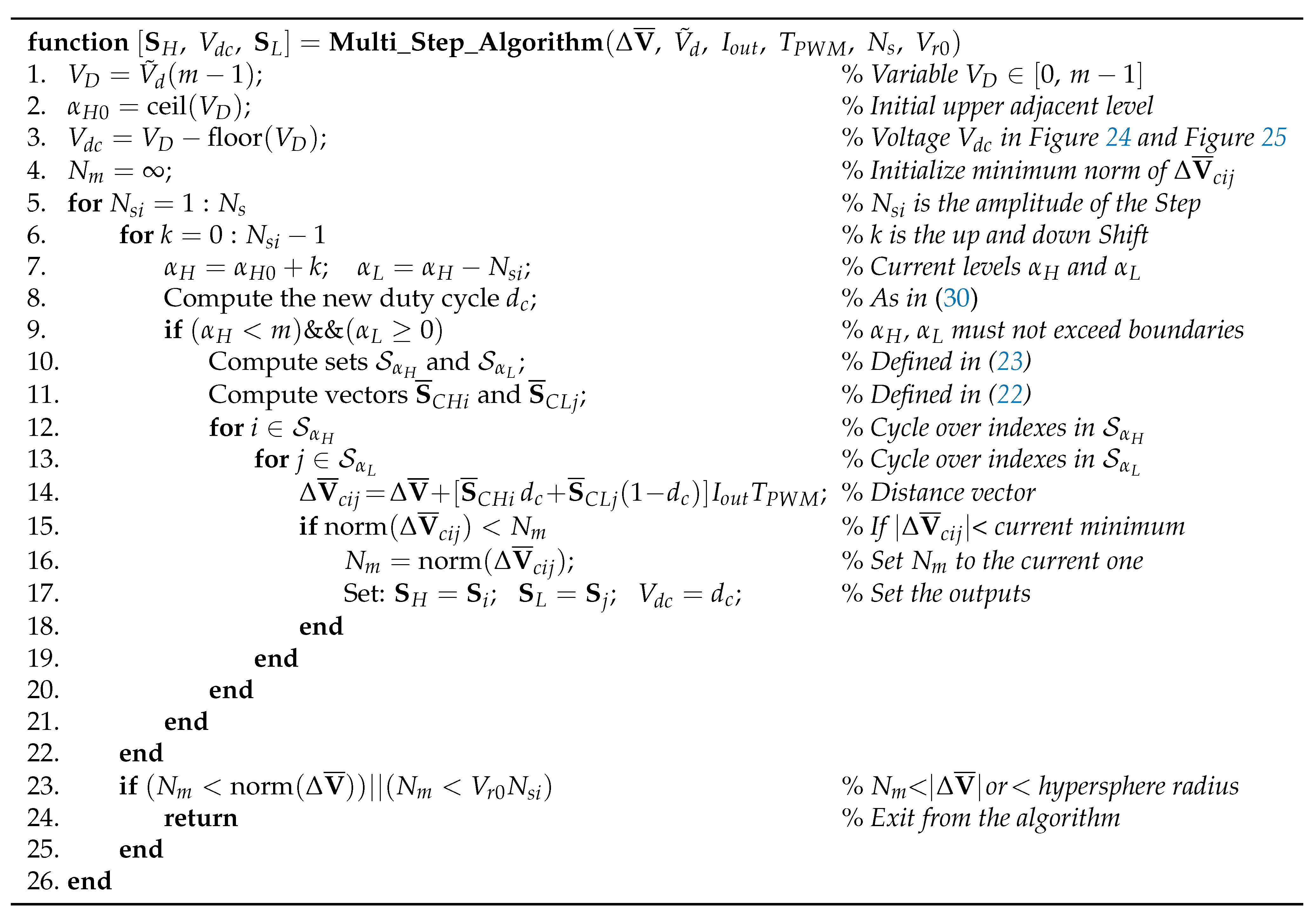
- At each activation time , the “Multi_Step_Algorithm” computes the two configuration vectors , and the duty cycle to be applied in the following PWM time interval : configuration will be applied in the first part of the PWM period when , while configuration will be applied in the second part of the PWM period when , see Figure 25.
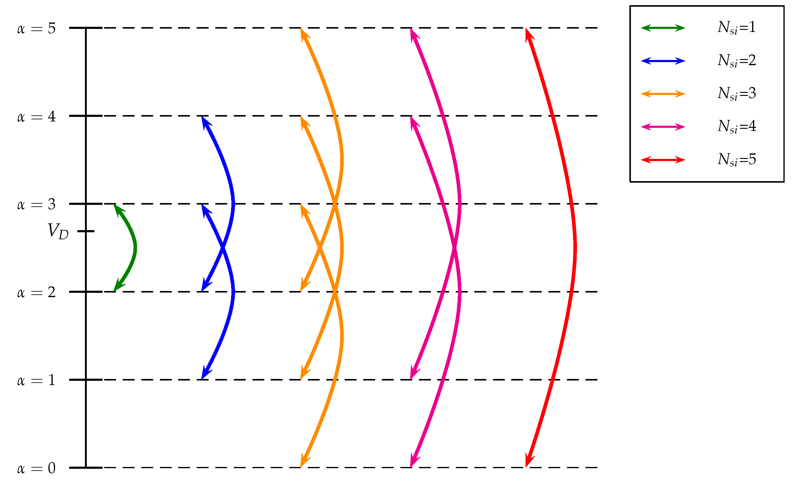
- The input defines the maximum amplitude of the Step to be used in the algorithm, which is the maximum level-to-level distance. The for cycle at line 5 in Figure 26 defines the current value of the amplitude of the Step, i.e., the current level-to-level distance. The for cycle at line 6 defines the current value k of the up and down shift to be considered for the current amplitude of the Step.
- At lines 7 and 8, the current values of the upper level , the lower level , and the duty cycle are computed. If the current values of and are admissible, see condition at line 9, then the sets and of the admissible configuration vectors and and the corresponding vectors and are computed at lines 10 and 11.
- The two for cycles at lines 12 and 13 are used to compute the distance vector for each possible combination of the configuration vectors and belonging to the two sets and . At line 14, the distance vector is computed starting from the initial condition and adding the two terms and , due to the application of the configuration vectors and in the first part and in the second part of the PWM period , respectively.
- If the norm of the distance vector is smaller than the current minimum norm , see line 15, then the algorithm updates the value of parameter , see line 16, and it sets the values of the output variables , and equal to the values , and of the current solution, see line 17.
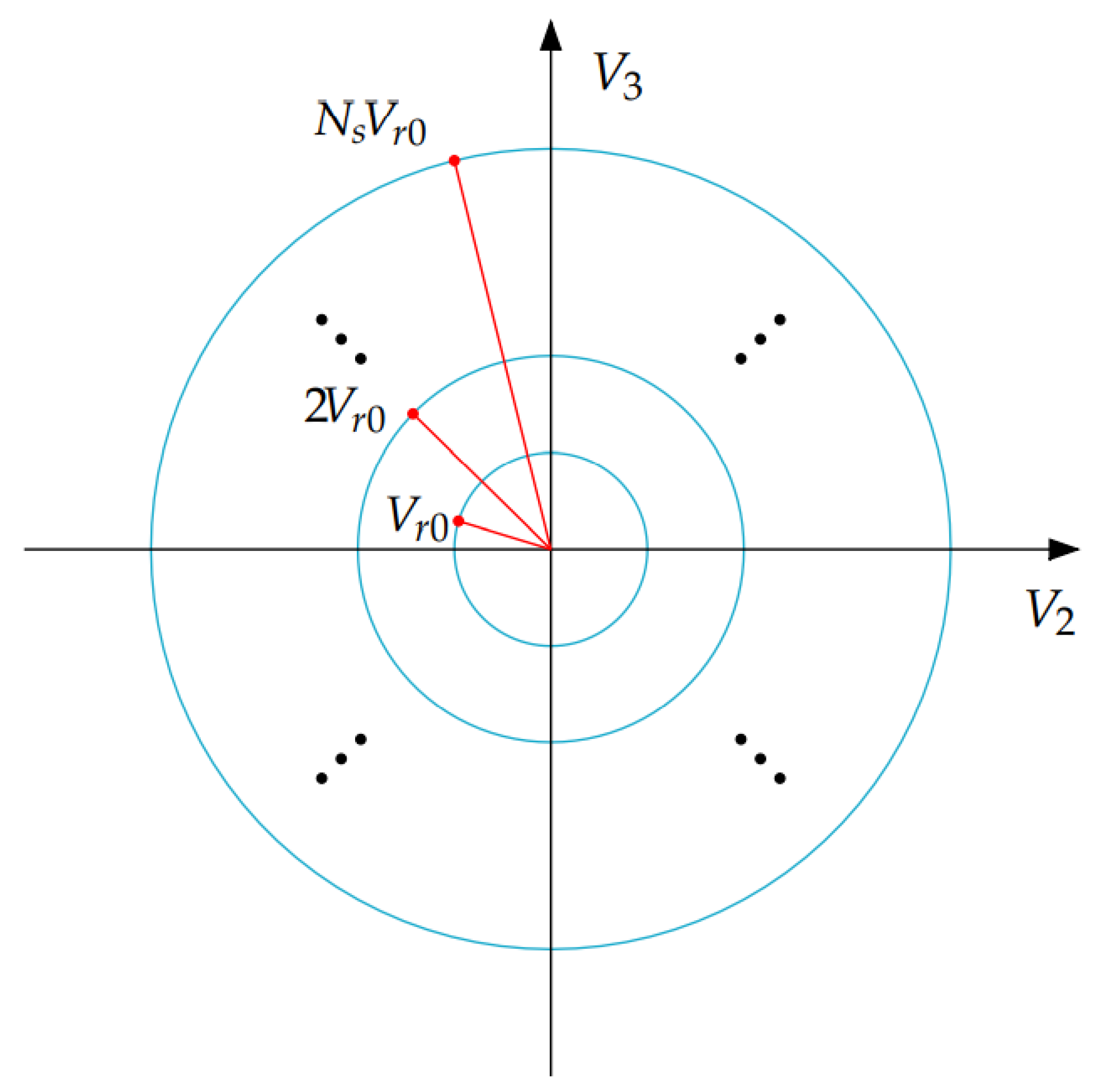
- The “Multi_Step_Algorithm” ends its minimum distance vector search, see line 24, when one of the conditions at line 23 is verified, or when the maximum level-to-level distance has been achieved. At line 23, the algorithm exits the search if the current minimum distance is lower than the initial one, or if is lower than radius , where is the input basic radius and is the current level-to-level distance. Radius represents the varying radius of an hypersphere in the -dimensional space. Figure 27 shows the resulting circumferences with varying radius for the case .
- The “Multi_Step_Algorithm” introduces and uses the new concept of “variable level-to-level distance”. This concept means that the algorithm can choose a higher level and a lower level that are not adjacent, see line 7 of the algorithm. The current level-to-level distance is denoted by variable . The new duty cycle associated with the two levels and , computed in line 8, guarantees that the average value of the PWM output voltage in the next PWM period will be equal to the desired value .
- The ability to change the level-to-level distance allows the “Multi_Step_Algorithm” to keep the reduced voltage vector in the vicinity of the desired voltage vector even in extended operation and in presence of some particularly unfavorable operating conditions, such as normalized desired voltage having an average value different from 0.5.
- If the unfavorable conditions persist, the algorithm can enlarge the level-to-level distance up to its upper boundary . This enlargement increases the number of the configuration vectors that the algorithm can use to keep vector in the vicinity of the desired vector , and to maintain the correct functioning of the multilevel converter. Furthermore, when the unfavorable conditions no longer occur, the “Multi_Step_Algorithm” has the ability to force the converter to go back to work as a normal multilevel converter switching between adjacent levels only, i.e., with a current level-to-level distance equal to one.
- The example reported in Figure 28 shows all the possible combinations of levels and that can be obtained when , and the desired voltage is in between levels “2” and “3”.


4.4.1. Variable-Step Control: Solution of the Stability Issues in Extended Operation
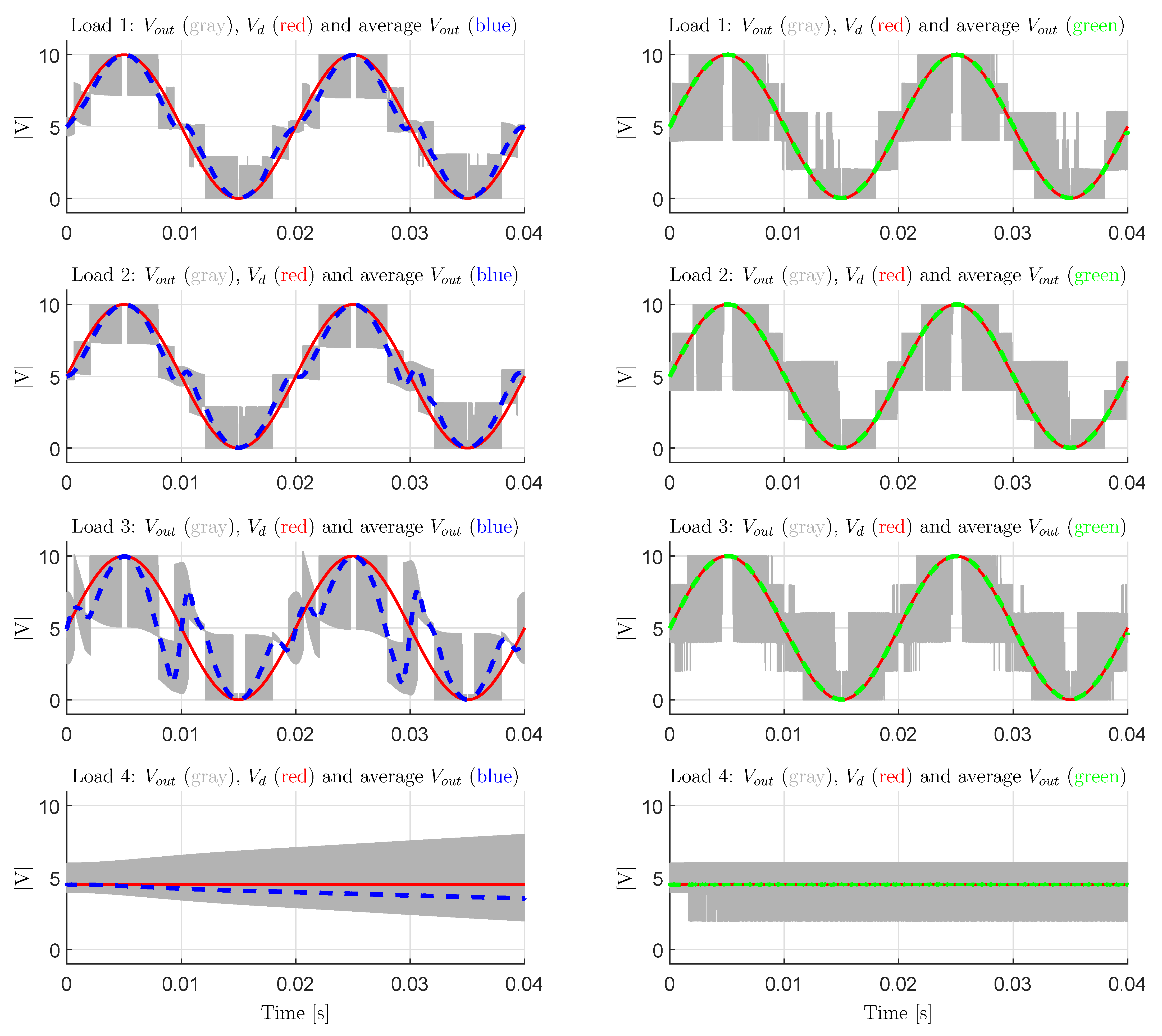
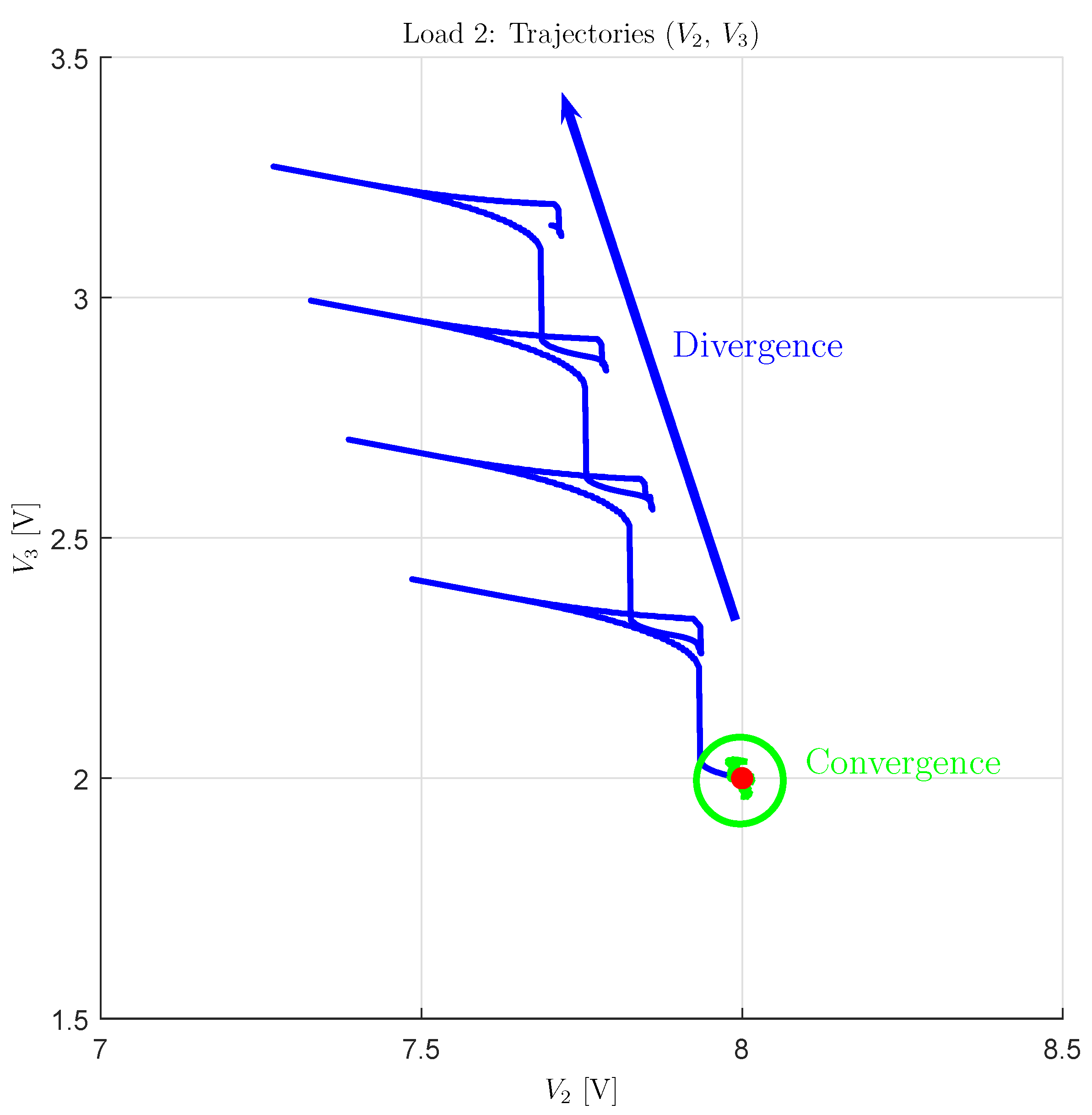
5. Converter Testing with Dynamic Loads
6. Conclusions
- the Power-Oriented Graphs modeling technique has been exploited to derive the system dynamic model of the n-dimensional converter, generating a POG model that can be directly implemented in Matlab/Simulink by employing standard Simulink libraries;
- a procedure for computing all the possible voltage vector configurations providing equally spaced levels of the output voltage has been given;
- the robustness assessment of the converter operating in extended mode when using a Minimum Distance Control has been performed;
- a Divergence Index has been introduced, which can be used as a metric for properly ordering the different Configuration Voltage Vectors on the basis of their voltage balancing capability in extended operation;
- a new Variable-Step Control algorithm has been proposed, allowing for the safe extended operation of the converter even under particularly destabilizing operating conditions, such as a constant desired output voltage or a sudden load change.
Author Contributions
Funding
Data Availability Statement
Conflicts of Interest
References
- Zanasi, R.; Cuoghi, S. Model of Soft-Switching Converter and Power Control of Grid-Connected Photovoltaic Systems. In Proceedings of the IECON Annual Conference of the IEEE Industrial Electronics Society, Melbourne, VIC, Australia, 7–11 November 2011. [Google Scholar] [CrossRef]
- Wu, H.; Mu, T.; Ge, H.; Xing, Y. Full-Range Soft-Switching-Isolated Buck-Boost Converters with Integrated Interleaved Boost Converter and Phase-Shifted Control. IEEE Trans. Power Electron. 2016, 31, 987–999. [Google Scholar] [CrossRef]
- Azer, P.; Emadi, A. Generalized State Space Average Model for Multi-Phase Interleaved Buck, Boost and Buck-Boost DC-DC Converters: Transient, Steady-State and Switching Dynamics. IEEE Access 2020, 8, 77735–77745. [Google Scholar] [CrossRef]
- Zanasi, R.; Cuoghi, S. Model of Soft-Switching Converter and Power Control for Smart Grid Applications. In Proceedings of the IEEE PES Innovative Smart Grid Technologies, Perth, WA, Australia, 13–16 November 2011. [Google Scholar] [CrossRef]
- Al-Badi, A.H.; Ahshan, R.; Hosseinzadeh, N.; Ghorbani, R.; Hossain, E. Survey of Smart Grid Concepts and Technological Demonstrations Worldwide Emphasizing on the Oman Perspective. Appl. Syst. Innov. 2020, 3, 5. [Google Scholar] [CrossRef]
- Wu, B.; Narimani, M. High-Power Converters and AC Drives; Wiley-IEEE Press: Hoboken, NJ, USA, 2017. [Google Scholar]
- Quraan, M.; Tricoli, P.; D’Arco, S.; Piegari, L. Efficiency Assessment of Modular Multilevel Converters for Battery Electric Vehicles. IEEE Trans. Power Electron. 2017, 35, 2041–2051. [Google Scholar] [CrossRef]
- Rodrìguez, J.; Lai, J.-S.; Peng, F.Z. Multilevel Inverters: A Survey of Topologies, Controls, and Applications. IEEE Trans. Ind. Electron. 2002, 49, 724–738. [Google Scholar] [CrossRef]
- Rodrìguez Bernet, J.S.; Wu, B.; Pontt, J.O.; Kouro, S. Multilevel Voltage-Source-Converter Topologies for Industrial Medium-Voltage Drives. IEEE Trans. Ind. Electron. 2017, 54, 2930–2945. [Google Scholar] [CrossRef]
- Saleh, S.A.; Al-Durra, A.; Ahshan, R. Ground Potentials in Transformerless Grid-Connected Multi-Level Power Electronic Converters. In Proceedings of the 56th Industrial and Commercial Power Systems Technical Conference (I&CPS), Las Vegas, NV, USA, 29 June–28 July 2020. [Google Scholar] [CrossRef]
- Saleh, S.; Al-Durra, A.; Ahshan, R. On the Ground Potentials and Grounding Circuits of Transformerless Grid-Connected Multilevel Power Electronic Converters. IEEE Trans. Ind. Appl. 2020, 56, 6286–6297. [Google Scholar] [CrossRef]
- Zanasi, R.; Cuoghi, S. Dynamic Models of Multilevel Converters by using the Power Oriented Graph Technique. In Proceedings of the International Symposium on Power Electronics, Electrical Drives, Automation and Motion, Sorrento, Italy, 20–22 June 2012. [Google Scholar] [CrossRef]
- Rodrìguez, J.; Franquelo, L.G.; Kouro, S.; Lèon, J.I.; Portillo, R.C.; Prats, M.A.M.; Pèrez, M.A. Multilevel Converters: An Enabling Technology for High-Power Applications. Proc. IEEE 2009, 97, 1786–1817. [Google Scholar] [CrossRef]
- Corzine, K.A.; Baker, J.R. Multilevel voltage-source duty-cycle modulation: Analysis and implementation. IEEE Trans. Ind. Electron. 2002, 49, 1009–1016. [Google Scholar] [CrossRef]
- Diaz, M.; Cardenas, R.; Ibaceta, E.; Mora, A.; Urrutia, M.; Espinoza, M.; Rojas, F.; Wheeler, P. An Overview of Modelling Techniques and Control Strategies for Modular Multilevel Matrix Converters. Energies 2020, 13, 4678. [Google Scholar] [CrossRef]
- Liu, M.; Li, Z.; Yang, X. A Universal Mathematical Model of Modular Multilevel Converter with Half-Bridge. Energies 2020, 13, 4464. [Google Scholar] [CrossRef]
- Zanasi, R. The Power-Oriented Graphs Technique: System modeling and basic properties. In Proceedings of the IEEE Vehicle Power and Propulsion Conference (VPPC), Lille, France, 1–3 September 2010. [Google Scholar] [CrossRef]
- Zanasi, R.; Geitner, G.H.; Bouscayrol, A.; Lhomme, W. Different energetic techniques for modelling traction drives. In Proceedings of the 9th Internation Conference on Modeling and Simulation of Electric Machines, Converters and Systems (ELECTRIMACS), Québec, QC, Canada, 8–11 June 2008. [Google Scholar]
- Zanasi, R. POG Modeler: The Web Power-Oriented Graphs Modeling Program. In Proceedings of the IFAC World Congress, Berlin, Germany, 11–17 July 2020. [Google Scholar]
- Brando, G.; Dannier, A.; Spina, I.; Tricoli, P. Integrated BMS-MMC Balancing Technique Highlighted by a Novel Space-Vector Based Approach for BEVs Application. Energies 2017, 10, 1628. [Google Scholar] [CrossRef]
- Liao, Y.; You, J.; Yang, J.; Wang, Z.; Jin, L. Disturbance-Observer-Based Model Predictive Control for Battery Energy Storage System Modular Multilevel Converters. Energies 2018, 11, 2285. [Google Scholar] [CrossRef]
- Gaisse, P.; Muñoz, J.M.; Villalón, A.; Aliaga, R. Improved Predictive Control for an Asymmetric Multilevel Converter for Photovoltaic Energy. Sustainability 2020, 12, 6204. [Google Scholar] [CrossRef]
- Tian, H.; Li, Y.W. Carrier-Based Stair Edge PWM (SEPWM) for Capacitor Balancing in Multilevel Converters With Floating Capacitors. IEEE Trans. Ind. Appl. 2018, 54, 3440–3452. [Google Scholar] [CrossRef]
- McGrath, B.P.; Holmes, D.G. Enhanced Voltage Balancing of a Flying Capacitor Multilevel Converter Using Phase Disposition (PD) Modulation. IEEE Trans. Power Electron. 2011, 26, 1933–1942. [Google Scholar] [CrossRef]
- Kang, D.-W.; Lee, B.-K.; Jeon, J.-H.; Kim, T.-J.; Hyun, D.-S. A Symmetric Carrier Technique of CRPWM for Voltage Balance Method of Flying-Capacitor Multilevel Inverter. IEEE Trans. Ind. Electron. 2005, 52, 879–888. [Google Scholar] [CrossRef]
- Kou, X.; Corzine, K.A.; Familiant, Y.L. Full binary combination schema for floating voltage source multilevel inverters. IEEE Trans. Power Electron. 2002, 17, 891–897. [Google Scholar] [CrossRef]
- Huang, J.; Corzine, K.A. Extended operation of flying capacitor multilevel inverters. IEEE Trans. Power Electron. 2006, 21, 140–147. [Google Scholar] [CrossRef]
- Link of the Supplementary Material. Available online: http://dii.unimo.it/~zanasi/Personale/Suppl_M.zip.


| Electrical | Mechanical Translational | Mechanical Rotational | Hydraulic | |
|---|---|---|---|---|
| Capacitor C | Mass M | Inertia J | Hydraulic Capacitor | |
| Voltage V | Velocity | Angular Velocity | Pressure P | |
| Inductor L | Spring E | Rotational Spring E | Hydraulic Inductor | |
| Current I | Force F | Torque | Volume Flow Rate Q | |
| R | Resistor R | Friction b | Angular Friction b | Hydraulic Resistor |
| [ T1 T2 T3 ] | [ s1 s2 s3 ] | (5) | ||||
|---|---|---|---|---|---|---|
| [ 0 0 0 ] | [ 0 0 0 ] | 0 | 0 | |||
| [ 0 0 0 ] | [ 0 0 0 ] | 1 | ||||
| [ 0 1 0 ] | [ 0 0 −1 ] | 1 | ||||
| [ 0 1 1 ] | [ 0 1 0 ] | 2 | ||||
| [ 1 0 0 ] | [ 1 −1 0 ] | 1 | ||||
| [ 1 0 1 ] | [ 1 −1 1 ] | 2 | ||||
| [ 1 1 0 ] | [ 1 0 −1 ] | 2 | ||||
| [ 1 1 1 ] | [ 1 0 0 ] | 3 |
| m | 4 | 4 | 4 | 5 | 5 | 5 | 6 | 6 | 6 | 6 | 6 | 6 | 7 | 7 | 7 | 7 | 7 | 7 | 8 | 8 | 8 | 8 | 8 | 8 |
| 3 | 3 | 3 | 4 | 4 | 4 | 5 | 5 | 5 | 5 | 5 | 5 | 6 | 6 | 6 | 6 | 6 | 6 | 7 | 7 | 7 | 7 | 7 | 7 | |
| 1 | 2 | 2 | 2 | 3 | 3 | 2 | 3 | 3 | 4 | 4 | 4 | 3 | 3 | 4 | 4 | 5 | 5 | 3 | 3 | 5 | 6 | 5 | 6 | |
| 1 | 1 | 2 | 1 | 1 | 2 | 1 | 1 | 2 | 1 | 2 | 3 | 1 | 2 | 1 | 3 | 2 | 3 | 1 | 2 | 1 | 2 | 4 | 4 | |
| 2 | 3 | 4 | 3 | 4 | 5 | 3 | 4 | 5 | 5 | 6 | 7 | 4 | 5 | 5 | 7 | 7 | 8 | 4 | 5 | 6 | 8 | 9 | 10 |
Publisher’s Note: MDPI stays neutral with regard to jurisdictional claims in published maps and institutional affiliations. |
© 2021 by the authors. Licensee MDPI, Basel, Switzerland. This article is an open access article distributed under the terms and conditions of the Creative Commons Attribution (CC BY) license (https://creativecommons.org/licenses/by/4.0/).
Share and Cite
Zanasi, R.; Tebaldi, D. Modeling Control and Robustness Assessment of Multilevel Flying-Capacitor Converters. Energies 2021, 14, 1903. https://doi.org/10.3390/en14071903
Zanasi R, Tebaldi D. Modeling Control and Robustness Assessment of Multilevel Flying-Capacitor Converters. Energies. 2021; 14(7):1903. https://doi.org/10.3390/en14071903
Chicago/Turabian StyleZanasi, Roberto, and Davide Tebaldi. 2021. "Modeling Control and Robustness Assessment of Multilevel Flying-Capacitor Converters" Energies 14, no. 7: 1903. https://doi.org/10.3390/en14071903
APA StyleZanasi, R., & Tebaldi, D. (2021). Modeling Control and Robustness Assessment of Multilevel Flying-Capacitor Converters. Energies, 14(7), 1903. https://doi.org/10.3390/en14071903