
Generalized Behavioral Modelling Methodology of Switch-Diode Cell for Power Loss Prediction in Electromagnetic Transient Simulation


Abstract
:1. Introduction
- A generalized behavioral model of SDC is proposed which is realized by dependent sources with passive components considering the impacts of parasitics, the temperature-dependent parameters, and the reverse recovery behavior of . This model is not limited to a specific device and it is applicable to various devices including Si/SiC MOSFET, Si IGBT, and eGaN HEMT. In addition, most of the model parameters can be obtained from the device datasheets by the curve fitting method and no additional measurement is involved. Based on the specific requirement, the model can be modified and integrated into different simulators accordingly.
- The switching process of the switch-diode cell in a clamped inductive switching circuit is studied analytically based on the equivalent circuits for each switching sub-stage. Accordingly, the semiconductor model is developed and implemented in PSCAD/EMTDC. The switching analysis in this paper is more comprehensive considering the respective features of different devices such as the tail current of IGBT and the third quadrant operation of eGaN HEMT.
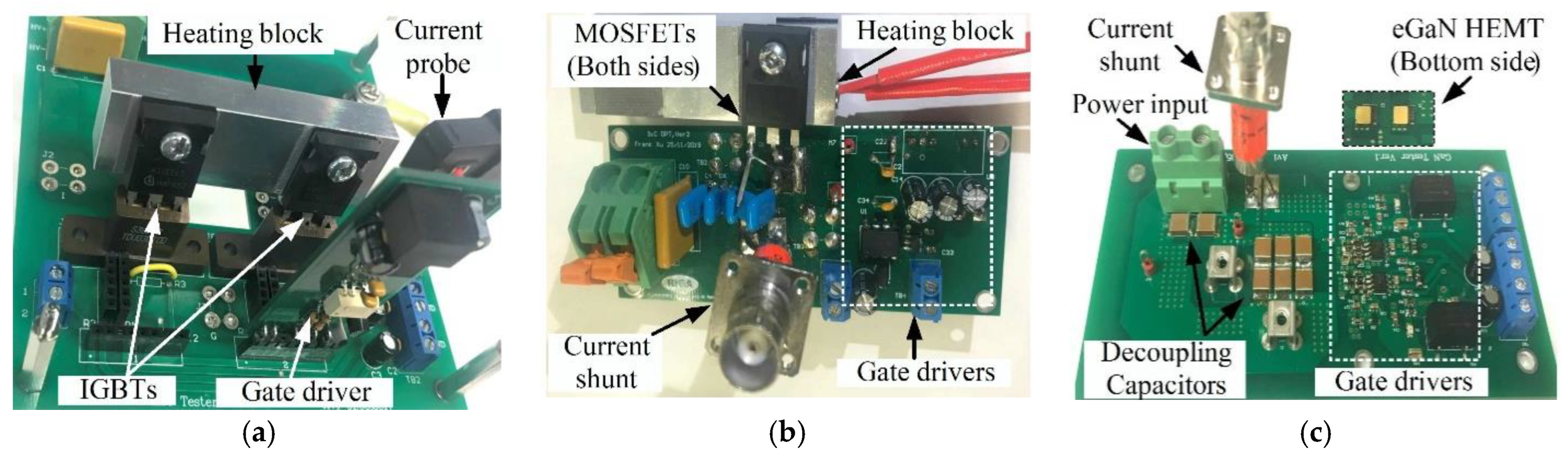
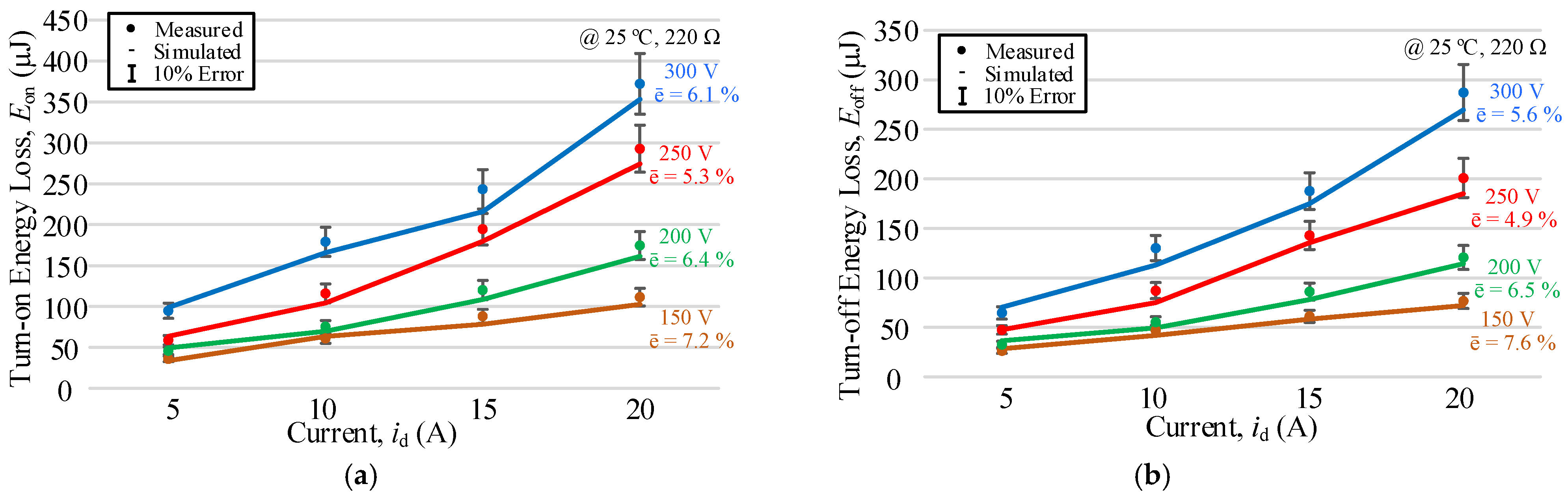
- A DPT setup was designed for experimental verification. To meets the different requirements of different semiconductors, three daughter boards were specifically designed incorporating with the main control board to characterize various devices and measure the corresponding power losses in a wide range of operating conditions. The simulated results are compared with the experimental results and show good agreements within 10% average error range.
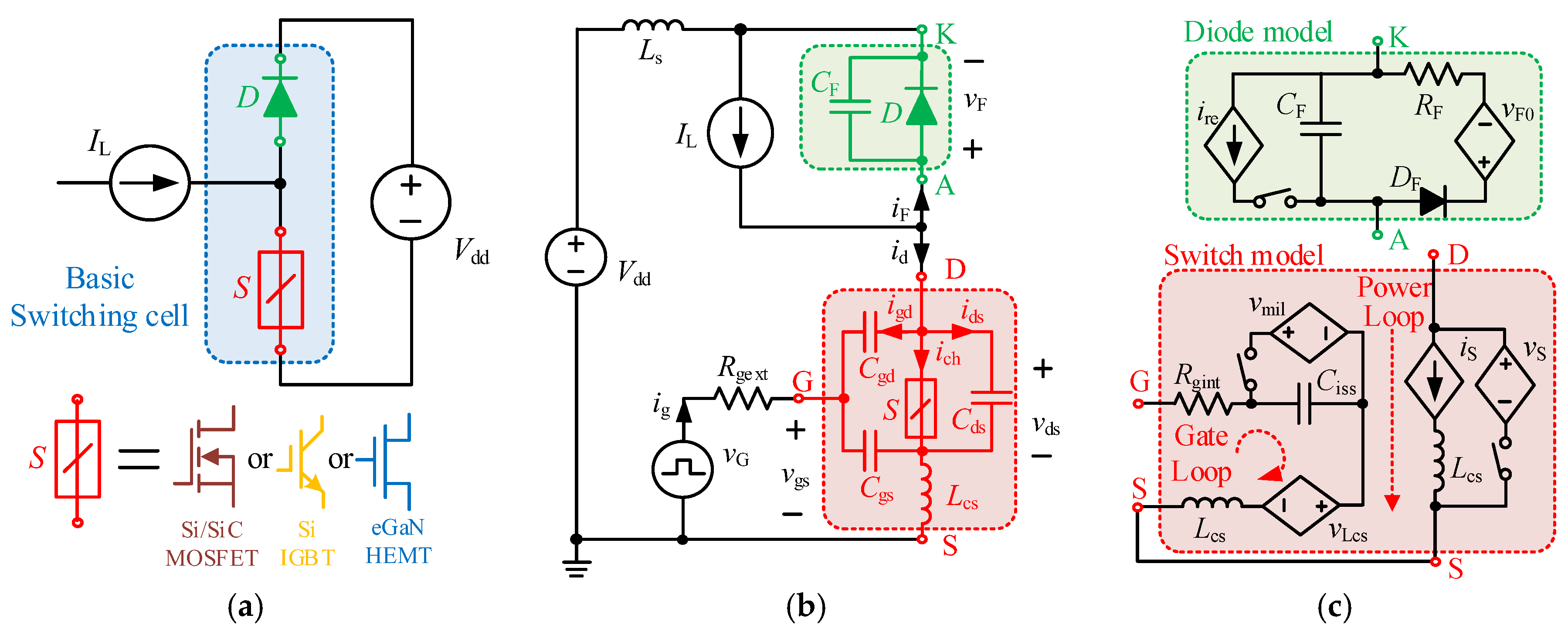
2. Model Description
2.1. Active Switch Model
- Gate Loop Part
- Power Loop Part
2.2. Diode Model
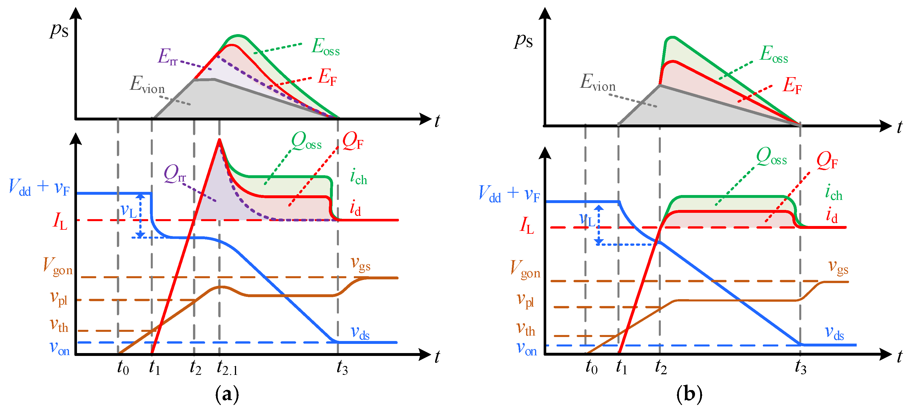
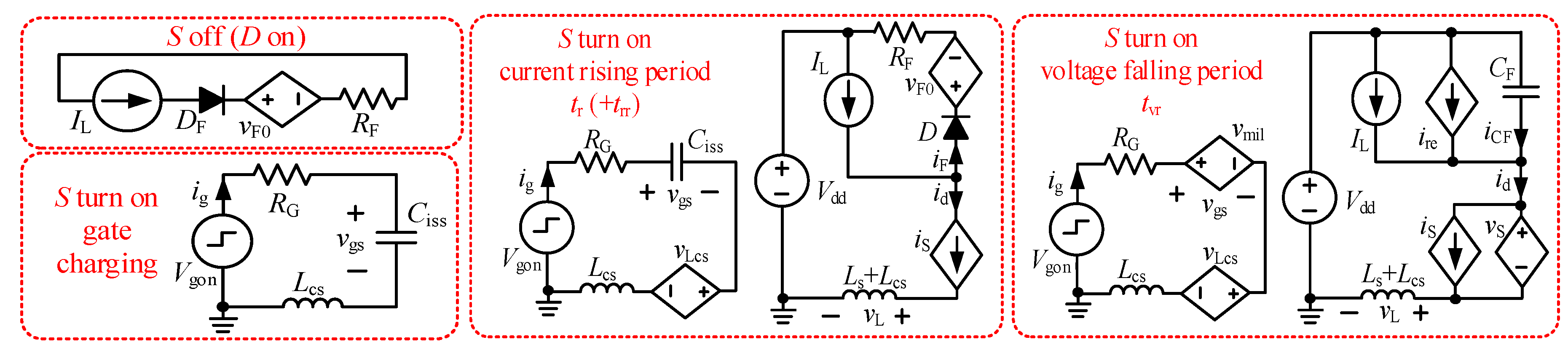
2.3. Switching Transient Modelling
- Turn-on transition ( − )
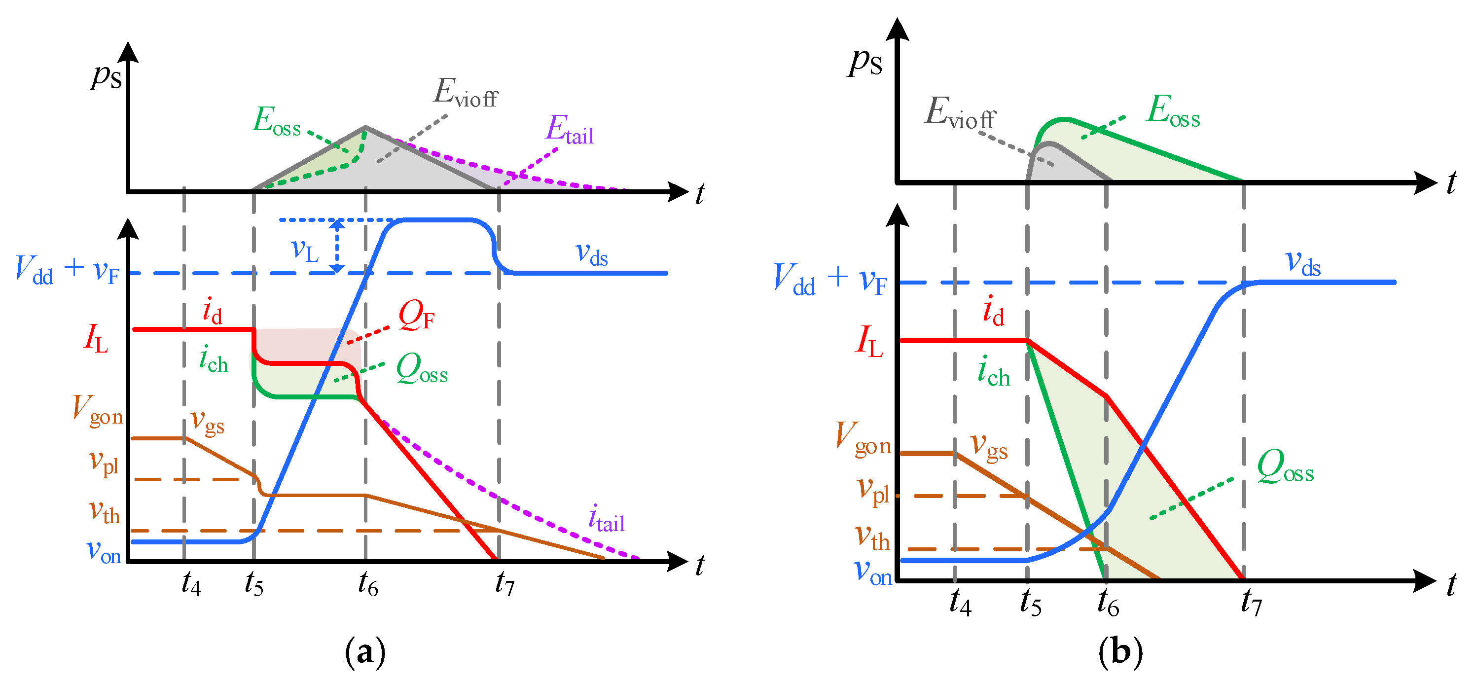
- Turn-off transition ( − )
3. Power Loss Analysis and Parameter Extraction
3.1. Turn on Loss()
3.2. Turn off Loss()
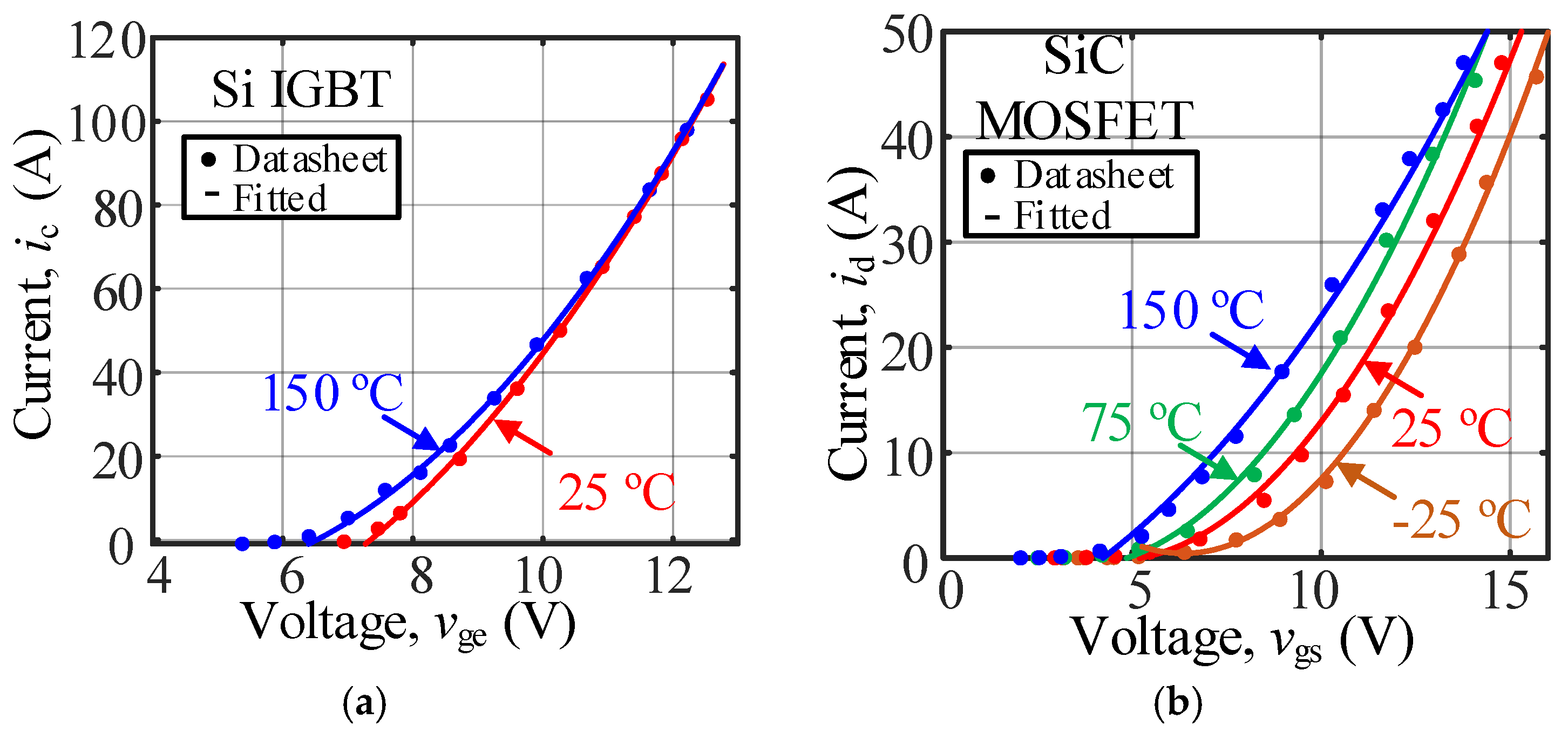
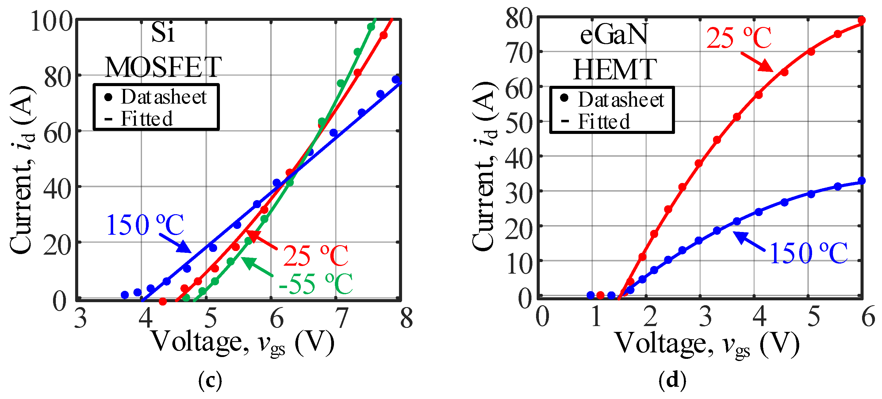
3.3. Parameter Extraction
- Static characteristic
- Parasitic capacitance and inductance
- Diode parameters
4. Experimental Verification
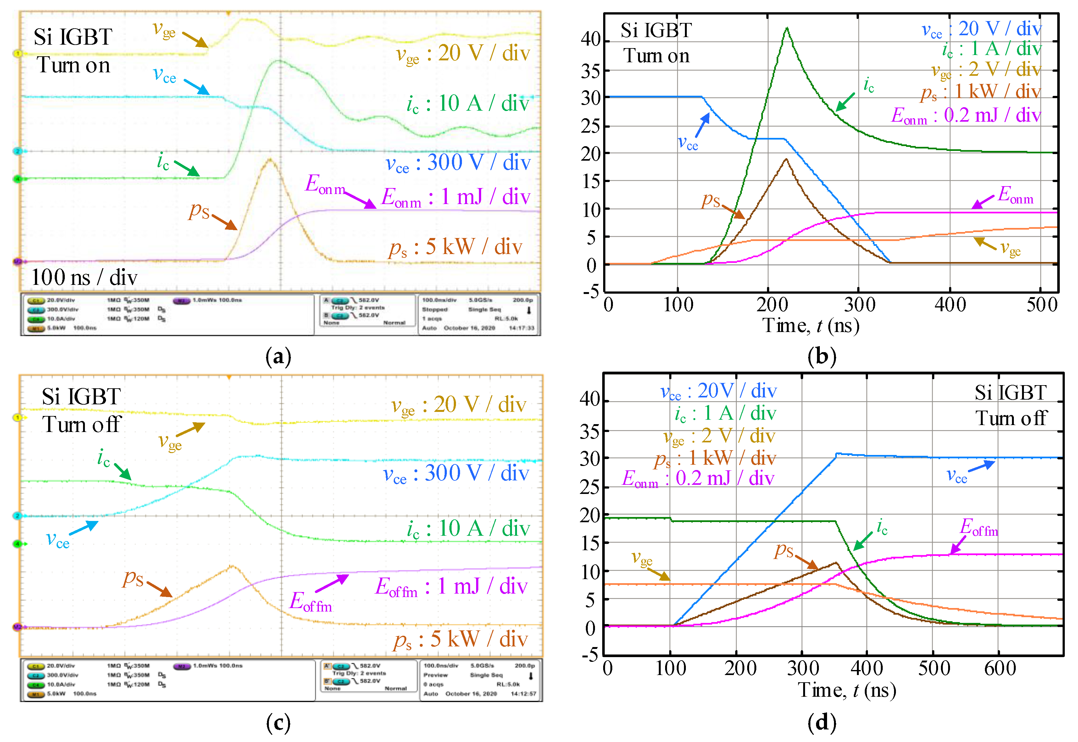
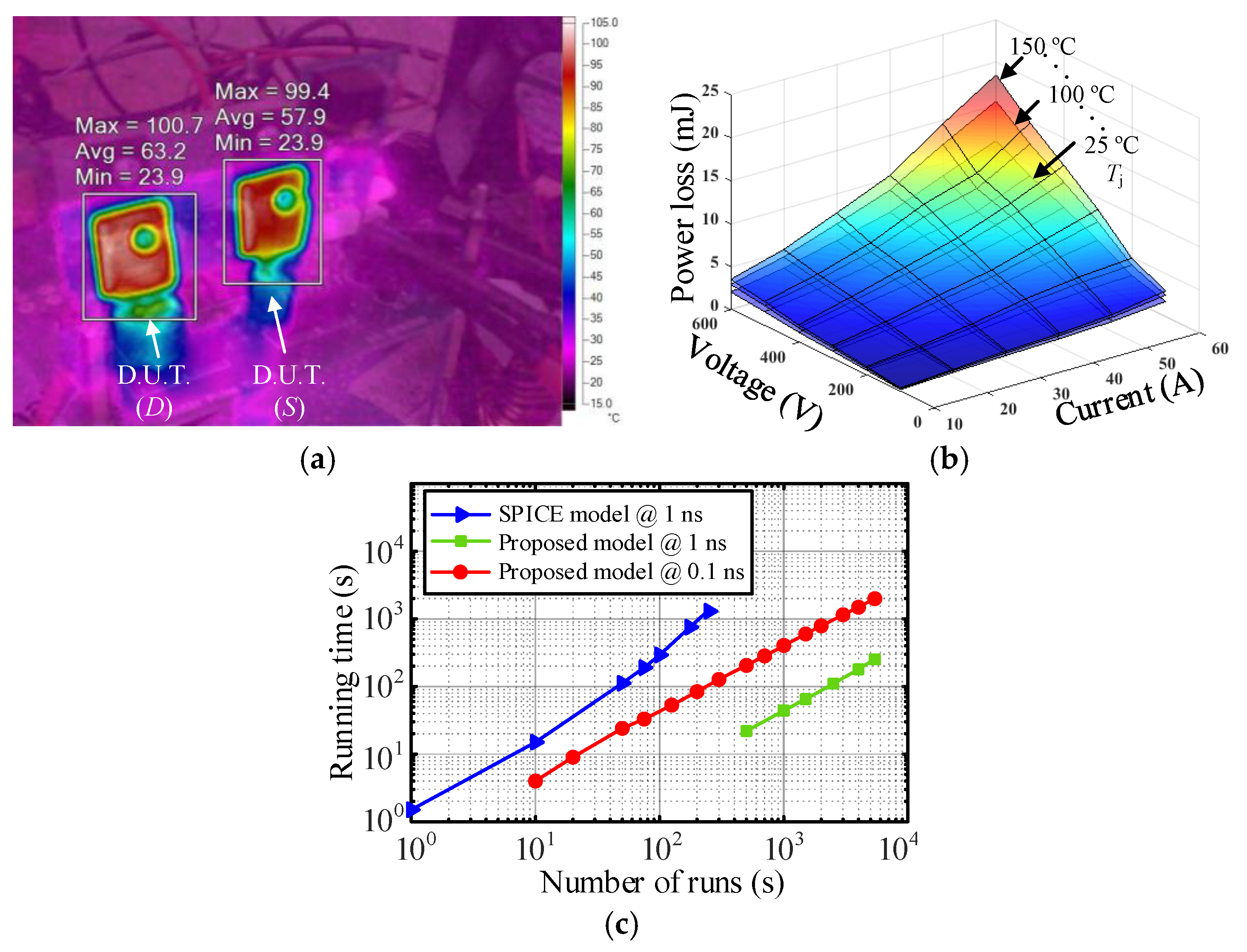
4.1. Setup Description
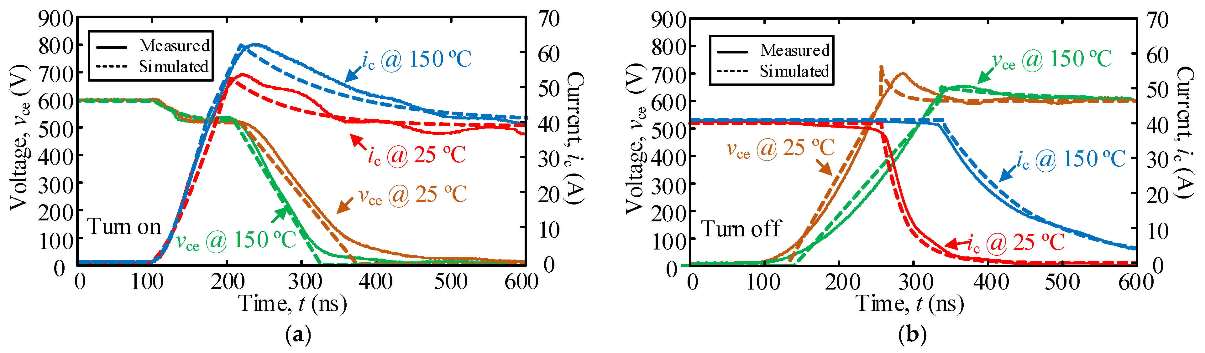
4.2. Switching Transient Verification
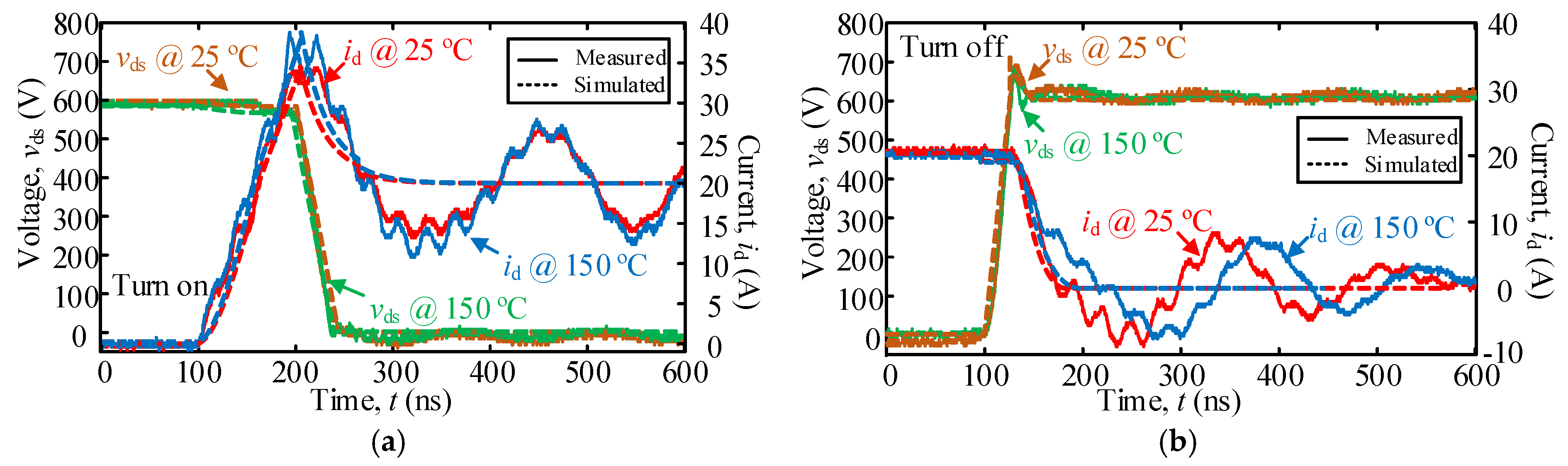
- Si IGBT
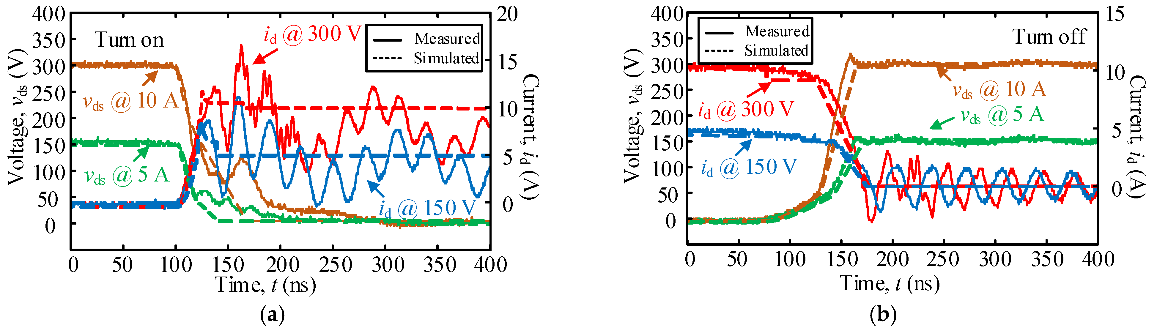
- SiC MOSFET
- Si MOSFET with SiC diode
- eGaN HEMT
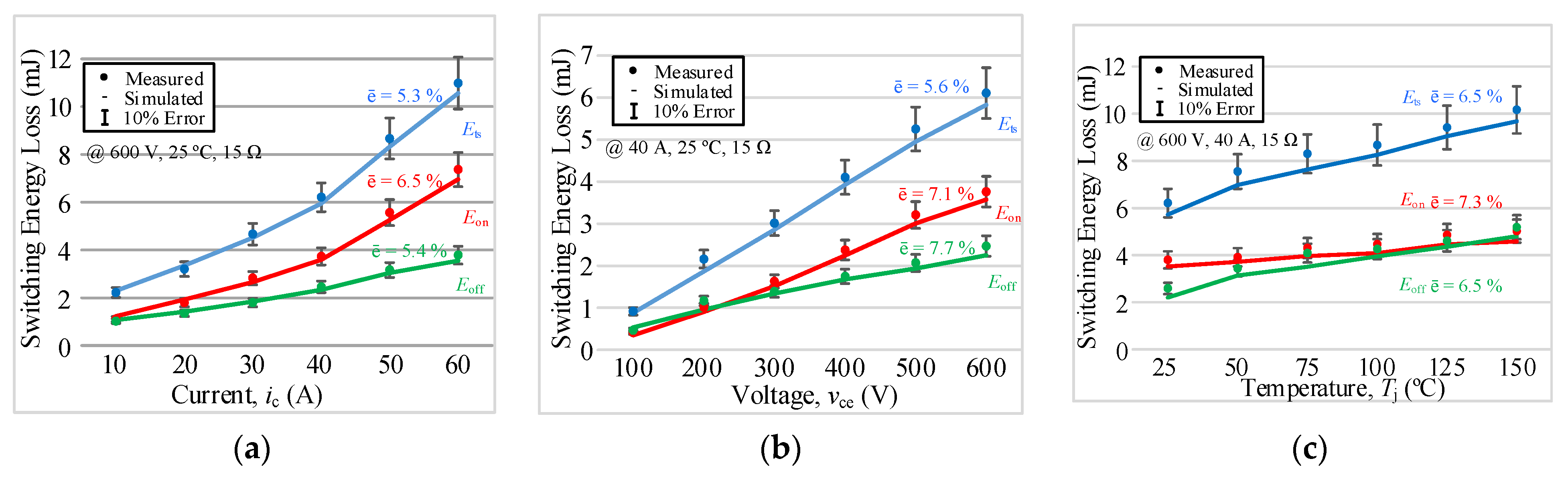
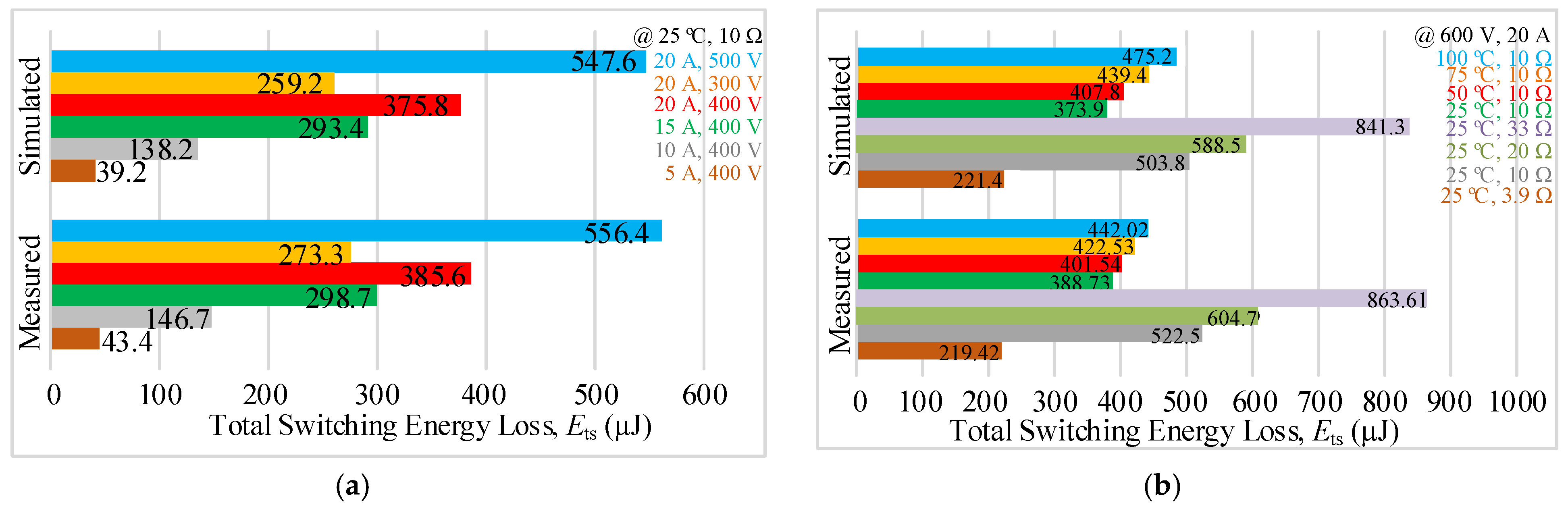
4.3. Power Loss Verification
4.4. Discussion
- Accuracy
- Efficiency
- Applicability
5. Conclusions
Author Contributions
Funding
Institutional Review Board Statement
Informed Consent Statement
Data Availability Statement
Conflicts of Interest
References
- Baliga, B.J. Fundamentals of Power Semiconductor Devices; Springer: New York, NY, USA, 2008. [Google Scholar]
- Iwamuro, N.; Laska, T. IGBT History, State-of-the-Art, and Future Prospects. IEEE Trans. Electron. Devices 2017, 64, 741–752. [Google Scholar] [CrossRef]
- Grant, D.A.; Gowar, J. Power MOSFET Theory and Applications; Wiley: New York, NY, USA, 1989. [Google Scholar]
- Islam, M.; Mekhilef, S. Efficient Transformerless MOSFET Inverter for a Grid-Tied Photovoltaic System. IEEE Trans. Power Electron. 2016, 31, 6305–6316. [Google Scholar] [CrossRef]
- Zhang, Y.; Yao, C.; Zhang, X.; Chen, H.; Li, H.; Wang, J. Power Loss Model for GaN-Based MHz Critical Conduction Mode Power Factor Correction Circuits. IEEE Trans. Emerg. Sel. Top. Power Electron. 2020, 8, 141–151. [Google Scholar] [CrossRef]
- Yang, B.; Wang, J.; Xu, S.; Korec, J.; Shen, Z.J. Advanced Low-Voltage Power MOSFET Technology for Power Supply in Package Applications. IEEE Trans. Power Electron. 2013, 28, 4202–4215. [Google Scholar] [CrossRef]
- Marroqui, D.; Garrigós, A.; Torres, C.; Orts, C.; Blanes, J.M.; Gutierrez, R. Interleaved, Switched Inductor and High-Gain Wide Bandgap Based Boost Converter Proposal. Energies 2021, 14, 800. [Google Scholar] [CrossRef]
- Waradzyn, Z.; Stala, R.; Mondzik, A.; Skała, A.; Penczek, A. GaN-Based DC-DC Resonant Boost Converter with Very High Eciency and Voltage Gain Control. Energies 2020, 13, 6403. [Google Scholar] [CrossRef]
- Millán, J.; Godignon, P.; Perpiñà, X.; Pérez-Tomás, A.; Rebollo, J. A Survey of Wide Bandgap Power Semiconductor Devices. IEEE Trans. Power Electron. 2014, 29, 2155–2163. [Google Scholar] [CrossRef]
- Cha, K.H.; Ju, C.T.; Kim, R.Y. Analysis and Evaluation of WBG Power Device in High Frequency Induction Heating Application. Energies 2020, 13, 5351. [Google Scholar] [CrossRef]
- Li, X.B.; Ma, H.B.; Yi, J.H.; Lu, S.; Xu, J.P. A Comparative Study of GaN HEMT and Si MOSFET-Based Active Clamp Forward Converters. Energies 2020, 13, 4160. [Google Scholar] [CrossRef]
- Cooper, J.A.; Melloch, M.R.; Singh, R.; Agarwal, A.; Palmour, J.W. Status and prospects for SiC power MOSFETs. IEEE Trans. Electron. Devices 2002, 49, 658–664. [Google Scholar] [CrossRef]
- Lidow, A.; Rooij, M.d.; Strydom, J.; Reusch, D.; Glaser, J. GaN Transistors for Efficient Power Conversion, 3rd ed.; Wiley: Hoboken, NJ, USA, 2020; pp. 1–23. [Google Scholar]
- Jones, E.A.; Wang, F.F.; Costinett, D. Review of Commercial GaN Power Devices and GaN-Based Converter Design Challenges. IEEE Trans. Emerg. Sel. Top. Power Electron. 2016, 4, 707–719. [Google Scholar] [CrossRef]
- Bryant, A.T.; Mawby, P.A.; Palmer, P.R.; Santi, E.; Hudgins, J.L. Exploration of power device reliability using compact device models and fast electrothermal simulation. IEEE Trans. Ind. Appl. 2008, 44, 894–903. [Google Scholar] [CrossRef]
- Gole, A.M.; Keri, A.; Kwankpa, C.; Gunther, E.W.; Dommel, H.W.; Hassan, I.; Marti, J.R.; Martinez, J.A.; Fehrle, K.G.; Tang, L.; et al. Guidelines for modelling power electronics in electric power engineering applications. IEEE Trans. Power Del. 1997, 12, 505–514. [Google Scholar] [CrossRef]
- Ghosh, A.; Ho, C.; Prendergast, J.; Xu, Y. Conceptual Design and Demonstration of an Automatic System for Extracting Switching Loss and Creating Data Library of Power Semiconductors. IEEE Open J. Power Electron. 2020, 1, 431–444. [Google Scholar] [CrossRef]
- Mantooth, H.A.; Peng, K.; Santi, E.; Hudgins, J.L. Modelling of Wide Bandgap Power Semiconductor Devices—Part, I. IEEE Trans. Electron. Devices 2015, 62, 423–433. [Google Scholar] [CrossRef]
- Kraus, R.; Castellazzi, A. A Physics-Based Compact Model of SiC Power MOSFETs. IEEE Trans. Power Electron. 2016, 31, 5863–5870. [Google Scholar] [CrossRef]
- McNutt, T.R.; Hefner, A.R.; Mantooth, H.A.; Berning, D.; Ryu, S. Silicon Carbide Power MOSFET Model and Parameter Extraction Sequence. IEEE Trans. Power Electron. 2007, 22, 353–363. [Google Scholar] [CrossRef]
- Mudholkar, M.; Ahmed, S.; Ericson, M.N.; Frank, S.S.; Britton, C.L.; Mantooth, H.A. Datasheet Driven Silicon Carbide Power MOSFET Model. IEEE Trans. Power Electron. 2014, 29, 2220–2228. [Google Scholar] [CrossRef]
- Li, H.; Zhao, X.; Su, W.; Sun, K.; You, X.; Zheng, T.Q. Nonsegmented PSpice Circuit Model of GaN HEMT with Simulation Convergence Consideration. IEEE Trans. Ind. Electron. 2017, 64, 8992–9000. [Google Scholar] [CrossRef]
- Li, H.; Zhao, X.; Sun, K.; Zhao, Z.; Cao, G.; Zheng, T.Q. A Non-Segmented PSpice Model of SiC mosfet With Temperature-Dependent Parameters. IEEE Trans. Power Electron. 2019, 34, 4603–4612. [Google Scholar] [CrossRef]
- Turzynski, M.; Kulesza, W.J. A Simplified Behavioral MOSFET Model Based on Parameters Extraction for Circuit Simulations. IEEE Trans. Power Electron. 2016, 31, 3096–3105. [Google Scholar] [CrossRef]
- Wen, Y.; Yang, Y.; Gao, Y. Model parameter calibration method of SiC power MOSFETs behavioural model. IET Power Electron. 2020, 13, 426–435. [Google Scholar] [CrossRef]
- Ren, Y.; Xu, M.; Zhou, J.; Lee, F.C. Analytical loss model of power MOSFET. IEEE Trans. Power Electron. 2006, 21, 310–319. [Google Scholar]
- Rąbkowski, J.; Skoneczny, H.; Kopacz, R.; Trochimiuk, P.; Wrona, G. A Simple Method to Validate Power Loss in Medium Voltage SiC MOSFETs and Schottky Diodes Operating in a Three-Phase Inverter. Energies 2020, 13, 4773. [Google Scholar] [CrossRef]
- Mukunoki, Y.; Konno, K.; Tsubasa, M.; Horiguchi, T.; Nishizawa, A.; Kuzumoto, M.; Hagiwara, M.; Akagi, H. An Improved Compact Model for a Silicon-Carbide MOSFET, and its Application to Accurate Circuit Simulation. IEEE Trans. Power Electron. 2018, 33, 9834–9842. [Google Scholar] [CrossRef]
- Jin, M.; Gao, Q.; Wang, Y.; Xu, D. A Temperature-Dependent SiC MOSFET Modelling Method Based on MATLAB/Simulink. IEEE Access 2017, 6, 4497–4505. [Google Scholar] [CrossRef]
- Riccio, M.; D’Alessandro, V.; Romano, G.; Maresca, L.; Breglio, G.; Irace, A. A Temperature-Dependent SPICE Model of SiC Power MOSFETs for Within and Out-of-SOA Simulations. IEEE Trans. Power Electron. 2018, 33, 8020–8029. [Google Scholar] [CrossRef]
- Shi, B.; Zhao, Z.; Zhu, Y. Piecewise Analytical Transient Model for Power Switching Device Commutation Unit. IEEE Trans. Power Electron. 2019, 34, 5720–5736. [Google Scholar] [CrossRef]
- Yuan, D.; Zhang, Y.; Wang, X. An Improved Analytical Model for Crosstalk of SiC MOSFET in a Bridge-Arm Configuration. Energies 2021, 14, 683. [Google Scholar] [CrossRef]
- Wang, X.; Zhao, Z.; Li, K.; Zhu, Y.; Chen, K. Analytical Methodology for Loss Calculation of SiC MOSFETs. IEEE Trans. Emerg. Sel. Top. Power Electron. 2019, 7, 71–83. [Google Scholar] [CrossRef]
- Xie, R.; Wang, H.; Tang, G.; Yang, X.; Chen, K.J. An Analytical Model for False Turn-On Evaluation of High-Voltage Enhancement-Mode GaN Transistor in Bridge-Leg Configuration. IEEE Trans. Power Electron. 2017, 32, 6416–6433. [Google Scholar] [CrossRef]
- Agrawal, B.; Freindl, M.; Bilgin, B.; Emadi, A. Estimating switching losses for SiC MOSFETs with non-flat miller plateau region. In Proceedings of the 2017 IEEE Applied Power Electronics Conference and Exposition (APEC), Tampa, FL, USA, 26–30 March 2017; pp. 2664–2670. [Google Scholar]
- Wang, K.; Yang, X.; Li, H.; Ma, H.; Zeng, X.; Chen, W. An Analytical Switching Process Model of Low-Voltage eGaN HEMTs for Loss Calculation. IEEE Trans. Power Electron. 2016, 31, 635–647. [Google Scholar] [CrossRef]
- Chen, J.; Luo, Q.; Huang, J.; He, Q.; Du, X. A Complete Switching Analytical Model of Low-Voltage eGaN HEMTs and Its Application in Loss Analysis. IEEE Trans. Ind. Electron. 2020, 67, 1615–1625. [Google Scholar] [CrossRef]
- Gareau, J.; Hou, R.; Emadi, A. Review of Loss Distribution, Analysis, and Measurement Techniques for GaN HEMTs. IEEE Trans. Power Electron. 2020, 35, 7405–7418. [Google Scholar] [CrossRef]
- Hou, R.; Lu, J.; Chen, D. Parasitic capacitance Eqoss loss mechanism, calculation, and measurement in hard-switching for GaN HEMTs. In Proceedings of the 2018 IEEE Applied Power Electronics Conference and Exposition (APEC), San Antonio, TX, USA, 4–8 March 2018; pp. 919–924. [Google Scholar]
- Ho, C.; Breuninger, S.; Pettersson, G.; Escobar, L. Serpa, and A. Coccia. Practical design and implementation procedure of an interleaved boost converter using SiC diodes for PV applications. IEEE Trans. Power Electron. 2012, 27, 2834–2845. [Google Scholar] [CrossRef]
- Ho, C.; Breuninger, H.; Pettersson, S.; Escobar, G.; Canales, F. A comparative performance study of an interleaved boost converter using commercial Si and SiC diodes for PV applications. IEEE Trans. Power Electron. 2013, 28, 289–299. [Google Scholar] [CrossRef]
- Xu, Y.; Ho, C.N.M.; Ghosh, A.; Muthumuni, D. An Electrical Transient Model of IGBT-Diode Switching Cell for Power Semiconductor Loss Estimation in Electromagnetic Transient Simulation. IEEE Trans. Power Electron. 2020, 35, 2979–2989. [Google Scholar] [CrossRef]
- Xu, Y.; Ho, C.N.M.; Ghosh, A.; Muthumuni, D. Design, Implementation and Validation of Electro-Thermal Simulation for SiC MOSFETs in Power Electronic Systems. IEEE Trans. Ind. Appl. 2021. [Google Scholar] [CrossRef]
- Reiner, R.; Waltereit, P.; Weiss, B.; Quay, R.; Ambacher, O. Investigation of GaN-HEMTs in Reverse Conduction. In Proceedings of the PCIM Asia, International Exhibition and Conference for Power Electronics, Intelligent Motion, Renewable Energy and Energy Management, Nuremberg, Germany, 16–18 March 2017; pp. 1–8. [Google Scholar]
- Lauritzen, P.O.; Ma, C.L. A Simple Diode Model with Reverse Recovery. IEEE Trans. Power Electron. 1991, 6, 188–191. [Google Scholar] [CrossRef]
- Jarndal, A.; Essaadali, R.; Kouki, A.B. A Reliable Model Parameter Extraction Method Applied to AlGaN/GaN HEMTs. IEEE Trans. Comput. Aided Design Integr. Circuits Syst. 2016, 35, 211–219. [Google Scholar] [CrossRef]
- Jouha, W.; El Oualkadi, A.; Dherbécourt, P.; Joubert, E. Silicon Carbide Power MOSFET Model: An Accurate Parameter Extraction Method Based on Levenberg-Marquardt Algorithm. IEEE Trans. Power Electron. 2018, 33, 9130–9133. [Google Scholar] [CrossRef]
- Bryant, A.T.; Kang, X.; Santi, E.; Palmer, P.R.; Hudgins, J.L. Two-step parameter extraction procedure with formal optimization for physics-based circuit simulator IGBT and p-i-n diode models. IEEE Trans. Power Electron. 2006, 21, 295–309. [Google Scholar] [CrossRef]
- Ahmed, M.R.; Todd, R.; Forsyth, A.J. Predicting SiC MOSFET Behavior Under Hard-Switching, Soft-Switching, and False Turn-On Conditions. IEEE Trans. Ind. Electron. 2017, 64, 9001–9011. [Google Scholar] [CrossRef]
- Howard, J.; Martin, G. High-Speed Digital Design: A Handbook of Black Magic; Pearson Education: London, UK, 1999. [Google Scholar]
- Stueckler, F.; Vecino, E. CoolMOS C7 650V Switch in a Kelvin Source Configuration; Infineon Technology. Application Note AN 2013-05; Infineon Technologies: Neubiberg, Germany, 2013. [Google Scholar]


| Condition | Tail Period for IGBT | Turn-off for eGaN HEMT | ||||
| Expression | 0 | (7) | (10) | (12) | (14) |
| Device Type | Si IGBT | SiC MOSFET | Si MOSFET | eGaN HEMT | SiC SBD |
|---|---|---|---|---|---|
| Part Number | IKW40T120 | SCT2080KE | NVHL072N65S3 | GS66506T | SCS220KG |
| Manufacturer | Infineon | Rohm | On Semiconductor | GaN System | ROHM |
| Parameter | ||||||||
|---|---|---|---|---|---|---|---|---|
| Si IGBT | 2.05 | −6.96 | 14.2 | −0.012 | −0.001 | 0.972 | 0.0215 | |
| SiC MOSFET | 0.42 | −0.35 | 2.96 | −0.086 | 0.073 | |||
| Si MOSFET | 3.72 | −19.2 | 13 | −0.57 | 0.048 | 0.034 | 0.0012 | |
| eGaN HEMT | 0.23 | −776.9 | 0.51 | −0.31 | 0.067 |
| DUT Case | Si IGBT | SiC MOSFET | Si MOSFET | eGaN HEMT |
|---|---|---|---|---|
| Probes calibration (ns) | 48 | 26 | 45 | 23 |
| Turn-on calibration (ns) | 35 | 13 | 26 | 14 |
| Turn-off calibration (ns) | 31 | 18 | 25 | 12 |
Publisher’s Note: MDPI stays neutral with regard to jurisdictional claims in published maps and institutional affiliations. |
© 2021 by the authors. Licensee MDPI, Basel, Switzerland. This article is an open access article distributed under the terms and conditions of the Creative Commons Attribution (CC BY) license (http://creativecommons.org/licenses/by/4.0/).
Share and Cite
Xu, Y.; Ho, C.N.M.; Ghosh, A.; Muthumuni, D. Generalized Behavioral Modelling Methodology of Switch-Diode Cell for Power Loss Prediction in Electromagnetic Transient Simulation. Energies 2021, 14, 1500. https://doi.org/10.3390/en14051500
Xu Y, Ho CNM, Ghosh A, Muthumuni D. Generalized Behavioral Modelling Methodology of Switch-Diode Cell for Power Loss Prediction in Electromagnetic Transient Simulation. Energies. 2021; 14(5):1500. https://doi.org/10.3390/en14051500
Chicago/Turabian StyleXu, Yanming, Carl Ngai Man Ho, Avishek Ghosh, and Dharshana Muthumuni. 2021. "Generalized Behavioral Modelling Methodology of Switch-Diode Cell for Power Loss Prediction in Electromagnetic Transient Simulation" Energies 14, no. 5: 1500. https://doi.org/10.3390/en14051500
APA StyleXu, Y., Ho, C. N. M., Ghosh, A., & Muthumuni, D. (2021). Generalized Behavioral Modelling Methodology of Switch-Diode Cell for Power Loss Prediction in Electromagnetic Transient Simulation. Energies, 14(5), 1500. https://doi.org/10.3390/en14051500