
Design Space Optimization of a Three-Phase LCL Filter for Electric Vehicle Ultra-Fast Battery Charging †


Abstract
1. Introduction
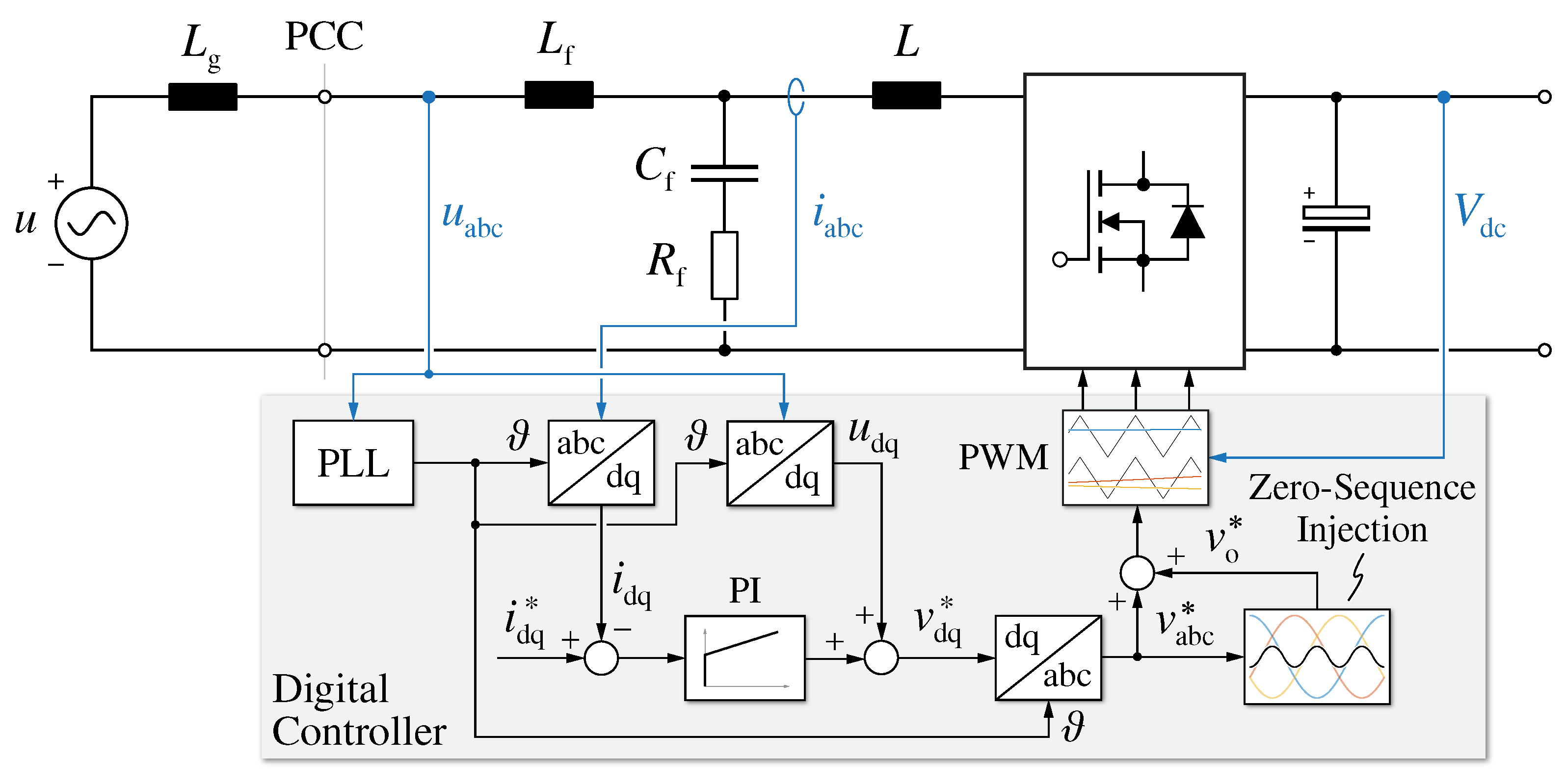
2. Filter Model
3. Design Procedure
3.1. Specifications and Performance Targets
3.2. Parameters and Constraints
- The filter resonance frequency must be higher than 10 times the grid frequency (), to avoid resonance interactions in the lower part of the harmonic spectrum and allow for a sufficient current control bandwidth (i.e., ).
- The filter resonance frequency must be lower than half of the switching frequency (), to avoid unwanted amplification of switching harmonics. Even if damped, the resonance peak tends to amplify the nearby harmonics (see Figure 4c), which may thus exceed the IEEE 519 limits.
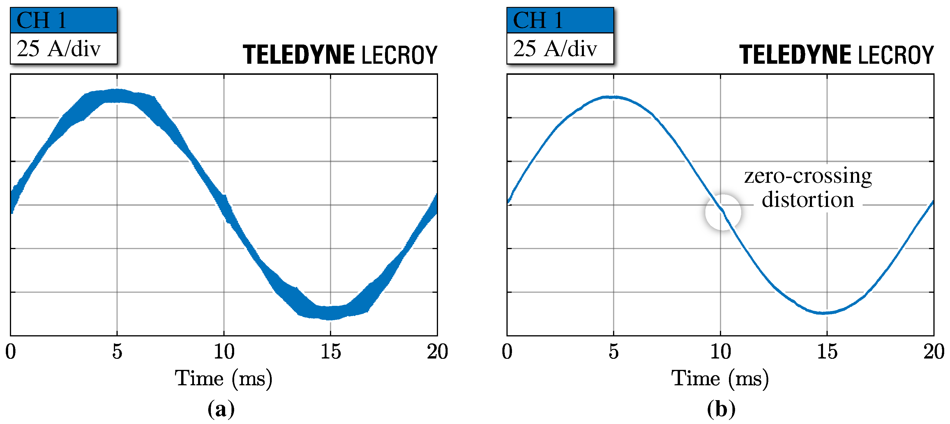
- The current ripple in the converter-side inductor L must be kept below a specified amount to avoid excessive losses in the semiconductor devices (i.e., conduction and switching losses) and in the inductors themselves (i.e., winding and core losses). Moreover, in the present unidirectional case, this current ripple must be limited to narrow the discontinuous conduction mode operation around the waveform zero-crossings, which causes low-frequency harmonic distortion [54]. This limit is set to 20% of the peak nominal current ().
- The maximum voltage drop in nominal load conditions must be lower than a specified value depending on the high-line grid voltage (), the maximum modulation index of the active rectifier (, with ) and the minimum DC-link voltage , resulting in .
- The maximum no-load reactive power generation is set to 10% of the nominal power (). The reactive current circulation generates losses in the system components (i.e., the LCL filter and the distribution equipment), therefore it must be limited accordingly.
- The minimum power factor at a specified minimum load condition () is set to , taking into account that the unidirectional rectifier cannot generate or absorb reactive power without affecting the low-frequency input current distortion. is selected taking into account that the adopted modular structure (see Figure 7) allows to turn-off selected converter modules with decreasing load, thus ensuring high power factor over the complete charging range.
- The minimum filter attenuation must ensure that the injected current harmonics comply with the IEEE 519 limits (see Table 2). An additional margin of 50% (i.e., ), taking into account component tolerances and unmodeled factors, is assumed herein.
3.3. Filter Design Space
4. Simulation and Experimental Results
4.1. Filter Transfer Functions
4.2. Filter Attenuation
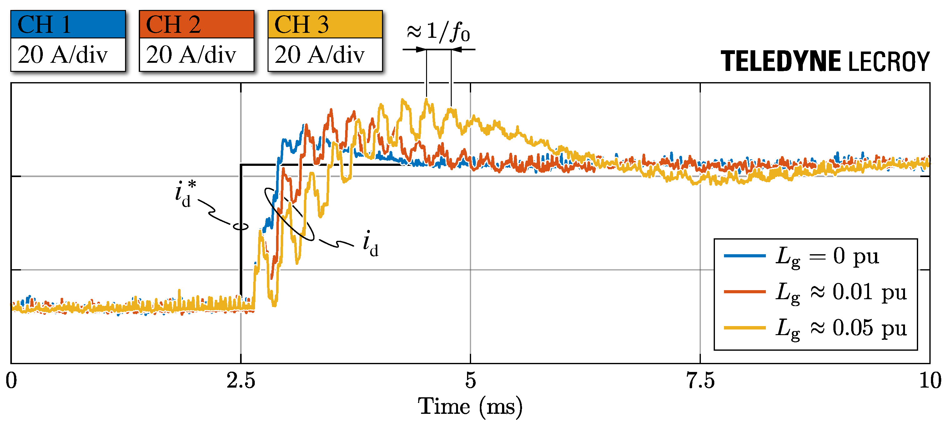
4.3. Converter Control Stability and Dynamic Response
5. Conclusions
Author Contributions
Funding
Conflicts of Interest
References
- Manzetti, S.; Mariasiu, F. Electric Vehicle Battery Technologies: From Present State to Future Systems. Renew. Sustain. Energy Rev. 2015, 51, 1004–1012. [Google Scholar] [CrossRef]
- Clement-Nyns, K.; Haesen, E.; Driesen, J. The Impact of Charging Plug-In Hybrid Electric Vehicles on a Residential Distribution Grid. IEEE Trans. Power Syst. 2010, 25, 371–380. [Google Scholar] [CrossRef]
- Tu, H.; Feng, H.; Srdic, S.; Lukic, S. Extreme Fast Charging of Electric Vehicles: A Technology Overview. IEEE Trans. Transp. Electrif. 2019, 5, 861–878. [Google Scholar] [CrossRef]
- Mandrile, F.; Cittanti, D.; Mallemaci, V.; Bojoi, R. Electric Vehicle Ultra-Fast Battery Chargers: A Boost for Power System Stability? World Electr. Veh. J. 2021, 12, 16. [Google Scholar] [CrossRef]
- Nicholas, M.; Hall, D. Lessons Learned on Early Electric Vehicle Fast-Charging Deployments. Int. Counc. Clean Transp. 2018, 7–26. Available online: https://www.theicct.org/sites/default/files/publications/ZEV_fast_charging_white_paper_final.pdf (accessed on 21 February 2020).
- IEA. Global EV Outlook 2020–Analysis. 2020. Available online: https://www.iea.org/reports/global-ev-outlook-2020 (accessed on 21 February 2020).
- Aggeler, D.; Canales, F.; Zelaya-De La Parra, H.; Coccia, A.; Butcher, N.; Apeldoorn, O. Ultra-Fast DC-Charge Infrastructures for EV-Mobility and Future Smart Grids. In Proceedings of the IEEE Innovative Smart Grid Technologies Conference Europe (ISGT Europe), Gothenburg, Sweden, 11–13 October 2010. [Google Scholar] [CrossRef]
- Yilmaz, M.; Krein, P.T. Review of Battery Charger Topologies, Charging Power Levels, and Infrastructure for Plug-In Electric and Hybrid Vehicles. IEEE Trans. Power Electron. 2013, 28, 2151–2169. [Google Scholar] [CrossRef]
- Channegowda, J.; Pathipati, V.K.; Williamson, S.S. Comprehensive Review and Comparison of DC Fast Charging Converter Topologies: Improving Electric Vehicle Plug-to-Wheels Efficiency. In Proceedings of the IEEE International Symposium on Industrial Electronics (ISIE), Buzios, Brazil, 3–5 June 2015; pp. 263–268. [Google Scholar] [CrossRef]
- Cittanti, D.; Gregorio, M.; Bojoi, R. Digital Multi-Loop Control of a 3-Level Rectifier for Electric Vehicle Ultra-Fast Battery Chargers. In Proceedings of the AEIT International Annual Conference (AEIT), Catania, Italy, 23–25 September 2020. [Google Scholar] [CrossRef]
- Cittanti, D.; Gregorio, M.; Armando, E.; Bojoi, R. Digital Multi-Loop Control of an LLC Resonant Converter for Electric Vehicle DC Fast Charging. In Proceedings of the IEEE Energy Conversion Congress and Exposition (ECCE), Detroit, MI, USA, 11–15 October 2020; pp. 4423–4430. [Google Scholar] [CrossRef]
- De Breucker, S.; Engelen, K.; D’hulst, R.; Driesen, J. Impact of Current Ripple on Li-ion Battery Ageing. World Electr. Veh. J. 2013, 6, 532–540. [Google Scholar] [CrossRef]
- Teichmann, R.; Bernet, S. A Comparison of Three-Level Converters versus Two-Level Converters for Low-Voltage Drives, Traction, and Utility Applications. IEEE Trans. Ind. Appl. 2005, 41, 855–865. [Google Scholar] [CrossRef]
- Schweizer, M.; Friedli, T.; Kolar, J.W. Comparative Evaluation of Advanced Three-Phase Three-Level Inverter/Converter Topologies Against Two-Level Systems. IEEE Trans. Ind. Electron. 2013, 60, 5515–5527. [Google Scholar] [CrossRef]
- Kolar, J.W.; Friedli, T. The Essence of Three-Phase PFC Rectifier Systems—Part I. IEEE Trans. Power Electron. 2013, 28, 176–198. [Google Scholar] [CrossRef]
- Cittanti, D.; Guacci, M.; Mirić, S.; Bojoi, R.; Kolar, J.W. Comparative Evaluation of 800V DC-Link Three-Phase Two/Three-Level SiC Inverter Concepts for Next-Generation Variable Speed Drives. In Proceedings of the International Conference on Electrical Machines and Systems (ICEMS), Hamamatsu, Japan, 24–27 November 2020; pp. 1699–1704. [Google Scholar] [CrossRef]
- Ogasawara, S.; Akagi, H. Analysis of Variation of Neutral Point Potential in Neutral-Point-Clamped Voltage Source PWM Inverters. In Proceedings of the IEEE Industry Applications Conference, Toronto, ON, Canada, 2–8 October 1993; pp. 965–970. [Google Scholar] [CrossRef]
- Kolar, J.W.; Drofenik, U.; Zach, F.C. On the Interdependence of AC-Side and DC-Side Optimum Control of Three-Phase Neutral-Point-Clamped (Three-Level) PWM Rectifier Systems. In Proceedings of the International Power Electronics and Motion Control Conference (PEMC), Budapest, Hungary, 2–4 September 1996. [Google Scholar]
- Kolar, J.; Drofenik, U.; Zach, F. Current Handling Capability of the Neutral Point of a Three-Phase/Switch/Level Boost-Type PWM (VIENNA) Rectifier. In Proceedings of the IEEE Power Electronics Specialists Conference (PESC), Baveno, Italy, 23–27 June 1996; Volume 2, pp. 1329–1336. [Google Scholar] [CrossRef]
- Cittanti, D.; Bojoi, R. Modulation Strategy Assessment for 3-Level Unidirectional Rectifiers in Electric Vehicle Ultra-Fast Charging Applications. In Proceedings of the AEIT International Conference of Electrical and Electronic Technologies for Automotive (AEIT AUTOMOTIVE), Turin, Italy, 18–20 November 2020. [Google Scholar] [CrossRef]
- IEEE Recommended Practice and Requirements for Harmonic Control in Electric Power Systems. In IEEE Std 519-2014; IEEE: New York, NY, USA, 2014; pp. 1–29. [CrossRef]
- Jalili, K.; Bernet, S. Design of LCL Filters of Active-Front-End Two-Level Voltage-Source Converters. IEEE Trans. Ind. Electron. 2009, 56, 1674–1689. [Google Scholar] [CrossRef]
- Blasko, V.; Kaura, V. A Novel Control to Actively Damp Resonance in Input LC Filter of a Three-Phase Voltage Source Converter. IEEE Trans. Ind. Appl. 1997, 33, 542–550. [Google Scholar] [CrossRef]
- Liserre, M.; Dell’Aquila, A.; Blaabjerg, F. Stability Improvements of an LCL-Filter Based Three-Phase Active Rectifier. In Proceedings of the IEEE Power Electronics Specialists Conference (PESC), Cairns, QLD, Australia, 23–27 June 2002; Volume 3, pp. 1195–1201. [Google Scholar] [CrossRef]
- Dannehl, J.; Liserre, M.; Fuchs, F.W. Filter-Based Active Damping of Voltage Source Converters With LCL Filter. IEEE Trans. Ind. Electron. 2011, 58, 3623–3633. [Google Scholar] [CrossRef]
- Peña-Alzola, R.; Liserre, M.; Blaabjerg, F.; Sebastián, R.; Dannehl, J.; Fuchs, F.W. Analysis of the Passive Damping Losses in LCL-Filter-Based Grid Converters. IEEE Trans. Power Electron. 2013, 28, 2642–2646. [Google Scholar] [CrossRef]
- Han, Y.; Yang, M.; Li, H.; Yang, P.; Xu, L.; Coelho, E.A.A.; Guerrero, J.M. Modeling and Stability Analysis of LCL -Type Grid-Connected Inverters: A Comprehensive Overview. IEEE Access 2019, 7, 114975–115001. [Google Scholar] [CrossRef]
- Raggl, K.; Nussbaumer, T.; Kolar, J.W. Guideline for a Simplified Differential-Mode EMI Filter Design. IEEE Trans. Ind. Electron. 2010, 57, 1031–1040. [Google Scholar] [CrossRef]
- Burkart, R.M.; Kolar, J.W. Overview and Comparison of Grid Harmonics and Conducted EMI Standards for LV Converters Connected to the MV Distribution System. In Proceedings of the Power Electronics South America Conference and Exhibition (PCIM South America), SaõPaulo, Brazil, 11–13 September 2012. [Google Scholar]
- Liserre, M.; Blaabjerg, F.; Hansen, S. Design and Control of an LCL-Filter-Based Three-Phase Active Rectifier. IEEE Trans. Ind. Appl. 2005, 41, 1281–1291. [Google Scholar] [CrossRef]
- Channegowda, P.; John, V. Filter Optimization for Grid Interactive Voltage Source Inverters. IEEE Trans. Ind. Electron. 2010, 57, 4106–4114. [Google Scholar] [CrossRef]
- Reznik, A.; Simões, M.G.; Al-Durra, A.; Muyeen, S.M. LCL Filter Design and Performance Analysis for Grid-Interconnected Systems. IEEE Trans. Ind. Appl. 2014, 50, 1225–1232. [Google Scholar] [CrossRef]
- Peña-Alzola, R.; Liserre, M.; Blaabjerg, F.; Ordonez, M.; Yang, Y. LCL-Filter Design for Robust Active Damping in Grid-Connected Converters. IEEE Trans. Ind. Inform. 2014, 10, 2192–2203. [Google Scholar] [CrossRef]
- Jayalath, S.; Hanif, M. Generalized LCL-Filter Design Algorithm for Grid-Connected Voltage-Source Inverter. IEEE Trans. Ind. Electron. 2017, 64, 1905–1915. [Google Scholar] [CrossRef]
- Jayalath, S.; Hanif, M. An LCL-Filter Design With Optimum Total Inductance and Capacitance. IEEE Trans. Power Electron. 2018, 33, 6687–6698. [Google Scholar] [CrossRef]
- Muhlethaler, J.; Schweizer, M.; Blattmann, R.; Kolar, J.W.; Ecklebe, A. Optimal Design of LCL Harmonic Filters for Three-Phase PFC Rectifiers. IEEE Trans. Power Electron. 2013, 28, 3114–3125. [Google Scholar] [CrossRef]
- Park, K.B.; Kieferndorf, F.D.; Drofenik, U.; Pettersson, S.; Canales, F. Weight Minimization of LCL Filters for High-Power Converters: Impact of PWM Method on Power Loss and Power Density. IEEE Trans. Ind. Appl. 2017, 53, 2282–2296. [Google Scholar] [CrossRef]
- Kolar, J.W.; Drofenik, U.; Biela, J.; Heldwein, M.L.; Ertl, H.; Friedli, T.; Round, S.D. PWM Converter Power Density Barriers. In Proceedings of the Power Conversion Conference (PCC), Nagoya, Japan, 2–5 April 2007. [Google Scholar] [CrossRef]
- Boillat, D.O.; Friedli, T.; Mühlethaler, J.; Kolar, J.W.; Hribernik, W. Analysis of the Design Space of Single-Stage and Two-Stage LC Output Filters of Switched-Mode AC Power Sources. In Proceedings of the IEEE Power and Energy Conference (PEC), Champaign, IL, USA, 24–25 February 2012. [Google Scholar] [CrossRef]
- Cittanti, D.; Mandrile, F.; Bojoi, R. Optimal Design of Grid-Side LCL Filters for Electric Vehicle Ultra-Fast Battery Chargers. In Proceedings of the International Universities Power Engineering Conference (UPEC), Turin, Italy, 1–4 September 2020. [Google Scholar] [CrossRef]
- Burkart, R.; Kolar, J.W. Component Cost Models for Multi-Objective Optimizations of Switched-Mode Power Converters. In Proceedings of the IEEE Energy Conversion Congress (ECCE), Denver, CO, USA, 15–19 September 2013; pp. 2139–2146. [Google Scholar] [CrossRef]
- Park, K.; Burkart, R.M. Filter Hardware Optimization of Grid-Tied Converters: LCL vs. LLCL Filter. In Proceedings of the International Conference on Renewable Energy Research and Applications (ICRERA), Paris, France, 14–17 October 2018; pp. 209–214. [Google Scholar] [CrossRef]
- Dannehl, J.; Fuchs, F.W.; Hansen, S.; Thøgersen, P.B. Investigation of Active Damping Approaches for PI-Based Current Control of Grid-Connected Pulse Width Modulation Converters With LCL Filters. IEEE Trans. Ind. Appl. 2010, 46, 1509–1517. [Google Scholar] [CrossRef]
- Parker, S.G.; McGrath, B.P.; Holmes, D.G. Regions of Active Damping Control for LCL Filters. IEEE Trans. Ind. Appl. 2014, 50, 424–432. [Google Scholar] [CrossRef]
- Peña-Alzola, R.; Liserre, M.; Blaabjerg, F.; Sebastián, R.; Dannehl, J.; Fuchs, F.W. Systematic Design of the Lead-Lag Network Method for Active Damping in LCL-Filter Based Three Phase Converters. IEEE Trans. Ind. Inform. 2014, 10, 43–52. [Google Scholar] [CrossRef]
- Pan, D.; Ruan, X.; Bao, C.; Li, W.; Wang, X. Capacitor-Current-Feedback Active Damping With Reduced Computation Delay for Improving Robustness of LCL-Type Grid-Connected Inverter. IEEE Trans. Power Electron. 2014, 29, 3414–3427. [Google Scholar] [CrossRef]
- Erickson, R. Optimal Single Resistors Damping of Input Filters. In Proceedings of the IEEE Applied Power Electronics Conference and Exposition (APEC), Dallas, TX, USA, 14–18 March 1999; Volume 2, pp. 1073–1079. [Google Scholar] [CrossRef]
- Wang, T.C.Y.; Ye, Z.; Sinha, G.; Yuan, X. Output filter design for a grid-interconnected three-phase inverter. In Proceedings of the IEEE Annual Conference on Power Electronics Specialist (PESC), Acapulco, Mexico, 15–19 June 2003; Volume 2, pp. 779–784. [Google Scholar] [CrossRef]
- Xing, L.; Sun, J. Optimal Damping of Multistage EMI Filters. IEEE Trans. Power Electron. 2012, 27, 1220–1227. [Google Scholar] [CrossRef]
- Wu, W.; He, Y.; Tang, T.; Blaabjerg, F. A New Design Method for the Passive Damped LCL and LLCL Filter-Based Single-Phase Grid-Tied Inverter. IEEE Trans. Ind. Electron. 2013, 60, 4339–4350. [Google Scholar] [CrossRef]
- Beres, R.N.; Wang, X.; Liserre, M.; Blaabjerg, F.; Bak, C.L. A Review of Passive Power Filters for Three-Phase Grid-Connected Voltage-Source Converters. IEEE J. Emerg. Sel. Top. Power Electron. 2016, 4, 54–69. [Google Scholar] [CrossRef]
- Liserre, M.; Teodorescu, R.; Blaabjerg, F. Stability of Photovoltaic and Wind Turbine Grid-Connected Inverters for a Large Set of Grid Impedance Values. IEEE Trans. Power Electron. 2006, 21, 263–272. [Google Scholar] [CrossRef]
- Hoevenaars, T.; LeDoux, K.; Colosino, M. Interpreting IEEE STD 519 and Meeting its Harmonic Limits in VFD Applications. In Proceedings of the IEEE Petroleum and Chemical Industry Conference (PCIC), Houston, TX, USA, 15–17 September 2003; pp. 145–150. [Google Scholar] [CrossRef]
- Leibl, M.; Kolar, J.W.; Deuringer, J. Sinusoidal Input Current Discontinuous Conduction Mode Control of the VIENNA Rectifier. IEEE Trans. Power Electron. 2017, 32, 8800–8812. [Google Scholar] [CrossRef]
- Cittanti, D.; Vico, E.; Gregorio, M.; Mandrile, F.; Bojoi, R. Iterative Design of a 60 kW All-Si Modular LLC Converter for Electric Vehicle Ultra-Fast Charging. In Proceedings of the AEIT International Conference of Electrical and Electronic Technologies for Automotive (AEIT AUTOMOTIVE), Turin, Italy, 18–20 November 2020. [Google Scholar] [CrossRef]
- Holmes, D.G.; Lipo, T.A. Pulse Width Modulation for Power Converters: Principles and Practice; John Wiley: Hoboken, NJ, USA, 2003. [Google Scholar]
- Borlo, S.; Cittanti, D.; Gregorio, M.; Mandrile, F.; Musumeci, S. Comparative CCM-DCM Design Evaluation of Power Inductors in Interleaved PFC Stage for Electric Vehicle Battery Chargers. In Proceedings of the International Conference on Clean Electrical Power (ICCEP), Otranto, Italy, 2–4 July 2019; pp. 180–186. [Google Scholar] [CrossRef]
- Leibl, M.; Kolar, J.W. Comparative Analysis of Inductor Concepts for High Peak Load Low Duty Cycle Operation. In Proceedings of the International Power Electronics Conference (IPEC), Hiroshima, Japan, 18–21 May 2014; pp. 899–906. [Google Scholar] [CrossRef]
- Magnetics. Available online: https://www.mag-inc.com/Home (accessed on 27 January 2021).
- Cittanti, D.; Gregorio, M.; Mandrile, F.; Bojoi, R. Full Digital Control of an All-Si On-Board Charger Operating in Discontinuous Conduction Mode. Electronics 2021, 10, 203. [Google Scholar] [CrossRef]


| Parameter | Description | Value |
|---|---|---|
| f | grid frequency | 50 |
| P | nominal active power | 30 |
| Q | no-load reactive power | |
| V | peak phase voltage | 325 |
| I | peak phase current | 61.5 |
| power factor | ≥0.995 | |
| DC-link voltage | 650–800 | |
| switching frequency | 20 |
| (SCR) | |||||
|---|---|---|---|---|---|
| <20 | |||||
| >1000 |
| Description | Constraint | Analytical Expression |
|---|---|---|
| ① minimum resonance frequency | ||
| ② maximum resonance frequency | ||
| ③ maximum inductor current ripple | ||
| ④ maximum load voltage drop | ||
| ⑤ maximum no-load reactive power | ||
| ⑥ minimum power factor | ||
| ⑦ minimum IEEE 519 attenuation |
Publisher’s Note: MDPI stays neutral with regard to jurisdictional claims in published maps and institutional affiliations. |
© 2021 by the authors. Licensee MDPI, Basel, Switzerland. This article is an open access article distributed under the terms and conditions of the Creative Commons Attribution (CC BY) license (http://creativecommons.org/licenses/by/4.0/).
Share and Cite
Cittanti, D.; Mandrile, F.; Gregorio, M.; Bojoi, R. Design Space Optimization of a Three-Phase LCL Filter for Electric Vehicle Ultra-Fast Battery Charging. Energies 2021, 14, 1303. https://doi.org/10.3390/en14051303
Cittanti D, Mandrile F, Gregorio M, Bojoi R. Design Space Optimization of a Three-Phase LCL Filter for Electric Vehicle Ultra-Fast Battery Charging. Energies. 2021; 14(5):1303. https://doi.org/10.3390/en14051303
Chicago/Turabian StyleCittanti, Davide, Fabio Mandrile, Matteo Gregorio, and Radu Bojoi. 2021. "Design Space Optimization of a Three-Phase LCL Filter for Electric Vehicle Ultra-Fast Battery Charging" Energies 14, no. 5: 1303. https://doi.org/10.3390/en14051303
APA StyleCittanti, D., Mandrile, F., Gregorio, M., & Bojoi, R. (2021). Design Space Optimization of a Three-Phase LCL Filter for Electric Vehicle Ultra-Fast Battery Charging. Energies, 14(5), 1303. https://doi.org/10.3390/en14051303