Article

Zero Voltage Switching Condition in Class-E Inverter for Capacitive Wireless Power Transfer Applications

1
Department of Information Engineering, DINFO, Università degli Studi di Firenze, 50129 Florence, Italy
2
Department of Electrical and Computer Engineering, NYU Tandon School of Engineering, New York, NY 11201, USA
3
Energy Department, PEIC, Politecnico di Torino, 10129 Torino, Italy
*
Authors to whom correspondence should be addressed.
Energies 2021, 14(4), 911; https://doi.org/10.3390/en14040911
Submission received: 28 December 2020 / Revised: 30 January 2021 / Accepted: 4 February 2021 / Published: 9 February 2021
(This article belongs to the Special Issue Power Converters: Modeling, Design and Applications)

Abstract

:
This paper presents a complete design methodology of a Class-E inverter for capacitive wireless power transfer (CWPT) applications, focusing on the capacitance coupling influence. The CWPT has been investigated in this paper, because most of the literature refers to inductive power transfer (IWPT). However, CWPT in perspective can result in lower cost and higher reliability than IWPT, because it does not need coils and related shields. The Class-E inverter has been selected, because it is a single switch inverter with a grounded MOSFET source terminal, and this leads to low costs and a simple control strategy. The presented design procedure ensures both zero voltage switching (ZVS) and zero derivative switching (ZDS) conditions at an optimum coupling coefficient, thus enabling a high transmission and conversion efficiency. The novelties of the proposed method are that the output power is boosted higher than in previous papers available in the literature, the inverter is operated at a high conversion efficiency, and the equivalent impedance of the capacitive wireless power transfer circuit to operate in resonance is exploited. The power and the efficiency have been increased by operating the inverter at 100 kHz so that turn-off losses, as well as losses in inductor and capacitors, are reduced. The closed-form expressions for all the Class-E inverter voltage and currents waveforms are derived, and this allows for the understanding of the effects of the coupling coefficient variations on ZVS and ZDS conditions. The analytical estimations are validated through several LTSpice simulations and experimental results. The converter circuit, used for the proposed analysis, has been designed and simulated, and a laboratory prototype has been experimentally tested. The experimental prototype can transfer 83.5 W at optimal capacitive coupling with operating at 100 kHz featuring 92.5% of the efficiency, confirming that theoretical and simulation results are in good agreement with the experimental tests.

1. Introduction

Over the last few years, wireless power transfer (WPT) has increasingly attracted industry and academia attention, and it is utilized in an increasing number of applications. One of the WPT systems main applications is that of battery charging in biomedical implants [1], electric vehicle wireless charging [2,3,4], mobile phone and electronic consumers [5,6], moving robots [7], and wireless sensors [8,9]. This is due to advantages introduced by this technology; some of them are as follows: WPT allows the product to be completely sealed, making it waterproof; it facilitates the charging process avoiding the use of bulky power cables; and finally, it allows the product life to be increased. By eliminating the physical limitations of connectors, like mating cycles and corrosion of contacts, wireless power transfer results in more robust products [10].
The capacitive wireless power transfer (CWPT) is a recent alternative to the more investigated inductive wireless power transfer (IWPT) [11,12,13]. A schematic block representation of a CWPT system is shown in Figure 1. The architecture is similar to an IWPT system [14,15], but coupling among the primary and secondary sides is based on the electric field, rather than the magnetic field. A primary inverter impresses a high-frequency alternative voltage to the transmission circuit. An electric field-based power transfer between metallic plates without a direct electrical connection is achieved. In a wireless charging application, requiring the load to be supplied by a DC voltage, the power received from the secondary plates is rectified to supply a load. Compared to an IWPT system, a CWPT system has several advantages, such as:
  • Lower cost: CWPT does not need expensive magnetic cores and Litz wires to reduce the parasitic resistance due to skin and proximity effects [15,16]. The power is transferred through low-cost metallic plates. Because of this characteristic, a CWPT also results in smaller volumes and weights than IWPT.
  • Higher stability in metallic surrounding environment: metallic materials block an inductor magnetic flux transmitted between two coils. Additionally, eddy currents induced by a changing magnetic field generate heat and increase the power losses and safety concerns.
  • Capability to transfer power through metal barriers thanks to the coupling capacitive effect.
  • Less leakage flux leading to less electromagnetic interference (EMI): an IWPT system uses a magnetic field whose flux tends to propagate in any direction; in contrast, a CWPT system uses an electrical field that traps energy between metal plates [17,18].
To capitalize on these advantages over IWPT, several research projects have recently started to study and improve CWPT [10].
In a CWPT system, the metal plates are electrically coupled through the air, leading to a coupling capacitance of a few picofarads. To reduce the equivalent capacitive reactance of the system, the converter must be operated at a high switching frequency, and this results in high switching losses in hard switching converters. Wide bandgap (WBG) devices represent a suitable solution to transfer a high power at a high switching frequency, but they also result in a significant cost increase and EMI problems [18].
A suitable solution to overcome these problems is constituted by the utilization of soft-switching converters, e.g., resonant converters, where LC networks are utilized to reduce switching power losses due to voltage and current crossing during the switch turn-on and turn-off. The zero voltage switching (ZVS) condition is usually referred to a voltage equal to zero across the switching devices [19] and its turn-on, and this reduces to zero the turn-on losses. In a power MOSFET, turn-on loss is due to the dissipation of the energy stored in the MOSFET output parasitic capacitance, and this energy is reduced to zero when the voltage across the capacitance is zero.
The Class E converter is appropriate for a high-frequency operation, because it can achieve ZVS, and under optimum operation, the voltage derivative is also zero. This last condition is known as the zero derivative switching (ZDS) condition, and it plays a key role to reduce EMI interference [20]. The total harmonic distortion (THD) of the output voltage is very small. For this reason, this converter is one of the best solutions for the realization of inverters with a rated power of up to a few hundred Watts. Additionally, being made up from one single MOSFET, it allows the reduction of the converter cost and dimension and increases its reliability. Moreover, this circuit results in an easy gate drive requirement, because it is composed of a grounded single switch. In this converter, the switch ZVS turns on and high efficiencies are possible if the component values of the resonant circuit are properly chosen [21,22,23].
For this reason, several studies have been made to use the Class-E topology for capacitive WPT. In [24], a capacitive Class-E inverter for rotating applications has been presented. The experimental setup operates at 6.78 MHz, and it can transfer 20 W with 80% efficiency. A capacitive Class-E2 DC-DC converter able to transfer 1.7 W over a distance of 5 mm with 75% efficiency operating at 1 MHz is presented in [25]. In [26], a Class-E power amplifier for capacitively coupled for biomedical implants is presented. The system can transfer 5 W with 96.34% efficiency operating at 13.56 MHz. Being designed for biomedical applications, the rated output power is limited to ensure safe operations. In [27], a Class-E capacitive power transfer with a full-wave rectifier able to transfer 3 W with 85% efficiency operating at 6.78 MHz is presented. In [28], the ZVS operation of a capacitive Class-E inverter is extended by adding or removing capacitances to operate in resonance. The experimental setup operates at 2 MHz and can transfer 360 mW. In [29], an LC capacitive Class-E inverter able to transfer 10 W operating at 1 MHz with 93.4% conversion efficiency is presented. Finally, in [30], a capacitive Class-E inverter able to transfer 9.45 W operating at 1 MHz with 98.44% efficiency is presented.
A Class-E inverter circuit is sensitive to the parameters due to the CWPT operations, e.g., at a given input voltage, the power flow strongly depends on the capacitive coupling, that is, to the distance of the plates. Some researchers have been led out to maintain the ZVS operation by a proper control methodology such as in [28], where suitable capacitors have been added to achieve ZVS despite the variations of the capacitive coupling or load conditions. To preserve ZVS operation without a control methodology approach in the case of the distance variation between the two plates of CWPT, an impedance matching circuit in the Class-E converter is needed; in [31], the variation of capacitive coupling is analyzed versus the distance of the plates, this paper investigation is derived at a constant resistive load. ZVS also depends on the load when the distance among the capacitive plates is constant [25].
This paper investigates the influence of the capacitor coupling at a constant load to determine the conditions that allow the soft-switching operations to be maintained. The analysis is based on the analytical model developed in [32,33]; several simulations have been carried out to evaluate the effects of capacitive coupling on the ZVS operative conditions. A laboratory prototype has been built and tested to validate the analysis and simulation results. The experimental Class-E inverter with single silicon super junction MOSFET features a 100 kHz switching frequency, a Vin = 21 V input voltage, and an output power rate up to Po = 83.5 W with maximum efficiency of 92.5%. Furthermore, the analysis of the capacitive coupling impact in CWPT on the ZVS operation allows optimizing the converter design giving some correct guidelines for an effective project of a CWPT system with a Class-E converter.
The paper in brief is organized as follows. In Section 2, the analysis of the coupling capacitance in CWPT applications is introduced to clarify the issues focused in the paper. In Section 3 the Class-E converter is analyzed, and an optimum design procedure is carried out. In Section 4, the variation of the coupling capacitance and its impact on ZVS operation are investigated. In Section 5, simulations and experimental results are presented to show the ZVS and ZDS versus different coupling capacitance conditions at a constant load.
Finally, the processed data are discussed and linked to derive appropriate design constraints for the Class E converter in CWPT applications.

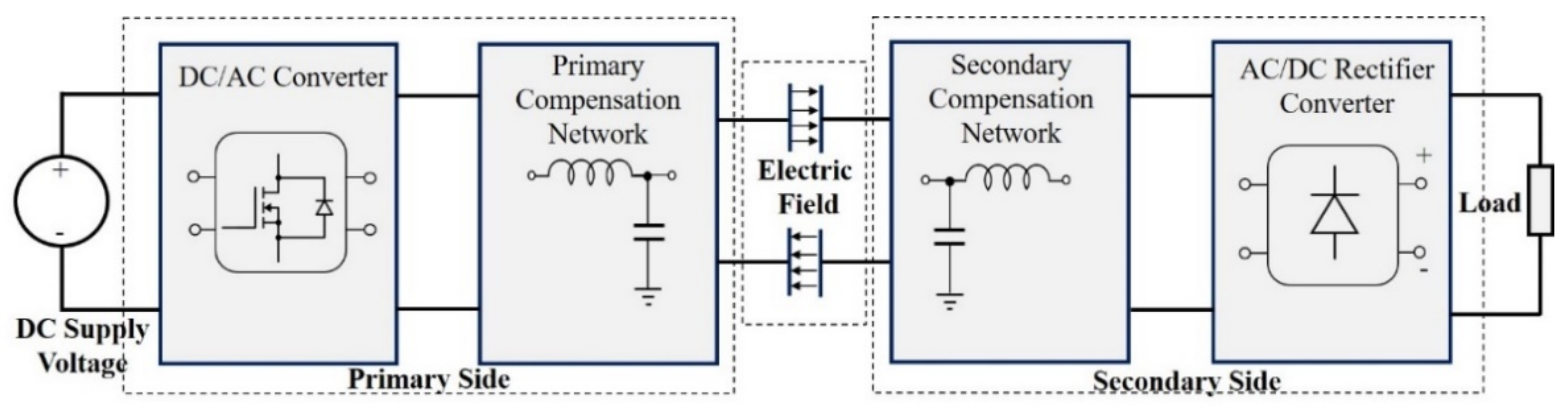
2. LC Compensated Capacitive Wireless Power Transfer System

The four-plate parallel structure, shown in Figure 2a, represents the most common solution to create air-coupled capacitors [9]. As shown in [34] and Figure 2a, plates P1 and P3 represent the primary side plates, while P2 and P4 are the secondary side plates. In general, the coupling between the plates Pi and Pj is modeled by a capacitance Cij. The couplings C12 and C34 are known as main capacitances, while C14, C23, C24, and C13 are called cross-coupling capacitances. Adopting the parallel structures shown in Figure 2a and assuming that the plates P1 and P2 are distant enough from P3 and P4 the cross-coupling capacitances can be neglected, making the analysis of the circuit easier. The analysis proposed in this paper is valid for any four-plate architecture system; therefore, even the cross-coupling capacitances are taken into account. By applying the Kirchhoff voltage law (KVL) and the Kirchhoff current law (KCL) to Figure 2a, it is possible to reconfigure the six-capacitance matrix into the equivalent π-topology circuit shown in Figure 2b, where
C M = C 24 C 13 C 14 C 23 C 13 + C 14 + C 23 + C 24
C A = C 12 + C 13 + C 14 C 23 + C 24 C 13 + C 14 + C 23 + C 24 C M
C B = C 34 + C 13 + C 23 C 14 + C 24 C 13 + C 14 + C 23 + C 24 C M
The plates being coupled through the air, the values of these capacitances usually are of few pF; thus, a high operating frequency must be used. To transfer the desired power to the load at any frequency, two external capacitances C1 and C2 are connected in parallel with CA and CB and must be designed to resonate with inductances L1 and L2 at an angular frequency ω0. The insertion of these two external capacitances produces two equivalent capacitances C1 = Cext1 + CA and C2 = Cext2 + CB, as shown in Figure 2b. To reduce the reactive power due to the low coupling between metal plates and increase the active output power, two external inductances L1 and L2 must be designed; to resonate with the capacitances C1 and C2, their values are derived as follows
L 1 = 1 ω 0 2 C 1
L 2 = 1 1 k c 1 ω 0 2 C 2
where kc is the coupling factor, and it is expressed as
k c = C M C 1 C 2
Being C1 >> CM and C2 >> CM, the coupling coefficient kc ≅ 0.

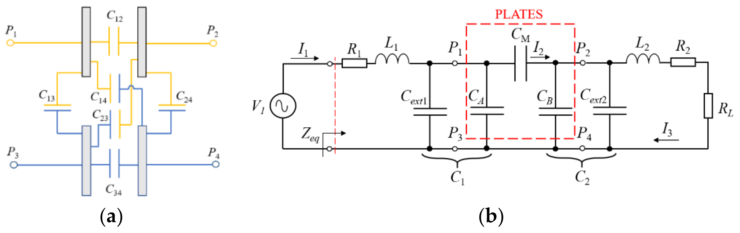
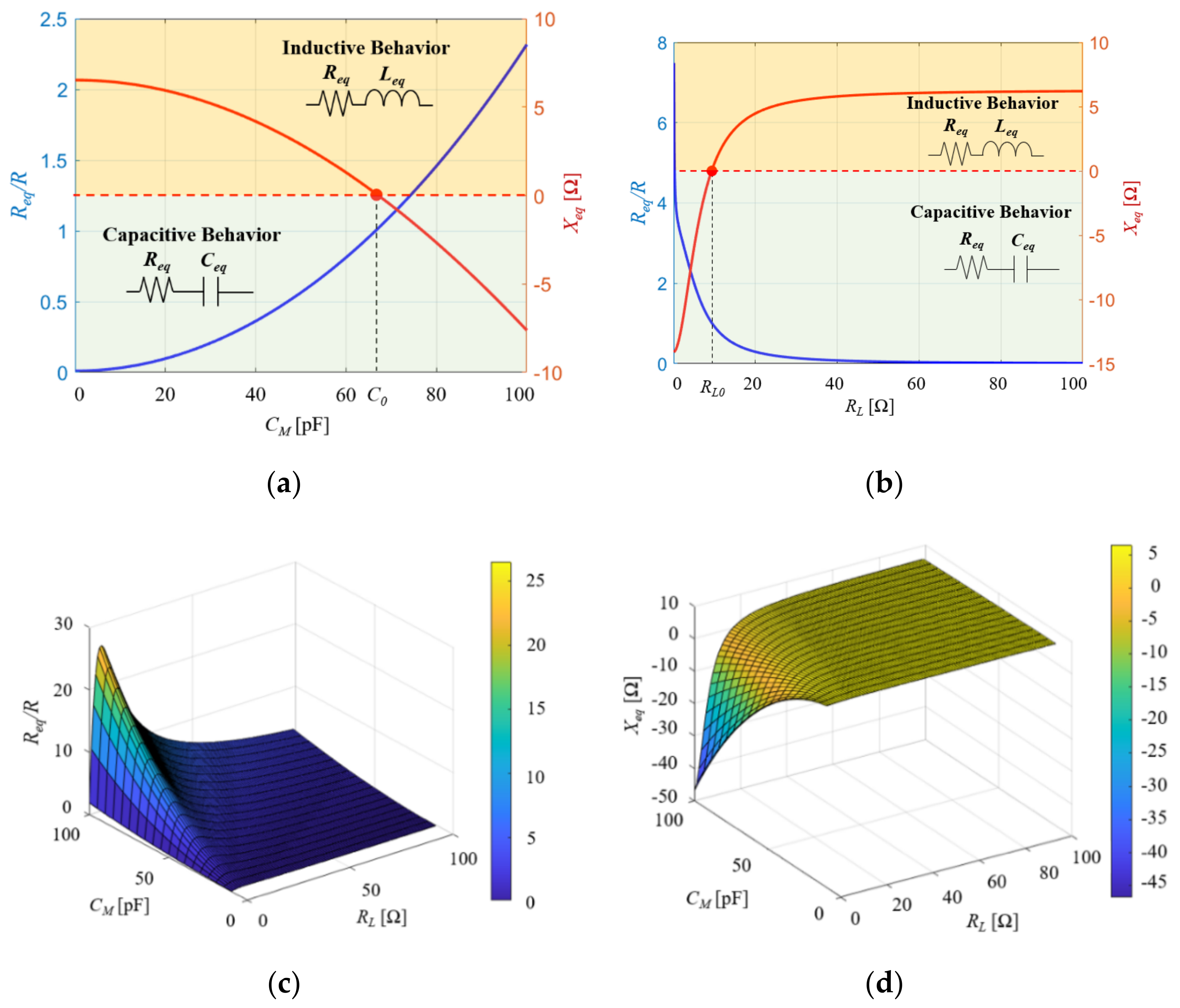
2.1. Equivalent Impedance

The knowledge of the equivalent impedance of the CWPT is crucial to achieve ZVS. Usually, the external capacitances are higher than the cross-capacitance, thus C1 = Cext1 + CACext1 and C2 = Cext2 + CBCext2. The geometry of the plates is symmetrical resulting in R1 = R2 = R, L1 = L2 = L and C1 = C2 = C; the equivalent impedance is
Z e q = 1 + ω 2 α R β ω 2 L 2 2 L C + j ω R + β C + α ω 2 L α β ω 2 + j ω C α ω 2 L
where α = CM2C1C2 and β = R + RL. The impedance Zeq = Req + j Xeq real and imaginary parts are
R e q = α β 1 + ω 2 α R β ω 2 L 2 2 L C + R + β C + ω 2 L α 2 ω 2 α 2 β 2 + C + ω 2 L α 2
X e q = C + ω 2 L α α ω 2 R + β 1 ω 2 α R β ω 2 L 2 2 L C ω ω 2 α 2 β 2 + C + ω 2 L α 2
The sign of the reactive part Xeq changes depending on the value of the coupling capacitance CM. The value of CM resulting in Xeq = 0 Ω is
C 0 = C 2 + 1 2 ω 2 L C ω 2 β 2 + ω 2 L 2
If CM < C0, the reactance Xeq > 0 Ω and the equivalent impedance is resistive–inductive with
L e q = X e q ω O = C + α ω 2 L α ω 2 R + β 1 ω 2 α R β ω 2 L 2 2 L C ω 2 α 2 β 2 ω 2 + C + α ω 2 L 2
On the other hand, CM > C0 results in Xeq < 0 Ω and the equivalent impedance is resistive–capacitive with
C e q = 1 ω O X e q = C + α ω 2 L 2 + α 2 β 2 ω 2 C + α ω 2 L α ω 2 R + β 1 ω 2 α R β ω 2 L 2 2 L C
The blue trace in Figure 3a represents the ratio between the equivalent resistance Req and the load resistance RL, while the red trace represents the reactance Xeq for different values of capacitive coupling CM. In Figure 3b, the ratio is between the equivalent resistance Req and the load resistance RL, while the red trace represents the reactance Xeq for different values of load resistance RL. In Figure 3c, the variation of Req/R under both coupling and load resistance variation is shown, while in Figure 3d, the 3D plot of the reactive part Xeq for different coupling and load resistance is shown.

2.2. Efficiency and Output Power

The efficiency is calculated as
η = P o P o + P i n = R L R L + R 2 + R 1 I 1 I 3 2
where the ratio between the input and output currents is expressed by applying the KVL and KCL to the circuit of Figure 2b as
I 1 I 3 = C M C β R e q R + ω L X e q + j ω L R e q R β X e q R e q R 2 + X e q 2
Assuming that the CWPT operates at the resonance, (14) simplifies as
I 1 I 3 2 = C M 2 C 2 β 2 + ω 2 L 2 R e q R 2 + X e q 2
Thus, the transmission efficiency is
η = R L β C 2 R e q R 2 + X e q 2 + R 1 C M 2 β 2 + ω 2 L 2
and the output current is expressed as
I 3 = C M C M R L + j ω β R C 2 C M 2
leading to an output power given by
P o = V i 2 C M 2 R L R L C M 2 + ω β R C 2 C M 2 2

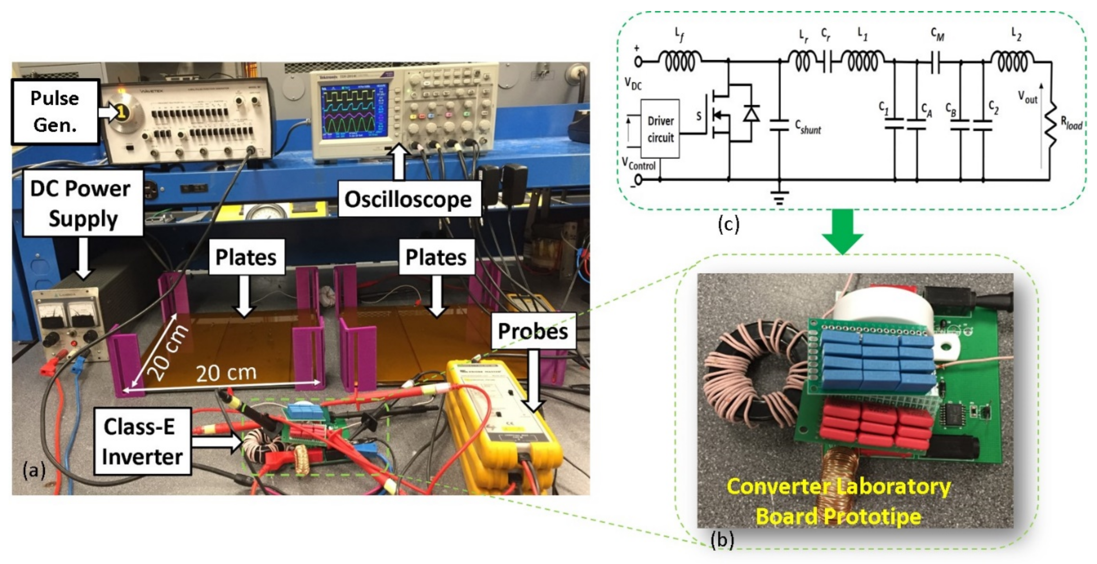
3. CWPT Class-E Inverter Circuit Analysis

In this section, the integration of the CWPT system with the Class-E inverter is presented.

3.1. Assumptions

The analysis is derived according to the following assumptions.
  • The duty cycle D of the MOSFET is 0.5;
  • The MOSFET turns ON and OFF instantly;
  • The MOSFET ON-resistance is zero;
  • The MOSFET output capacitance is linear and frequency invariant;
  • The loaded quality factor QL of the resonant network is high enough such that the currents through the transformer windings are sinusoidal (e.g., QL > 7);
  • The choke inductance is large enough to neglect the input current ac component. The dc resistance of the choke inductor is ignored. The self-capacitance of the choke inductor is absorbed into the shunt capacitance of the MOSFET.

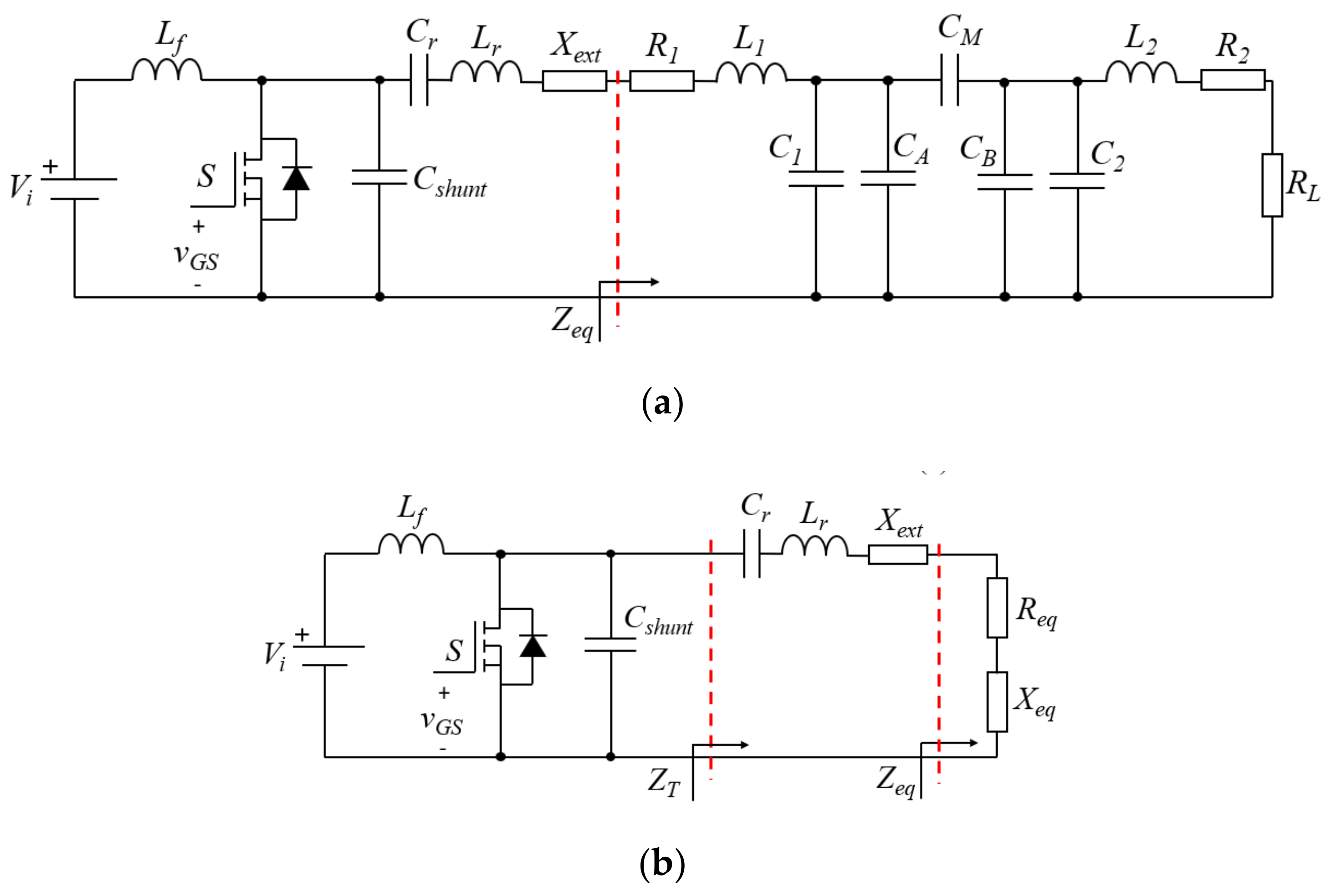
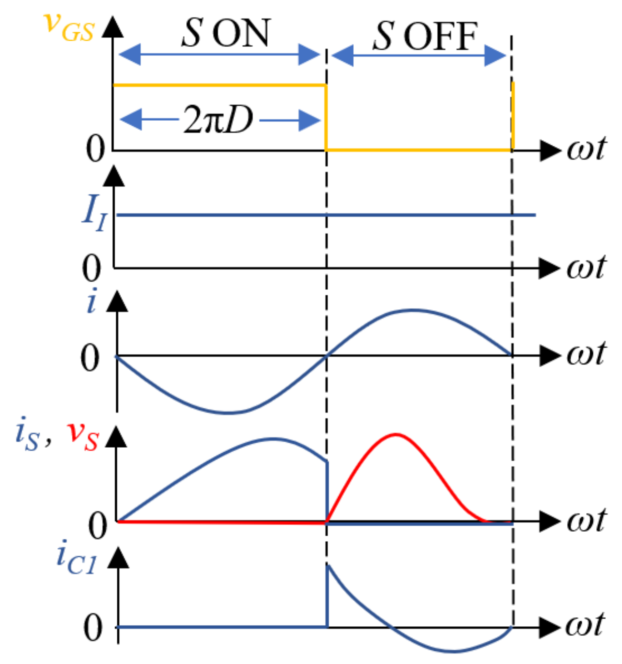
3.2. Circuit Descriptions

Figure 4a shows the Class-E DC–AC inverter for capacitive wireless power applications. Here, Vi is the DC supply voltage source, Lf is the choke inductor, S is the switch implemented by using a power MOSFET, and Cshunt is the voltage-shaping shunt capacitor across the switch. The power MOSFET output capacitance and the self-capacitance of the choke are included in the overall capacitance Cshunt connected in parallel with the switch.
In some applications, it is preferable to work at not excessively high frequencies, especially when the transferred power is high. Therefore, to integrate the CWPT into the Class-E inverter topology, it is necessary to add the capacitances C1 and C2 and the inductances L1 and L2, as shown in Figure 4a. The circuit can be represented in the basic topology of Figure 4b introducing the equivalent impedance of CWPT Zeq. Then, the components Cr and Lr, representing the resonant tank, can be properly tuned to achieve inductive load for soft-switching operation. The typical voltage and current waveforms of the circuit operating at ZVS/ZDS conditions are shown in Figure 5.

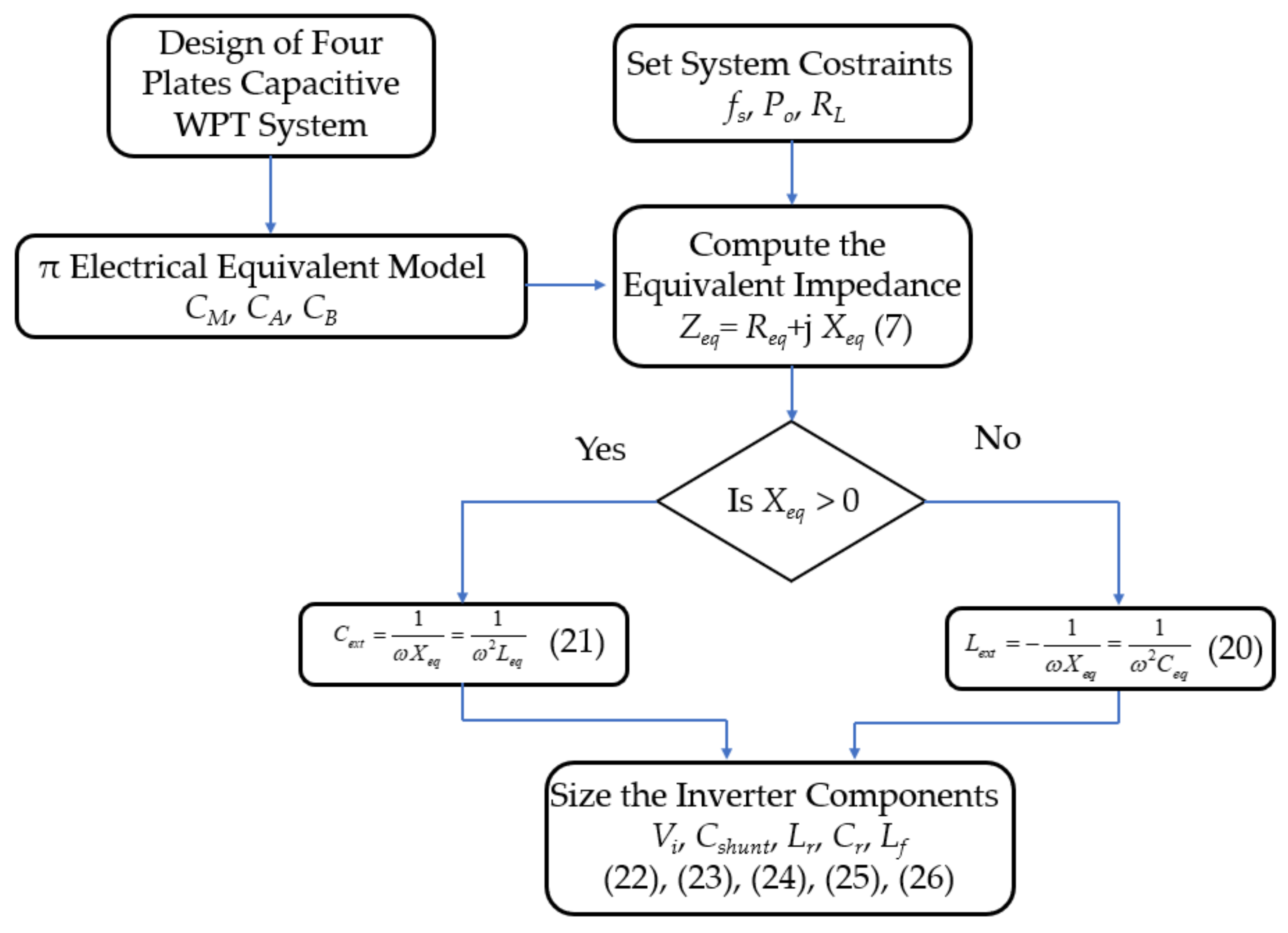
3.3. Optimum Design Procedure
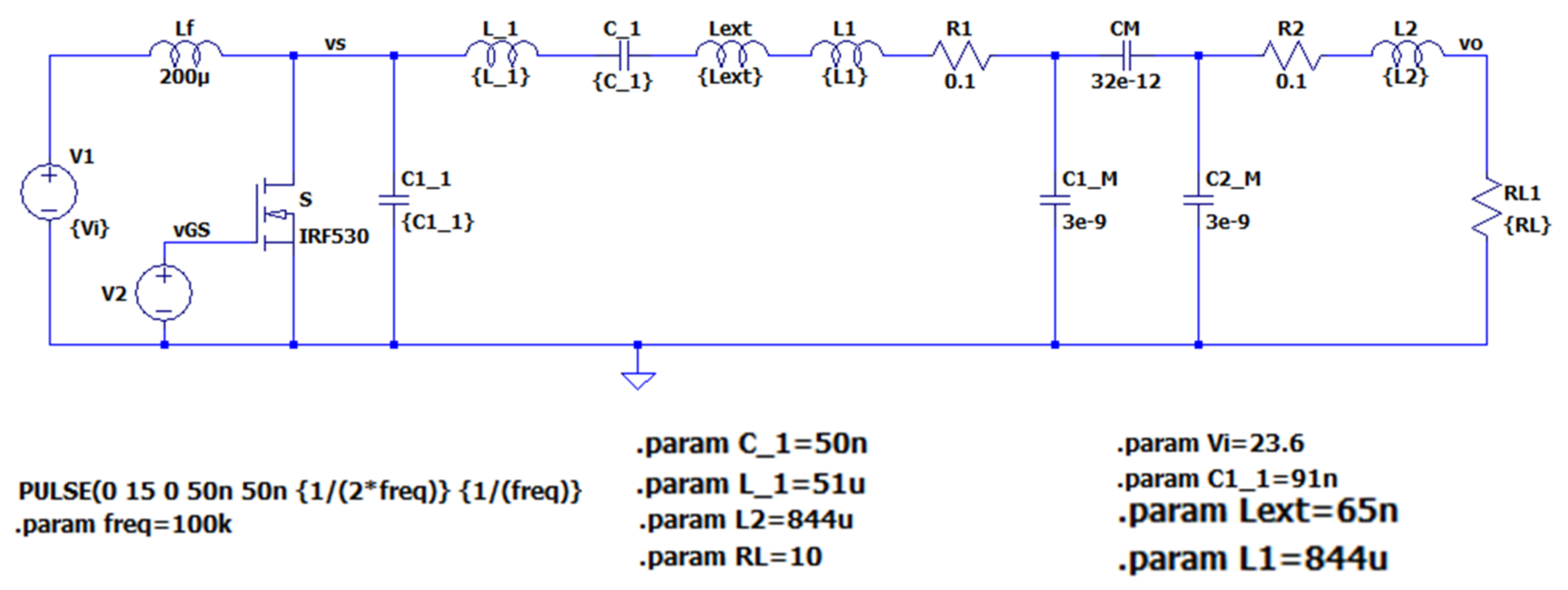
Figure 4b shows the DC–AC Inverter where the CWPT system is replaced by its equivalent impedance Zeq = Req + j Xeq. As discussed in the previous section, depending on the value of CM, the equivalent reactance results to be either inductive or capacitive, as shown in Figure 3b. Let us assume that the system is working at the switching frequency f = ω/(2π).
Depending on the application, an optimal value of coupling CMopt must be defined.
To reduce the current circulation, the reactive part of the equivalent impedance Xeq must be canceled by adding an external reactance Xext in series, leading to
X e x t = X e q .
In this way, when the system operates at CM = CMopt, the equivalent impedance of the CWPT system is purely resistive Zeq = Req. The external inductance, which must be series connected to the LC resonant tank when Xeq < 0 Ω to satisfy (19), is
L e x t = 1 ω X e q = 1 ω 2 C e q
When Xeq > 0 Ω, the external capacitance series-connected with the LC resonant tank to satisfy (19) is given by
C e x t = 1 ω X e q = 1 ω 2 L e q
Assuming that the load resistance RL, the operating frequency f0 = ω0/(2π), and the output power Po values are known as design specifications, the expressions for the components needed to reach the ZVS and ZDS condition at CM = CMopt are given by [35]
V i = π 2 + 4 8 P o R e q
C s h u n t = 8 π π 2 + 4 1 ω C 1 R e q
L r = Q L R e q ω
C r = 1 ω R e q Q L π π 2 4 16
Regarding the choke inductor, it can be calculated as [36]
L f = 14 π R e q ω
If the position of plates is not in the optimal position, the coupling is different from the nominal value CMopt, and therefore (19) is not satisfied. An in-depth analysis of the Class-E inverter under misalignment between plates is derived in Section 4.

3.4. Design Example

In this case of study, the considered power inverter has a nominal output power PO = 100 W, the load resistance is RL = 10 Ω, the operating frequency is f0 = 100 kHz, and the quality factor is selected to be QL = 10. The parasitic resistances are assumed to be R1 = R2 = 0.1 Ω.
The coupling capacitance is CM = 64 pF. It is assumed that CA and CB are much lower than the external capacitances C1 and C2. These capacitances are fixed as C1 = C2 = 3 nF. From (6), the coupling factor is kc = 0.023. Thus, the primary and secondary inductances are
L 1 = L 2 = 1 1 k c 1 ω 0 2 C = 844   μ H
From (8)–(20), the equivalent impedance is Zeq = Req + j Xeq = 3.2 − j0.0411, Xeq < 0, according to (11)–(21), so
C e q = 1 ω X e q = 38.7   μ F
L e x t = 1 ω 2 C e q = 65.4   nH
Finally, by using (22)–(26), the shunt capacitance, the resonant inductance, the resonant capacitor, and the choke inductance are calculated as Cshunt = 91 nF Lr = 51 µH, Cr = 56 nF, and Lf =200 µH, respectively.
The proposed design procedure is represented as a flowchart in Figure 6. Starting from the four plates capacitive wireless power transfer structure, the equivalent π electric circuit can be extrapolated. Defining the system characteristics, such as the operating frequency, the output power, and the load resistance, the equivalent impedance Zeq can be calculated. To cancel the reactive part Xeq, a capacitor Cext can be added if Xeq > 0.

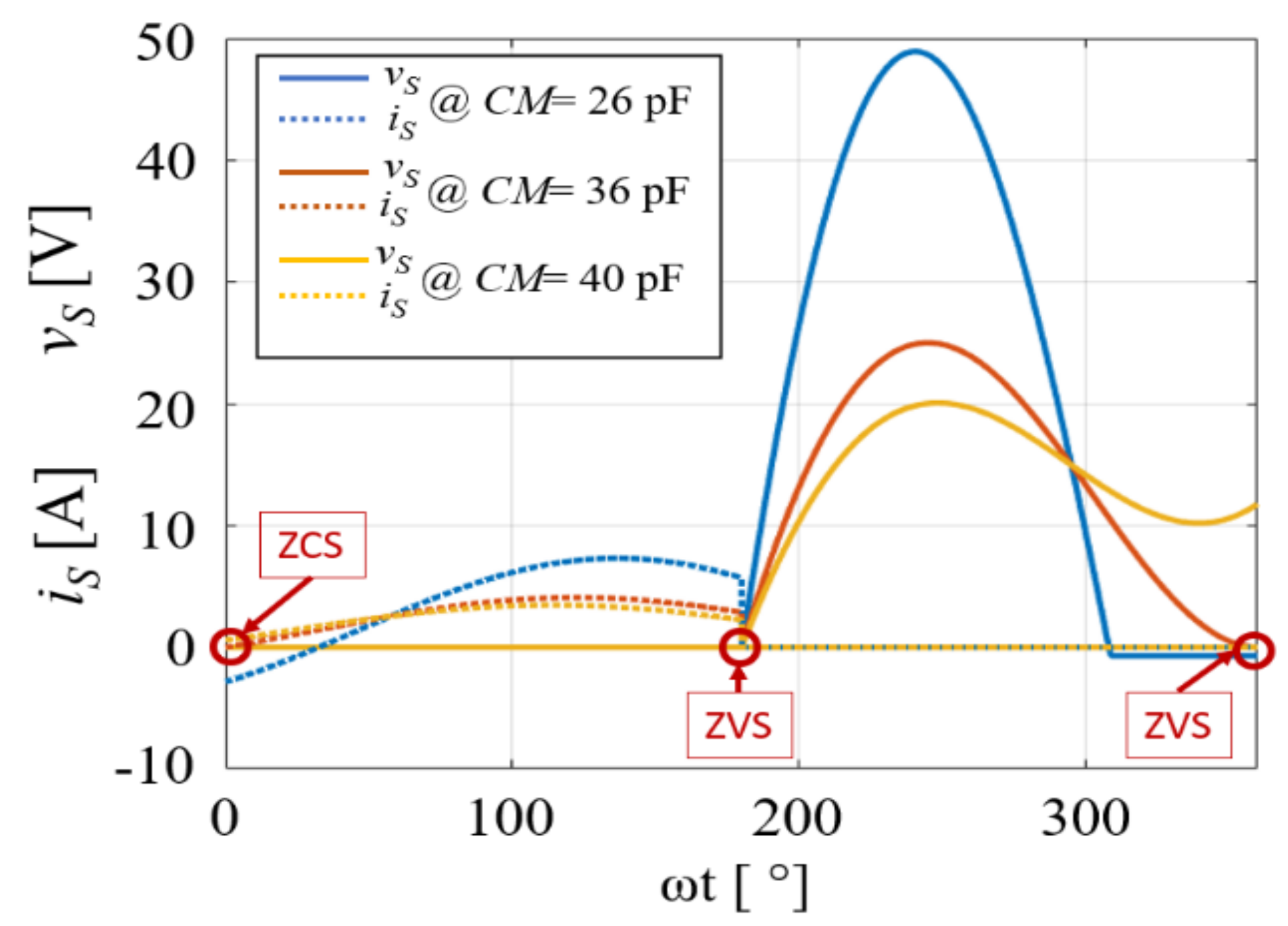
4. Class-E Inverter Behavior at Any Coupling Coefficient

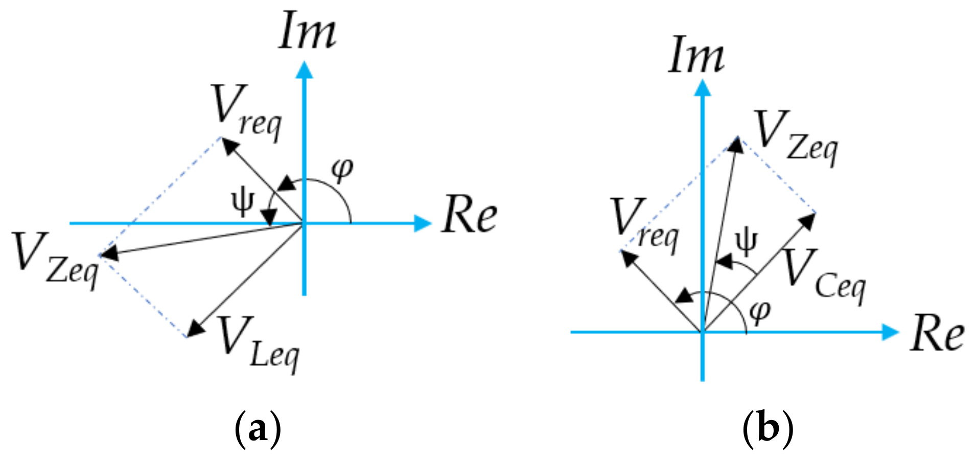
4.1. Analytical Model

In this section, the analytical expressions of current and voltage waveforms across the components are derived. According to Figure 4, an equivalent impedance ZT = RT + j XT can be defined; its phase is
ψ = arctan R T X T
The current through the series-resonant circuit is sinusoidal and given by
i = I m sin ω t + φ
where Im is the amplitude, and φ is the initial phase. The vector relationship between the angle ψ and φ is shown in Figure 7. If XT > 0 Ω, the voltage across the equivalent inductance VLT leads by 90° the voltage across the equivalent resistance VRT, as shown in Figure 7a; while if XT < 0 Ω, voltage VRT leads by 90° voltage VCT, as shown in Figure 7b.
If the impedance is resistive–inductive, the first harmonic of the voltage v1shunt applied to ZT can be split into the voltage across the equivalent resistance RT and that across the equivalent reactance XT.
v s h u n t 1 ( ω t ) = v R t ( t ) + v L t ( t ) = V R t sin ( ω t + φ ) + V L t cos ( ω t + φ )
Using (31), the relationship between the angles ψ and φ, at a fixed duty cycle is derived as
tan ( ψ ) = π 2 + 2 cos ψ cos ( 2 π D + ψ ) + cos ( 2 π D + ψ ) 1 4 sin π D + ψ cos ( π D + ψ )
This relationship is also shown in Figure 8, for three different values of the duty cycle.
The drain to source voltage across the MOSFET is
v s ( ω t ) = 1 C 1 2 π D ω t i C 1 d ω t = 0 0 < ω t < 2 π D 1 ω C 1 I I ω t 2 π D + I m cos ( ω t + φ ) cos ( 2 π D + φ ) 2 π D < ω t < 2 π
If the choke inductance Lf is big enough to assume the input current II to be constant, the input voltage VI can be calculated as the average value of the vs
V i = 1 2 π 2 π D 2 π v s d ω t = 1 2 π 2 π D 2 π 1 ω C 1 I i ω t 2 π D + I m cos ( ω t + φ ) cos ( 2 π D + φ ) d ω t = = 1 2 π ω C 1 2 π I i 1 D 2 + I m sin φ 1 cos 2 π D sin 2 π D cos φ 2 π 1 D cos 2 π D + φ
Under the assumptions used for this analysis, the power losses for the circuit can be neglected. This means that Po = Vo Io and Pi = Vi Ii. Thus, the amplitude of the current through the resonant tank can be expressed as
I m = 2 π ω V i 2 π 2 I i 1 D 2 sin φ 1 cos 2 π D sin 2 π D cos φ 2 π 1 D cos 2 π D + φ

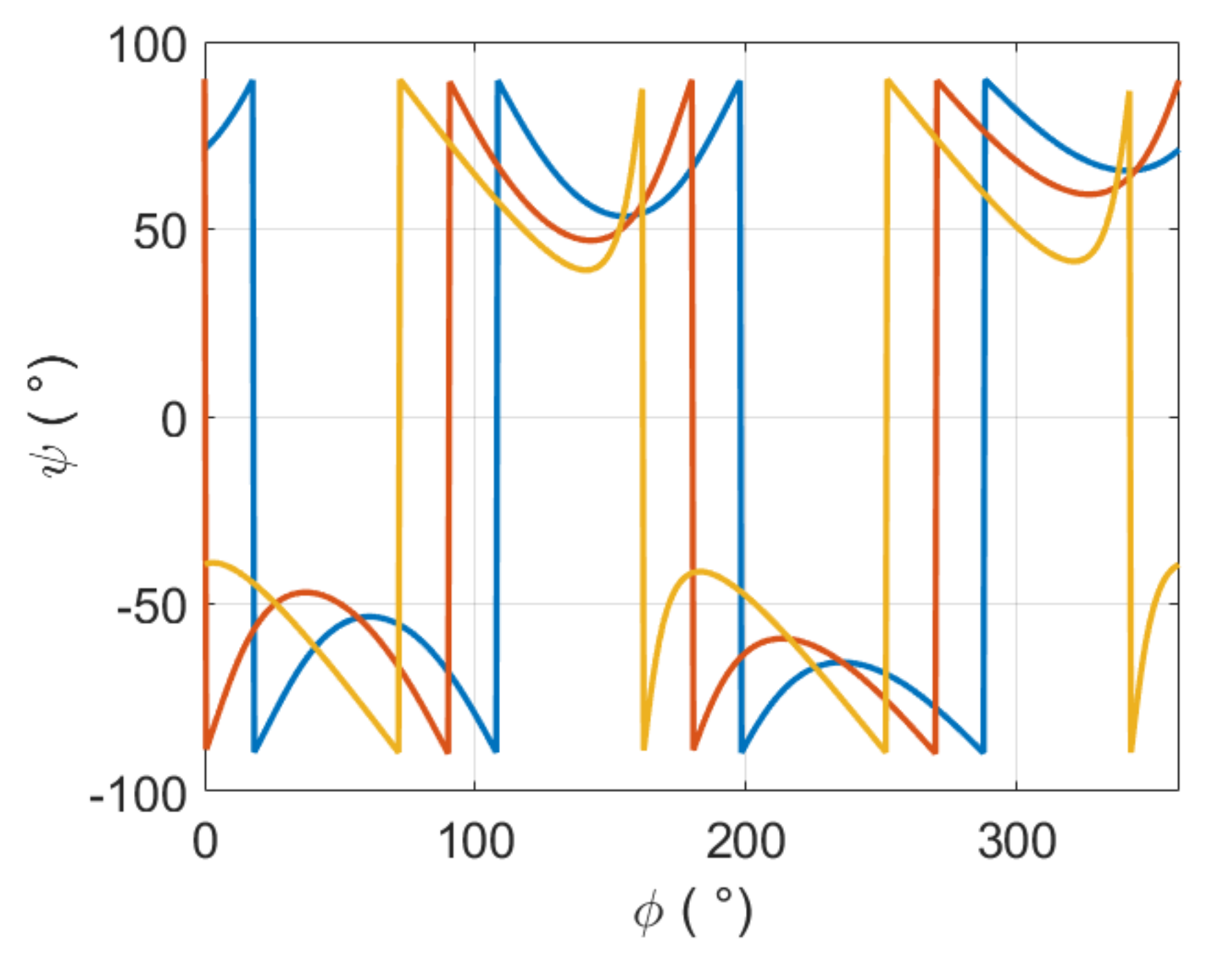
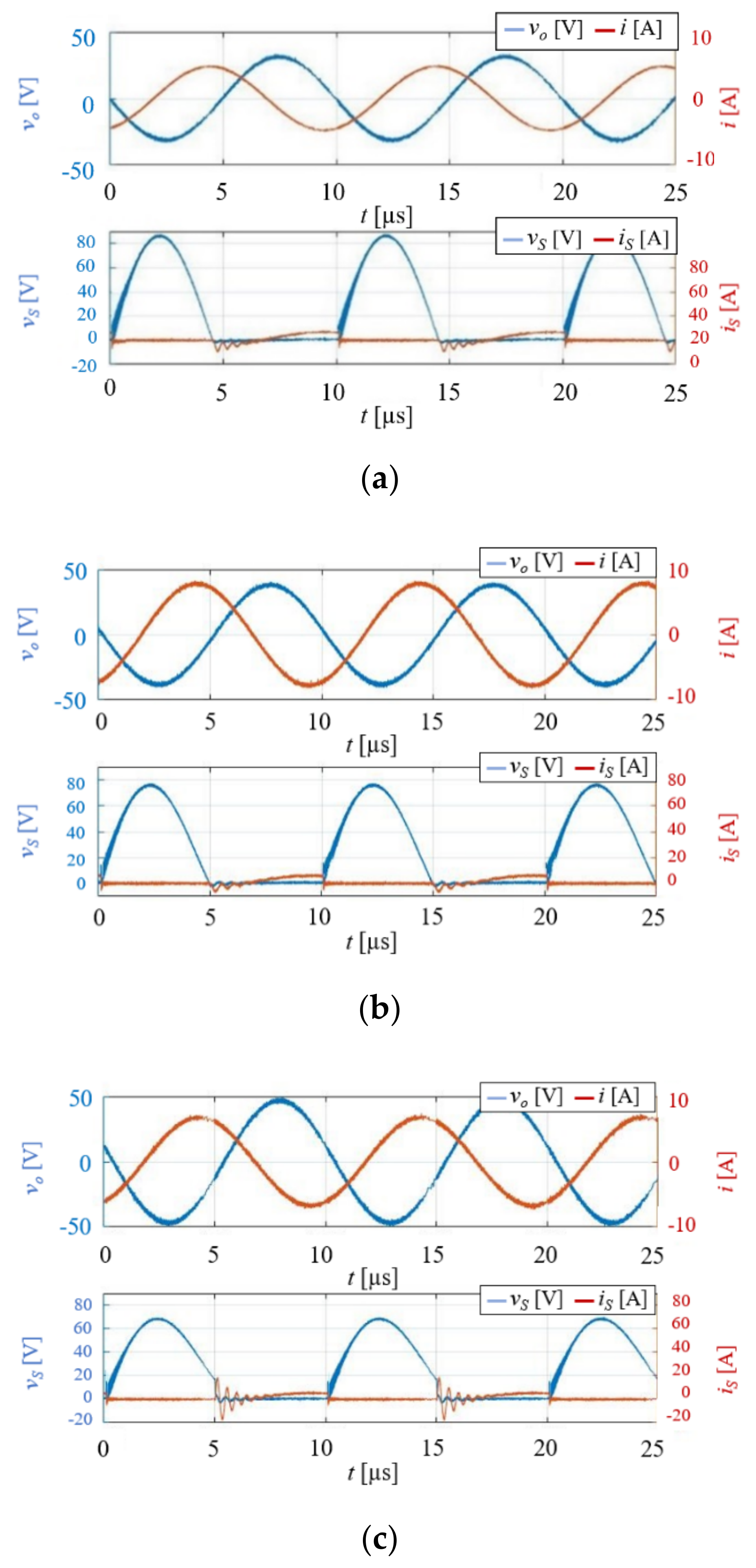
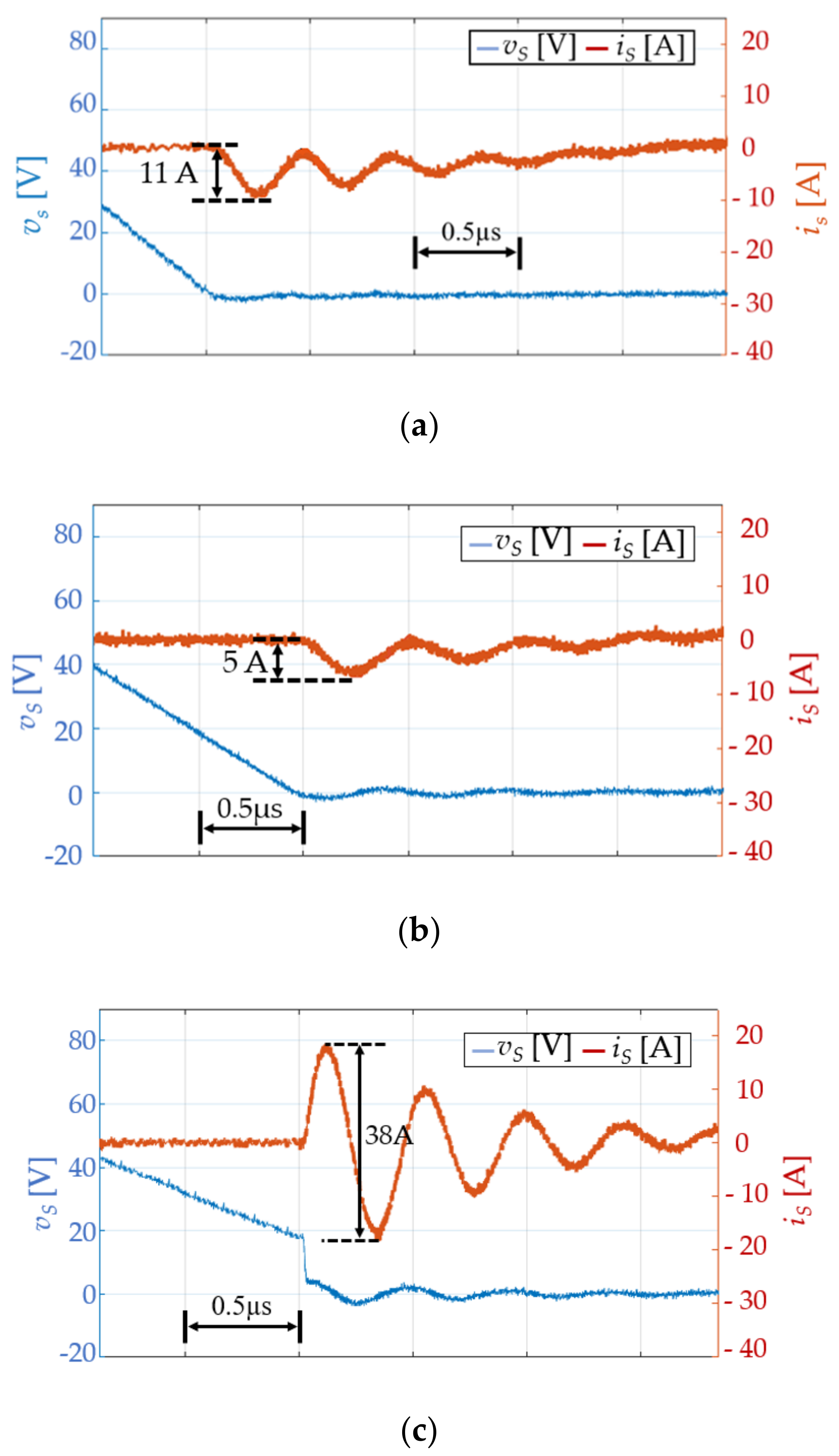
4.2. Voltage and Current Waveforms

The equations shown in the previous section allow the study of the system behavior under capacitive coupling changes. Using (34) and (36), the voltage and the current through the MOSFET for three different values of coupling capacitance CM were calculated. The waveforms computed using the previous equations using the nominal values summarized in Table 1 are shown in Figure 9.
The dotted lines in Figure 9 represent the current through the MOSFET is, while the continuous line is the drain to source voltage vs. Note that the ZVS/ZDS condition is achieved only for the optimum value of coupling capacitance CMopt = 32 pF. When the plates are strayed leading to a lower coupling capacitance CM < CMopt, the ZVS condition is still achieved, as shown for CM = 25 pF. When CM = CMopt, at ωt = 0 both ZCS and ZVS are reached, being both the current and the voltage across the MOSFET zero, while, when ωt =180°, only ZVS is achieved, being the current different from zero. When the plates come closer with respect to the optimum position CM > CMopt, the ZCS condition is not achieved at ωt = 0, while it is almost achieved CM < CMopt.

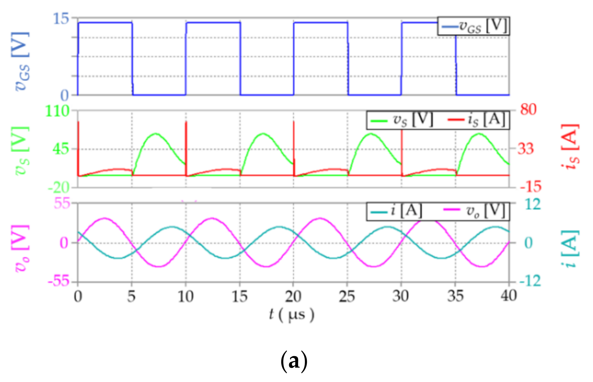
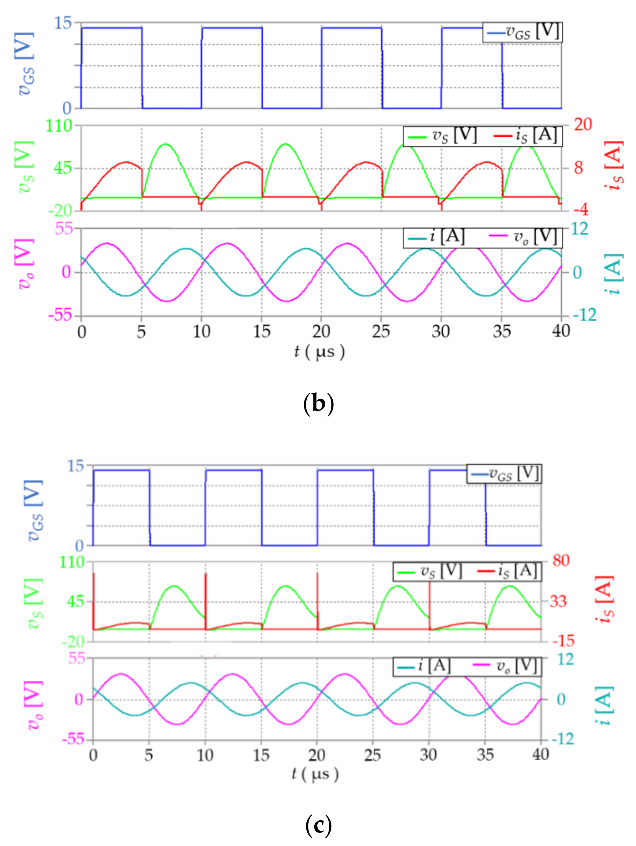
5. Simulation and Experimental Results

To validate the analysis results obtained using the analytical equations, the circuit was implemented in LTSpice and validated experimentally.

5.1. Simulations

The results obtained by using the analytical model described in the previous section are here validated through simulations. The circuit is implemented in LTSpice as shown in Figure 10 with the values component values shown in Table 1. To evaluate the effects of misalignment, three different values of coupling capacitance CM were studied. Figure 11a shows the current and voltage waveforms resulting at CM = 25 pF. The power delivered to the load is reduced to Po = 89 W, and also the efficiency reduces to η = 0.91. In Figure 11b, the case with CM = CMopt = 32 pF is considered, both ZVS and ZDS are achieved, the output power is Po = 92 W, and the system efficiency is η = 0.95. Finally, the circuit with CM = 45 pF is simulated, ZVS condition is not achieved, and the transmitted power increases to Po = 95 W, but the converter efficiency further decreases to η = 0.89, as shown in Figure 11c. Note that at CM = 25, pF ZVS is still achieved, but the voltage stress across the MOSFET significantly increases if compared with the other couplings.

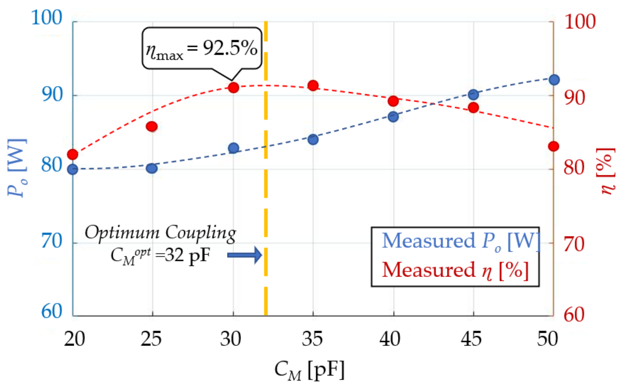
5.2. Experimental Results

To validate the simulations, a power converter experimental circuit has been realized. A picture of the experimental setup is shown in Figure 12a. An enlargement of the PCB board is shown in Figure 12b, while the equivalent electric circuit is shown in Figure 12c. The four plates are steel made. The measured values and the component parasitic resistances are given in Table 2. The inductance was made by using AWG40 Litz wire to reduce the parasitic resistance at fs = 100 kHz. A Silicon Super Junction MOSFET-R6020JNJ is used [37]. The main MOSFET parameters are reported in Table 3.
The experimental tests were performed under three different values of CM. Figure 13a shows the waveforms at CM = 25 pF. The amplitude of the LC resonant current is I = 8.9 A, the output voltage is Vo = 39.8 V, and the output power Po = 80 W with a transmission efficiency η = 82.4%. In Figure 13b, the measured waveforms at CM = CMopt = 32 pF are shown. The waveforms of the current flowing into the LC resonant tank i and that of the voltage across the load resistance vo are perfectly sinusoidal with amplitudes of I = 8.3 A and Vo = 28.9 V, respectively.
The measured transmission efficiency is η = 92.5%. Finally, in Figure 13c, the waveforms at CM = 45 pF are shown. The current flowing through the resonant tank stays approximately constant to I = 8.3 A, but the voltage across the load is Vo = 47.8 V, the transmitted power Po = 90.6 W, and a transmission efficiency η = 88.5%. Concerning the achievement of the ZVS condition, it can be seen that for CM = 25 pF, the ZVS condition is still achieved, but the voltage stress across the MOSFET is increased reaching a maximum voltage VDSmax ≅ 90 V.
Operating with CM = CMopt = 32 pF, both the ZVS/ZDS conditions are achieved, while when the coupling increases as for CM = 45 pF, the ZVS condition is not achieved anymore, leading to ringing and switching power losses.
The converter also results in a very low output voltage total harmonic distortion (THD) as shown in Table 4, where the DC component and the THD of the output voltage for the three different capacitive couplings are summarized.
Although the conversion efficiency is highly sensitive to coupling variation, the THD of the output voltage is also very low when the converter operates outside the optimum coupling.
An enlargement of the turn-on switching voltage and current waveforms for the three coupling cases is shown in Figure 14. The blue trace represents the voltage across the MOSFET vS, while the red trace represents the current iS. It can be seen that for both the cases, CM = 25 pF and CM = 32 pF ZVS is achieved, while for CM = 45 pF, the ZVS condition is not achieved, and a higher current oscillation occurs after the turn-on, thus leading to higher switching losses.
The experimental results confirm both the analysis and simulation results. Mutual capacitance CM is one of the key parameters to investigate to achieve the ZVS and ZDS operations. The same transient behavior obtained from analytical equations and simulations is highlighted. When plates are moved from the optimal position, ZVS is still reached, but the power is transferred to the load, and the efficiency decreases. On the other hand, when the plates are placed at a closer distance than that of the optimal position, the transferred power increases, but the ZVS is not achieved, leading to a lower transmission efficiency. The abovementioned behavior of the converter versus coupling capacitance CM is illustrated in Figure 15, where the experimentally measured output power and conversion efficiency are shown. The maximum DC–AC conversion efficiency occurs at the optimum coupling capacitance CMopt. This is due to the achievement of the ZVD/ZDS condition, which drastically reduces the MOSFET switching losses, while the conduction losses are mainly related to the switch current root mean square (RMS) is,rms (Figure 9) and the RDS,ON of the chosen device [38,39]. Figure 15 also shows that the transferred power increases if the plate coupling increases.
In Table 5, the comparison in terms of output power, efficiency, operating frequency, and capacitive coupling between Class-E circuits available in the literature is shown.
As shown, the proposed solution allows the increase of the transferred power operating at reduced switching frequency despite the low capacitive coupling.

6. Conclusions

This paper presents a complete analysis and the design procedure of the CWPT system based on a Class-E inverter. The analysis is focused on the coupling capacitance and its effects on the design constraints. It has been shown that the inverter satisfies both ZVS and ZDS conditions at a selected optimum coupling capacitance CMopt and satisfies ZVS conditions for 0 < CM < CMopt, yielding a high conversion efficiency. The expressions for the inverter current and voltages have been determined as functions of the coupling capacitance CM, so that the converter behavior also under misalignment between plates is predicted. Simulations and experimental results have been provided to validate the theoretical derivations.
Using the results of this paper, CWPT Class-E inverters can be designed for applications with fixed or variable coupling coefficient at any fixed load impedance. Additionally, thanks to the LC compensation, the operation at a lower frequency is allowed. This feature is obtained through a simpler control strategy with reduced switching losses and high quality of output waveforms (low THD). Therefore, compared with the similar experimental setup available in the literature, the proposed system is characterized by a higher output power transfer and a lower switching frequency.
Lower switching frequency operation allows controlling the system using controllers with low computational capabilities, which can be a useful feature for low-cost applications.
Furthermore, it operates at a lower frequency, leading to core losses reduction. On the other hand, this solution is useful for those applications where the optimization of the dimension and weight of the inverter is not of primary importance.
Practical applications of the considered CWPT circuit are in a wide variety of areas, including wireless power charging, induction heating, wireless-charged biomedical transplants, DC–DC power conversion, and DC–AC power inversion.
As future development, the performance of the DC–AC inverter using different four plates structures will be evaluated. A comparison between different structure solutions in terms of horizontal and vertical misalignment will be studied. Additionally, an extensive analysis of the power losses in the circuit will be evaluated, placing attention on the MOSFET losses and the losses due to parasitic components.

Author Contributions

Conceptualization: Y.-H.W., F.C., A.R., S.M., and D.C.; validation: Y.-H.W., and F.C.; writing–original draft preparation: F.C.; writing–review and editing: F.C., A.R., and S.M.; visualization: Y.-H.W., F.C., A.R., S.M., and D.C.; supervision: A.R., S.M., and D.C.; project administration: Y.-H.W., F.C., A.R., S.M., and D.C. All authors have read and agreed to the published version of the manuscript.

Funding

This work was supported by the Ministry of Science and Technology of Taiwan, R.O.C. with grant number MOST-108-2221-E-606-015.

Institutional Review Board Statement

Not applicable.

Informed Consent Statement

Informed consent was obtained from all subjects involved in the study.

Data Availability Statement

Conceptualization, Y.W., F.C., A.R., S.M., and D.C.; validation, Y.W., F.C.; writing–original draft preparation, F.C.; writing–review and editing, F.C., A.R., and S.M.; visualization, Y.W., F.C., A.R., S.M. and D.C..; supervision, A.R., S.M. and D.C.; project administration, Y.W., F.C., A.R., S.M., and D.C. All authors have read and agreed to the published version of the manuscript.

Conflicts of Interest

The authors declare no conflict of interest.

References

  1. Schormans, M.; Valente, V.; Demosthenous, A. Correction to Practical Inductive Link Design for Biomedical Wireless Power Transfer: A Tutorial. IEEE Trans. Biomed. Circuits Syst. 2019, 13, 592. [Google Scholar] [CrossRef] [PubMed]
  2. Covic, G.A.; Boys, J.T. Modern Trends in Inductive Power Transfer for Transportation Applications. IEEE J. Emerg. Sel. Top. Power Electron. 2013, 1, 28–41. [Google Scholar] [CrossRef]
  3. Corti, F.; Reatti, A.; Pierini, M.; Barbieri, R.; Berzi, L.; Nepote, A.; De La Pierre, P. A Low-Cost Secondary-Side Controlled Electric Vehicle Wireless Charging System using a Full-Active Rectifier. In Proceedings of the 2018 International Conference of Electrical and Electronic Technologies for Automotive, Milan, Italy, 9–11 July 2018; pp. 1–6. [Google Scholar]
  4. Carobolante, F.; Menegoli, P.; Marino, F.A.; Jeong, N.S. A Novel Charger Architecture for Resonant Wireless Power Transfer. IEEE J. Emerg. Sel. Top. Power Electron. 2018, 6, 571–580. [Google Scholar] [CrossRef]
  5. Zaman, H.U.; Islam, T.; Hasan, K.S.; Antora, R.K. Mobile phone to mobile phone wireless power transfer. In Proceedings of the 2015 International Conference on Advances in Electrical Engineering (ICAEE), Dhaka, Bangladesh, 17–19 December 2015; pp. 206–209. [Google Scholar]
  6. Liu, Y.; Li, B.; Huang, M.; Chen, Z.; Zhang, X. An Overview of Regulation Topologies in Resonant Wireless Power Transfer Systems for Consumer Electronics or Bio-Implants. Energies 2018, 11, 1737. [Google Scholar] [CrossRef] [Green Version]
  7. Tampubolon, M.; Pamungkas, L.; Chiu, H.-J.; Liu, Y.-C.; Hsieh, Y. Dynamic Wireless Power Transfer for Logistic Robots. Energies 2018, 11, 527. [Google Scholar] [CrossRef] [Green Version]
  8. Xie, L.; Shi, Y.; Hou, Y.T.; Lou, A. Wireless power transfer and applications to sensor networks. IEEE Wirel. Commun. 2013, 20, 140–145. [Google Scholar] [CrossRef]
  9. Bartolini, A.; Corti, F.; Reatti, A.; Ciani, L.; Grasso, F.; Kazimierczuk, M.K. Analysis and Design of Stand-Alone Photovoltaic System for precision agriculture network of sensors. In Proceedings of the 2020 IEEE International Conference on Environment and Electrical Engineering and 2020 IEEE Industrial and Commercial Power Systems Europe (EEEIC/I&CPS Europe), Madrid, Spain, 9–12 June 2020; pp. 1–5. [Google Scholar]
  10. Hui, S.Y.R.; Zhong, W.; Lee, C.K. A Critical Review of Recent Progress in Mid-Range Wireless Power Transfer. IEEE Trans. Power Electron. 2014, 29, 4500–4511. [Google Scholar] [CrossRef] [Green Version]
  11. Dai, J.; Ludois, D.C. A Survey of Wireless Power Transfer and a Critical Comparison of Inductive and Capacitive Coupling for Small Gap Applications. IEEE Trans. Power Electron. 2015, 30, 6017–6029. [Google Scholar] [CrossRef]
  12. Minnaert, B.; Stevens, N. Maximizing the Power Transfer for a Mixed Inductive and Capacitive Wireless Power Transfer System. In Proceedings of the 2018 IEEE Wireless Power Transfer Conference (WPTC), Montreal, QC, Canada, 3–7 June 2018; pp. 1–4. [Google Scholar]
  13. Yi, K. Capacitive Coupling Wireless Power Transfer with Quasi-LLC Resonant Converter Using Electric Vehicles’ Windows. Electronics 2020, 9, 676. [Google Scholar] [CrossRef] [Green Version]
  14. Funato, H.; Kobayashi, H.; Kitabayashi, T. Analysis of transfer power of capacitive power transfer system. In Proceedings of the 2013 IEEE 10th International Conference on Power Electronics and Drive Systems (PEDS), Kitakyushu, Japan, 22–25 April 2013; pp. 1015–1020. [Google Scholar]
  15. Mazli, M.S.; Fauzi, W.N.N.W.; Khan, S.; Aznan, K.A.; Nataraj, C.; Adam, I.; Kadir, K.; Ahmed, M.M.; Yaacob, M. Inductive & Capacitive Wireless Power Transfer System. In Proceedings of the 2018 7th International Conference on Computer and Communication Engineering (ICCCE), Kuala Lumpur, Malaysia, 19–20 September 2018; pp. 307–312. [Google Scholar]
  16. Pagano, R.; Abedinpour, S.; Raciti, A.; Musumeci, S. Efficiency optimization of an integrated wireless power transfer system by a genetic algorithm. In Proceedings of the 2016 IEEE Applied Power Electronics Conference and Exposition (APEC), Long Beach, CA, USA, 20–24 March 2016; pp. 3669–3676. [Google Scholar]
  17. Pagano, R.; Abedinpour, S.; Raciti, A.; Musumeci, S. Modeling of planar coils for wireless power transfer systems including substrate effects. In Proceedings of the IECON 2016—42nd Annual Conference of the IEEE Industrial Electronics Society, Florence, Italy, 23–26 October 2016; pp. 1129–1136. [Google Scholar]
  18. Shenai, K. Future Prospects of Widebandgap (WBG) Semiconductor Power Switching Devices. IEEE Trans. Electron Devices 2014, 62, 248–257. [Google Scholar] [CrossRef]
  19. Liu, K.-H.; Lee, F. Zero-voltage switching technique in DC/DC converters. IEEE Trans. Power Electron. 1990, 5, 293–304. [Google Scholar] [CrossRef]
  20. Ogi, Y.; Ebihara, F.; Wei, X.; Sekiya, H. A Novel Circuit Topology and Its Design for Class-E2 DC-DC Converter. In Proceedings of the 2019 IEEE Energy Conversion Congress and Exposition (ECCE), Baltimore, MD, USA, 29 September–3 October 2019; pp. 1256–1260. [Google Scholar]
  21. Aldhaher, S.; Luk, P.C.; Bati, A.F.; Whidborne, J.F. Wireless Power Transfer Using Class E Inverter With Saturable DC-Feed Inductor. IEEE Trans. Ind. Appl. 2014, 50, 2710–2718. [Google Scholar] [CrossRef] [Green Version]
  22. Li, Y.-F.; Sue, S.-M. Exactly analysis of ZVS behavior for class E inverter with resonant components varying. In Proceedings of the 2011 6th IEEE Conference on Industrial Electronics and Applications, Beijing, China, 21–23 June 2011; pp. 1245–1250. [Google Scholar]
  23. Dong, G.; Liangzong, H.; Bing, C.; Han, G. An Active Clamping Strategy for Class-E Inverter in Wireless Power Transfer System. In Proceedings of the 2019 IEEE International Symposium on Predictive Control of Electrical Drives and Power Electronics (PRECEDE), Quanzhou, China, 1 May–2 June 2019; pp. 1–5. [Google Scholar] [CrossRef]
  24. Ahmad, S.; Muharam, A.; Hattori, R. Rotary Capacitive Power Transfer with Class-E Inverter And Balun Circuit. In Proceedings of the 2020 IEEE PELS Workshop on Emerging Technologies: Wireless Power Transfer (WoW), Seoul, Korea, 15–19 November 2020; pp. 330–333. [Google Scholar]
  25. Ueda, H.; Koizumi, H. Class-E2 DC-DC Converter With Basic Class-E Inverter and Class-E ZCS Rectifier for Capacitive Power Transfer. IEEE Trans. Circuits Syst. II Express Briefs 2020, 67, 941–945. [Google Scholar] [CrossRef]
  26. Chokkalingam, B.; Padmanaban, S.; Leonowicz, Z.M. Class E Power Amplifier Design and Optimization for the Capacitive Coupled Wireless Power Transfer System in Biomedical Implants. Energies 2017, 10, 1409. [Google Scholar]
  27. Domingos, F.C.; Freitas, S.V.D.C.D.; Mousavi, P. Capacitive Power Transfer based on Compensation Circuit for Class E Resonant Full-Wave Rectifier. In Proceedings of the 2018 IEEE Wireless Power Transfer Conference (WPTC), Montreal, QC, Canada, 3–7 June 2018; pp. 1–4. [Google Scholar]
  28. Huang, L.; Hu, A.P. Power Flow Control of Capacitive Power Transfer by Soft Switching of Extra Capacitors in Class E Converter. In Proceedings of the 2018 IEEE 4th Southern Power Electronics Conference (SPEC), Singapore, 10–13 December 2018; pp. 1–5. [Google Scholar]
  29. Yusop, Y.; Saat, S.; Husin, H.; Nguang, S.K.; Hindustan, I. Analysis of Class-E LC Capacitive Power Transfer System. Energy Proc. 2016, 100, 287–290. [Google Scholar] [CrossRef] [Green Version]
  30. Yusop, Y.; Saat, S.; Husin, H.; Hindustan, I.; Rahman, F.A.; Kamarudin, K.; Nguang, S.K. A Study of Capacitive Power Transfer Using Class-E Resonant Inverter. Asian J. Sci. Res. 2016, 9, 258–265. [Google Scholar] [CrossRef] [Green Version]
  31. Kazimierczuk, M.; Bui, X. Class-E DC/DC converters with a capacitive impedance inverter. IEEE Trans. Ind. Electron. 1989, 36, 425–433. [Google Scholar] [CrossRef]
  32. Ayachit, A.; Corti, F.; Reatti, A.; Kazimierczuk, M.K. Zero-voltage switching operation of transformer Class-E inverter at any coupling coeffi-cient. IEEE Trans. Ind. Electron. 2019, 66, 1809–1819. [Google Scholar] [CrossRef]
  33. Corti, F.; Grasso, F.; Reatti, A.; Ayachit, A.; Saini, D.K.; Kazimierczuk, M.K. Design of class-E ZVS inverter with loosely-coupled transformer at fixed coupling coefficient. In Proceedings of the IECON 2016—42nd Annual Conference of the IEEE Industrial Electronics Society, Florence, Italy, 23–26 October 2016; pp. 5627–5632. [Google Scholar]
  34. Zhang, H.; Lu, F.; Hofmann, H.; Mi, C. A loosely coupled capacitive power transfer system with LC compensation circuit topology. In Proceedings of the 2016 IEEE Energy Conversion Congress and Exposition (ECCE), Milwaukee, WI, USA, 18–22 September 2016; pp. 1–5. [Google Scholar]
  35. Kazimierczuk, M.K.; Czarkowski, D. Resonant Power Converters, 2nd ed.; Wiley Interscience: Hoboken, NJ, USA, 2012. [Google Scholar]
  36. Ayachit, A.; Saini, D.K.; Kazimierczuk, M.K.; Reatti, A. Design of choke inductor in Class-E ZVS power amplifier. In Proceedings of the IECON 2016—42nd Annual Conference of the IEEE Industrial Electronics Society, Florence, Italy, 23–26 October 2016; pp. 5621–5626. [Google Scholar]
  37. Raciti, A.; Rizzo, S.A.; Salerno, N.; Susinni, G.; Scollo, R.; Scuto, A.; Musumeci, S.; Armando, E. Modeling of the Power Losses due to Coss in SJ MOSFETs Submitted to ZVS: Identification of the Passive Parameters by a Genetic Algorithm. In Proceedings of the IECON 2018—44th Annual Conference of the IEEE Industrial Electronics Society, Washington, DC, USA, 21–23 October 2018; pp. 1321–1326. [Google Scholar]
  38. Bojoi, R.; Fusillo, F.; Raciti, A.; Musumeci, S.; Scrimizzi, F.; Rizzo, S. Full-Bridge DC-DC Power Converter for Telecom applications with Advanced Trench Gate MOSFETs. In Proceedings of the 2018 IEEE International Telecommunications Energy Conference (INTELEC), Turin, Italy, 7–11 October 2018; pp. 1–7. [Google Scholar] [CrossRef]
  39. Kessler, D.J.; Kazimierczuk, M.K. Power losses and efficiency of class-E power amplifier at any duty ratio. IEEE Trans. Circuits Syst. I Regul. Pap. 2004, 51, 1675–1689. [Google Scholar] [CrossRef]
Figure 1. Block diagram of a general capacitive wireless power transfer system.
Energies 14 00911 g001
Figure 2. Parallel four plates structure. (a) Coupling capacitances. (b) Equivalent electric circuit of CWPT.
Energies 14 00911 g002
Figure 3. Equivalent impedance under capacitive coupling and load resistance variations. (a) Real and imaginary equivalent impedance part at fixed load resistance RL = 10 Ω and different coupling capacitance CM. (b) Real and imaginary equivalent impedance part at fixed load resistance CM = 32 pF. (c) The real part of the equivalent impedance. (d) The imaginary part of the equivalent impedance.
Energies 14 00911 g003
Figure 4. Circuit of capacitive wireless power transfer Class-E inverter. (a) Circuit topology. (b) Circuit topology with equivalent impedance.
Energies 14 00911 g004
Figure 5. Waveforms in Class-E zero-voltage-switching inverter for optimum operation.
Energies 14 00911 g005
Figure 6. Design procedure flowchart representation.
Energies 14 00911 g006
Figure 7. Vector representation of the relationship between φ and ψ angles. (a) Resistive–inductive equivalent impedance. (b) Resistive–capacitive equivalent impedance.
Energies 14 00911 g007
Figure 8. Relationship between φ and ψ angles.
Energies 14 00911 g008
Figure 9. Voltage and current waveforms through the MOSFET for three different values of coupling capacitance CM.
Energies 14 00911 g009
Figure 10. LTSpice circuit schematic.
Energies 14 00911 g010
Figure 11. Simulated waveforms at several coupling capacitance CM values. (a) 25 pF. (b) 32 pF. (c) 45 pF.
Energies 14 00911 g011aEnergies 14 00911 g011b
Figure 12. Experimental setup. (a) Board and instrumentations. (b) Experimental board. (c) Electrical schematic.
Energies 14 00911 g012
Figure 13. Experimental waveforms versus CM variations. (a) 25 pF. (b) 32 pF. (c) 45 pF.
Energies 14 00911 g013
Figure 14. Drain-to-source voltage and current versus CM variation. (a) 25 pF. (b) 32 pF. (c) 45 pF.
Energies 14 00911 g014
Figure 15. Experimental measurement of DC–AC conversion efficiency and output power at various CM values, where the blue line is the output power PO and the red line is the efficiency η.
Energies 14 00911 g015
Table 1. Component values for the designed system.
ParameterCalculated
CMopt32 pF
Vi23.6 V
Lf200 µH
Cshunt91 nF
Lr51 nH
Cr56 nF
L1844 µH
C13 nF
L2844 µH
C23 nF
RL10 Ω
Table 2. Experimentally measured values of components and their parasitics.
ParameterMeasured
CMopt32 pF
Vi23.6 V
fs100 kHz
Lf214.3 µH/ESRLf = 26 mΩ
Cshunt90.2 nF/ESRCshunt = 35 mΩ
Lr50.3 nH/ESRL = 35 mΩ
Cr57.3 nF/ESRC = 7 mΩ
L1839.6 µH/ESRL1 = 13 mΩ
C13.2 nF/ESRC1 = 4 mΩ
L2842.3 µH/ESRL2 = 13 mΩ
RL9.96 Ω
Table 3. Main super junction MOSFET parameters.
ParameterValueConditions
VBR,DSS600 VVGS = 0 V, ID = 1 mA
RDS,ON0.234 ΩVGS = 15 V, ID = 10 A, TJ = 25 °C
ID20 ATa = 25 °C
Ciss1500 pFVGS = 0 V, VDS = 100 V, f = 1 MHz
Coss90 pF---
Crss1.9 pF---
Table 4. Output voltage harmonic content.
Capacitive CouplingDCTHD
25 pF493 µV0.35%
32 pF238 µV0.64%
45 pF238 µV0.42%
Table 5. Comparison between literature systems.
ParameterOutput PowerFrequencyEfficiencyCapacitive Coupling
[24]20 W6.78 MHz80%5.8 pF
[25]1.7 W1 MHz75%112 pF
[26]5 W13.56 MHz95%176 pF
[27]3 W6.78 MHz85%940 pF
[28]360 mW2 MHz-250 pF
[29]10 W1 MHz93.4%350 pF
[30]9.45 W1 MHz98.4%2.20 nF
Proposed83.5 W100 kHz92.3%32 pF
Publisher’s Note: MDPI stays neutral with regard to jurisdictional claims in published maps and institutional affiliations.

