Article

An Interleaved Phase-Shift Full-Bridge Converter with Dynamic Dead Time Control for Server Power Applications

1
Department of Electrical Engineering, National Cheng Kung University, Tainan 701, Taiwan
2
Department of Electrical Engineering, National Kaohsiung University of Science and Technology, Kaohsiung 807, Taiwan
*
Author to whom correspondence should be addressed.
Energies 2021, 14(4), 853; https://doi.org/10.3390/en14040853
Submission received: 24 December 2020 / Revised: 24 January 2021 / Accepted: 3 February 2021 / Published: 6 February 2021

Abstract

:
A compact and high-efficiency power converter is the main business of today’s power industry for server power applications. To achieve high efficiency with a low-output ripple, an interleaved phase-shift full-bridge (PSFB) converter is designed, built, and tested for server power applications in this study. In this paper, dynamic dead time control is proposed to reduce the switching loss in the light load condition. The proposed technique reduces the turn-off switching loss and allows a wide range of zero-voltage switching. Moreover, the current ripple of the output inductor can be reduced with the interleaved operation. To verify the theoretical analysis, the proposed PSFB converter is simulated, and a 3 kW prototype is constructed. The experimental results confirm that the conversion efficiency is as high as 97.2% at the rated power of 3 kW and 92.95% at the light load of 300 W. The experimental transient waveforms demonstrated that the voltage spike or drop is less than 2 V in the fast-fluctuating load conditions from 0% load to 60% load and 40% load to 100% load.

1. Introduction

The demand for information storage, calculation, and transmission is increasing day by day. With the rapid development of Industry 4.0 and the proliferation of data centers, we have entered an age where anyone can attempt to compose their own literary works on the Internet. Figure 1 shows the most important topics of development technology in recent years [1,2,3].
Running large data centers is crucial for providing services continuously and uninterruptedly. The demand for high-power power supplies continues to increase data center cloud, industrial, and communication applications, necessitating power supplies above the kW level. Server power supplies are designed to provide a reliable and efficient front-end power source for enterprise servers, storage appliances, network computers, and other computing devices. For the server power supply unit, the most critical issue is high efficiency. Therefore, a bridge converter architecture, which has high conversion efficiency and power density, is suitable for high-power applications [4,5,6,7,8].
A phase-shift full-bridge (PSFB) converter is one solution to achieve zero-voltage switching (ZVS) by controlling a different phase-shift angle between the bridges [9,10]. However, under extremely light loads, the lead switch may miss the ZVS condition [11,12,13,14,15,16,17,18]. The traditional PSFB converter has some circuit defects, such as the inability of the rear arm to achieve zero voltage, circulating current loss, secondary-side conduction loss, and secondary-side ringing. In general, an additional inductor with two clamping diodes can be used to achieve the ZVS of the hysteresis switch and suppress the overshoot of the secondary rectifier. However, series inductance leads to greater loss and ringing. Another method is to extend the ZVS range by increasing the transformer inductance. The energy stored in the LC network can extend the ZVS range, but this increases the conduction losses in the primary side [18,19,20]. In other words, ZVS is still difficult to achieve with the hysteresis switch when the magnetic current is reduced [21]. In addition, the ZVS switching hysteresis can also be achieved using auxiliary circuits [22,23,24,25]. Under heavy loads, the ZVS condition is mainly determined by the energy stored in the leakage inductance; the auxiliary inductor does not produce a large current, and the conduction loss can be reduced. Under light loads, the current of the auxiliary inductor is used to achieve ZVS. On the contrary, the hysteresis switch ZVS condition is not limited by the transformer leakage inductance, and the leakage inductance can be minimized. If different control methods are used in accordance with the load condition, the converter can reduce the circulating current and switching losses under light load conditions, but there are still problems of conduction loss under heavy load conditions, which increases the complexity of the control circuitry [26,27,28,29,30,31].
In many applications, to reduce the current ripple and current stress, interleaved topology has been applied to achieve high power density and a low-profile package of server power applications [32,33]. By distributing the power losses and current stresses of the switch and transformer in the individual power module, the overall conversion efficiency can be improved. Moreover, the interleaved operation can reduce the current ripple or the size of the input and output filters. The appearance of the PSFB converter solves the problem of high current ringing, which occurs with conventional full-power converters. In this study, an interleaved PSFB converter with dynamic dead time control is designed, constructed, and tested for server power applications; the dynamic dead time control can reduce the switching loss in light load conditions. The technique proposed in this paper allows for the reduction of turn-off switching loss, the achievement of wide-range ZVS, and a reduction in the current ripple of the output inductor. The developed circuit configuration can be extended to any number of interleaving legs for the requirement of the power rating or current ripple. A detailed analysis of the proposed PSFB converter is presented in Section 2. Section 3 describes the design of dynamic dead time control. Section 4 presents the computer simulation and preliminary experiments that verified the performance of the proposed PSFB converter. Section 5 presents the study conclusions.

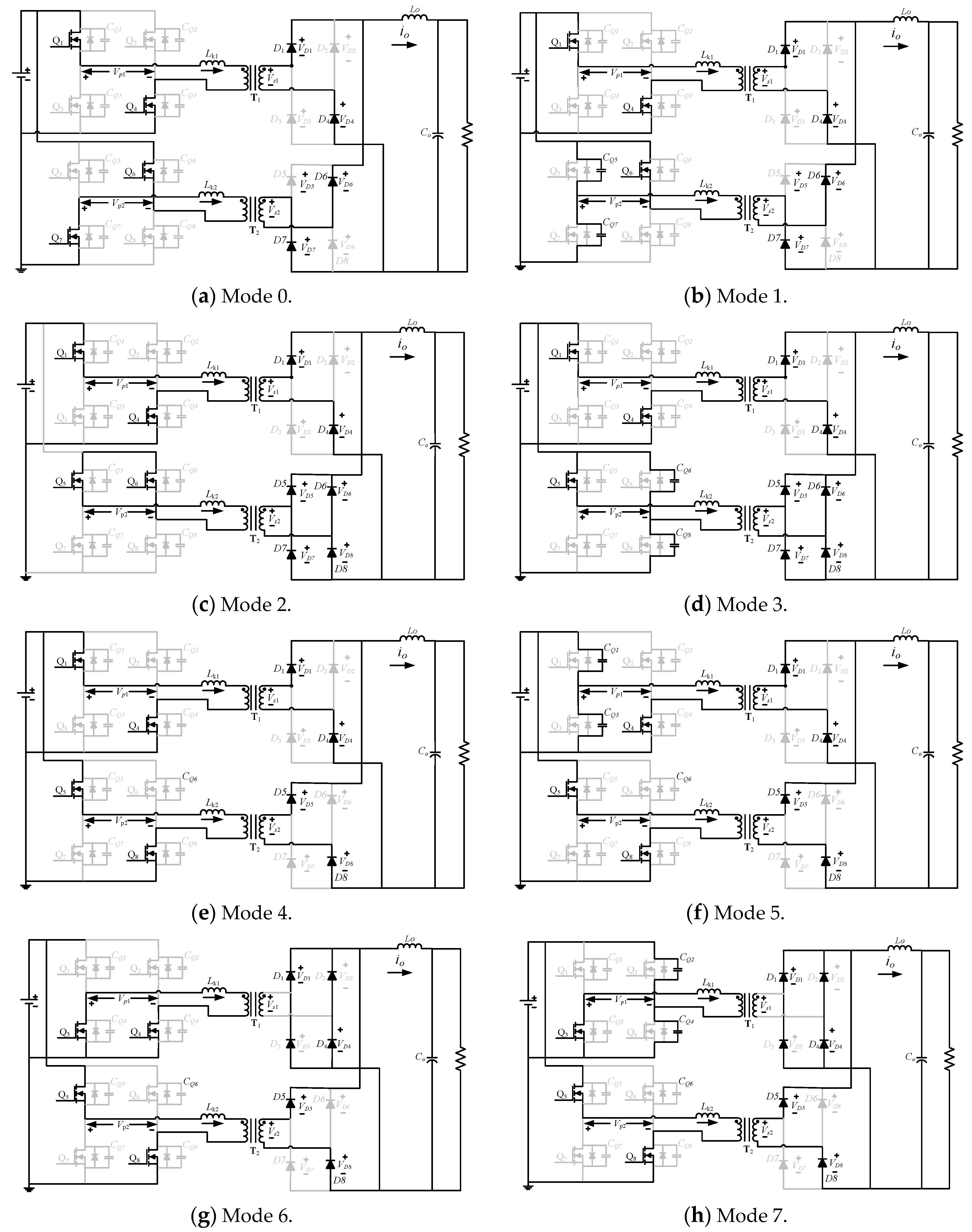
2. System Description

The switching control method of the PSFB is an extension of the traditional switching control method of the full-bridge converter. The circuit diagram of the proposed interleaved PSFB converter is shown in Figure 2. Phase 1 PSFB consists of four metal–oxide–semiconductor field-effect transistors (MOSFETs) Q1–Q4, Transformer T1, a series inductor Lk1, a secondary rectifier with four diodes D1–D4, and an output choke Lo. Phase 2 PSFB consists of four MOSFETs Q5–Q8, Transformer T2, a series inductor Lk2, and a secondary rectifier with four diodes D5–D8. The operation of the proposed PSFB, which is a combination of two phases, can be generally divided into different operation modes. The key waveforms of the proposed converter are shown in Figure 3, and the assumptions on which they are based are presented as follows.
(1)
The magnetizing inductance Lm and the output inductors Lo are large enough to be considered as a constant current source during the dead time of the primary switches.
(2)
Resonances by parasitic components are ignored, except for Phase 1 resonance between Lk1 and the parasitic capacitor of Q1–Q4 and Phase 2 resonance Lk2 and the parasitic capacitor of Q5–Q8.
(3)
The turns ratio of the coupled inductor is 1:1, and it has a high coupled coefficient.
The control method is pulse-width modulation with phase-shift, which has broader controllability and an easier design compared to the control method of frequency modulation. Therefore, the operating modes are symmetrical, and a half cycle is described in this paper. The half cycle can be divided into eight modes. The equivalent circuit is shown in Figure 4. The second half of the switching cycle is symmetrical with the above description.
Mode 0 (t0t1): In this mode, Q1, Q4, Q6, and Q7 are turned on. Energy is transferred to the secondary diodes through the transformer T1. The secondary diodes D1 and D4 conduct. In this interval, iLo increases at the slope of (nVinVo)/Lo. When Q7 turns off at t1, this mode ends.
Mode 1 (t1t2): Q7 ends at t1, and the circulating current charges CQ7 and discharges CQ5. The iLk2 current can be regarded as a constant current source in this interval. When the Q5 drain-to-source voltage reaches zero at t5, this mode ends.
Mode 2 (t2t3): During this time interval, current commutation is completed at t2. The secondary diodes D6 and D7 conduct. When Q6 turns off at t3, this mode ends.
Mode 3 (t3t4): Q6 ends at t3, and the circulating current charges CQ6 and discharges CQ8. The iLk2 current can be regarded as a constant current source in this interval. When the Q8 drain-to-source voltage reaches zero at t4, this mode ends.
Mode 4 (t4t5): In this interval, the Q8 drain-to-source voltage reaches zero, contributed by the iLk2 current. Q8 is turned on, and the secondary diodes D5 and D8 conduct. When Q1 turns off at t5, this mode ends.
Modes 5–7 (t5t8): This interval is similar to (t1t4) due to the circuit symmetry. The master phase circulates on the primary side, and the other phase transfers energy to the load.
In the proposed PSFB, the dual-loop control scheme is employed, and the control circuit is implemented using error amplifiers. It can provide the required phase margin and low-frequency gain to achieve stability with higher bandwidth. Figure 5 illustrates that a voltage divider, a current detection resistor Rshunt, amplifiers, and compensated network consist of a feedback controller. The output of the voltage loop error amplifier provides the current reference for the current loop error amplifier, which is used to realize the current control and current sharing of the two phases and generate the PWM signal with the phase-shift angles between the bridge legs.

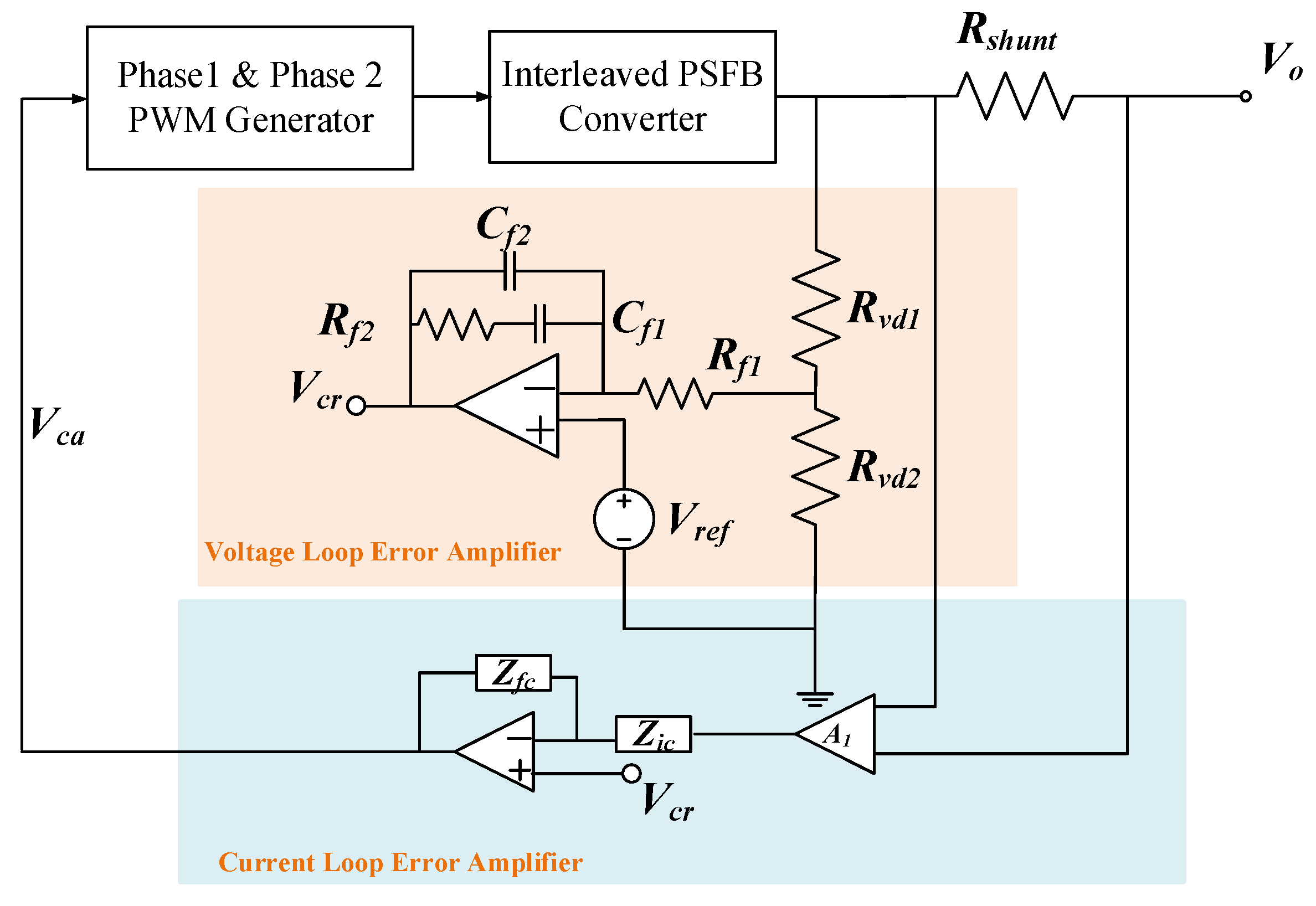
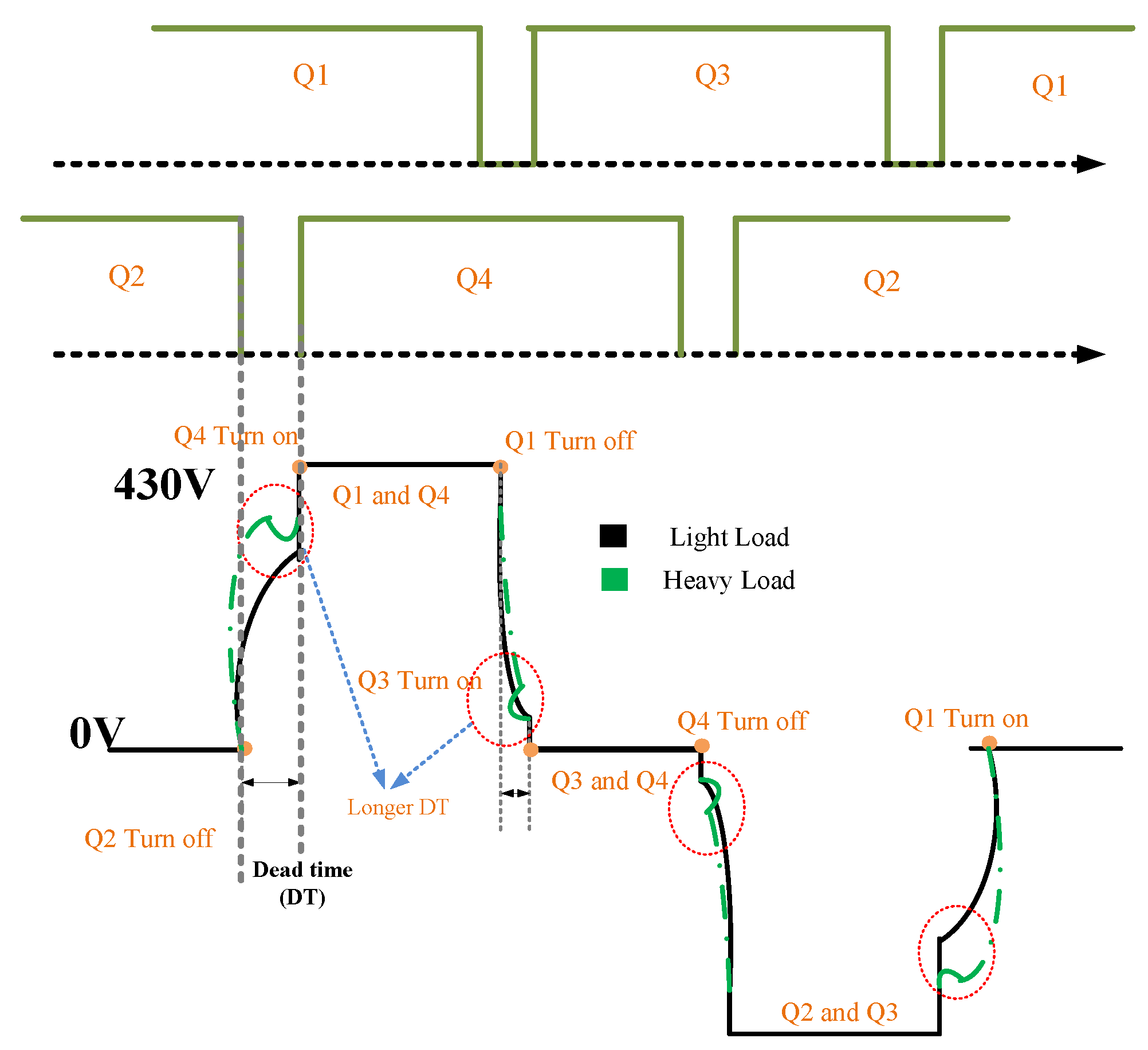
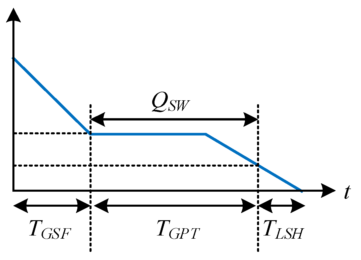
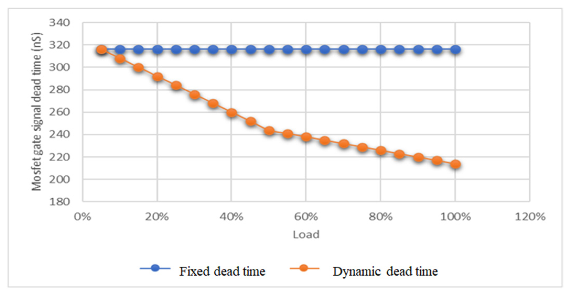
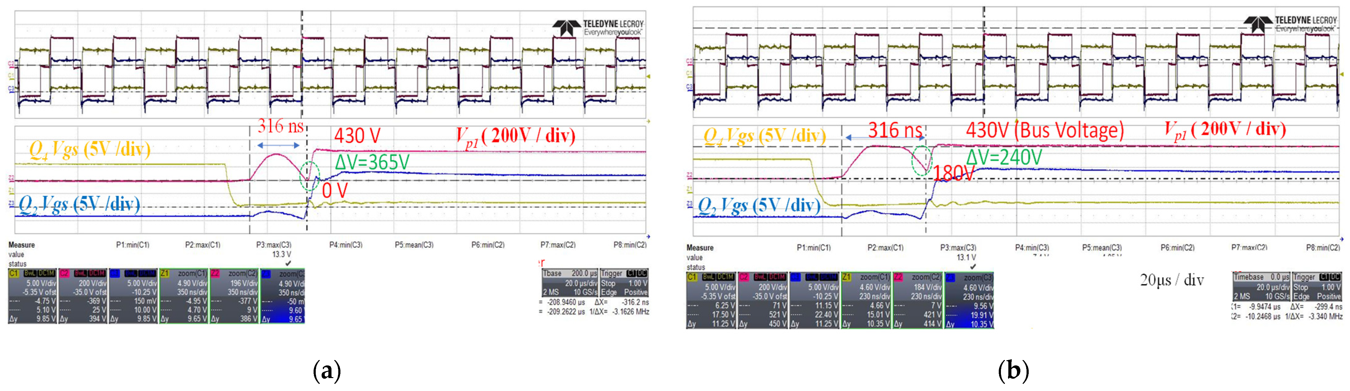
3. Dynamic Dead Time Control

In this paper, dynamic dead time control is proposed for different output loads. In general, it is always desirable to provide an optimally minimized dead time without running into shoot-through conditions. However, achieving ZVS at light loads with a minimized dead time is challenging. Under no-load and light load conditions, ZVS may be lost if the inductive energy available in the circuit is insufficient to charge and discharge the output capacitance of the two MOSFETs in the same bridge leg. Therefore, for no/light load, a longer dead time is usually preferred, but the longer dead time leads to longer body diode conduction and a consequent loss of efficiency. Moreover, the expense of dead time will result in lower conversion efficiency, and the ZVS advantages cannot be the perfect present under heavy loads. Figure 6 shows the transformer waveform with a fixed dead time. It can be found that a voltage drop occurs with a longer fixed dead time. Even though ZVS may be achieved under the light load condition, the overall conversion efficiency could be lower. Figure 7 illustrates the transformer waveform with dynamic dead time control.
The controller can be optimized during the dead time between the low-side and high-side MOSFET depending on the load condition. ZVS can be achieved under heavy load conditions, and the switching loss can be reduced under light load conditions. Consequently, the output current can also be sensed from a current transformer, which is used for estimating the load conditions. Next, the optimal dead time can be determined.
Designing better dead time requires a detailed understanding of the transition process with different intervals. In practice, the transitions from a high level to a low level and a low level to a high level are not symmetrical. Additionally, the propagation delay through the driver stage may be added with IC-based gate drivers. To illustrate this analysis, the basic gate discharge waveform is used with a soft-switching full-bridge circuit. Figure 8 displays three distinct stages for gate discharge. Therefore, the minimum dead time requirement can be obtained as follows:
T D T T G S F + T G P T + T L S H + T D S D
where TGSF is the fall time in the first interval, TGPT is the sum of the voltage fall time and the current rise time during the period closed according to driving conditions, TLSH is the fall time in the last interval, and TDSD is the requirement of the output capacitor discharge time. The first and last time intervals in the basic gate discharge waveform can be approximated as follows:
T G S F = C G S × V G S V G I G o f f
T L S H = C G S × V T H I G o f f
where CGS is the equivalent gate-to-source capacitance, VGS is the high level of the gate voltage, VG is the Miller voltage, VTH is the threshold voltage of a MOSFET, and IGoff is the sink current of the driver. TGPT can be approximated:
T G P T = R G o f f × Q s w V G
where RGoff is the equivalent turn-off resistance, and QSW is the total switching charge. The output capacitor discharge time is required for a quarter of the resonant period of the equivalent PCB trace inductance and output capacitor. TDSD can be derived as follows:
T D S D = π 2 × L P C B × Q o s s V i n
where LPCB is the equivalent PCB trace inductance, and QOSS is the output capacitor charge. The aforementioned approach is a simple means by which to design the dead time. However, the results may not be reliable because of the uncertain output capacitance and equivalent inductance under different load conditions. To approximate the output capacitor discharge time with the output current, (5) can be further modified as follows:
T D S D = π 2 × 2 L m C o s s i C T
where Lm is the magnetizing inductance, COSS is the output capacitance of the MOSFET, n is the turn ratio, and iCT is the primary peak current, which is related to the output current. In addition, the capacitance across the MOSFET could be changed with the applied voltage across the transistor. The total equivalent capacitance across the transistor could be influenced by the circuit layout. Hence, it is necessary to calibrate the calculation and determine the effective capacitance after the hardware circuit is implemented.
In this paper, two interleaved PSFB converters are made to operate in an interleaving fashion. By shifting the duty cycles of adjacent channels at 90°, the output current ripple can be reduced. Moreover, the second converter is closed when the load condition is under 20% rated load. As the output current increases under light load conditions, the switching loss is reduced because of ZVS, thus yielding higher conversion efficiency.

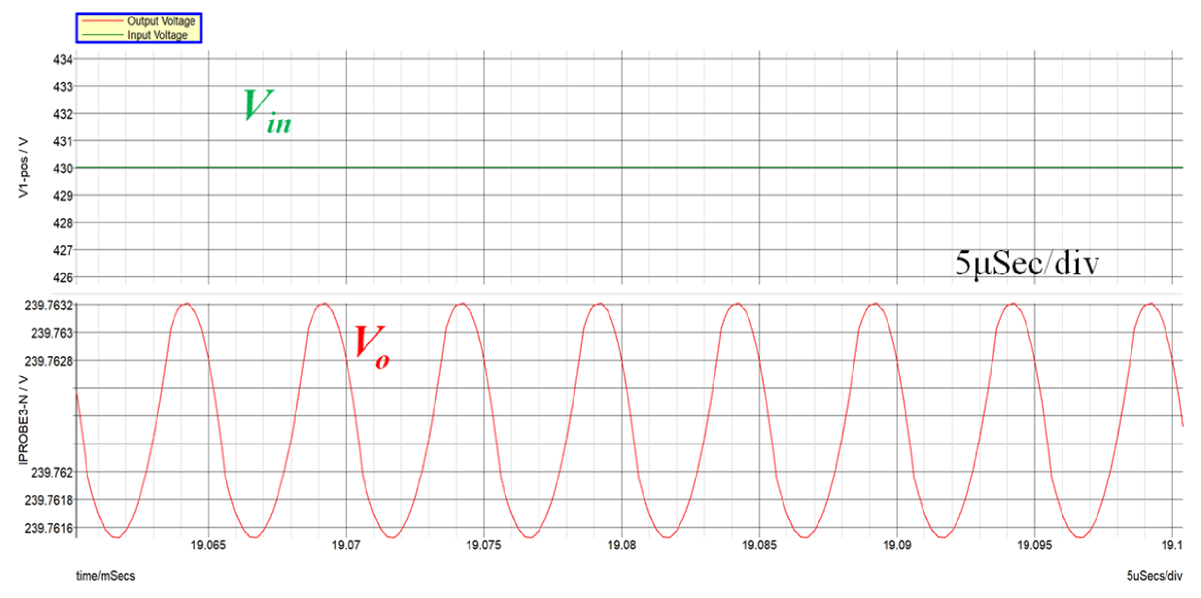
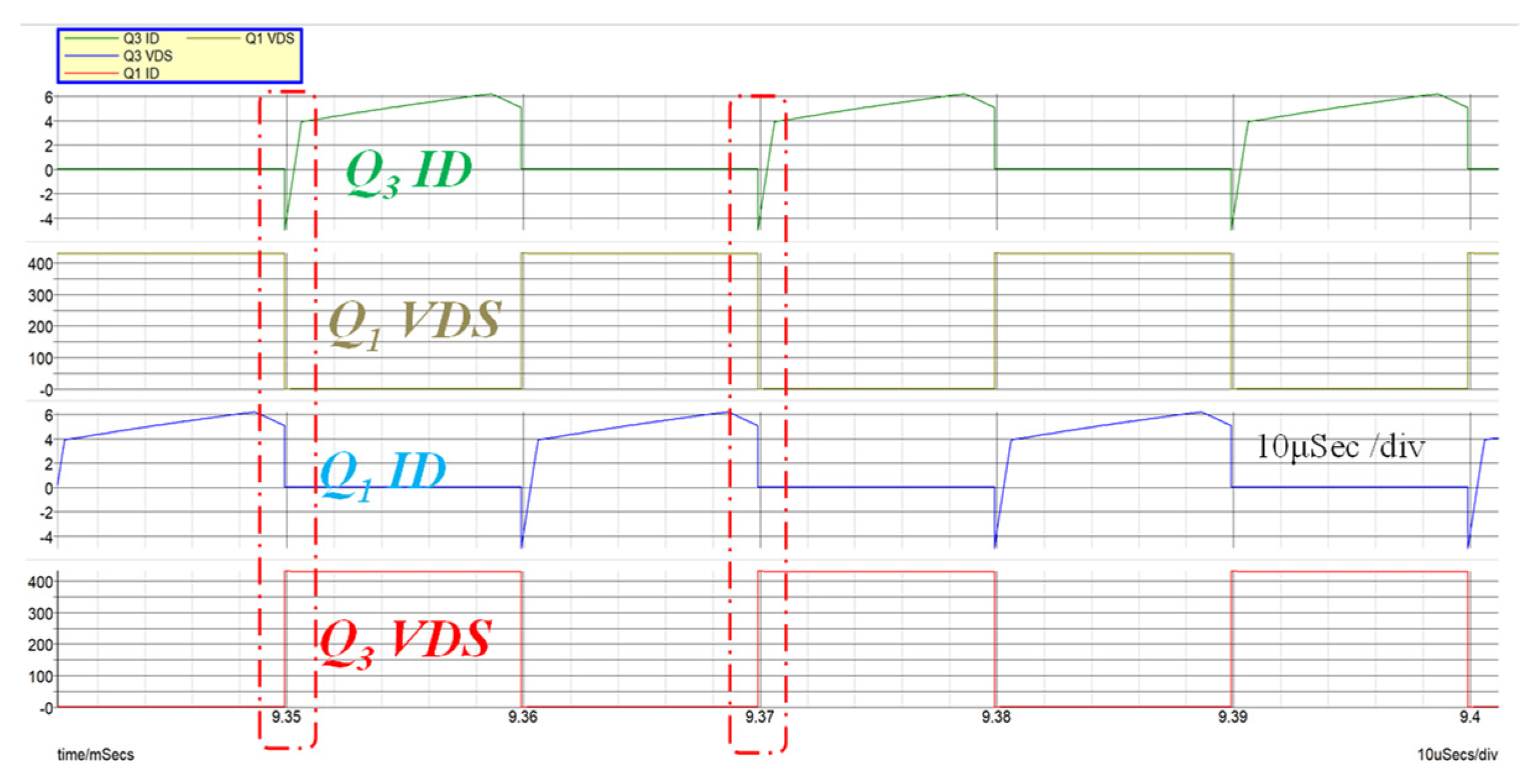
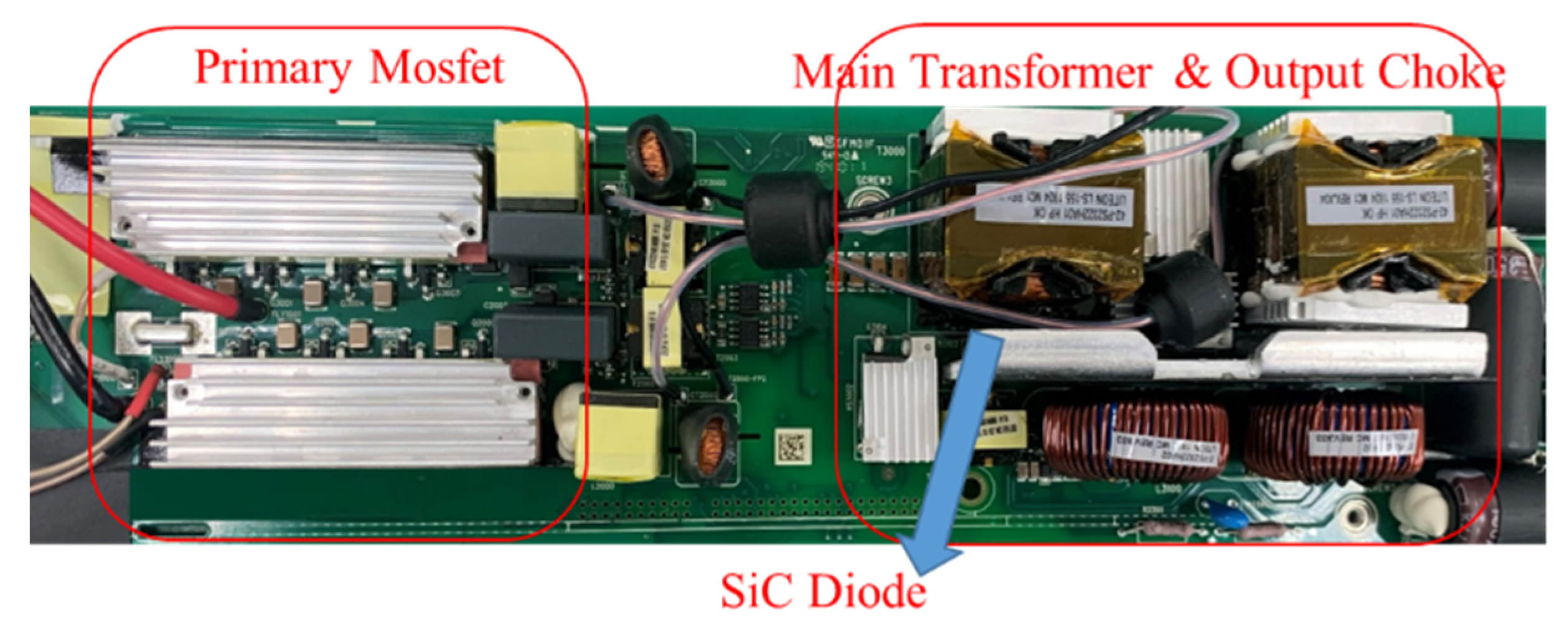
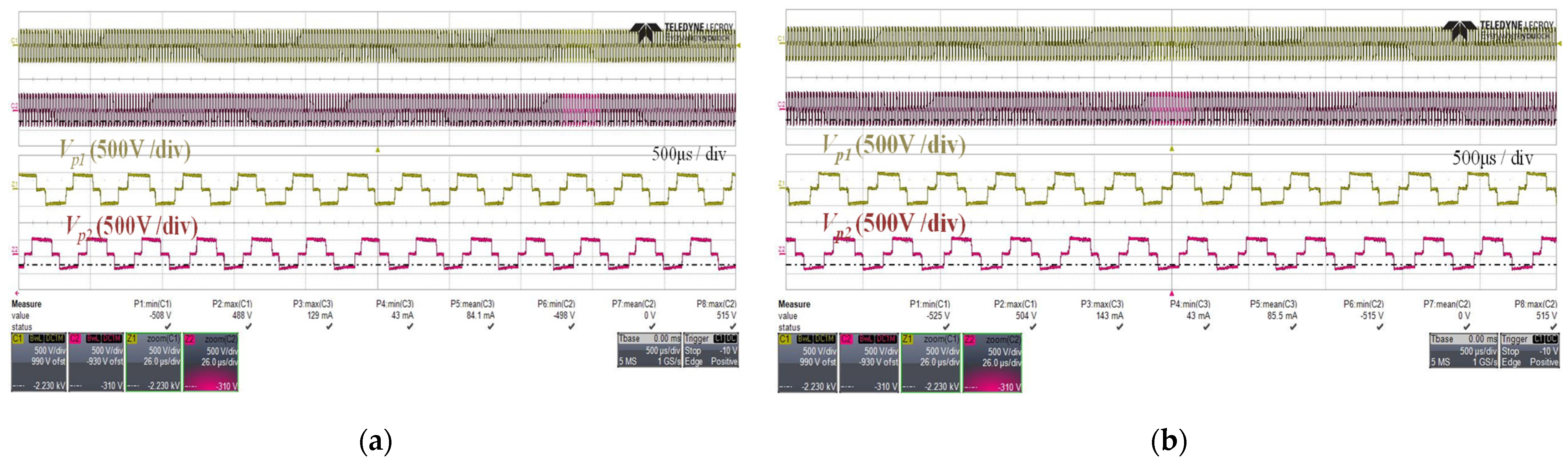
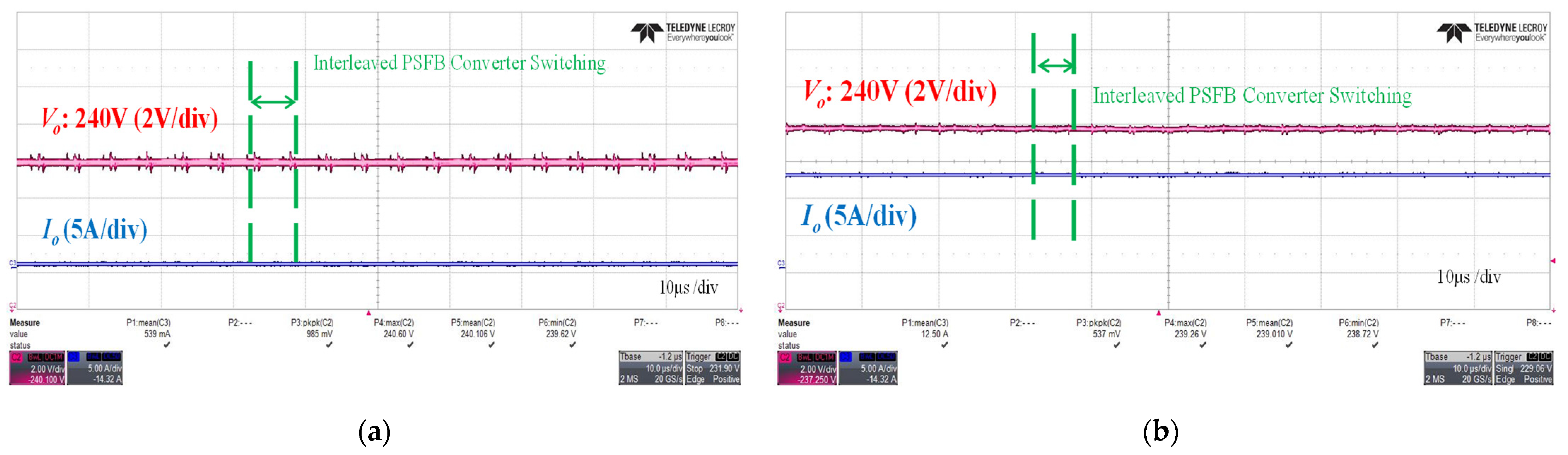
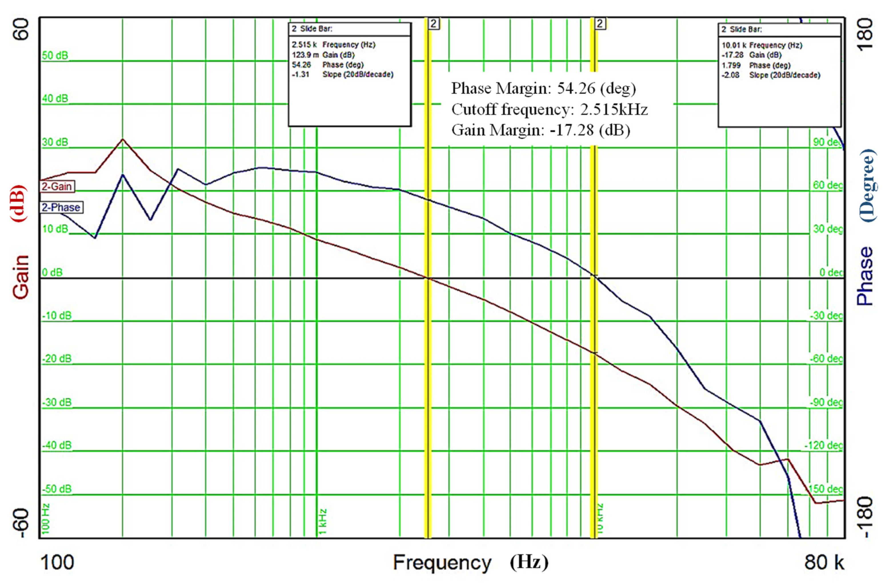
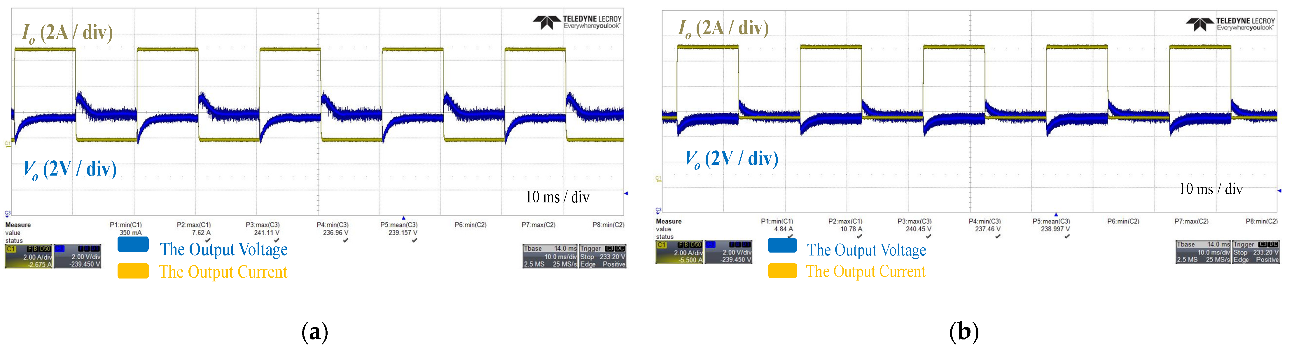
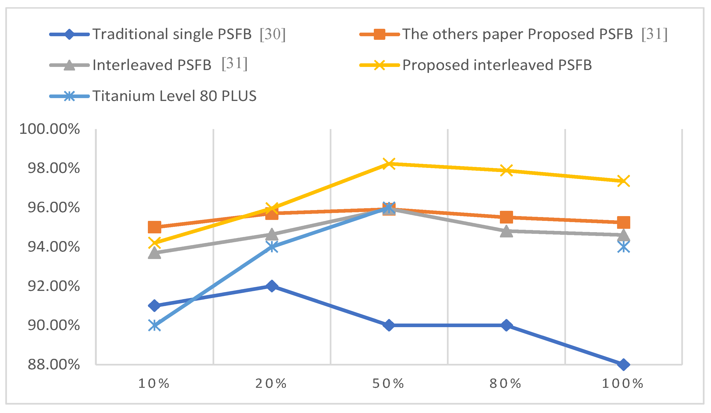
4. Computer Simulations and Experimental Results

A 430 V to 240 V 3 kW interleaved PSFB converter with dynamic dead time control was designed for validation. Table 1 lists the key parameters of the proposed converter prototype. From 1 to 5, the dynamic dead time and traditional dead time can be obtained, as shown in Figure 9.
The computer simulations shown in Figure 10 are the input and output voltage waveforms of the proposed PSFB converter with dynamic dead time control. It is obvious that the output voltage ripple is reduced significantly. The voltages across the phase-shifted primary and secondary high-frequency transformers are shown in Figure 11 and Figure 12, respectively. Another key feature of the PSFB converter is the ZVS. Figure 13 shows the simulated drain current and drain-to-source voltage waveforms of the two MOSFETs in the same bridge leg. ZVS is achieved under the rated power in the simulations.
The parameters in Table 1 are adopted, and a 430 V to 240 V 3 kW interleaved PSFB converter with dynamic dead time control was designed for validation. Figure 14 shows a photograph of the experimental prototype. The experimental waveforms of the proposed converter are shown in Figure 15 and Figure 16. Figure 15 illustrates the main waveforms of the midpoint voltage of the two bridges under two operating conditions, which is consistent with the theoretical analysis. Figure 16 shows the experimental waveforms of the output voltage and output current at no load and 3-kW-rated power. The output voltage is less than 1 V. It can be found that the output inductor ripple currents can cancel each other, and the output current ripple of the output capacitor can be reduced. Therefore, a small-sized inductor is possible, thus reducing the output filter weight.
For server power applications, the proposed PSFB converter is designed to be optimized for the highest efficiency at 50% load and the best thermal performance at 100% load. In order to verify the dynamic dead time control design, Figure 17 and Figure 18 are presented. Figure 17a shows the experimental waveforms with a fixed dead time at half of the rated load condition. Because the ZVS conditions of the heavy load are easier than those of light loads, we usually design a longer dead time for no light loads. Figure 17b illustrates the transformer waveforms with a fixed dead time under full load conditions. It can be observed that voltage drops of 365 V and 240 V occur at half of the rated load and full load when the Q2 switch is turned on. Figure 18 illustrates the corresponding waveforms with dynamic dead time under different load conditions. It can be observed that voltage drops of 90 V and 60 V occur at half of the rated load and full load when the Q2 switch is turned on. Compared with the fixed dead time control, the proposed dynamic dead time control makes an improvement of the voltage stress when the related switch is turned on. Figure 19 illustrates the experimental drain current and drain-to-source voltage waveforms of the Q1 switch. The ZVS can be achieved under rated power in the experiments.
Figure 20 illustrates the measured frequency response of the proposed PSFB converter with a voltage feedback controller in closed-loop operation. The bandwidth is observed as 2.5 kHz, and the voltage controller achieves a phase margin of 54° for stability. In practice, there is no significant difference for the stability margin between the fixed dead time control and dynamic dead time control. The prototype system may be implemented in a stable operation and equipped with low-frequency gain to improve the response speed. Figure 21a illustrates the experimental transient waveforms when the dynamic load is performed from no load to 60% load. Figure 21b illustrates the experimental transient waveforms when the dynamic load is performed from 40% load to full load. Under both conditions, the output voltage ripple is reduced significantly. The power conversion efficiency of the proposed PSFB converter under different output power is demonstrated in Figure 22, which shows the peak efficiency of approximately 98%. In addition, the efficiency curve is compared with other PSFB converters. Reference [30] used a typical PSFB converter configuration with a modified synchronized rectifier to achieve a higher conversion efficiency. Reference [31] presented an interleaved PSFB with new coupled inductor rectifiers to reduce the primary circulating current. Compared to other works, the proposed converter has higher conversion efficiency that can achieve the 80 Plus Titanium level.

5. Conclusions

An optimized dead time for the PSFB converter is proposed in this paper. Based on the proposed dead time control, the switching characteristics and half load conditions are analyzed in detail. Further, the dead time is recommended to provide a natural burst mode operation, which results in low power consumption and excellent thermal performance under both heavy and extreme loads. All these improvements have been validated experimentally by using a 3 kW prototype. The experimental results confirmed that the conversion efficiency is as high as 97.2% at the rated power of 3 kW and 92.95% at the light load of 300 W. The experimental transient waveforms demonstrated that the voltage spike or drop is less than 2 V in the fast-fluctuating load conditions from 0% load to 60% load and 40% load to 100% load.

Author Contributions

All authors have contributed significantly to this research in all stages of the study. Conceptualization, J.-Y.L.; methodology, J.-Y.L., K.-Y.L., and J.-H.C.; formal analysis, J.-Y.L., K.-Y.L., and J.-H.C.; computer software simulation, J.-H.C.; system hardware implementation, J.-H.C.; writing, K.-Y.L. and J.-H.C.; review and editing, J.-Y.L., K.-Y.L., and J.-H.C. All authors have read and agreed to the published version of the manuscript.

Funding

This research was funded by the Ministry of Science and Technology, Taiwan, grant number MOST-109-2221-E-006-082.

Conflicts of Interest

The authors declare no conflict of interest.

References

  1. Yadav, G.N.B.; Narasammaand, N.L. An active soft switched phaseshifted full-bridge DC–DC converter: Analysis, modeling, design, and implementation. IEEE Trans. Power Electron. 2014, 29, 4538–4550. [Google Scholar] [CrossRef]
  2. Cho, J.H.; Seong, H.W.; Jung, S.M.; Park, J.S.; Moon, G.W.; Youn, M.J. Implementation of digitally controlled phase shift full bridge converter for server power supply. In Proceedings of the 2010 IEEE Energy Conversion Congress and Exposition, Atlanta, GA, USA, 12–16 September 2010; pp. 802–809. [Google Scholar]
  3. Cho, S.Y.; Kim, J.K.; Lee, I.W.; Kim, M.Y.; Moon, G.W. High efficiency standby forward converter integrated with DC/DC phase-shift full bridge converter for server power supply system. In Proceedings of the 8th International Conference on Power Electronics—ECCE Asia, Jeju, Korea, 30 May–3 June 2011; pp. 1169–1176. [Google Scholar]
  4. Lee, S.-H.; Park, C.-Y.; Kwon, J.-M.; Kwon, B.-H. Hybrid-Type fullbridge DC/DC converter with high efficiency. IEEE Trans. Power Electron. 2015, 30, 4156–4164. [Google Scholar] [CrossRef]
  5. Wu, H.; Zhang, J.; Qin, X.; Mu, T.; Xing, Y. Secondary-Side-Regulated soft-switching full-bridge three-port converter based on bridgeless boost rectifier and bidirectional converter for multiple energy interface. IEEE Trans. Power Electron. 2016, 31, 4847–4860. [Google Scholar] [CrossRef]
  6. Li, H.; Zhao, L.; Xu, C.; Zheng, X. A dual half-bridge phase-shifted converter with wide ZVZCS switching range. IEEE Trans. Power Electron. 2018, 33, 2976–2985. [Google Scholar] [CrossRef]
  7. Kanamarlapudi, V.R.K.; Wang, B.; So, P.L.; Wang, Z. Analysis, design, and implementation of an APWM ZVZCS full-bridge DC–DC converter for battery charging in electric vehicles. IEEE Trans. Power Electron. 2017, 32, 6145–6160. [Google Scholar] [CrossRef]
  8. Kim, Y.-D.; Lee, I.-O.; Cho, I.-H.; Moon, G.-W. Hybrid dual fullbridge DC–DC converter with reduced circulating current, output filter, and conduction loss of rectifier stage for RF power generator application. IEEE Trans. Power Electron. 2014, 29, 1069–1081. [Google Scholar]
  9. Shih, L.-C.; Liu, Y.-H.; Chiu, H.-J. A novel hybrid mode control for phase-shift full bridge converter featuring high efficiency over full load range. IEEE Trans. Power Electron. 2019, 34, 2794–2804. [Google Scholar] [CrossRef]
  10. Kim, D.-Y.; Kim, C.-E.; Moon, G.-W. Variable dead time method in the phase-shifted full-bridge converter for reduced power consumption under light load conditions. IEEE Trans. Power Electron. 2013, 28, 5120–5127. [Google Scholar] [CrossRef]
  11. Kim, J.-W.; Kim, D.-Y.; Kim, C.-E.; Moon, G.-W. A simple switching control technique for improving light load efficiency in a phase-shifted full-bridge converter with a server power system. IEEE Trans. Power Electron. 2014, 29, 1562–1566. [Google Scholar] [CrossRef]
  12. Joo, D.M.; Lee, B.K.; Kim, J.S. Dead-time optimisation for a phaseshifted DC–DC full bridge converter with GaN HEMT. IET Electron. Lett. 2016, 52, 769–770. [Google Scholar] [CrossRef]
  13. Yu, W.; Lai, J.-S.; Lai, W.-H.; Wan, H. Hybrid resonant and PWM converter with high efficiency and full soft-switching range. IEEE Trans. Power Electron. 2012, 27, 4925–4933. [Google Scholar] [CrossRef]
  14. Lee, I.-O.; Moon, G.-W. Soft-Switching DC/DC converter with a full ZVS range and reduced output filter for high-voltage applications. IEEE Trans. Power Electron. 2013, 28, 112–122. [Google Scholar] [CrossRef]
  15. Lee, I.-O.; Moon, G.-W. Phase-shifted PWM converter with a wide ZVS range and reduced circulating current. IEEE Trans. Power Electron. 2013, 28, 908–919. [Google Scholar] [CrossRef]
  16. Safaee, A.; Jain, P.; Bakhshai, A. A ZVS pulsewidth modulation fullbridge converter with a low-RMS-current resonant auxiliary circuit. IEEE Trans. Power Electron. 2016, 31, 4031–4047. [Google Scholar] [CrossRef]
  17. Zhao, L.; Li, H.; Wu, X.; Zhang, J. An improved phase-shifted fullbridge converter with wide-range ZVS and reduced filter requirement. IEEE Trans. Ind. Electron. 2018, 65, 2167–2176. [Google Scholar] [CrossRef]
  18. Park, K.-B.; Kim, C.-E.; Moon, G.-W.; Youn, M.-J. Voltage oscillation reduction technique for phase-shift full-bridge converter. IEEE Trans. Ind. Electron. 2007, 54, 2779–2790. [Google Scholar] [CrossRef]
  19. Miftakhutdinov, R. New aspects on analyzing ZVS conditions for converters using super-junction Si and wide bandgap SiC and GaN power FETs. In Proceedings of the 2014 16th European Conference on Power Electronics and Applications, Lappeenranta, Finland, 26–28 August 2014; pp. 1–9. [Google Scholar]
  20. Kasper, M.; Burkart, R.M.; Deboy, G.; Kolar, J.N. ZVS of power MOSFETs revisited. IEEE Trans. Power Electron. 2016, 31, 8063–8067. [Google Scholar] [CrossRef]
  21. Tran, D.D.; Vu, H.N.; Yu, S.; Choi, W. A Novel soft-switching full-bridge converter with a combination of a secondary switch and a nondissipative snubber. IEEE Trans. Power Electron. 2018, 33, 1440–1452. [Google Scholar] [CrossRef]
  22. Kishore, K.V.R.; Wang, B.F.; Kumar, K.N.; So, P.L. A new ZVS full-bridge DC-DC converter for battery charging with reduced losses over full-load range. IEEE Trans. Ind. Appl. 2018, 54, 571–579. [Google Scholar]
  23. Shen, Y.; Zhao, W.; Chen, Z.; Cai, C. Full-bridge LLC resonant converter with series-parallel connected transformers for electric vehicle onboard charger. IEEE Access. 2018, 6, 13490–13500. [Google Scholar] [CrossRef]
  24. Gu, B.; Lai, J.-S.; Kees, N.; Zheng, C. Hybrid-switching fullbridge dc-dc converter with minimal voltage stress of bridge rectifier, reduced circulating losses, and filter requirement for electric vehicle battery chargers. IEEE Trans. Power Electron. 2013, 28, 1132–1144. [Google Scholar] [CrossRef]
  25. Redl, R.; Sokal, N.O.; Balogh, L. A novel soft-switching full-bridge DC/DC converter: Analysis design considerations and experimental results at 1.5 kW, 100 kHz. IEEE Trans. Power Electron. 1991, 6, 408–418. [Google Scholar] [CrossRef]
  26. Kim, E.-S.; Kim, Y.-H. A ZVZCS PWM FB DC/DC converter using a modified energy-recovery snubber. IEEE Trans. Ind. Electron. 2002, 49, 1120–1127. [Google Scholar]
  27. ST Microelectronics AN5018. Calculation of Turn-Off Power Losses Generated by an Ultrafast Diode; STMicroelectronics: Geneva, Switzerland, 2017; pp. 1–20. Available online: https://www.st.com/resource/en/application_note/dm00380483-calculation-of-turnoff-power-losses-generated-by-a-ultrafast-diode-stmicroelectronics.pdf (accessed on 1 January 2021).
  28. Baliga, B.J. Fundamentals of Power Semiconductor Devices; Springer: New York, NY, USA, 2008. [Google Scholar]
  29. Erickson, R.W.; Maksimovic, D. Fundamentals of Power Electronics, 2nd ed.; Kluwer: Norwell, MA, USA, 2001. [Google Scholar]
  30. Ogale, A.; Sarlioglu, B.; Wang, Y. A Novel Design and Performance Characterization of a Very High Current Low Voltage DC-DC Converter for Application in Micro and Mild Hybrid Vehicles. In Proceedings of the IEEE Applied Power Electronics Conference and Exposition, Charlotte, NC, USA, 15–19 March 2015. [Google Scholar]
  31. Han, J.K.; Moon, G.W. High-Efficiency Phase-Shifted Full-Bridge Converter with a New Coupled Inductor Rectifier (CIR). IEEE Trans. Power Electron. 2019, 34, 8468–8480. [Google Scholar] [CrossRef]
  32. Zhang, M.T.; Jovanovic, M.M.; Lee, F.C. Analysis and evaluation of interleaving techniques in forward converters. IEEE Trans. Power Electron. 1998, 13, 690–698. [Google Scholar] [CrossRef] [Green Version]
  33. Wu, X.; Chen, H.; Zhang, J.; Peng, F.; Qian, Z. Interleaved phase-shift full-bridge converter with transformer winding series-parallel autoregulated (SPAR) current doubler rectifier. IEEE Trans. Power Electron. 2015, 30, 4864–4873. [Google Scholar] [CrossRef]
Figure 1. Major topics of development technology in recent years.
Energies 14 00853 g001
Figure 2. Circuit diagram of the proposed phase-shift full-bridge (PSFB) converter.
Energies 14 00853 g002
Figure 3. Key waveforms of the proposed PSFB converter.
Energies 14 00853 g003
Figure 4. Operation modes of the proposed PSFB.
Energies 14 00853 g004
Figure 5. Dual-loop controller of the proposed PSFB.
Energies 14 00853 g005
Figure 6. Theoretical transformer waveform with a fixed dead time.
Energies 14 00853 g006
Figure 7. Theoretical transformer waveform with dynamic dead time control.
Energies 14 00853 g007
Figure 8. Gate turn-off voltage and time intervals.
Energies 14 00853 g008
Figure 9. Fixed dead time and dynamic dead time as functions of load.
Energies 14 00853 g009
Figure 10. Simulated waveforms of the input voltage and output voltage.
Energies 14 00853 g010
Figure 11. Simulated waveforms of the primary voltage across the transformers.
Energies 14 00853 g011
Figure 12. Simulated waveform of the secondary voltage across the transformers.
Energies 14 00853 g012
Figure 13. Simulated waveforms of the drain current and drain-to-source voltage across the MOSFETs in the same bridge leg.
Energies 14 00853 g013
Figure 14. Prototype photograph.
Energies 14 00853 g014
Figure 15. Experimental waveforms of the primary voltage across the transformers. (a) At half-rated load. (b) At 3-kW-rated load.
Energies 14 00853 g015
Figure 16. Experimental waveforms of the output voltage and output current. (a) At no load. (b) At 3-kW-rated load.
Energies 14 00853 g016
Figure 17. Experimental transformer waveform with a fixed dead time. (a) At half-rated load. (b) At full load.
Energies 14 00853 g017
Figure 18. Experimental transformer waveform with dynamic dead time. (a) At half-rated load. (b) At full load.
Energies 14 00853 g018
Figure 19. Zero-voltage switching (ZVS) waveforms of Q1 at a 12.5A load.
Energies 14 00853 g019
Figure 20. Frequency response of the PSFB converter.
Energies 14 00853 g020
Figure 21. Experimental transient waveforms when the dynamic load is performed. (a) From no load to 60% load. (b) From 40% load to full load.
Energies 14 00853 g021
Figure 22. Measured conversion efficiency curves.
Energies 14 00853 g022
Table 1. Ratings and circuit parameters of the prototype PSFB converter.
Power rating3 kW
Input voltage, Vin390 VDC−450 VDC
Output voltage, Vout240 VDC ± 5V
Max. output current, Iomax12.5 A
Min. output current, Iomin0.05 A
Switching frequency, fs50 kHz
MOSFETsIPP60R120C7
Secondary Rectification DiodeSTPSC10H065DI
Transformer CorePQ3230
Transformer turns radioNp: Ns = 37:30
Magnetizing inductance, Lm2.6 mH
Output inductance392 μH
Blocking capacitor1 μF
Diver ICADUM4223ARWZ-RL
Publisher’s Note: MDPI stays neutral with regard to jurisdictional claims in published maps and institutional affiliations.

