Article

Modified Power Factor Correction (PFC) Control and Printed Circuit Board (PCB) Design for High-Efficiency and High-Power Density On-Board Charger

1
Department of Electrical Engineering, Princeton University, Princeton, NJ 08540, USA
2
School of Electrical Engineering, KAIST, Daejeon 34141, Korea
3
Department of Electrical Engineering, Incheon National University, 119, Academy-ro, Yeonsu-gu, Incheon 406840, Korea
*
Author to whom correspondence should be addressed.
Energies 2021, 14(3), 605; https://doi.org/10.3390/en14030605
Submission received: 24 December 2020 / Revised: 17 January 2021 / Accepted: 21 January 2021 / Published: 25 January 2021

Abstract

:
This paper presents a modified power factor correction (PFC) ON/OFF control and three-dimensional (3D) printed circuit board (PCB) design for a high-efficiency and high-power density onboard charger (OBC). By alternately operating one of two boost modules of the PFC stage at a 50% or less load condition, the proposed PFC control can reduce the load-independent power loss of the PFC stage, such as core loss and capacitor charging loss of switches. It enables OBCs to have high efficiency across a wide output power range and better thermal performance. The 3D-PCB design decouples a trade-off relationship of the PCB trace design and heat spreader design, increasing the power density of OBCs. A 3.3 kW prototype composed of an interleaved totem-pole bridgeless boost PFC converter and full-bridge (FB) LLC converter has been built and tested to verify the proposed PFC control and 3D-PCB effectiveness design. The prototype has 95.7% full power efficiency (98.2% PFC stage efficiency) and 52 W/in3 power density.

1. Introduction

Global warming issues, strict CO2 emission regulation, and high fuel economy demands are accelerating the transition from the automotive industry to electrified vehicles such as hybrid electric vehicles and electric vehicles [1,2,3]. In electrified vehicles, a high-voltage battery, i.e., the electric power source of the vehicle, is an essential part and is charged by off-board chargers or onboard chargers. The off-board charger, meaning the charger is exterior to the vehicle, achieves super-fast charging with over 50 kW high power capability. However, since particular infrastructure, such as a three-phase alternating current (AC) system and direct current (DC) system, is required for high power capability, the off-board charger is rarely able to be installed at the private consumer side. On the other hand, the onboard charger (OBC), meaning the charger is interior to the vehicle, has a slower charging time than the off-board charger due to lower power capability (e.g., 6.6 kW). Despite slow charging time, since the onboard charger enables private customers to charge vehicles at their home without high infrastructure cost, the OBC is also an essential part of electrified vehicles. In developing the OBC, high efficiency is essential to improve the fuel economy and reduce CO2 emissions. Moreover, high power density is also important, as the OBC is built into the engine and trunk rooms of electrified vehicles.
In general, the OBC consists of a power factor correction (PFC) stage and an isolated DC-DC stage to recharge the high-voltage battery from the AC grid [4,5,6,7,8,9]. Many topology and control studies have been conducted to improve the efficiency and power density of the OBC. For the PFC stage, boost-type topologies have been usually adopted [6,7,8,9]. Bridgeless boost-type topologies are preferred these days because they can eliminate large conduction loss of the bridge rectifier. Among bridgeless topologies, a totem-pole bridgeless boost PFC converter is becoming increasingly popular because of its simple structure, small conduction loss, low number of circuit elements, and low common mode noise problem [10,11,12,13,14,15,16]. Moreover, wide bandgap semiconductors, such as silicon-carbide (SiC) and gallium nitride (GaN), enable the totem-pole bridgeless converter to operate at high switching frequency in continuous current mode (CCM) operation. In applications above 3 kW, an interleaved structure is widely used to relieve a burden of semiconductor devices and input filter design [14,15,16]. The isolated DC-DC stage is typically implemented with soft switching topologies such as LLC converter, phase-shifted-full-bridge converter, and dual active bridge converter.
One of the important features of the OBC is that it should be able to cover a wide output power range because the charge capacity, i.e., maximum output power, of the OBC varies according to the input source such as dedicated electric vehicle supply equipment (EVSE) (e.g., dedicated charging station) and common household standard power outlet [17,18]. For instance, assuming that a 6.6 kW OBC is built in an electrified vehicle, the OBC can charge a battery with its maximum output power of 6.6 kW when the input source is dedicated EVSE. Here, the OBC should be designed to achieve high efficiency at 6.6 kW output. Meanwhile, when the input power comes from a household outlet, such as 220 VAC, the output power of the OBC should be degraded to 3.3 kW due to the power capacity limitation of the household outlet. Thus, the OBC should achieve high efficiency at both 3.3 kW and 6.6 kW output conditions. However, since semiconductor devices and passive components of the OBC are designed for achieving high efficiency at 6.6 kW output conditions, it is difficult to achieve high efficiency at 3.3 kW output conditions. This means that the OBC can achieve high efficiency with dedicated EVSE but has low efficiency at standard power outlet.
In this paper, a modified PFC ON/OFF control and effective printed circuit board (PCB) design method is presented to improve the efficiency and power density of OBCs comprising a PFC stage of the interleaved structure and a DC-DC stage. The modified PFC ON/OFF control enables the OBC to improve efficiency at 50% or less load condition. It makes only one of the interleaved PFC stage modules operate during a half line cycle of the AC input voltage. Namely, each phase of the interleaved PFC stage alternatively operates for every half-line cycle, which allows the PFC stage to have as high efficiency at half-load condition, as the full load efficiency is designed to be the highest efficiency. The thermal performance and lifetime of the OBC can also be improved with the proposed control. An effective three-dimensional (3D) PCB design method that uses top and bottom PCB design instead of a general single PCB design is also presented in this paper. Active and magnetic components that require a cooling system due to high power loss are placed on the bottom PCB with a heat spreader underneath. On the other hand, other components such as the large size of output capacitors and relay that do not need heat spreaders are put on the top PCB to reduce the board area. Consequently, this design method enables not only higher power density but also the optimal design of a cooling system that is related to fuel economy. The proposed methods can be applied to any interleaved PFC topologies and DC-DC topologies. In this paper, they are applied to a promising 3.3 kW OBC structure as an example, which comprises an interleaved totem-pole bridgeless boost PFC converter and LLC converter, to verify their effectiveness.

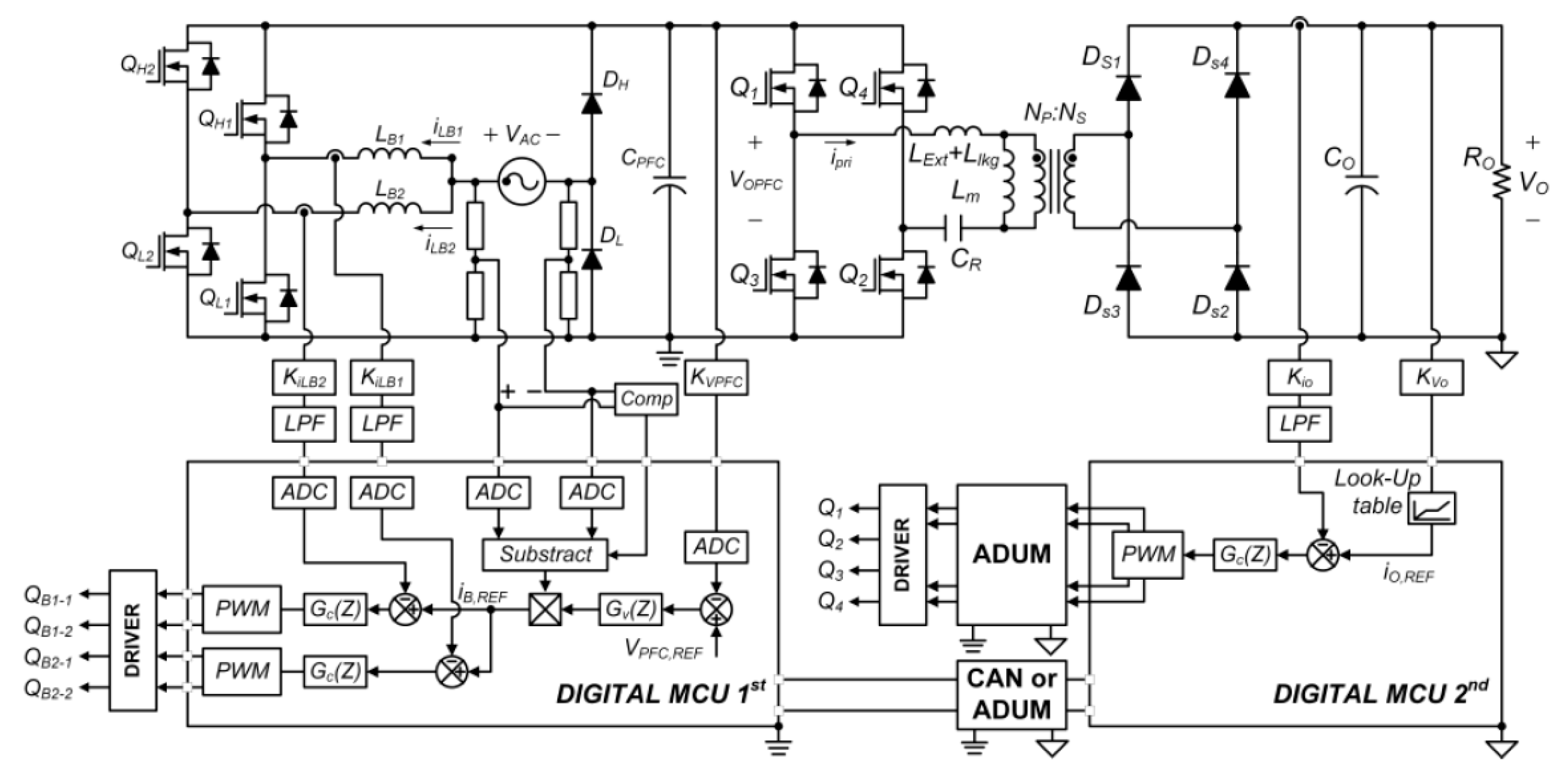
2. Modified PFC ON/OFF Control

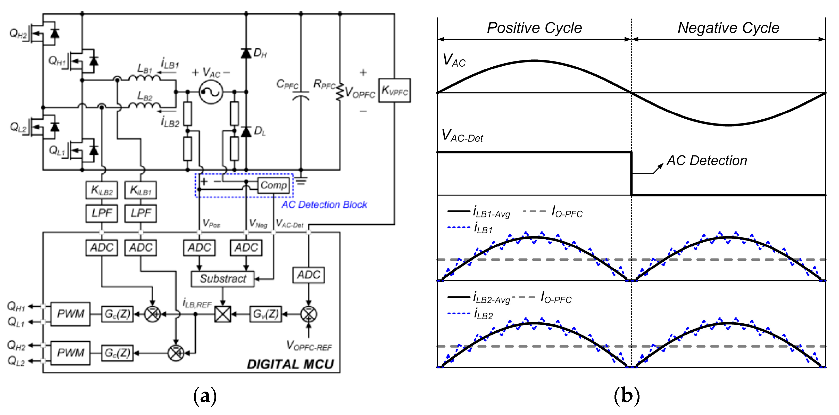
2.1. Conventional Interleaved Totem-Pole Bridgeless Boost PFC Converter

A circuit diagram of the conventional interleaved totem-pole bridgeless boost PFC converter with its control block diagram is shown in Figure 1. The interleaved totem-pole bridgeless boost converter is composed of two parallel connected boost modules. One boost module comprises a boost inductor (LB1) and two switches (QH1 and QL1), while subscript 2 indicates the second module. Since the role of the high side switch (QH) and low side switch (QL) is different according to positive and negative AC line cycles, the totem-pole bridgeless boost converter has to detect a direction of AC voltage (AC detection circuit), which is shown in Figure 1a. General control methods such as critical conduction mode (CRM) control and CCM control can be adopted according to the specifications of applications. In this paper, a CCM control with the average current control method, which regulates the average inductor current to follow the shape of AC input voltage, is used to reduce not only the conduction loss but also the burden of the electromagnetic interference (EMI) filter, as shown in Figure 1b. Each module is controlled to provide half of the total power during the AC line cycle (e.g., 50 Hz) and designed to achieve the highest efficiency at the full-load condition (PO-max), i.e., PO-max/2 for each module, by minimizing the conduction loss. In this design, the interleaved totem-pole bridgeless boost PFC converter can achieve its maximum efficiency at the full-load condition. However, at the half-load condition, each module transfers PO-max/4 and has a lower efficiency than the full load efficiency due to large load-independent loss such as core loss and capacitor charging loss of switches.

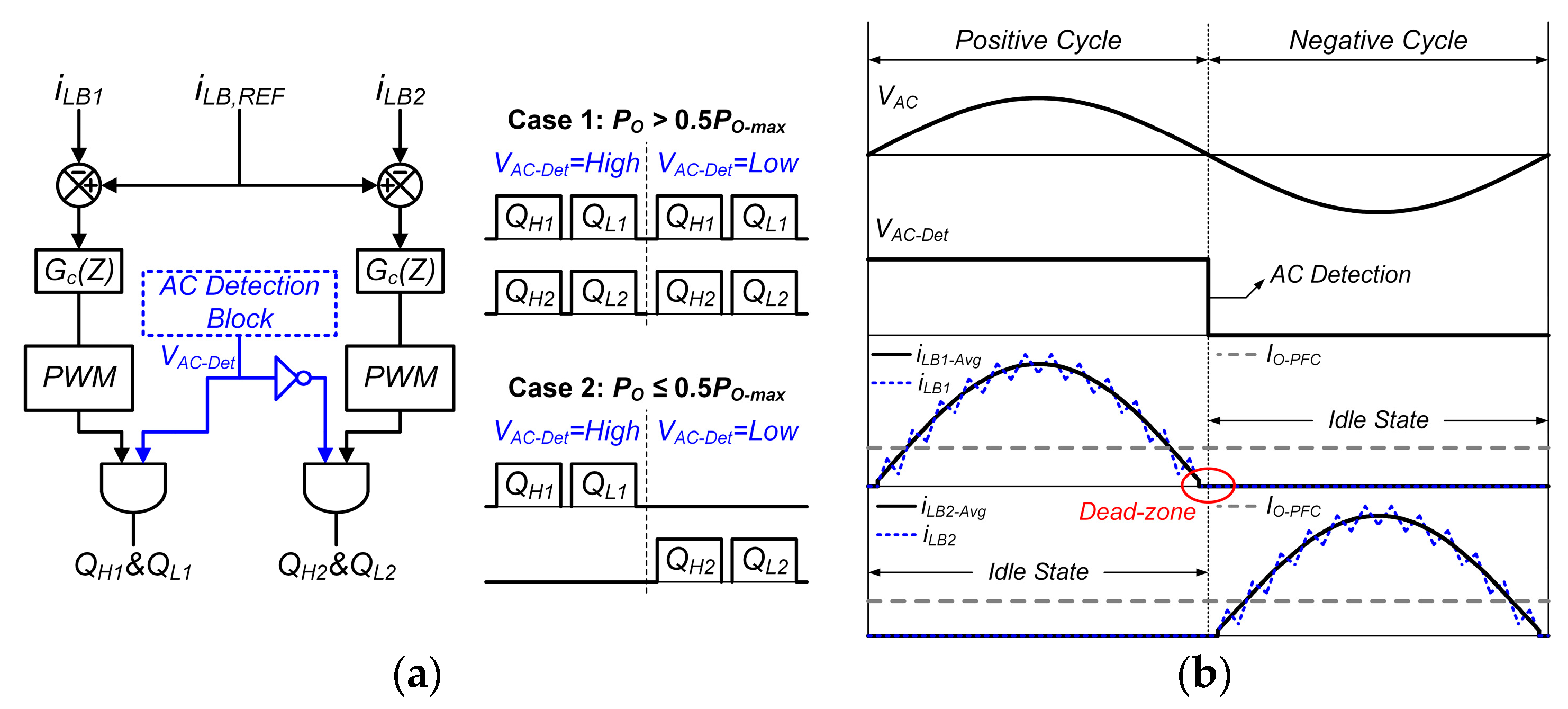
2.2. Concept of Modified PFC ON/OFF Control

This paper proposes a modified PFC ON/OFF control to maximize the OBC efficiency both at full and half-load conditions without any additional component. Figure 2 shows the key control block diagram and waveforms of the modified PFC ON/OFF control. As shown in Figure 2a, the modified ON/OFF control can be easily implemented using an already existing AC voltage detection circuit. When the output power is over PO-max/2, the modified ON/OFF control is inactive, and the PFC stage operates with the conventional interleaving control to maximize full load efficiency. While the ON/OFF control is activated at PO-max/2, it enables each module to operate alternately during the half AC line cycle to maximize half-load efficiency. Namely, as shown in Figure 2b, assuming half-load condition, each module delivers the average power of PO-max/2 during the active half cycle but zero during the other idle half cycle. Thus, each module delivers the average power of PO-max/4 during one AC line cycle such as the conventional control case. Since each module achieves the highest efficiency at PO-max/2, the modified PFC ON/OFF control allows the PFC stage to maximize half-load efficiency. Moreover, it can have the same maximum current stress as the conventional control, because the modified PFC ON/OFF control is only active at half or less load conditions. The modified PFC ON/OFF controller includes an enhanced duty ratio feed-forward technique [19] and dead-zone technique to minimize the zero-crossing current distortion and reset accumulated current control errors causing overshoots right after the zero-crossing. The current reference (iLB−REF) is set to be zero, and all switches are turned off during the dead-zone. Therefore, there is no inductor current near zero-crossing, and the modified PFC ON/OFF method enables each module to operate alternatively without any current distortion problem.

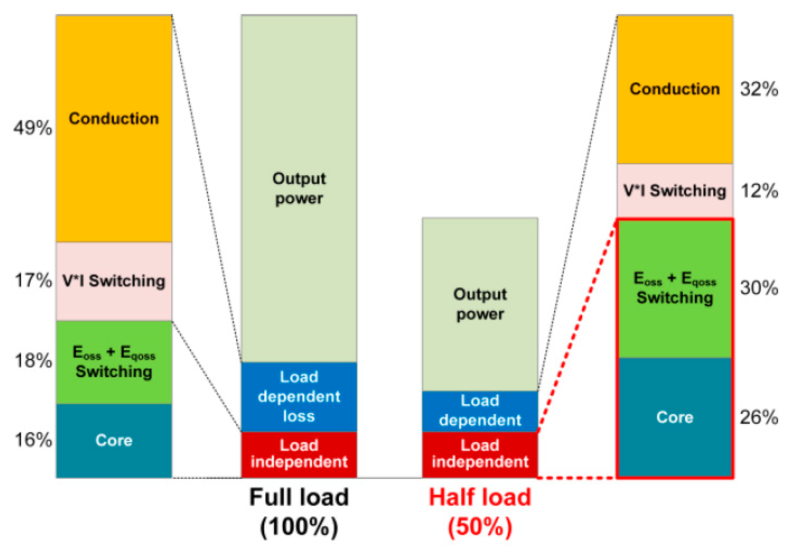
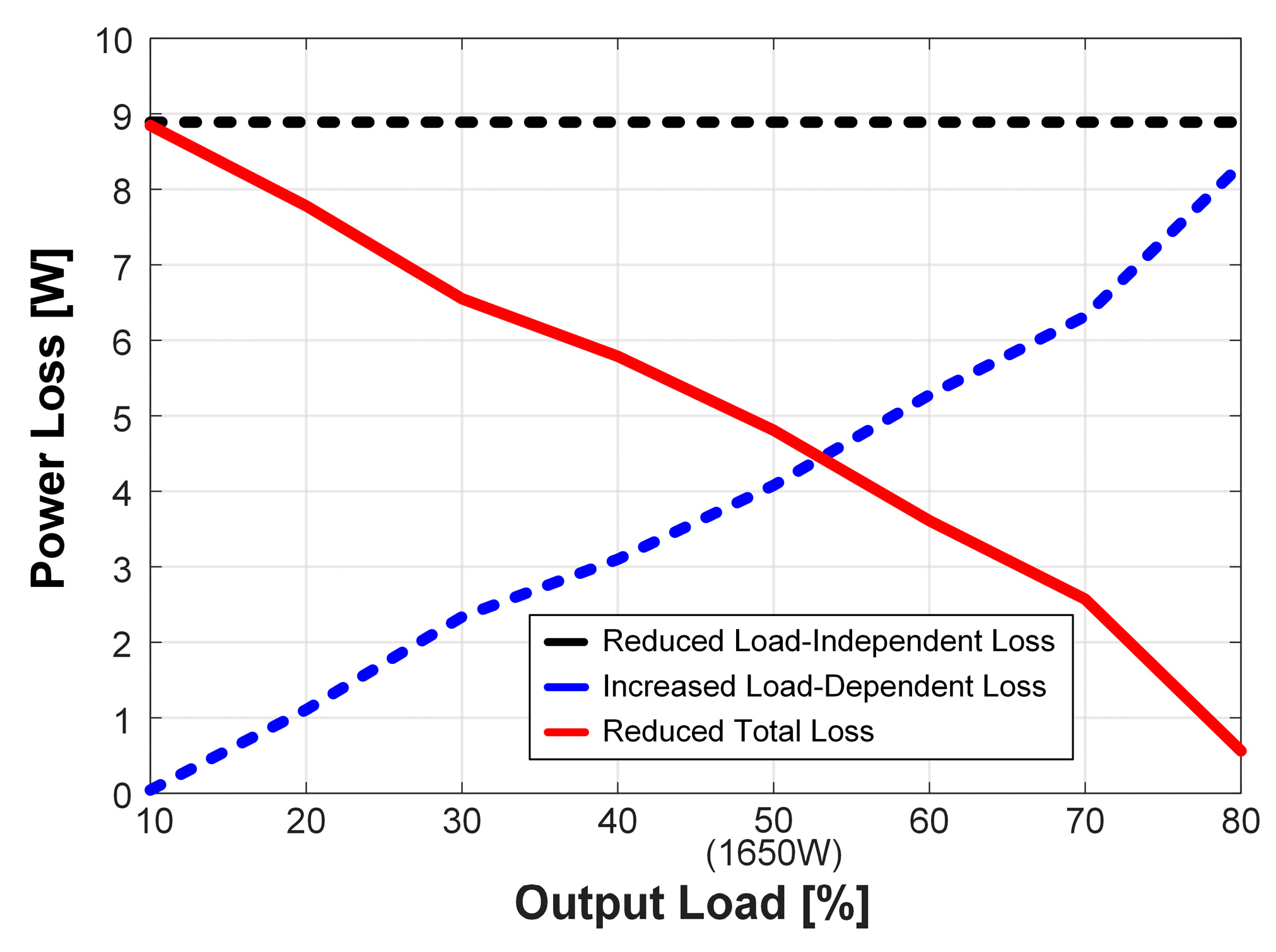
2.3. Analysis of Modifed PFC ON/OFF Control

This part presents power loss and power quality analysis of the modified PFC ON/OFF control. Since the modified PFC ON/OFF control operates similar to the conventional interleaving control when the power is over PO-max/2, this part only focuses on comparing two methods when the output power is half or less.
The power loss of a converter can be generally classified into two types: (1) load-dependent loss and (2) load-independent loss. The load-dependent loss, such as conduction loss, occupies the major portion of the power loss at full power conditions. Thus, the interleaved totem-pole bridgeless converter should reduce the load-dependent loss by using a lower resistance of inductor windings and lower channel resistance of semiconductor devices to maximize the full-load efficiency. However, these designs increase the load-independent loss, such as capacitor charging losses (Eoss and Eqoss) of switches [20] and core loss, constituting a large portion of the power loss at half-load conditions, as shown in Figure 3. Consequently, the interleaved totem-pole bridgeless converter with the conventional interleaving control method is difficult to maximize both full-load and half-load efficiencies. The modified PFC ON/OFF control enables the converter to reduce the load-independent loss by half and maximize the half-load efficiency. The detail loss comparison is presented in this part based on a 3.3 kW prototype, which is a reduced scale prototype of the interleaved totem-pole bridgeless converter that is used for experimental verification. Detailed specifications and designed parameters are shown in Table 1.
Conduction loss of two diodes (DH and DL) is calculated as follows:
P C o n d , D = I I N A v g · V F · 2 ,
where VF is the forward voltage drop of a diode, and IIN−Avg is the average input current, which is the same in the modified PFC ON/OFF and conventional control methods assuming the same efficiency.
MOSFET and inductor conduction losses related to resistances are
P C o n d , R = R T A C 0 T A C i L B 2 ( t ) · D ( t ) d t ,
where TAC is a period of the AC line cycle, D(t) is the duty ratio of semiconductor devices (D(t) is 1 for inductor conduction loss), and R is the parasitic resistance such as channel resistance and inductor winding resistance. Since the modified PFC ON/OFF control and conventional control are adopted to the same prototype, they have the same R and D(t). Thus, the modified ON/OFF control has two times higher total conduction loss than the conventional scheme due to two times higher iLB.
The boost converter suffers from a typical hard-switching transition when a switch building up the inductor current is turned on. Thus, the output capacitor of the switch is self-discharged, generating Eoss loss. Meanwhile, a current charging the output capacitor of the other switch generates a current bump, which results in the Eqoss. Eoss and Eqoss can be calculated as follows:
E o s s = 0 V O P F C V d s · C o s s ( V d s ) d V d s ,
E q o s s = 0 V O P F C ( V O P F C V d s ) · C o s s ( V d s ) d V d s
where Vds is the drain-to-source voltage of the switch building up the inductor current and Coss is the output capacitance of the switch depending on Vds. From (3) and (4), since the power losses of Eoss and Eqoss are only a function of Vds and Coss, they are the load-independent loss.
The boost inductor core loss can be calculated by the Improved Generalized Steinmetz Equation (IGSE) [21]. Since two half-line cycles are symmetric, the core loss based on the IGSE can be expressed as follows:
P C o r e = 2 V C T A C 0 T A C / 2 k i | d B ( t ) d t | α ( Δ B ) β α d t ,
where VC is the volume of a magnetic core, dB(t)/dt is the rate of change of flux density, α and β are original Steinmetz equation coefficients determined by the material characteristics, and ki is the coefficient shown below
k i = K ( 2 π ) α 1 0 2 π | c o s θ | α 2 β α d θ ,
where K is an original Steinmetz equation coefficient.
Figure 4 shows the power loss comparison between the modified PFC ON/OFF control and conventional interleaving control based on (1)–(5) and the designed parameters of Table 1. The modified PFC ON/OFF control alternatively uses one of two modules during the half AC line cycle, which makes both advantages and disadvantages in terms of the power loss. Since only one module handles total output power, the modified PFC ON/OFF control increases the output current of each module by two times of the conventional interleaving control. Thus, as the output power increases, the load-dependent loss is increased compared to the conventional interleaving control. On the other hand, the modified PFC ON/OFF control reduces the load-independent loss by half (9 W). When the converter is designed with lower channel resistance and winding resistance to maximize the full-load efficiency, the modified PFC ON/OFF control can improve the efficiency up to 80% load condition. However, since the maximum output current of each module should be designed to be the same with the conventional control, the modified PFC ON/OFF control can be applied to a 50% or less load condition.
Meanwhile, a simple control, which always turns off one of two modules at 50% or less load condition, can be considered to optimize both the half and full-load efficiencies. However, since this control only uses a module to deliver total power, the operating module suffers from its highest temperature stress even at the half-load condition. Due to the module, more cooling energy is required, and the lifetime of the OBC can be shortened. The modified PFC ON/OFF control enables two modules not only to operate at their optimized load condition in the same manner as the simple control but also to share the output power in the same manner as the conventional interleaving control. As a result, the modified PFC ON/OFF control can achieve higher efficiency than the conventional interleaving control and achieve better thermal performance than the simple one module operation control.
The modified PFC ON/OFF control can also improve the power quality, such as power factor (PF) and total harmonic distortion (THD), compared to the conventional interleaving control at 50% or less load condition. When the average current control is applied to the boost PFC converter, the PF and THD are degraded as the load decreases. This is because the boost PFC converter operates under the DCM (discontinuous conduction mode) region in the light load condition, resulting in current distortion in the DCM region and DCM–CCM transition instant [22]. Based on this characteristic, since the conventional interleaving control makes the PFC converter operate in relatively low load conditions by sharing the load current, it shows a relatively large current distortion in the light load conditions causing low PF and high THD. This tendency appears more and more as the load decreases. Meanwhile, the PFC converter adopting the single phase control and modified PFC ON/OFF control operates more heavy load conditions than the PFC adopting the interleaving control, which can reduce the current distortion resulting from the operation at the DCM and DCM–CCM transition instant. As a result, the modified PFC ON/OFF control can provide low current distortion with high PF and low THD compared to the conventional interleaving control.

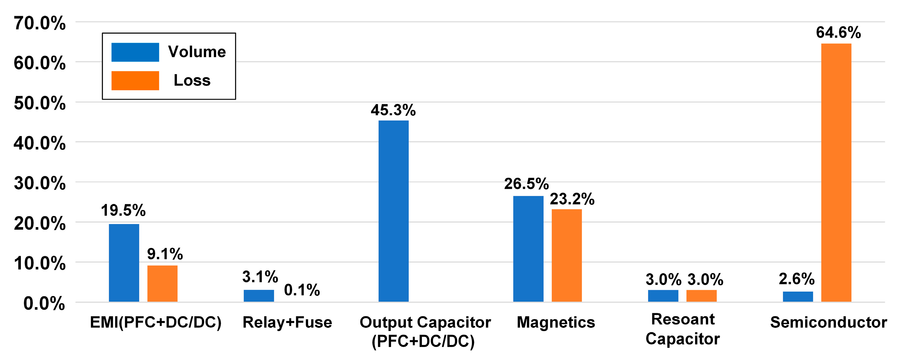
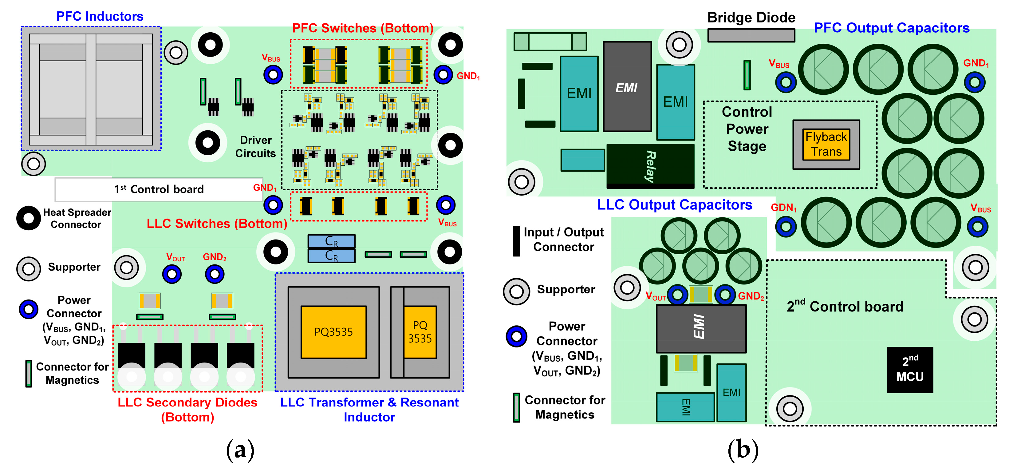
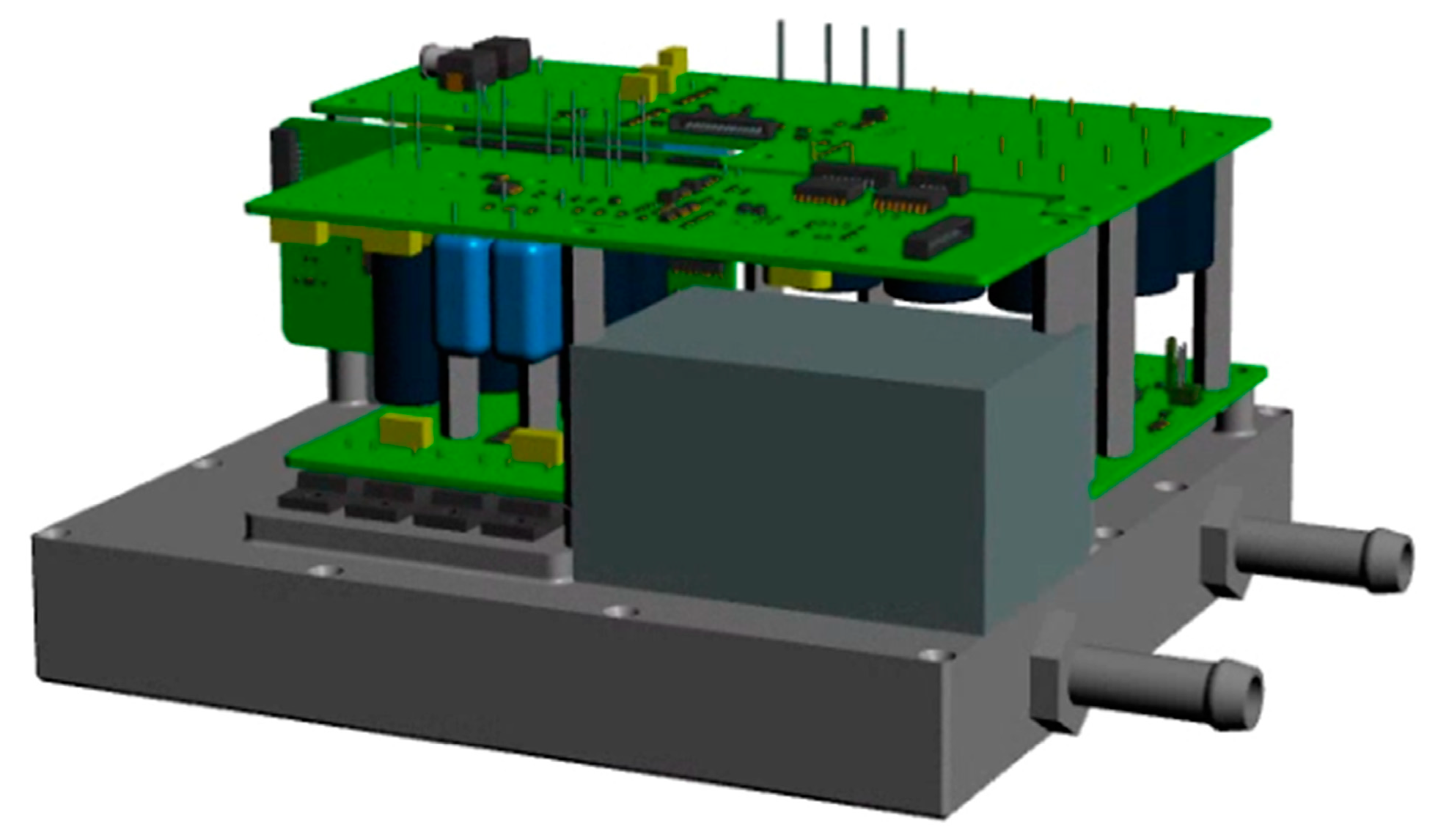
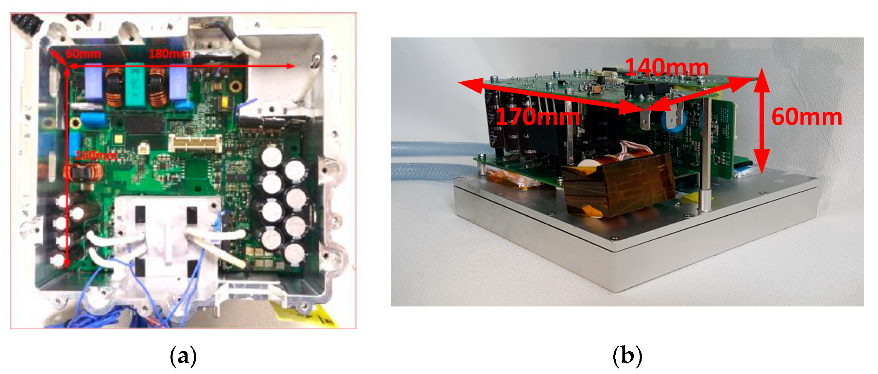
3. D-PCB Design for High-Power Density OBC

In order to develop a high-power density OBC, not only good topology and control but also well designed PCB is critical. An inappropriate PCB design easily deteriorates the power density and efficiency. It is general to place all components on a two-dimensional (2D) top and bottom area of a PCB board [23,24]. The 2D-PCB design is simple because it has only one PCB board. However, the 2D-PCB design has a limitation in achieving higher power density. Figure 5 shows the volume and power loss distribution of main components of the 3.3 kW prototype presented in this paper. The prototype is composed of an interleaved totem-pole bridgeless boost PFC converter and full-bridge LLC resonant converter. Table 1 and Table 2 show designed parameters. From Figure 5, electrolytic output capacitors of the PFC and DC-DC stages occupy around 50% of total volume while causing almost 0% power loss. On the other hand, semiconductor devices such as a switch and diode occupy about 3% volume but cause over 60% power loss. To cover high power loss with small volume, semiconductor devices necessarily need heat spreaders. Magnetic components such as boost inductors and transformers also generate large power loss and require heat spreaders. In 2D design, since all components are on the same board, there is a trade-off relationship between the PCB trace design and heat spreader design. If devices causing large power loss, such as semiconductor devices and magnetic components, are placed close to each other to design heat spreaders effectively, it increases the length of PCB power traces from semiconductor devices to other components, resulting in large PCB conduction loss. On the other hand, if the PCB power trace is designed for the shortest path, the heat spreader design cannot be optimized and requires a special shape and high cost. Above all, putting all the components in a PCB board increases the PCB area, thereby resulting in low power density due to a high height of electrolytic capacitors.
This paper presents a three-dimensional (3D) PCB design not only to improve the power density of the OBC but also simplify the heat spreader design for semiconductor devices and magnetics. The 3D-PCB design is composed of two PCB boards shown in Figure 6. One PCB board (bottom board) is for components generating larger power loss and requiring heat spreaders. In Figure 6a, all semiconductor devices are on the bottom layer of the board to directly transfer heat to the heat spreader, which is located underneath the bottom board. The magnetics of the OBC can also dissipate their heat to the heat spreader directly. The heat spreader connectors link the bottom PCB and heat spreader mechanically. Figure 6b shows the top board of the 3D-PCB design. This board (top board) is over the bottom board and consists of components with a large size but nearly small power loss, such as a relay, output capacitors, and EMI filter. Power connectors link the bottom and top boards electrically through conductive copper rods, and the copper rods and supporters shore up the weight of the top board. All connectors should be designed to use a screw for meeting the vibration requirements of the OBC. The 3D-PCB design can decouple the relationship between the PCB trace design and heat spreader design by separating the lossy and bulky parts. The height of the prototype is determined by electrolytic capacitors such as the 2D-PCB design. However, since a 3D design can have a smaller 2D area of the PCB board than a 2D design, it can improve the power density compared to a 2D-PCB design. Figure 7 shows a 3D assembly drawing of the 3.3 kW prototype with a heat spreader.

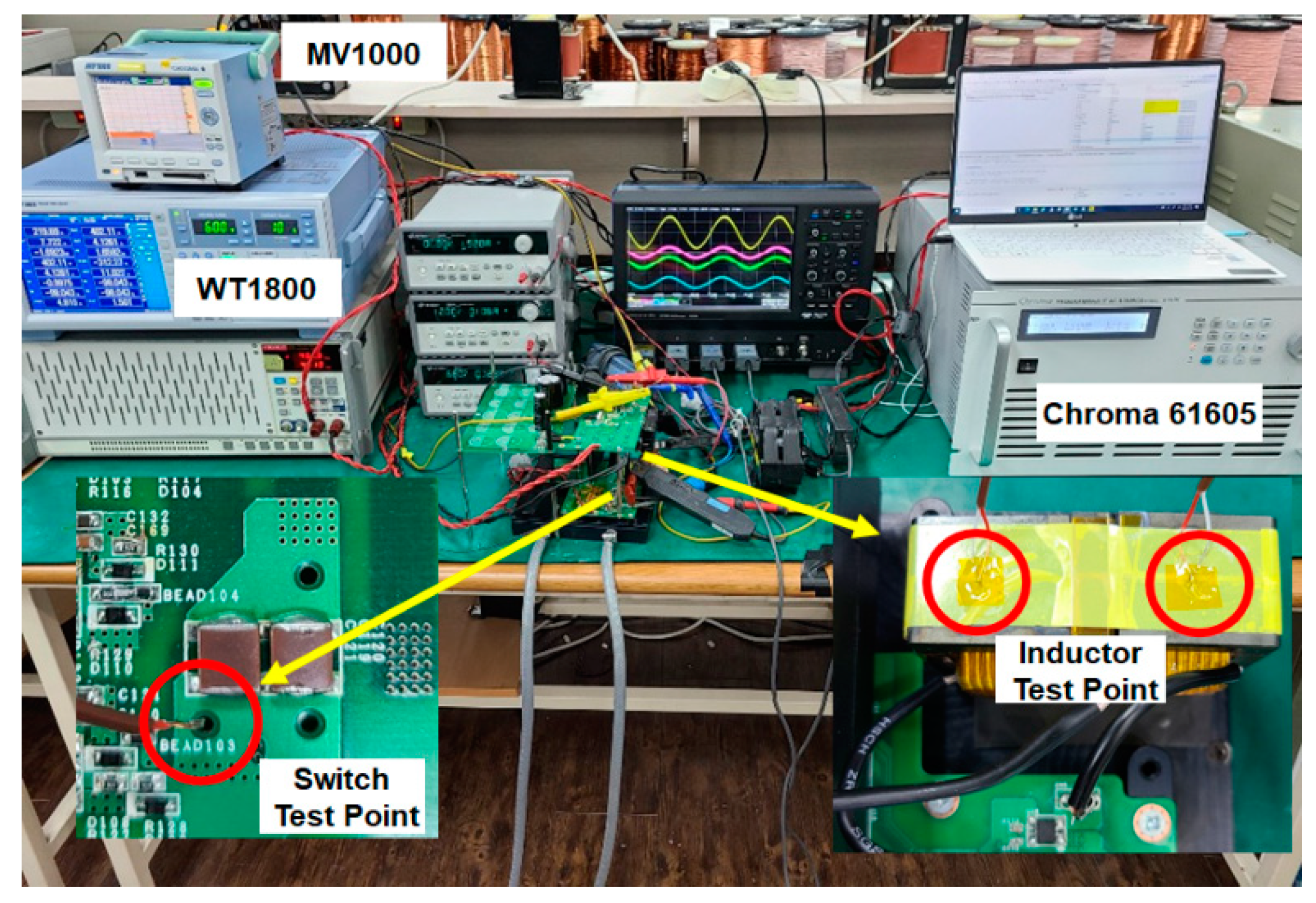
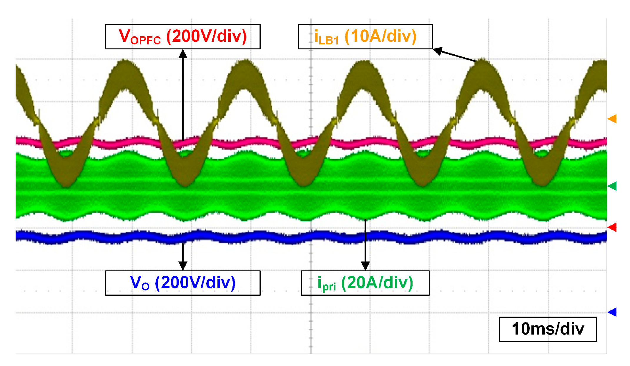
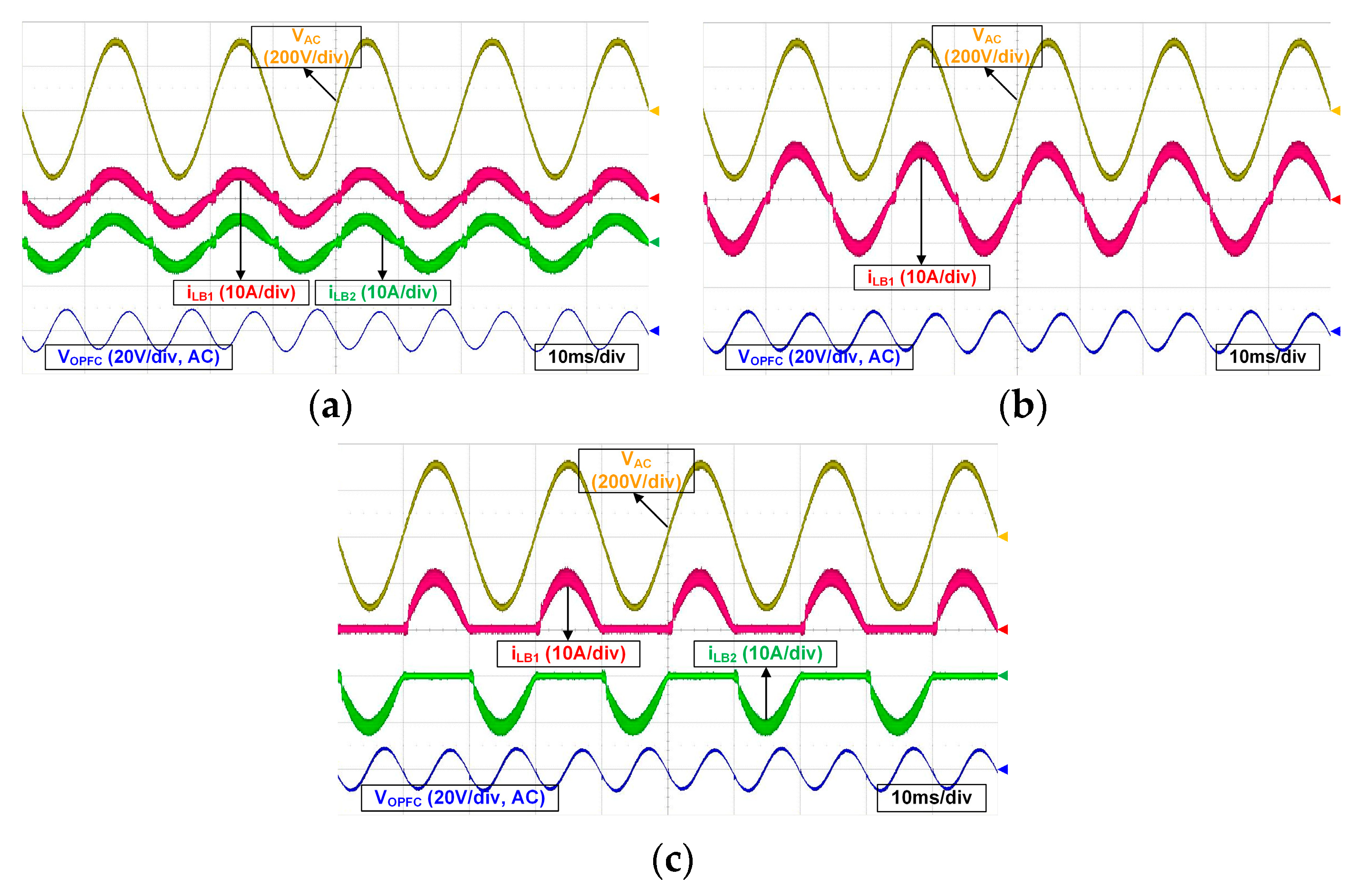
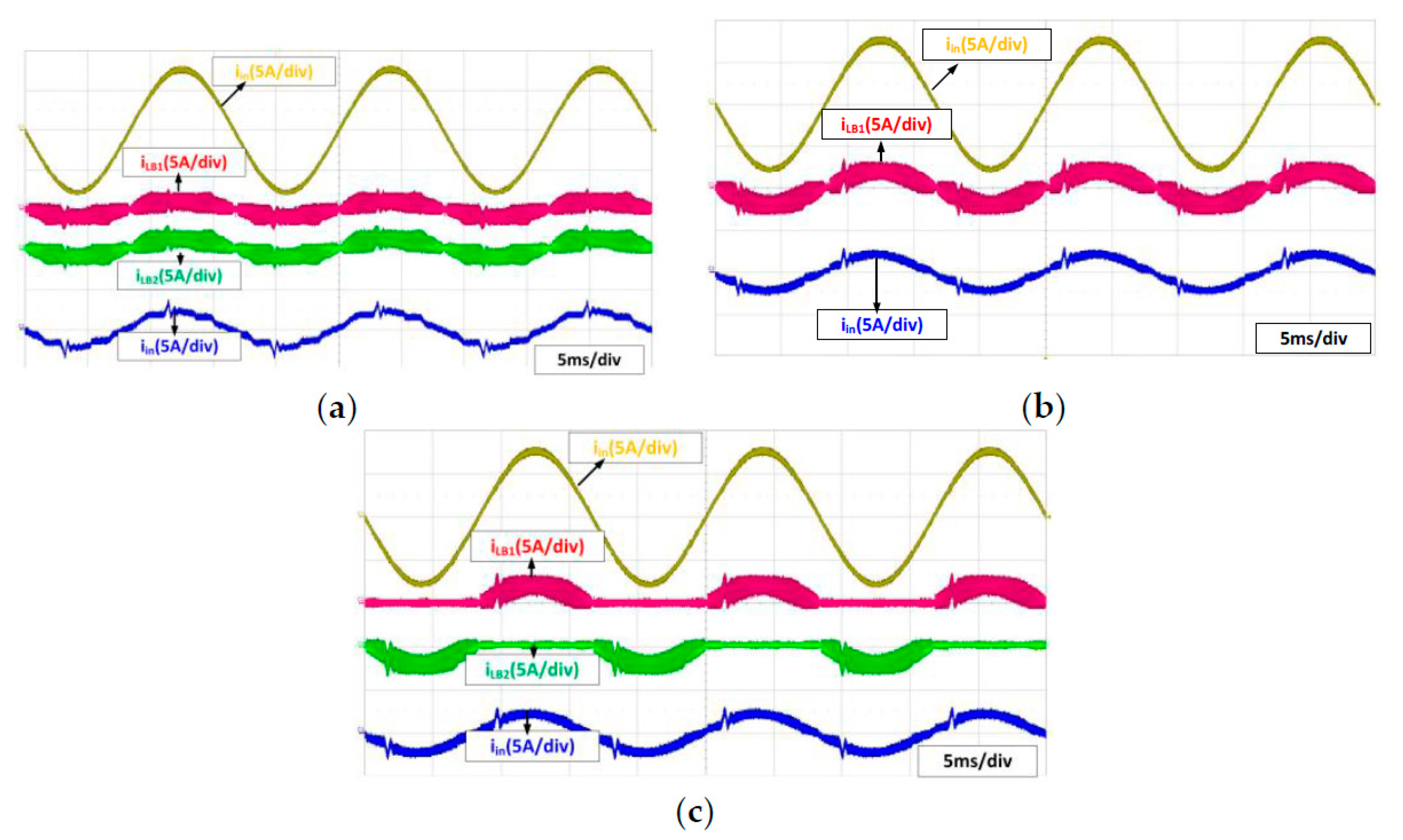
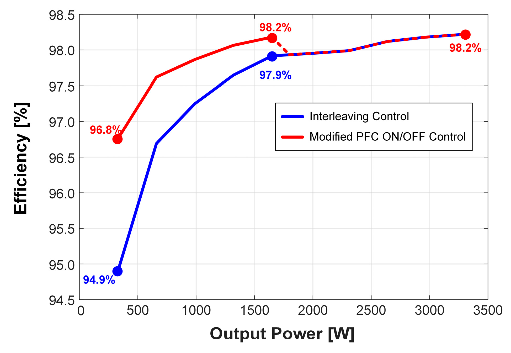
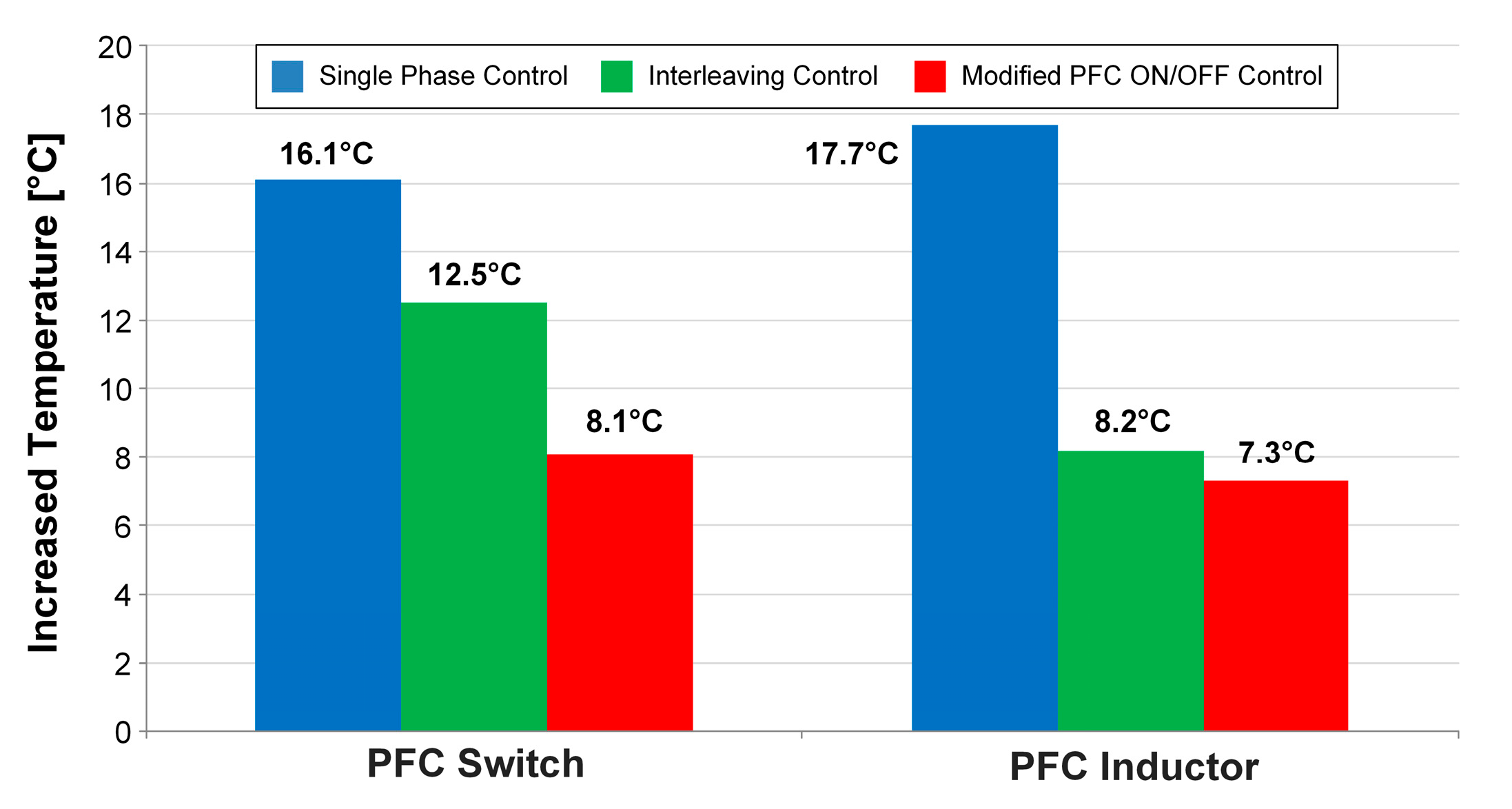
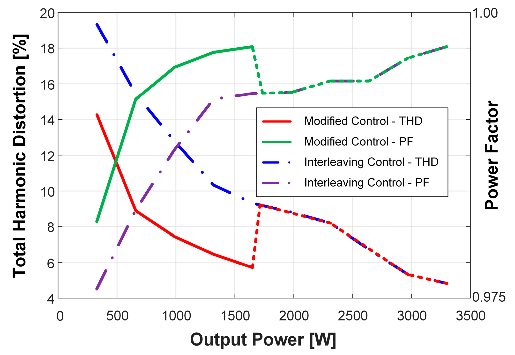
4. Experimental Results

To verify the effectiveness of the modified PFC ON/OFF control and 3D-PCB design, a 3.3 kW prototype with 220 Vrms AC input and 360 V/9.17 A output was built and tested. The topology and control block diagram of the prototype is shown in Figure 8. Table 1 and Table 2 summarize the details of the prototype. Figure 9 shows a picture of conventional commercial OBC and proposed prototype. The power density of the prototype is 2.3 kW/ℓ without a liquid cooling system and case, and this power density is almost 20% higher than that of the conventional commercial 3.3 kW OBC (1.9 kw/ℓ). Figure 10 shows the experimental platform and temperature test point of the PFC switch and inductors.
Figure 11 shows the captured waveforms of the prototype at full-load condition where the modified PFC ON/OFF control is inactive and conventional interleaving control is used. The PFC stage regulates the input current shape and its output voltage. The full-bridge (FB) LLC converter regulates the output voltage as 360 V. Figure 12 shows the captured waveforms of the PFC stage with different control methods at 50% load condition. The conventional interleaving control enables two boost modules to share the output power. Thus, it has the lowest inductor current. The single phase control only uses one module. Thus, it has two times higher inductor current than the interleaving control. In the modified PFC ON/OFF control, two boost modules operate alternately without any current distortion, and inductor current stress is the same as the single-phase control case.
Figure 13 presents the experimental waveforms in 10% load conditions. The conventional interleaving control method operates almost in DCM in 10% load condition, and large current distortion is induced by dynamic change between CCM and DCM operations. Meanwhile, single-phase control and modified PFC ON/OFF control show relatively low current distortion, since those control methods have two times higher inductor currents than the conventional interleaving method. In addition, single-phase control and modified PFC ON/OFF control mostly operate in CCM. Thus, the modified PFC ON/OFF control can provide lower THD than that of the conventional interleaving control method.
Figure 14 shows the measured efficiency of the PFC stage at 220 Vrms AC input and 400 V PFC output voltage. The efficiency was measured with a Yokogawa WT 1800. The modified PFC ON/OFF control is activated at 50% or less load condition. Thus, it has the same efficiency as the conventional interleaving control over 50% load condition, i.e., 1650 W. From 50% load condition, the modified control is active and improves the efficiency by reducing the load-independent losses, such as the capacitor charging loss of switches and core loss, as discussed in Section 2.3. Figure 15 shows the increased temperature of the PFC switch and inductor in three different PFC stage controls at 50% load condition. By alternately operating one of two modules, the modified PFC ON/OFF control much improves thermal performance, which can reduce the energy for cooling of the system. The prototype system efficiency, including the FB LLC converter, is 95.74% at full-load condition and 96.23% at half-load condition.
Figure 16 shows the power quality of the PFC stage. The proposed modified PFC ON/OFF control provides higher PF and lower THD than the conventional interleaving control. Since the proposed modified control operates under twice lager load conditions than the conventional interleaving control method, the PFC converter with the proposed control operates in CCM even under light load conditions, which minimizes the current distortion resulting from the dynamics change between CCM and DCM and current oscillation in DCM [21]. As a result, the modified PFC ON/OFF control efficiently reduces the current distortion and achieves higher power quality.

5. Conclusions

This paper presents the modified PFC ON/OFF control and 3D-PCB design to improve the efficiency and power density of OBCs without any additional components and complex control schemes. The modified PFC ON/OFF control uses one of two boost PFC modules alternately at 50% or less load condition to reduce load-independent power loss. It allows the OBC to maintain high efficiency both at full load and half-load conditions. Moreover, it can improve power quality and thermal performance compared to conventional interleaving control and single phase control. The 3D-PCB design that uses two PCBs to decouple the relationship between the PCB trace optimization design and the heat spreader design is presented. The 3D-PCB design can decrease the PCB area and improve power density effectively. These methods can be applied to any OBC comprising interleaved PFC topologies and DC-DC topologies. A 3.3 kW prototype was built and tested to verify the effectiveness of the proposed methods, but the proposed methods can also be applied to higher power level.

Author Contributions

J.B. and H.-S.Y. were the main researchers who initiated and organized research reported in the paper, all authors including M.-H.P. and T.K. was responsible for making the prototype of the proposed system and carrying out the experiment. All authors have read and agreed to the published version of the manuscript.

Funding

National Research Foundation of Korea: 2020R1C1C1010268. Korea Agency for Infrastructure Technology Advancement: 20CTAP-C157058-01.

Acknowledgments

This work was supported by the National Research Foundation of Korea (NRF) grant funded by the Korea government (MSIT) (No. 2020R1C1C1010268). This work is supported by the Korea Agency for Infrastructure Technology Advancement (KAIA) grant funded by the Ministry of Land, Infrastructure and Transport (Grant 20CTAP-C157058-01).

Conflicts of Interest

The authors declare not conflict of interest.

References

  1. Greenhouse Gas Emissions from a Typical Passenger Vehicle. Available online: https://www.epa.gov-/greenvehicles/greenhousegas-emissions-typical-passenger-vehicle (accessed on 31 March 2018).
  2. CO2 Emission Standards for Passenger Cars and LightCommercial Vehicles in the European Union. Available online: https://theicct.org/publications/ldv-co2-stds-eu-2030-update-jan2019 (accessed on 31 January 2019).
  3. Global EV Outlook 2019. May 2019. Available online: https://www.iea.org/reports/global-ev-outlook-2019 (accessed on 15 February 2020).
  4. Shen, Y.; Zhao, W.; Chen, Z.; Cai, C. Full-Bridge LLC Resonant Converter With Series-Parallel Connected Transformers for Electric Vehicle On-Board Charger. IEEE Access 2018, 6, 13490–13500. [Google Scholar] [CrossRef]
  5. Lim, C.-Y.; Moon, G.W. Phase-Shifted Full-Bridge DC-DC Converter with High Efficiency and High Power Density Using CenterTapped Clamp Circuit for Battery Charging in Electric Vehicles. IEEE Trans. Power Electron. 2019, 34, 10945–10959. [Google Scholar] [CrossRef]
  6. Patil, D.; Agarwal, V. Compact Onboard Single-Phase EV Battery Charger with Novel Low-Frequency Ripple Compensator and Optimum Filter Design. IEEE Trans. Vehicular Technol. 2016, 65, 1948–1956. [Google Scholar] [CrossRef]
  7. Lu, J.; Mallik, A.; Khaligh, A. Dynamic Strategy for Efficiency Estimation in a CCM-Operated Front-End PFC Converter for Electric Vehicle Onboard Charger. IEEE Trans. Transp. Electr. 2017, 3, 545–553. [Google Scholar] [CrossRef]
  8. Meher, S.R.; Banerjee, S.; Vankayalapati, B.T.; Singh, R.K. A Reconfigurable On-Board Power Converter for Electric Vehicle with Reduced Switch Count. IEEE Trans. Veh. Technol. 2020, 60, 3760–3772. [Google Scholar] [CrossRef]
  9. Zhang, Z.; Liu, C.; Wang, M.; Si, Y.; Lie, Y.; Lei, Q. HighEfficiency High-Power-Density CLLC Resonant Converter with LowStray-Capacitance and Well-Heat-Dissipated Planar Transformer for EV On-Board Charger. IEEE Trans. Power Electron. 2020, 35, 10831–10851. [Google Scholar] [CrossRef]
  10. Huber, L.; Jang, Y.; Jovanovic, M. Performance Evaluation of Bridgeless PFC Boost Rectifiers. IEEE Trans. Power Electron. 2008, 23, 1381–1390. [Google Scholar] [CrossRef]
  11. Liu, Z.; Lee, F.C.; Li, Q.; Yang, Y. Design of GaN-Based MHz TotemPole PFC Rectifier. IEEE J. Emerg. Sel. Top. Power Electron. 2016, 4, 799–807. [Google Scholar] [CrossRef]
  12. Fischer, G.S.; Rech, C.; de Novaes, Y.R. Extensions of LeadingEdge Modulated One-Cycle Control for Totem-Pole Bridgeless Rectifiers. IEEE Trans. Power Electron. 2020, 35, 5447–5460. [Google Scholar] [CrossRef]
  13. Jeong, Y.; Park, M.-H.; Moon, G.W. High-Efficiency Zero-VoltageSwitching Totem-Pole Bridgeless Rectifier with Integrated Inrush Current Limiter Circuit. IEEE Trans. Ind. Electron. 2020, 67, 7421–7429. [Google Scholar] [CrossRef]
  14. Su, B.; Lu, Z. An Interleaved Totem-Pole Boost Bridgeless Rectifier with Reduced Reverse-Recovery Problems For Power Factor Correction. IEEE Trans. Power Electron. 2010, 25, 1406–1415. [Google Scholar]
  15. Park, M.-H.; Baek, J.; Jeong, Y.; Moon, G.W. An Interleaved TotemPole Bridgeless Boost PFC Converter with Soft-Switching Capability Adopting Phase-Shifting Control. IEEE Trans. Power Electron. 2019, 34, 10610–10618. [Google Scholar] [CrossRef]
  16. Belkamel, H.; Kim, H.; Choi, S. Interleaved Totem-Pole ZVS Converter Operating in CCM for Single-Stage Bidirectional AC-DC Conversion with High-Frequency Isolation. IEEE Trans. Power Electron. 2021, 36, 3486–3495. [Google Scholar] [CrossRef]
  17. International Electrotechnical Commission, IEC 61851-1:2017-02. Electric Vehicle Conductive Charging System-Part 1: General Requirements; International Electrotechnical Commission: Geneva, Switzerland, 2017. [Google Scholar]
  18. Hanauer, D. Mode 2 Charging-Testing and Certification for International Market Access. World Electr. Veh. J. 2018, 9, 26. [Google Scholar] [CrossRef] [Green Version]
  19. Youn, H.-S.; Lee, J.-B.; Baek, J.-I.; Moon, G.-W. A Digital Phase Leading Filter Current Compensation (PLFCC) Technique for CCM Boost PFC Converter to Improve PF in High Line Voltage and Light Load Conditions. IEEE Trans. Power Electron. 2016, 31, 6596–6606. [Google Scholar] [CrossRef]
  20. Youn, H.-S.; Park, J.-S.; Park, K.-B.; Baek, J.-I.; Moon, G.-W. A Digital Predictive Peak Current Control for Power Factor Correction with LowInput Current Distortion. IEEE Trans. Power Electron. 2016, 31, 900–912. [Google Scholar] [CrossRef]
  21. Villar, I.; Viscarret, U.; Otaduim, I.-E.; Rufer, A. Global Loss Evaluation Methods for Nonsinusoidally Fed Medium-Frequency Power Transformers. IEEE Trans. Ind. Electron. 2009, 56, 4132–4140. [Google Scholar] [CrossRef]
  22. Hou, R.; Lu, J.; Chen, D. Parasitic Capacitance Eqoss Loss Mechanism, Calculation, and Measurement in Hard-Switching for GaN HEMTs. In Proceedings of the 2018 IEEE Applied Power Electronics Conference and Exposition (APEC), San Antonio, TX, USA, 4–8 March 2018; pp. 919–924. [Google Scholar]
  23. Li, B.; Li, Q.; Lee, F.C.; Liu, Z.; Yang, Y. A High-Efficiency HighDensity Wide-Bandgap Device-Based Bidirectional On-Board Charger. IEEE J. Emerg. Sel. Top. Power Electron. 2018, 6, 1627–1636. [Google Scholar] [CrossRef]
  24. Li, H.; Zhang, Z.; Wang, S.; Tang, J.; Ren, X.; Chen, Q. A 300-kHz 6.6-kW Bidirectional LLC Onboard Charger. IEEE Trans. Ind. Electron. 2020, 67, 1435–1445. [Google Scholar] [CrossRef]
Figure 1. Conventional interleaved totem-pole bridgeless boost power factor correction (PFC) converter. (a) Circuit diagram with control blocks. (b) Key waveforms.
Energies 14 00605 g001
Figure 2. Modified PFC ON/OFF control for interleaved totem-pole bridgeless boost PFC converter. (a) Key control block diagram. (b) Key waveforms. During Case 2, the role of each module can be swapped every few AC line cycles to obtain symmetric operation.
Energies 14 00605 g002
Figure 3. Loss breakdown of the interleaved totem-pole bridgeless converter with the conventional interleaving control.
Energies 14 00605 g003
Figure 4. Loss comparison of the modified PFC ON/OFF control and conventional interleaving control at 400 V and 3.3 kW maximum PFC output.
Energies 14 00605 g004
Figure 5. Volume and power loss distribution of 3.3 kW prototype.
Energies 14 00605 g005
Figure 6. Layout of two PCBs for 3D-PCB design. (a) Bottom PCB for lossy components. (b) Top PCB for bulky components. The heat spreader is located underneath the bottom PCB to dissipate heat effectively.
Energies 14 00605 g006
Figure 7. Three-dimensional (3D) assembly drawing of the 3.3 kW onboard charger (OBC) prototype with a heat spreader. The system has two power boards. Lossy parts are on the bottom board and bulky parts are on the top board.
Energies 14 00605 g007
Figure 8. Circuit diagram and control block diagram of the prototype with two digital microcontroller (MCU).
Energies 14 00605 g008
Figure 9. Picture of 3.3 kW OBC. (a) Commercial 3.3 kW OBC. (b) Proposed 3.3 kW OBC.
Energies 14 00605 g009
Figure 10. Picture of the experimental platform.
Energies 14 00605 g010
Figure 11. Captured waveforms of the prototype at 100% load condition. The modified PFC ON/OFF control is inactive above 50% load condition.
Energies 14 00605 g011
Figure 12. Captured waveforms of the PFC stage at 50% load condition. (a) Conventional interleaving control. (b) Single phase control. (c) Modified PFC ON/OFF control. The modified PFC ON/OFF control uses two boost modules alternately. All controls have a similar PFC output voltage ripple.
Energies 14 00605 g012
Figure 13. Captured waveforms of the PFC stage at 10% load condition. (a) Conventional interleaving control. (b) Single phase control. (c) Modified PFC ON/OFF control.
Energies 14 00605 g013
Figure 14. Measured efficiency of the PFC stage with two controls. The FB LLC converter has the same efficiency regardless of the PFC control methods.
Energies 14 00605 g014
Figure 15. Increased temperature of PFC switch and inductor in three different control methods at 50% load condition. Initial temperature is 26 °C and 29 °C for switch and inductor, respectively.
Energies 14 00605 g015
Figure 16. Measured power quality of the PFC stage with two controls. The measured condition is the same with the efficiency case.
Energies 14 00605 g016
Table 1. Designed parameters of 3.3 kW interleaved totem-pole bridgeless boost PFC converter.
ItemsParameters
Input voltage, vAC220 Vrms
PFC output voltage, VO-PFC400 V
Output power, PO1.65 kW per module
Switching frequency, fS-PFC100 kHz
Switch, QH and QLGS66516T
Diode, DH and DLLL25XB60
Boost inductor, LB113 µH and EI4322 (KP50)
Table 2. Designed parameters of 3.3 kW full-bridge (FB) LLC resonant converter.
ItemsParameters
Input voltage, VO-PFC400 V
Output voltage, VO360 V
Output power, PO3.3 kW
Resonant frequency, fR-LLC500 kHz
Switch, Q1Q4GS66508T
Diode, DS1DS4SCS220AM
Transformer53 µH (Lm) and PQ3535 (KP50)
Transformer turns ratio19:16
Resonant inductor, LR9.32 µH and PQI3520 (KP50)
Publisher’s Note: MDPI stays neutral with regard to jurisdictional claims in published maps and institutional affiliations.

