
Embedding an Electrical System Real-Time Simulator with Floating-Point Arithmetic in a Field Programmable Gate Array


Abstract
:1. Introduction
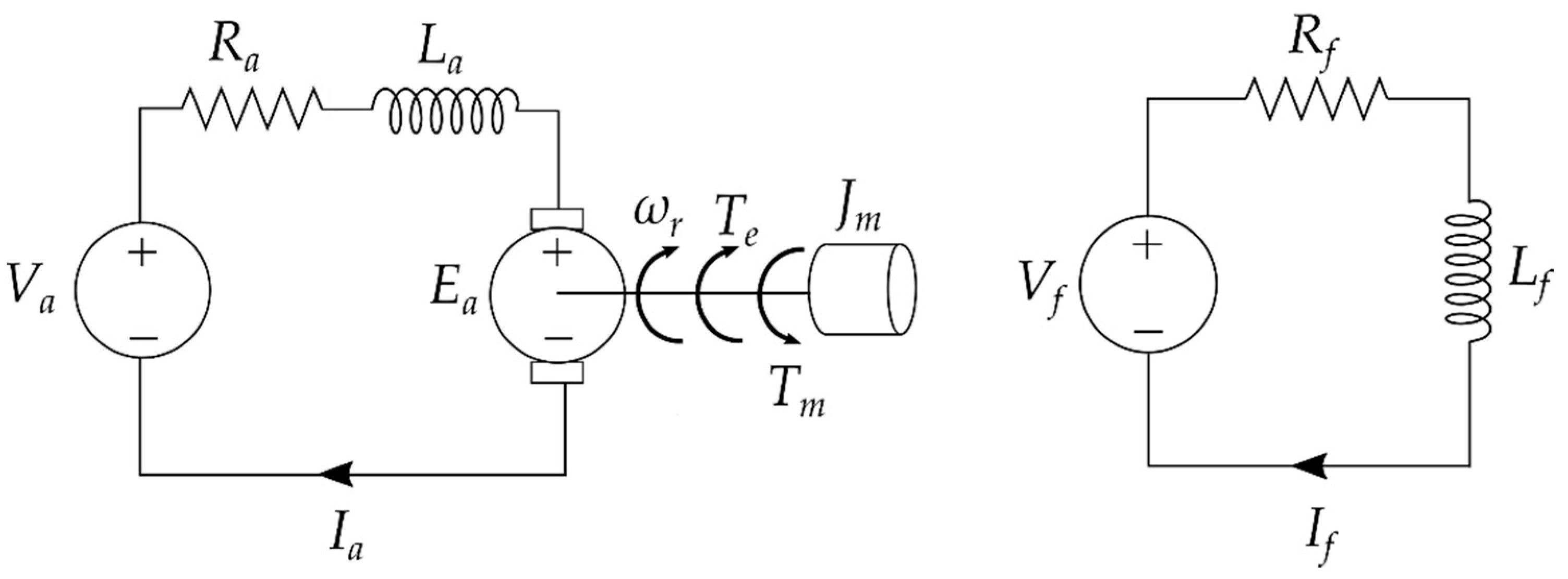
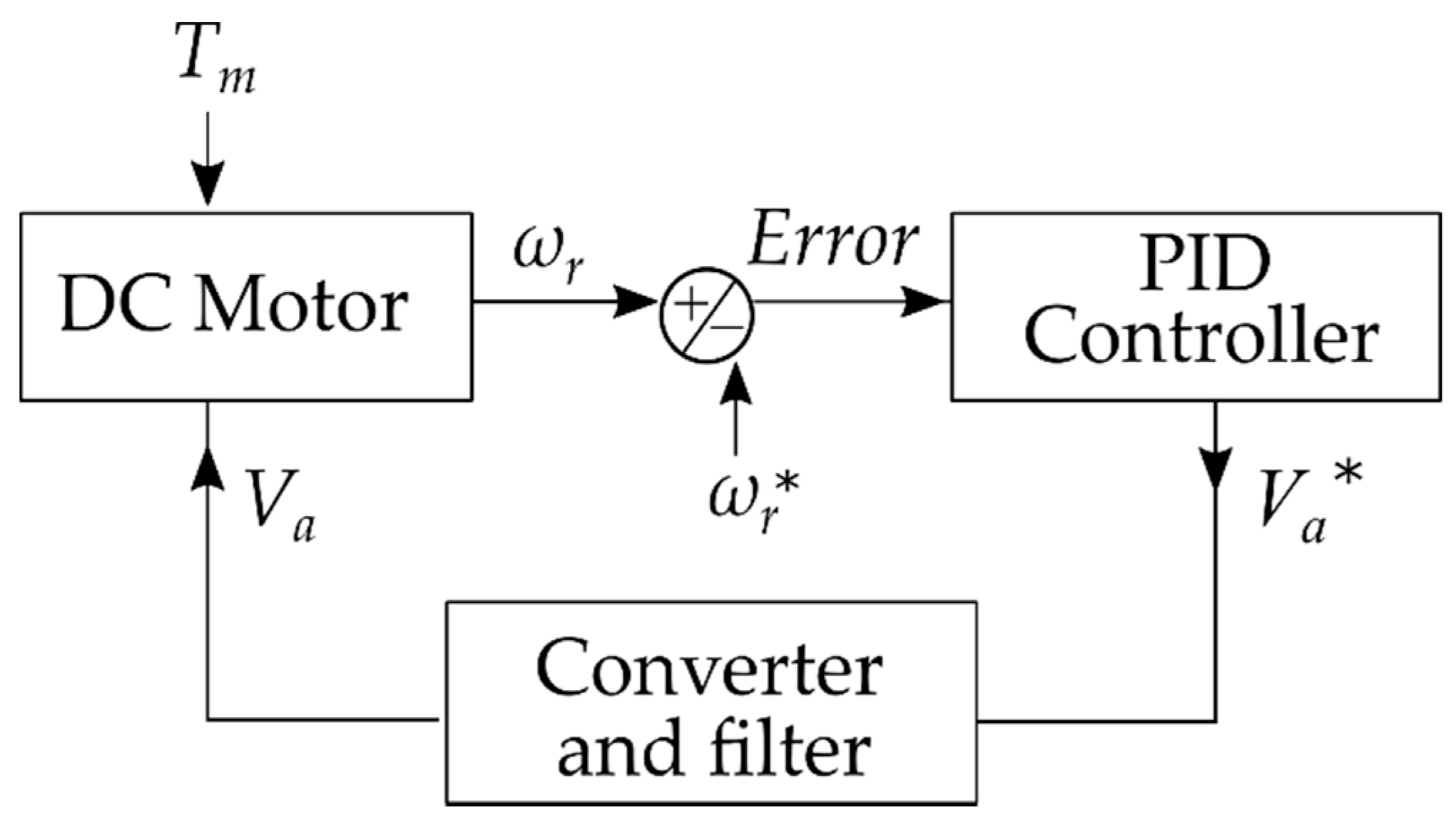
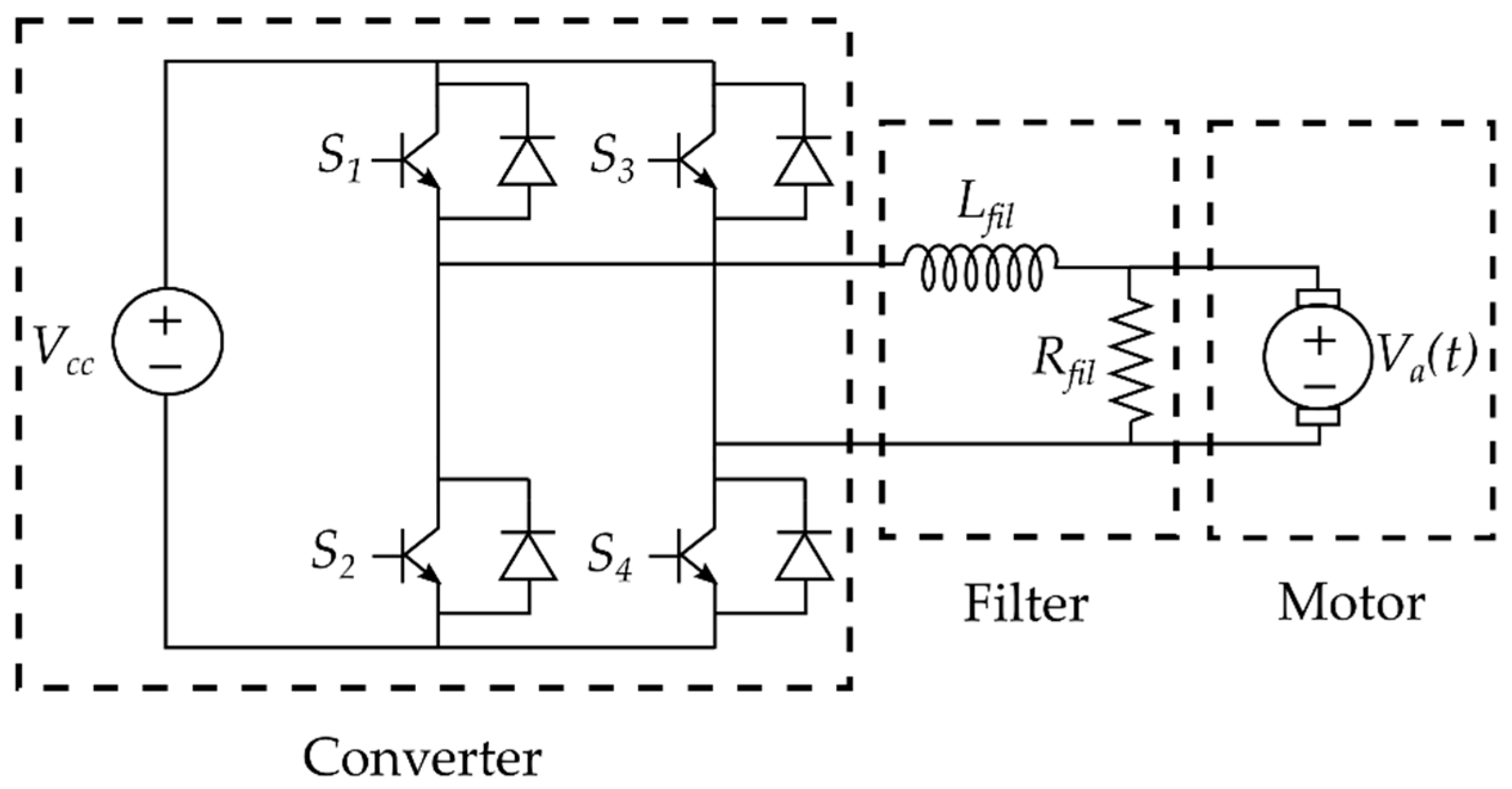
2. DC Motor Drive System Modelling
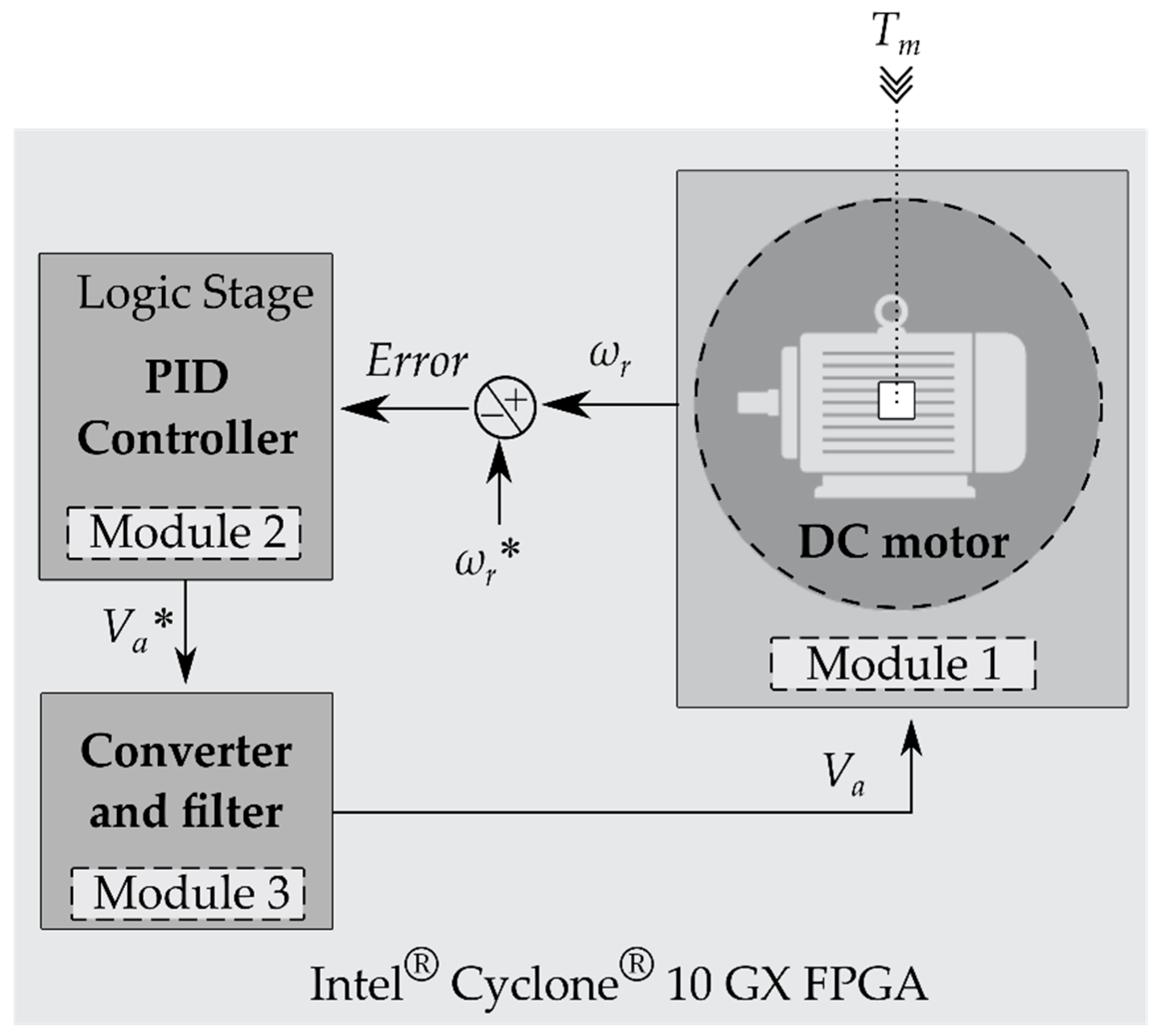
2.1. Model Description and Discretization
2.1.1. DC Motor
2.1.2. PID Controller
2.1.3. Power Converter
2.1.4. Filter
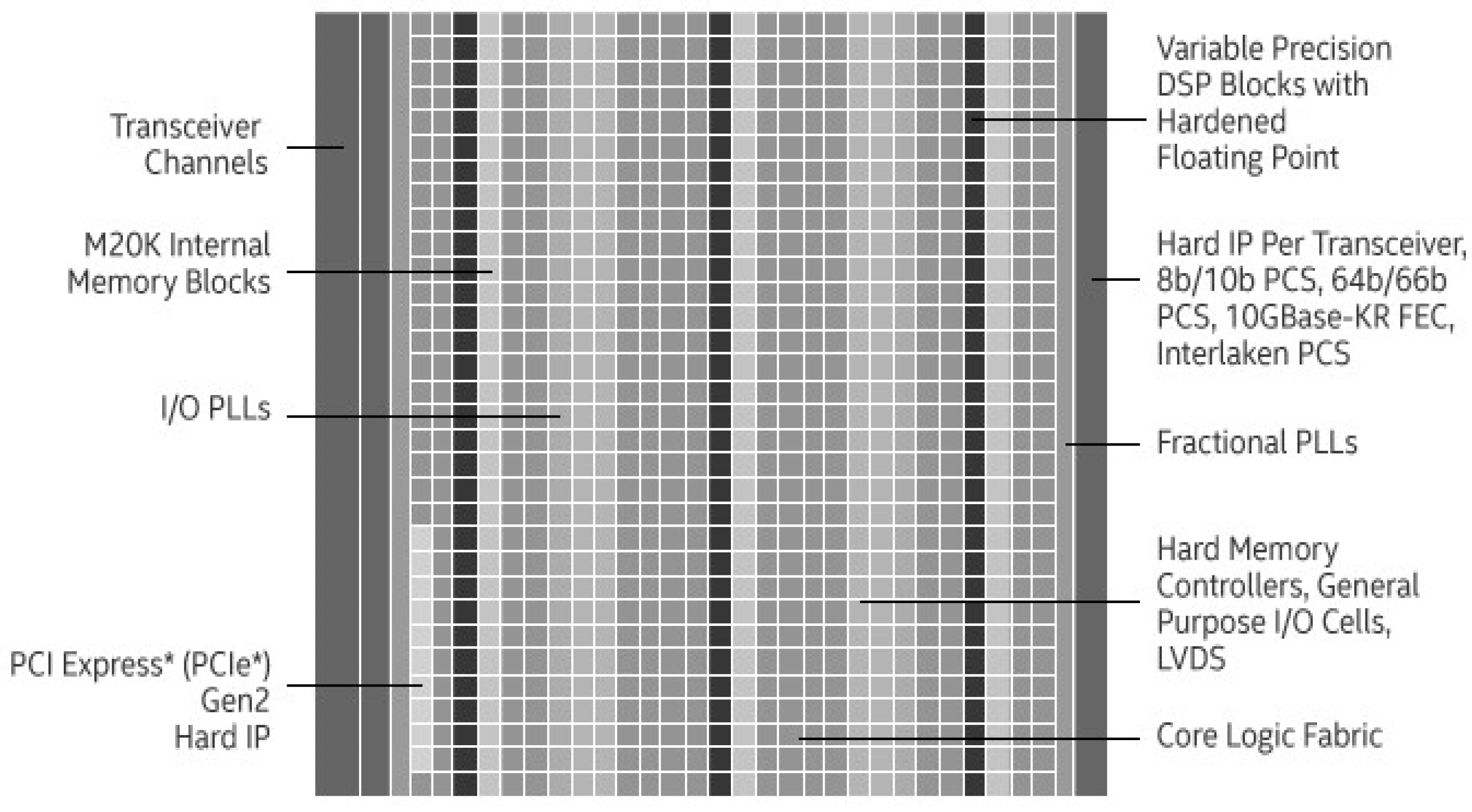
3. FPGA Features
3.1. FPGA Architecture
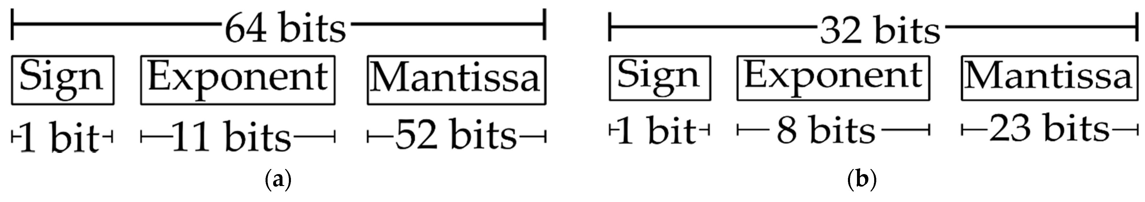
3.2. DPS—Floating-Point Precision
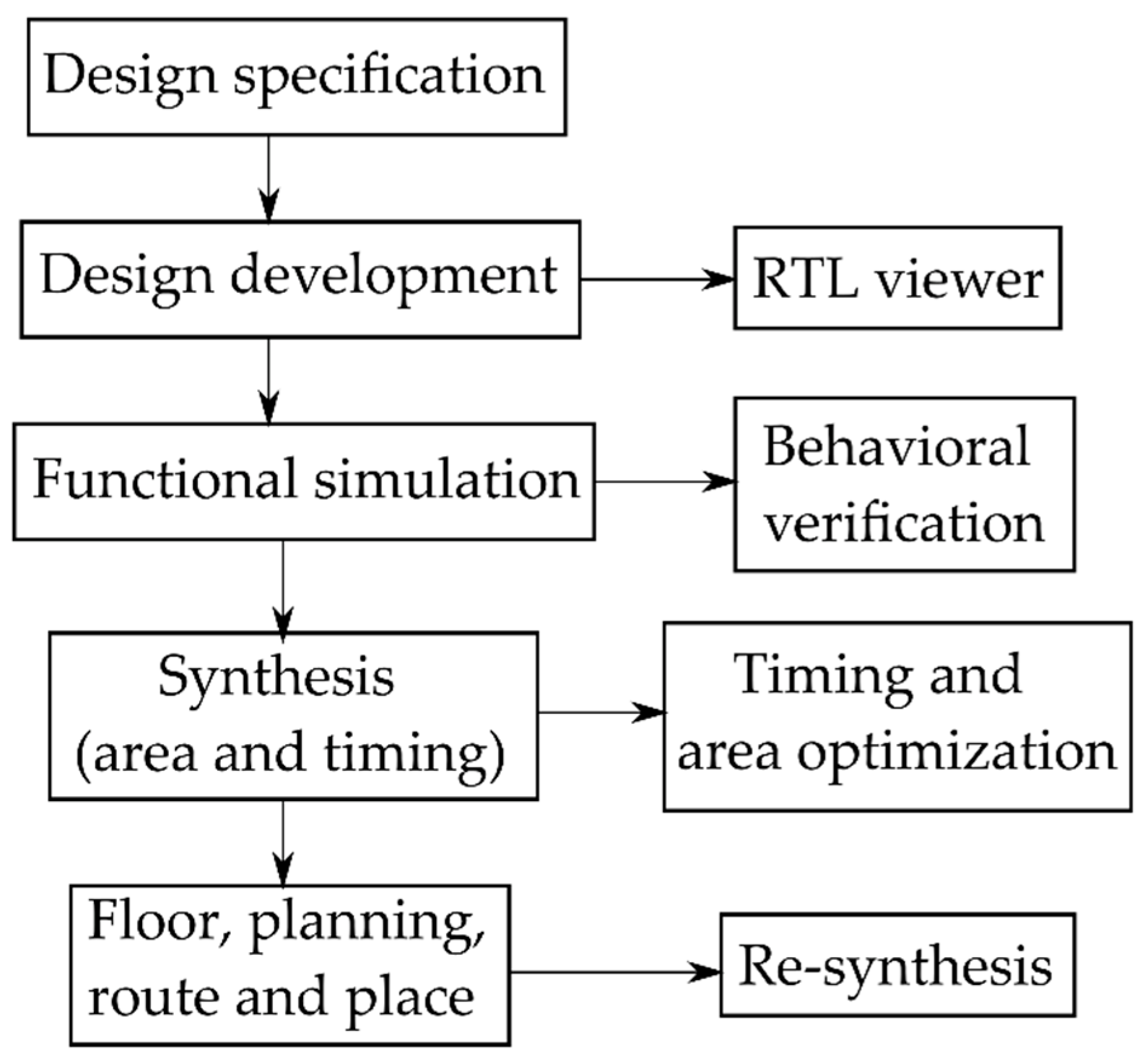
4. Hardware Development
5. Results and Discussion
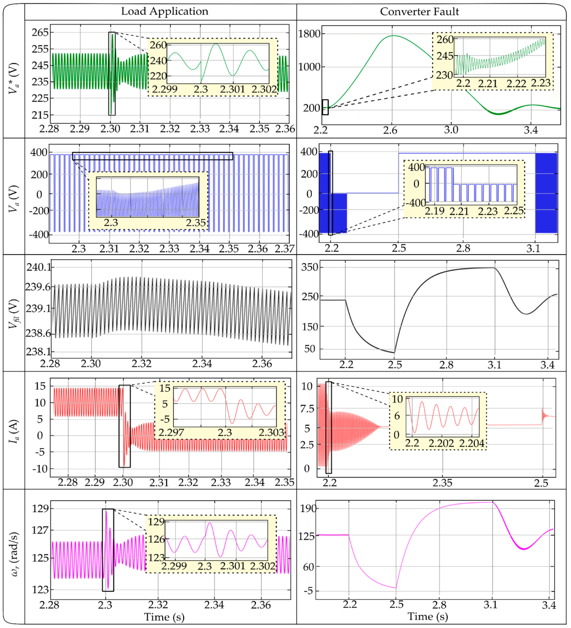
5.1. DC Motor Startup with Mechanical Load Followed by Load Withdrawal
- Settling time: 0.15 s;
- Overshoot: 3.1%.
5.2. Failure in the Converter Switching
5.3. Real-Time Simulation Performance
6. Conclusions
Author Contributions
Funding
Acknowledgments
Conflicts of Interest
Abbreviations
| CLB | Configurable logic block |
| DC | Direct Current |
| DSP | Digital Signal Processing |
| FPGA | Field-Programmable Gate Array |
| HDL | Hardware Description Language |
| HIL | Hardware-in-the-loop |
| IP | Intellectual Property |
| PMSG | Permanent Magnetic Synchronous Generator |
| PID | Proportional–Integrative–Derivative |
| PWM | Pulse-width Modulation |
| RT | Real-time |
| RTDS | Real-Time Digital Simulation |
| TB | Testbench |
References
- Hsiung, P.-A.; Santambrogio, M.D.; Huang, C.-H. Introduction to Reconfigurable Computing. In Reconfigurable System Design and Verification, 1st ed.; CRC Press: Boca Raton, FL, USA, 2009; Chapter 1, Section 1.7.4; p. 26. [Google Scholar]
- Faruke, M.O.; Strasser, T.; Lauss, G.; Jalili-Marandi, V.; Forsyth, P.; Dufour, C.; Paolone, M. Real-Time Simulation Technologies for Power Systems Design, Testing, and Analysis. IEEE Power Energy Technol. Syst. J. 2015, 2, 63–73. [Google Scholar]
- Guillaud, X.; Faruque, M.O.; Teninge, A.; Hariri, A.H.; Vanfretti, L.; Paolone, M.; Davoudi, A. Applications of Real-Time Simulation Technologies in Power and Energy Systems. IEEE Power Energy Technol. Syst. J. 2015, 2, 103–115. [Google Scholar] [CrossRef] [Green Version]
- Iracheta-Cortez, R.; Flores-Guzman, N. Developing automated Hardware-In-the-Loop tests with RTDS for verifying the protective relay performance. In Proceedings of the 2016 IEEE 36th Central American and Panama Convention (CONCAPAN XXXVI), San José, Costa Rica, 9–11 November 2016. [Google Scholar]
- RTDS Technologies—Simulation Hardware: Scalability and Flexibility without Performance Loss. Available online: https://www.rtds.com/technology/simulation-hardware/ (accessed on 8 October 2021).
- OPAL-RT Technologies: Simulator Op5707XG. Available online: https://www.rtds.com/technology/simulation-hardware/ (accessed on 8 October 2021).
- OPAL-RT Technologies: System eMEGASIM. Available online: https://www.opal-rt.com/system-emegasim/ (accessed on 8 October 2021).
- OPAL-RT Technologies: System Hypersim. Available online: https://www.opal-rt.com/system-hypersim/ (accessed on 8 October 2021).
- Amin, M.; Rehmani, M.H. Operation, Construction, and Functionality of Direct Current Machines; IGI Global: Hershey, PI, USA, 2015; pp. 1–56. [Google Scholar]
- Grégoire, L.-A.; Vian, J.; Cense, S.; Belanger, J. Real-time simulation of an asymmetrical phase domain synchronous machine on FPGA. In Proceedings of the IEEE 12th International Conference on Power Electronics and Drive Systems, Honolulu, HI, USA, 12–15 December 2017; pp. 659–664. [Google Scholar]
- Rama, D.; Ananthan, T. FPGA Based Emulator Design of a DC Motor. In Proceedings of the International Conference on Communication and Electronics Systems, Coimbatore, India, 17–19 July 2019. [Google Scholar]
- Liu, Q.; Gao, M.; Zhang, Q. Knowledge-Based Neural Network Model for FPGA Logical Architecture Development. IEEE Trans. Very Large Scale Integr. (VLSI) Syst. 2015, 24, 1. [Google Scholar] [CrossRef]
- Farooq, U.; Baig, I.; Alzahrani, B.A. An Efficient Inter-FPGA Routing Exploration Environment for Multi-FPGA Systems. IEEE Access 2018, 6, 56301–56310. [Google Scholar] [CrossRef]
- Inacio, C.; Ombres, D. The DSP decision: Fixed point or floating? IEEE Spectr. 1996, 33, 72–74. [Google Scholar] [CrossRef]
- Intel® Cyclone® 10 GX FPGA Features. Intel® Cyclone®. Available online: https://www.intel.com/content/www/us/en/products/details/fpga/cyclone/10/gx/article.html (accessed on 10 October 2021).
- Intel®. (2018, August). Intel® Cyclone® 10 GX FPGA Development Kit User Guide. Intel® Cyclone®, User Guide. Available online: https://www.intel.com/content/dam/www/programmable/us/en/pdfs/literature/ug/ug-c10-gx-fpga-devl-kit.pdf (accessed on 8 October 2021).
- IEEE Computer Society. IEEE Standard for Binary Floating Point Arithmetic; IEEE Computer Society: Washington, DC, USA, 1985; IEEE Std 754-1985. [Google Scholar]
- Kahan, W. IEEE Standard 754 for Binary Floating-Point Arithmetic. Lect. Notes Status IEEE 1996, 754, 11. [Google Scholar]
- Cherian, R.; Thomas, N.; Shyju, Y. Implementation of binary to floating point converter using HDL. In Proceedings of the 2013 International Mut-liConference on Automation, Computing, Communication, Control and Compressed Sensing (iMac4s), Kerala, India, 22–23 March 2013. [Google Scholar]
- Cohen, N.; Weiss, S. Complex Floating Point—A Novel Data Word Representation for DSP Processors. IEEE Trans. Circuits Syst. I: Regul. Pap. 2012, 59, 2252–2262. [Google Scholar] [CrossRef]
- IEEE Standard for Floating-Point Arithmetic. In IEEE Std 754-2019 (Revision of IEEE 754-2008). pp. 1–84, 22 July 2019. Intel ®. (2020, April). Nios Custom Instruction User Guide. Nios II Floating Point Hardware 2 Component. Available online: https://www.intel.com/content/dam/www/programmable/us/en/pdfs/literature/ug/ugnios2custominstruction.pdf (accessed on 8 October 2021).
- Ben Atitallah, R.; Viswanathan, V.; Belanger, N.; DeKeyser, J.-L. FPGA-Centric Design Process for Avionic Simulation and Test. IEEE Trans. Aerosp. Electron. Syst. 2017, 54, 1047–1065. [Google Scholar] [CrossRef]
- Leal, M.S.R. Master’s Thesis, Federal University of Rio Grande do Norte, Natal, Brazil. 2019. Available online: https://repositorio.ufrn.br/jspui/bitstream/123456789/27982/1/DevelopmentofanFPGA-basedLeal2019.pdf (accessed on 8 October 2020).
- Betz, V.; Rose, J.; Marquardt, A. Architecture and CAD for Deep-Submicron FPGAS; Kluwer: Norwell, MA, USA, 1999. [Google Scholar] [CrossRef]
- Intel®. (2012, June). Timing Analysis Overview, Quartus II Handbook. Volume 3: Verification. Available online: https://www.intel.com/content/dam/www/programmable/us/en/pdfs/literature/hb/qts/qtsqii53030.pdf (accessed on 25 October 2021).
- Intel®. (2019, August). An 847: Signal Tap Tutorial with Design Block Reuse, for Intel® Arria® 10 FPGA Development Board. Available online: https://www.intel.com/content/dam/www/programmable/us/en/pdfs/literature/an/archives/an847-19-1.pdf (accessed on 25 October 2021).
- Intel®. (2020, March). Intel® Quartus® Prime Pro Edition User Guide, Debug Tools. Available online: https://www.intel.com/content/dam/www/programmable/us/en/pdfs/literature/ug/ug-qpp-debug.pdf (accessed on 25 October 2021).
- IEEE-754 Floating Point Converter. Available online: https://www.hschmidt.net/FloatConverter/IEEE754.html (accessed on 25 October 2021).
- Lucca, A.V.; Sborz, G.M.; Leithardt, V.; Beko, M.; Zeferino, C.A.; Parreira, W. A Review of Techniques for Implementing Elliptic Curve Point Multiplication on Hardware. J. Sens. Actuator Networks 2020, 10, 3. [Google Scholar] [CrossRef]
- Stefenon, S.F.; Seman, L.O.; Neto, C.S.F.; Nied, A.; Seganfredo, D.M.; Da Luz, F.G.; Sabino, P.H.; González, J.T.; Leithardt, V.R.Q. Electric Field Evaluation Using the Finite Element Method and Proxy Models for the Design of Stator Slots in a Permanent Magnet Synchronous Motor. Electronics 2020, 9, 1975. [Google Scholar] [CrossRef]
- Barros, C.M.V. Control Strategy to Improve Dynamic Behavior of PMSG-based Wind Turbines connected to the Electric Grid. Ph.D. Thesis, EED, Campina Grande, Brazil, 2015. Available online: http://dspace.sti.ufcg.edu.br:8080/jspui/handle/riufcg/9508 (accessed on 25 October 2021).
- Cyclone 10 GX Device Datasheet. Available online: https://www.intel.com/content/dam/www/programmable/us/en/pdfs/literature/hb/cyclone-10/c10gx-51002.pdf (accessed on 12 September 2021).
- Virtex 5 XC5VFX200T. Available online: https://www.xilinx.com/support/documentation/data_sheets/ds100.pdf (accessed on 12 September 2021).
- Kintex-7 KC705. Available online: https://www.xilinx.com/products/boards-and-kits/ek-k7-kc705-g.html (accessed on 12 September 2021).
- Arty A7 35T: Artix-7 FPGA. Available online: https://digilent.com/shop/arty-a7-artix-7-fpga-development-board/ (accessed on 12 September 2021).


| Symbol | Parameter |
|---|---|
| Jm | Inertia moment (Kg·m2) |
| ωr | Angular speed (rad/s) |
| La | Armature inductance (H) |
| Ra | Armature resistance (Ω) |
| Va | Armature voltage (V) |
| Ia | Armature current (A) |
| Lf | Field inductance (H) |
| Rf | Field resistance (Ω) |
| Vf | Field voltage (V) |
| If | Field current (A) |
| Te | Electrical torque (N·m) |
| Tm | Mechanical torque (N·m) |
| Ea | Back EMF (V) |
| Fm | Friction coefficient (N) |
| Km | Torque constant (Nm/A) |
| Operation | Cycles | Code |
|---|---|---|
| Division | 16 | 255 |
| Subtraction | 5 | 254 |
| Add | 5 | 253 |
| Multiply | 4 | 252 |
| Square root | 8 | 251 |
| Int to float | 4 | 250 |
| Float to Int | 2 | 249 |
| Fmins | 1 | 233 |
| Fmaxs | 1 | 232 |
| Fnegs | 1 | 225 |
| Fabss | 1 | 224 |
| Symbol | Parameter | Value |
|---|---|---|
| Kp | Proportional Gain | −0.2339 |
| Ki | Integral Gain | 47.6164 |
| Kd | Derivative Gain | 0.0012 |
| FPGA ID | Logic Cells | DSP Slices | I/O | Memory | Clock | Price | Time-Step |
|---|---|---|---|---|---|---|---|
| 1 | 220 K | 192 | 284 | 11 Kb | 125 MHz | US$ 1200 | 360 ns |
| 2 | 330 K | 384 1 | 960 | 16 Kb | 500 MHz | US$ 9761 | 90 ps |
| 3 | 326 K | 84 | 500 | 16 Kb | 200 MHz | US$ 1917 | 225 ns |
| 4 | 33 K | 90 | 250 | 4 Kb | 450 MHz | US$ 189 | 1 ns |
Publisher’s Note: MDPI stays neutral with regard to jurisdictional claims in published maps and institutional affiliations. |
© 2021 by the authors. Licensee MDPI, Basel, Switzerland. This article is an open access article distributed under the terms and conditions of the Creative Commons Attribution (CC BY) license (https://creativecommons.org/licenses/by/4.0/).
Share and Cite
Queiroz, J.; Carvalho, S.; Barros, C.; Barros, L.; Barbosa, D. Embedding an Electrical System Real-Time Simulator with Floating-Point Arithmetic in a Field Programmable Gate Array. Energies 2021, 14, 8404. https://doi.org/10.3390/en14248404
Queiroz J, Carvalho S, Barros C, Barros L, Barbosa D. Embedding an Electrical System Real-Time Simulator with Floating-Point Arithmetic in a Field Programmable Gate Array. Energies. 2021; 14(24):8404. https://doi.org/10.3390/en14248404
Chicago/Turabian StyleQueiroz, Janailson, Sarah Carvalho, Camila Barros, Luciano Barros, and Daniel Barbosa. 2021. "Embedding an Electrical System Real-Time Simulator with Floating-Point Arithmetic in a Field Programmable Gate Array" Energies 14, no. 24: 8404. https://doi.org/10.3390/en14248404
APA StyleQueiroz, J., Carvalho, S., Barros, C., Barros, L., & Barbosa, D. (2021). Embedding an Electrical System Real-Time Simulator with Floating-Point Arithmetic in a Field Programmable Gate Array. Energies, 14(24), 8404. https://doi.org/10.3390/en14248404