Article

A CMOS Active Rectifier with Efficiency-Improving and Digitally Adaptive Delay Compensation for Wireless Power Transfer Systems

Tsinghua Shenzhen International Graduate School, Tsinghua University, Shenzhen 518055, China
*
Author to whom correspondence should be addressed.
Yichen Zhang and Junye Ma contributed equally to this work.
Energies 2021, 14(23), 8089; https://doi.org/10.3390/en14238089
Submission received: 30 September 2021 / Revised: 25 November 2021 / Accepted: 29 November 2021 / Published: 2 December 2021
(This article belongs to the Special Issue Advances in Power-Management Integrated Circuits)

Abstract

:
A CMOS active rectifier with digitally adaptive delay compensation for power efficiency improvement is presented in this work. The power transistors are turned on and turned off in advance under the control of the regenerated compensation signals, which are generated by the proposed compensation control circuit; therefore, the reverse current is eliminated, and the efficiency is increased. Simulation results in a standard 0.18 μm CMOS process show that the turn-on and turn-off delay of the rectifier is effectively compensated. The power efficiency is up to 90.6% when the proposed rectifier works at the operation frequency of 13.56 MHz.

Graphical Abstract

1. Introduction

Nowadays, the wireless power transfer (WPT) system is a very popular research topic as there are a lot of WPT application scenarios. Most implanted medical devices need to be charged by the WPT system since it is inconvenient to remove the implanted devices from the human body for recharging or to be charged via transcutaneous interconnects [1]. Power efficiency is the most important consideration in the WPT system, especially for the implanted medical devices, since the potential temperature rising due to low efficiency may cause serious harm for human beings.
A typical WPT system includes an inverter in the transmitter, coupling coils, and a rectifier followed by a DC/DC converter in the receiver, as shown in Figure 1 [1]. The system efficiency η s y s t e m usually can be represented as follows:
η s y s t e m = η i n v × η t r a n × η r e c × η d c / d c
where η i n v , η t r a n , η r e c , and η d c / d c are the efficiencies of the inverter, the coupling coil, rectifier, and the dc/dc converter, respectively. Since the improvement of η r e c does not result in the decrease in η i n v , η t r a n , and η d c / d c , the system efficiency η s y s t e m can be effectively improved by increasing the efficiency of the rectifier η r e c . In this paper, we focus on the efficiency improvement of the rectifier.
The active rectifier shown in Figure 2a was firstly proposed by Lam [2]. The comparator-controlled power NMOS and the cross-coupled PMOS have lower conduction voltages compared with the conventional passive diodes; however, the unavoidable delay of the comparator and buffer will result in that the power NMOS turn-on and turn-off with delays, thus causing reverse current and reducing the rectifier’s power efficiency. Several methods have been proposed to compensate for the circuit delays. The unbalanced-biasing method is proposed to eliminate reverse current, thereby improving the power efficiency of the rectifier in [3]; however, it cannot work well when process, temperature, and voltage change. An integrated active rectifier for inductively powered applications is presented in [4]. There is an offset control function to compensate for both turn-on and turn-off delay for the comparators. The efficiency is effectively optimized, but it relies on high-speed comparators. In order to generate the switched-offset currents for the comparators adaptively, the work in [5] introduces two feedback loops into the active rectifier, both on-and off-delay are compensated effectively against PVT variations and mismatches, but it is complicated. A time-domain technique that converts the buffer’s delay time into a voltage is proposed in [6]. This voltage is able to control on/off time in the comparator for variable input voltage; however, the comparator’s delay is not considered in this work. The work in [7] proposes to use adaptively biased fast and slow comparators, which are added to the main comparator to eliminate the on/off delay associated with the comparator and buffer chain. In [8], comparators with the digital-assisted biasing technique are utilized to switch the active diodes off in time, and thus, the reverse current can be eliminated; however, the compensation effect is not accurate enough. In [9], cycle-based timing control (CBTC) is proposed to significantly extend the duration for completely compensating on/off delays of active diodes, but there are two identical circuits to compensate MN1 and MN2, respectively, which increases the circuit complexity.
In this paper, we propose to use digital circuits to regenerate the control signals for the power transistors’ gate to effectively compensate for the rectifier’s turn-on and turn-off delay. The proposed digital delay compensation circuit has low complexity, which is built by a small number of simple logic gates and basic flip-flops. The delay of buffer, comparator, and digital compensation circuit are all well-compensated in this proposed compensation circuit, and thus, the desired control signals for the power transistors’ gate are regenerated effectively. In Section 2, the turn-on and turn-off delays of the rectifier are deeply analyzed. Section 3 presents the proposed method and Section 4 introduces the digital compensation circuit implementations. The simulation results and performance evaluation are illustrated in Section 5 and Section 6 concludes this work.

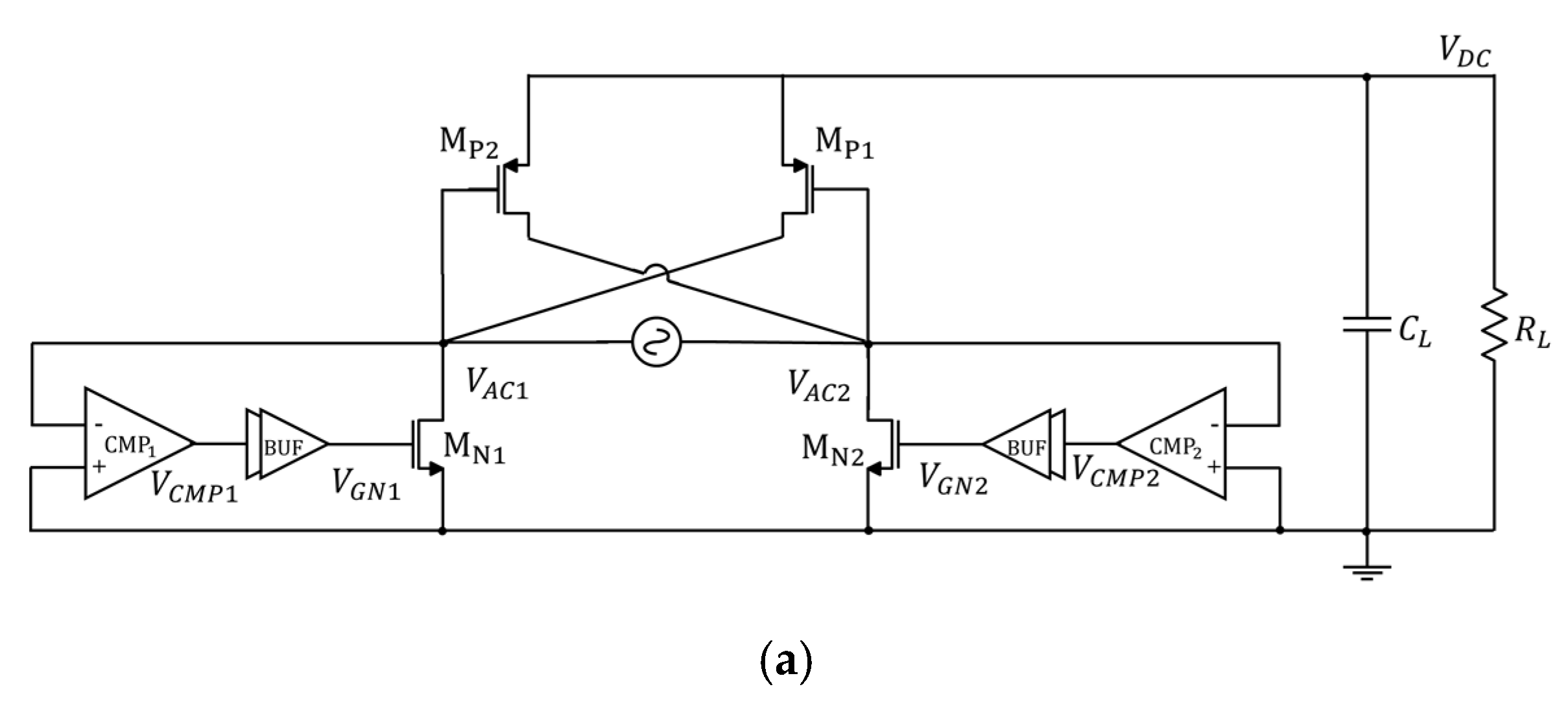
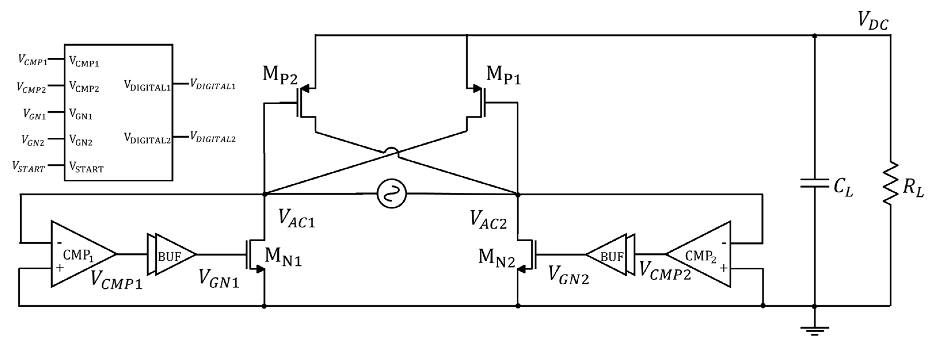
2. Introduction of Active Rectifier

The widely used full-wave active rectifier for the WPT system is displayed in Figure 2a, which consists of two cross-coupled PMOS and two comparator-controlled NMOS [2]. As for two cross-coupled PMOS MP1 and MP2, their gates are connected to VAC2 and VAC1, respectively, and their drains are connected to VAC1 and VAC2, respectively. However, the comparator and buffer have unavoidable propagation delays. Figure 2b illustrates a typical timing waveform when the active rectifier works. The propagation delay in the active rectifier mainly includes the comparator delay and the buffer delay. The turn-on delay will reduce the maximum transmittable power of the rectifier, and the turn-off delay will cause reverse current, which will greatly reduce the efficiency of the rectifier; therefore, both the turn-on delay and turn-off delay should be compensated for.
Common gate amplifier is widely used as the comparator in the rectifier, which also can be considered as a voltage-controlled current source. The comparator delay is the time that the comparator’s output current charges its output capacitor to half of the power supply, as illustrated in Figure 3. Detailed analysis can be found in [10]. The comparator delay can be expressed as follows:
t d , c = M C O U T T 2 π α g m = M C O U T T 2 π α 2 I B k n W / L 1 / I B 4 1 / V A C 4
where COUT is the load capacitance, T is the period of the AC input voltage, gm is the transconductance, IB is the bias current, α is a scaling factor, M is a factor equal to 0.9, and kn depends on the technology. In addition, V A C equals V A C 1 V A C 2 .
It can be seen from Equation (2) that the comparator delay is usually small since COUT is the input capacitance of the buffer, which is much smaller than the gate capacitance of the NMOS power transistor. Additionally, since the comparator delay is proportional to the fourth root of 1/|VAC|, it is less affected when the comparator’s supply voltage VDC changes; therefore, in this work, the comparator delay is considered to be equivalent to a fixed value, and it is directly subtracted during the delay compensation process.
As for the delay of the buffer, its delay can be analyzed by the cascading single-stage inverters. The propagation delay of a single inverter is [11]:
t p i n v 0.52 C L V D D W / L k V D S A T V D D V T V D S A T / 2
where VT is the threshold voltage, CL is the parasitic capacitance of the power transistor, VDD is the supply voltage, W and L are the width and length of NMOS in the inverter, respectively.
From Equation (3), it can be known that when the supply voltage changes, the propagation delay of the inverter will change accordingly.
The schematic diagram of the inverter chain is shown in Figure 4.
The expression of the minimum delay of the buffer (inverter chain) is [12]:
t p ,   m i n = N t p i n v 1 + F N / γ
where N is the stage number of the inverter, Cint is the intrinsic output capacitance of each inverter, Cg,i is the gate capacitance of the ith stage inverter, and γ = Cint/Cg,i, which is only related to the process and its value is approximately equal to 1 for most sub-micron process inverters. Assuming that each stage of the inverter has the same size enlargement factor f, the expression of F in Equation (4) is:
f N = F = C L C g , 1
In order to drive the power transistors with large gate capacitance well, a large-scale buffer is necessary to reduce the rising and falling delay of the power transistor, which can be known from Equations (4) and (5); however, the delay of the large-scale buffer is not negligible. Additionally, the delay of the buffer will greatly change with the power supply according to Equation (3); therefore, in this design, it is necessary to measure and eliminate the real-time delay of the buffer.
The power efficiency of the proposed rectifier can be denoted as follows:
η r e c = P O U T P I N
In Equation (6), P O U T is the output power which can be expressed as follows:
P O U T = V D C 2 R L
The power loss introduced by the reverse current is denoted as P R C , its calculation equation in a half period can be defined as follows:
P R C = V A C 1 , 2 2 R o n ,   n  
where R o n ,   n is the conduction resistance of NMOS power transistors M N 1 and M N 2 . This power loss is the elimination target in this work which has a great impact on the power conversion efficiency of the rectifier.

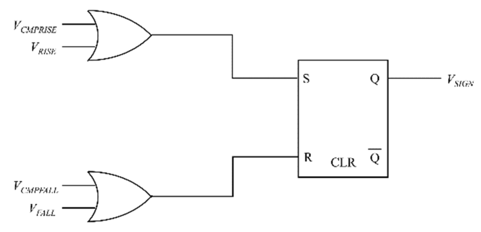
3. The Proposed Digitally Adaptive Delay Compensation Method

Figure 5 shows the structure of the active rectifier with the proposed compensation method. This paper proposes a two-step delay compensation method. Firstly, the turn-on and turn-off time of the rectifier, excluding the buffer’s delay and the compensation control circuit delay, is measured by the measurement module, then recorded by recording sequences, respectively. Secondly, a fixed value is initialized into recording sequences to eliminate the comparator delay. Both of the delay compensation steps are realized with digital circuits. As shown in Figure 5, the digital circuit is used to generate the compensation signal (VDIGITAL1 or VDIGITAL2). The compensation signal passes through the buffer to turn on or turn off the power transistor MN1 or MN2, respectively.
When the circuit environments changes, the rectified voltage VDC also changes; therefore, the delay-compensation control circuit should work continuously. Fortunately, the circuit environment usually changes slowly, so we choose to calibrate it every 1 μs, which is enough. The start signal (VSTART) is used, which is a 1 MHz square wave. At each rising edge of VSTART, the compensation control circuit will be triggered for calibration and perform a new round of compensation. In the following, we introduce the turn-on delay compensation and turn-off delay compensation, respectively, as well as the main implementation circuits.

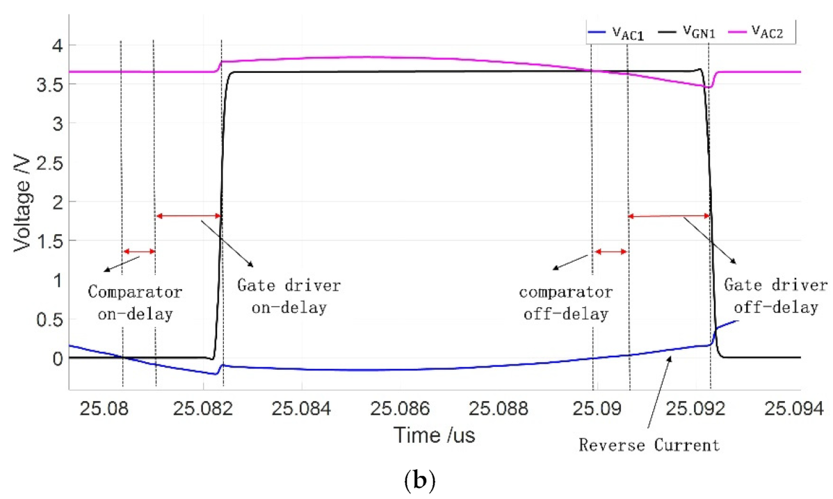
3.1. Turn-On Delay Compensation

As analyzed before, the delay of the buffer and the compensation control circuit is compensated in real-time. Besides that, the comparator delay is compensated by considering it as a constant. Let us consider the turn-on delay first.
When the rising edge of VSTART comes, the recording process of the digital module is triggered. As shown in Figure 6a, t1 is recorded by the recording sequence 1, which is the time from the falling edge of the buffer’s output to the rising edge of the comparator’s output. This time can be measured and recorded by using digital counters and registers with a 1 GHz reference clock.
According to the value recorded by recording sequence 1, the counting sequence generates the rising and falling edges of the compensation signal. Specifically, when the falling edge of the comparators’ output comes, the counting sequence starts counting until time passes by the recording value t1. At this time, the compensation control circuit generates the rising edge of the compensation signal VRISE in the next half period, as shown in Figure 6b. As the rising propagation delay is usually close to the falling propagation of the buffer and compensation control circuit, so the counting starts from the falling edge of the comparator’s output is reasonable. In addition, t3 is the comparator’s rising delay, t4 is the buffer’s rising delay, and t5 is the compensation control circuit’s rising delay, as illustrated in Figure 6b.
As analyzed before, t1 is the turn-on time of the rectifier, excluding the buffer’s delay t4 and digital module delay t5; however, there is still a comparator’s rising delay t3 that is not compensated. As for the comparator’s raising delay t3, it is considered as a constant. To realize the compensation of t3, a fixed value is initialized into recording sequence 1 directly in the second delay compensation stage to make MN1 and MN2 turn off in advance; therefore, the rising edge of the compensation signal VRISE is generated when the counting sequence passes through the time that is the recording time t1 minus the fixed comparator compensation time t3. For improving the robustness of the method, an adjustable 3-bit digital code is imported to the chip to make sure that the comparator delay is always well estimated for different process, voltage, and temperature cases.
In this way, the rising edge of the compensation signal VRISE eliminates the turn-on delay of the comparator, buffer, and compensation control circuit. Compared with VCMPRISE, which is the original comparator output, VRISE is earlier than VCMPRISE with (t3 + t4 + t5) as shown in Figure 6b. After the end of the recording process, the compensation control circuit no longer performs measurement and is only triggered until the next period rising edge of VSTART arrives.

3.2. Turn-Off Delay Compensation
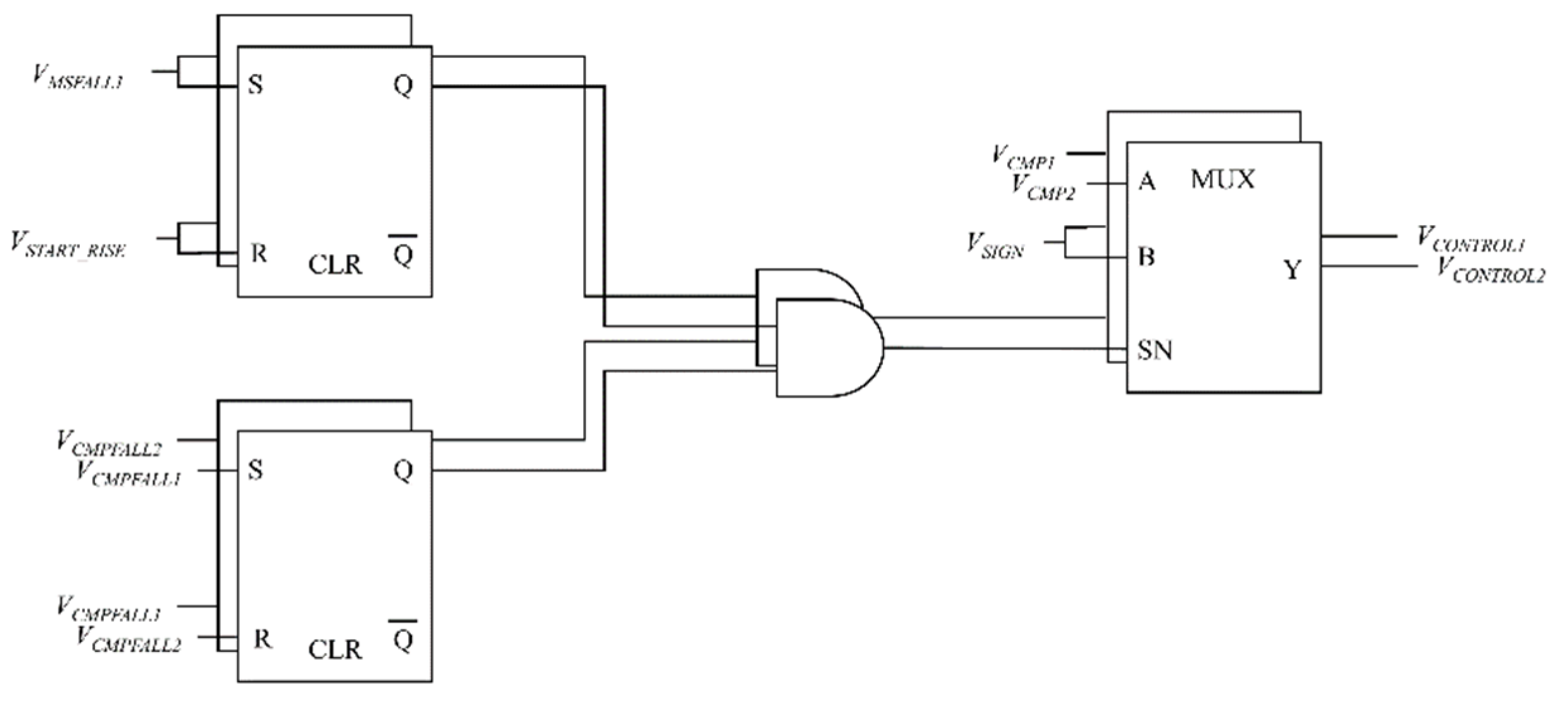
The turn-off delay compensation is similar to the turn-on delay compensation. As for the delay of the buffer and compensation control circuit, we propose to measure t2, which is the time from the rising edge of the buffer’s output to the falling edge of the comparator’s output, and then, t2 is recorded by the recording sequence 2. When the rising edge of the comparators’ output comes, the counting sequence starts counting until time passes by the value of the recording value t2 minus the fixed comparator compensation value t6. At this time, the digital module generates the falling edge of the compensation signal VFALL, as shown in Figure 6b. Compared with VCMPFALL, VFALL is earlier than VCMPFALL with (t6 + t7 + t8), in which the comparator’s turn-off delay t7 can be compensated with a method similar to that for the comparator’s turn-on delay cancelation.

4. Control Design

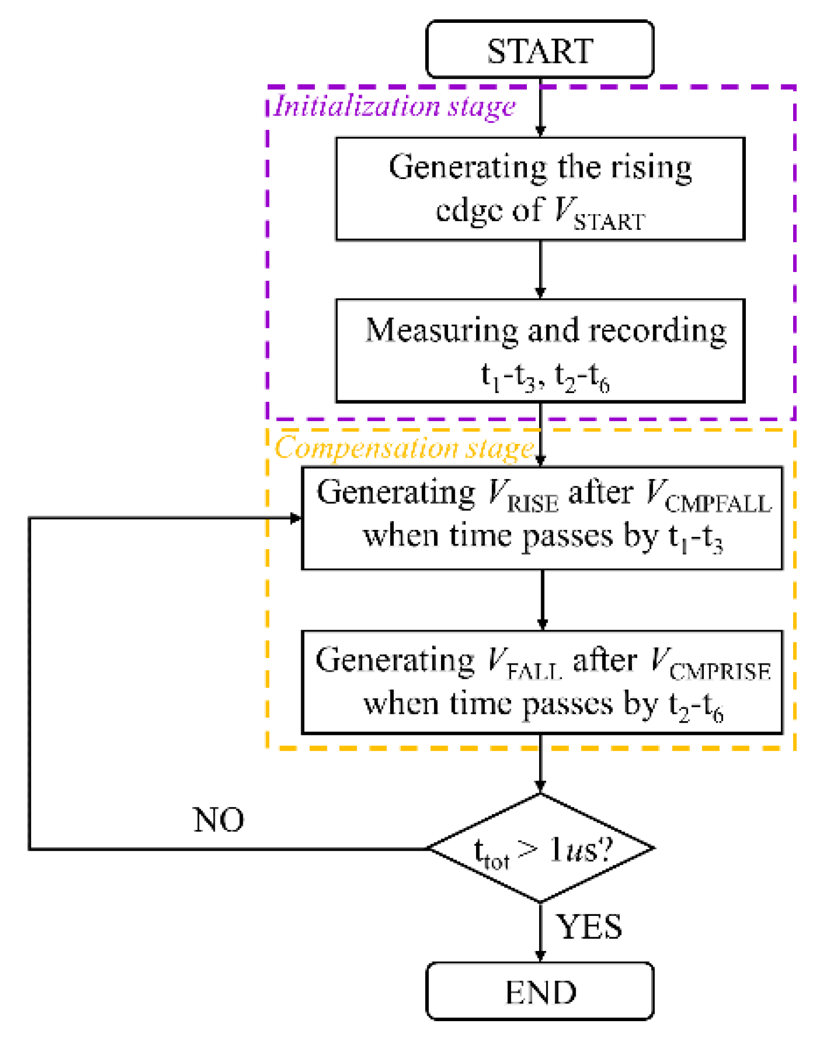
4.1. System Operation Process

As a summary of the proposed compensation method, the system process flowchart is illustrated in Figure 7 and is introduced as follows:
(1)
After starting the system, the rising edge of VSTART is generated, which activates the initialization stage of the system operation process.
(2)
t1 and t2 are measured and recorded in preparation for the generation of compensation signals.
(3)
After the falling edge of the comparator’s output, the rising edge of the compensation signal is generated when time passes through (t1t3).
(4)
After the rising edge of the comparator’s output, the falling edge of the compensation signal is generated when time passes through (t2t6). Until now, the compensation signal of only one NMOS has been generated.
(5)
The delay compensation control circuit continuously performs step (3) and step (4) until a new rising edge of VSTART is generated, and this processing cycle reaches the end. The rising edge of VSTART is generated every 1 μs to recalibrate the compensation control circuit, and it will not stop being generated unless the wireless power transfer system containing the proposed rectifier is turned off or the generation of the calibration signal VSTART is stopped.

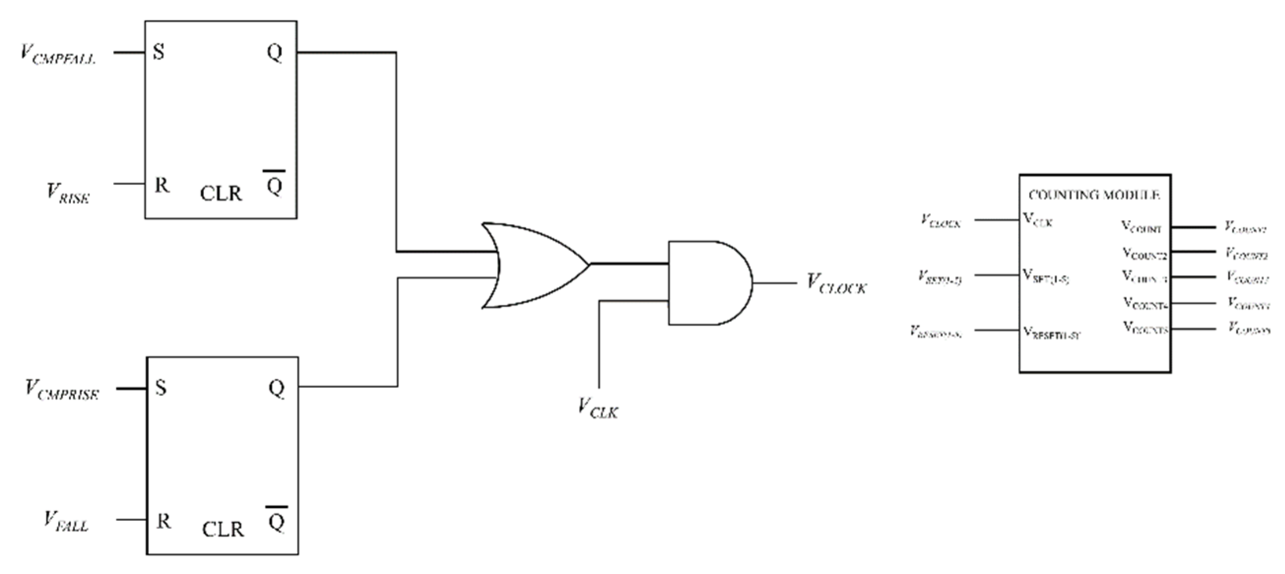
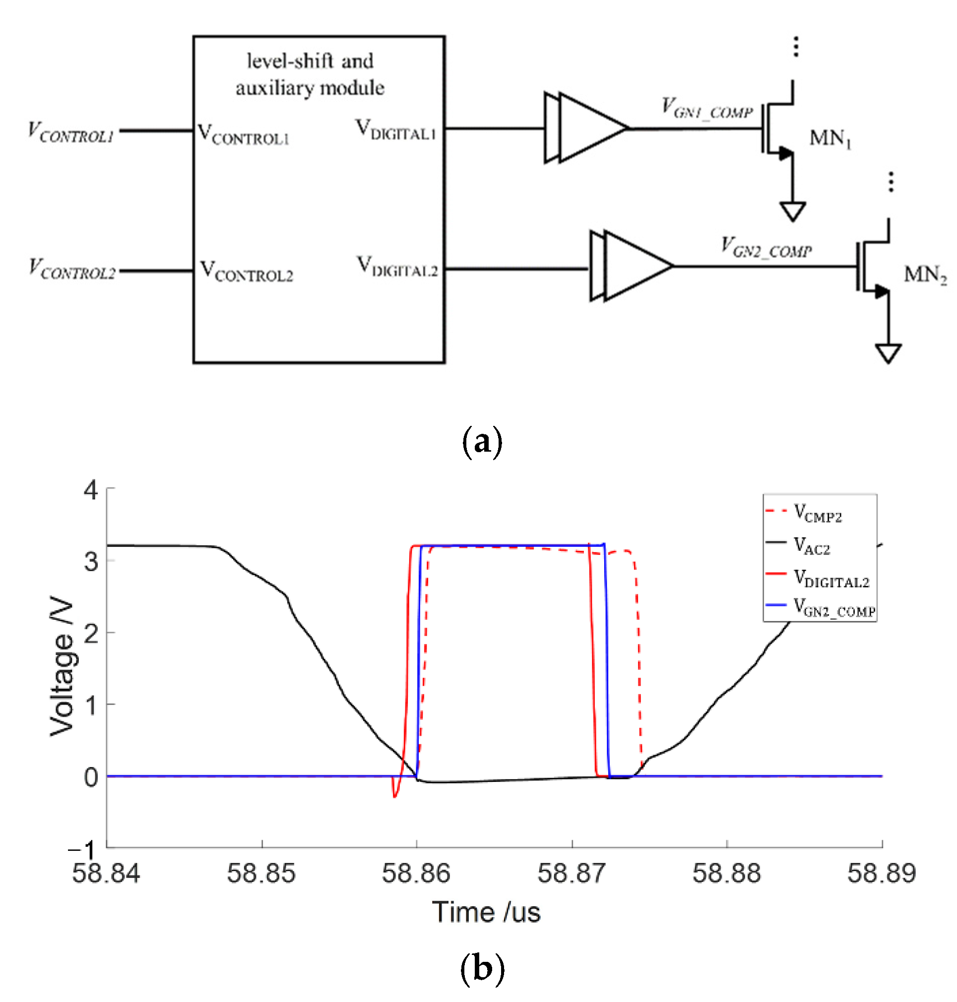
4.2. Circuit Implementation

In this section, the main implementation circuits are introduced in detail, including the recording sequence circuit, the counting sequence control circuit, and the compensation signals generating circuit.
As mentioned in Section 3, t1 and t2 are necessary to be measured for the next operation step. In the practical circuit, two auxiliary signals VMS1 and VMS2 are generated, as shown in Figure 8a. Taking a part of one period as an example, VMS1 remains high from the falling edge of VGN2 to the rising edge of VCMP1 and VMS2 remains high from the rising edge of VGN2 to the falling edge of VCMP2; therefore, t1 and t2 can be measured by measuring the high voltage duration of VMS1 and VMS2, respectively.
The recording sequence circuit consists of five flip-flops, as illustrated in Figure 8b. Take the recording sequence that records t1 as an example, it can only be activated when VMS1 is high. At the time of the new VSTART’s rising edge, the flip-flops are reset for recording the new measurement result.
In order to save the area and the cost of the counting control circuit, the counting task for generating either the rising or falling edge of the compensation signal is performed by one counting control circuit, as shown in Figure 9. This counting control circuit is activated to count at the comparator’s rising or falling edge until VCOUNT(1–5) are equal to VFRECORD(1–5) or VRRECORD(1–5), and VFRECORD(1–5) as well as VRRECORD(1–5) are the recording data of t1 and t2 in digital form, respectively. At the moment when the data are equal, the rising edge of compensation signal VRISE or the falling edge of compensation signal VFALL is generated by rear circuits and fed back into the counting control circuit, and thus the count is paused. As for the other two signals, VSET and VRESET, of the counting control circuit, they are used to set and reset the counting module’s initial value, which is used to eliminate the fixed comparator’s delay, respectively.
In the practical circuit, VRBIT(1–5) is the output of the comparison between VRRECORD(1–5) and VCOUNT(1–5), when VRRECORD(1–5) and VCOUNT(1–5) are equal in every five bits, the five bits of VRBIT are all high, and then VRSIE is generated. As for the process of VFALL’s generation, it is similar to the process of VRISE’s generation as introduced above.
For simplifying the control circuit, two channels that generate the compensation signals for MN1 and MN2 are combined in one circuit, as illustrated in Figure 10. This circuit is the only one signal path from the output of the comparator (CMP1 or CMP2) to the gate of NMOS; therefore, the NMOS will lose control once VRISE or VFALL is not generated successfully. For solving this potential problem and improving the robustness of the compensation control circuit, the rising edge signal and the falling edge signal of the comparator are also set as input signals of this circuit. When VRISE and VFALL are not generated, VCMPRISE and VCMPFALL replace them to control MN1 and MN2. Since the rising edge and the falling edge of compensation signal are earlier than VCMPRISE and VCMPFALL, the compensation signal VSIGN would not be disturbed by the change of VCMPRISE or VCMPFALL when VRISE and VFALL are generated normally.
As introduced in the system operation process, the compensation control circuit is recalibrated every 1 μs, then t1, t2 are remeasured and re-recorded at the initialization stage. At this stage, the comparator’s output is required to control MN1 and MN2 directly; therefore, a state-switching circuit is designed, as shown in Figure 11. At the beginning of the initialization stage, VSTART is generated and VCONTROL is selected to be equal to VCMP. At the end of the initialization stage, the recording process is terminated and VMS1 falls to the low level; then, VCONTROL is selected to be equal to VCMP. It should be noted that the state-switching circuit is also responsible for extracting VCONTROL1, VCONTROL2 from VSIGN to drive MN1 and MN2, respectively. Taking the state-switching circuit that controls MN2 as an example: at the time when the falling edge of VCMP1 is generated, VCONTROL2 is selected to be equal to VSIGN, and the generation of the falling edge of VCMP2 means that MN2 has been controlled to be turned on and off in its half period. In the next half period, VSIGN turns to control MN1 and VCONTROL2 is selected to be equal to VCMP2, which remains low in this half period.
Finally, VCONTROL1 and VCONTROL2 are processed by the level-shift and auxiliary module to generate the digital signals VDIGITAL1 and VDIGITAL2. After that, the compensated gate drive signals VGN1_COMP and VGN2_COMP are generated after the process of two-stage buffers to drive MN1 and MN2, respectively. This drive control circuit is illustrated in Figure 12a, and the waveforms of the main signals are displayed in Figure 12b. As for the auxiliary module, it is designed to solve the case that the compensation control circuit generates error compensation signals when the proposed rectifier is just started by locking the compensation signals to low.

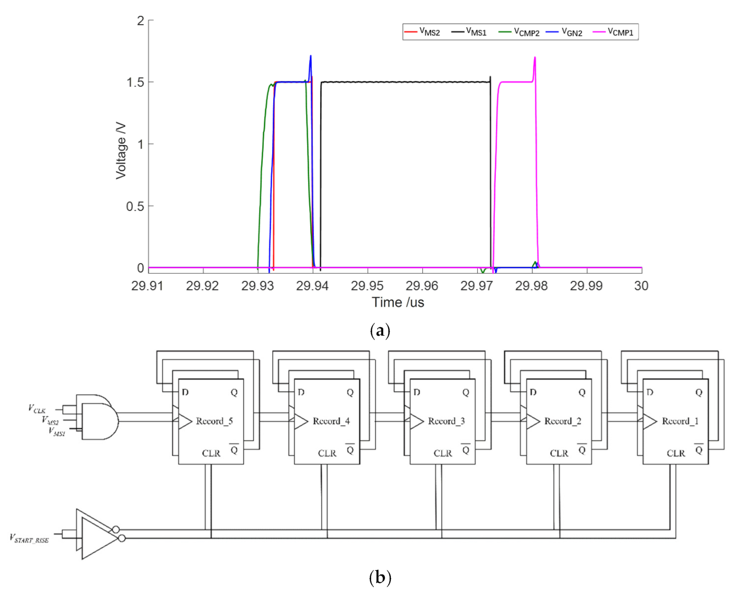
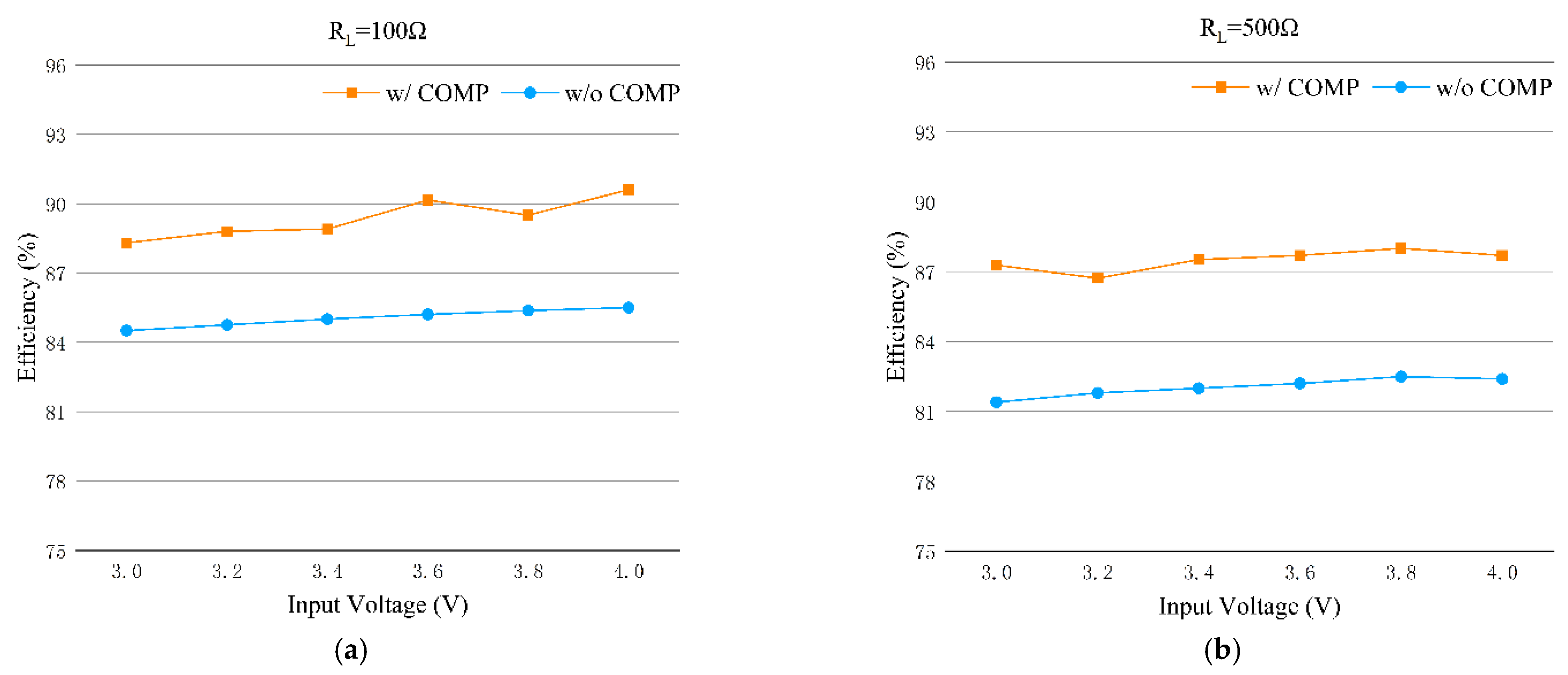
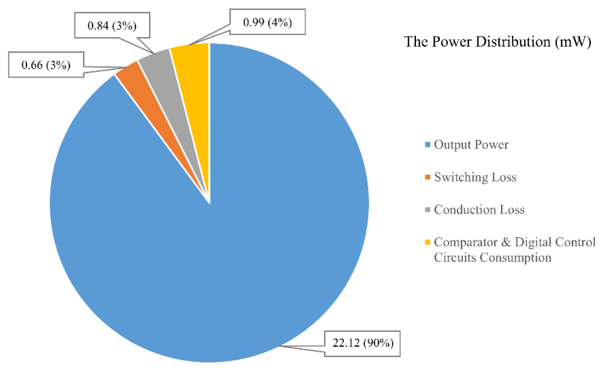
5. Simulation Results

The proposed rectifier was implemented and simulated in a standard 0.18 μm CMOS process whose parameters are listed in Table 1. Figure 13 shows the layout and the die photo of the proposed rectifier.
Figure 14 shows the main transient waveforms of the proposed rectifier. It shows that the compensated gate drive signal VGN1_COMP and VGN2_COMP turn off the rectifier earlier, and thus, the reverse current is eliminated. Additionally, it is satisfactory that the rectifier is not turned on too late due to the control of the compensation control circuit, which reduces the loss of the maximum transmittable power.
The power efficiencies of the proposed rectifier under different conditions that input voltage changes from 3 V to 4 V and the load resistance of 100 Ω or 500 Ω are displayed in Figure 15. As for the result, the rectifier’s efficiency is always higher than 86% and the highest power efficiency is 90.6% when the input is 4 V, and the load resistance is 500 Ω. We also designed and simulated a rectifier without the proposed compensation method; its power efficiency is also displayed in Figure 15. For the targeted input voltage and output load range, the highest efficiency is 85.5%, which is much lower than that of the proposed rectifier. Compared with the rectifier without the compensation method, the efficiency of the proposed rectifier is increased by up to 7%.
For more details, the power distribution of the proposed active rectifier is shown in Figure 16. It can be seen that the compensation control circuit of the proposed rectifier only consumes little power, and the rectifier can achieve an efficiency as high as 90%.
As shown in Table 2, the performance of the proposed rectifier is concluded and compared with the state-of-the-art designs. The peak efficiency is almost 91% at the load of 500 Ω and the input voltage of 4 V, respectively. In this work, the value of turn-on and turn-off compensation delay are 2 ns and 2.5 ns, respectively. These values are competitive in the works which are published in recent years. For example, in [13], the value of turn-on and turn-off compensation delay are 0.75~1.5 ns and −0.7~0.5 ns, respectively. In [14,15], these values are both about 4 ns and 2~4 ns, respectively.
As for the complexity, the proposed fully digital delay compensation circuit is built by a small number of simple logic gates and basic flip-flops composed of active devices. In addition, the proposed delay compensation circuit is shared by MN1 and MN2 compensation control method, instead of using two identical circuits to compensate MN1 and MN2, respectively; however, the proposed delay compensation circuits are all mixed-signal circuits in [15,16]. Especially in [16], there are some passive devices that exist in the proposed delay compensation circuit. In [9], two identical circuits are used to compensate MN1 and MN2, respectively, which also increases the circuit complexity.
In order to evaluate the impact of the output load change on power conversion efficiency, a figure of merit (FoM) is introduced and listed in Table 2. It is defined as follows:
F o M = η 100 Ω η 500 Ω η 500 Ω
where η 100 Ω and η 500 Ω are the power conversion efficiency at the load of 100 Ω and 500 Ω, respectively. A smaller FoM value means that the power conversion efficiency is less affected by the variation of the load, and the proposed rectifier’s FoM value is comparable to previous state-of-the-art work.

6. Conclusions

An efficiency-improving CMOS active rectifier with the digitally on-delay and off-delay compensation control circuit is developed in this paper. The compensation control circuit adaptively regenerates the compensated gate drive signal to control the NMOS to turn on and off in advance by measuring and recording the NMOS’s turn-on delay and turn-off delay, and thus, the reverse current is eliminated, and the efficiency of the rectifier is improved. The simulation results show that this work is indeed effective in eliminating the delay of NMOS and is competitive compared with the previous state-of-the-art design.

Author Contributions

The authors contributed to different parts of the paper preparation as follows: Conceptualization, J.M. and X.T.; methodology and software, J.M. and X.T.; validation and analysis, Y.Z.; writing—original draft preparation, Y.Z. and X.T.; writing—review and editing, Y.Z. and X.T.; supervision, X.T. All authors have read and agreed to the published version of the manuscript.

Funding

This work was funded by Shenzhen Basic Research Foundation (No. JCYJ20180508152019687 and WDZC20200819152116001).

Institutional Review Board Statement

Not applicable.

Informed Consent Statement

Not applicable.

Data Availability Statement

Not applicable.

Conflicts of Interest

The authors declare no conflict of interest.

References

  1. Junye, M.; Xian, T.; Wai Tung, N.; Mingming, Z. A High-Efficiency Active Rectifier with Adaptive Off-Delay Compensation for Wireless Power Transfer Systems. In Proceedings of the 2020 IEEE 5th International Conference on Integrated Circuits and Microsystems (ICICM), Nanjing, China, 23–25 October 2020; pp. 1–4. [Google Scholar]
  2. Lam, Y.H.; Ki, W.H.; Tsui, C.Y. Integrated low-loss CMOS active rectifier for wirelessly powered devices. IEEE Trans. Circuits Syst. II—Express Briefs 2006, 53, 1378–1382. [Google Scholar] [CrossRef]
  3. Guo, S.; Lee, H. An Efficiency-Enhanced CMOS Rectifier with Unbalanced-Biased Comparators for Transcutaneous-Powered High-Current Implants. IEEE J. Solid-State Circuits 2009, 44, 1796–1804. [Google Scholar] [CrossRef]
  4. Cha, H.K.; Park, W.T.; Je, M. A CMOS Rectifier with a Cross-Coupled Latched Comparator for Wireless Power Transfer in Biomedical Applications. IEEE Trans. Circuits Syst. II—Express Briefs 2012, 59, 409–413. [Google Scholar] [CrossRef]
  5. Cheng, L.; Ki, W.H.; Lu, Y.; Yim, T.S. Adaptive On/Off Delay-Compensated Active Rectifiers for Wireless Power Transfer Systems. IEEE J. Solid-State Circuits 2016, 51, 712–723. [Google Scholar]
  6. Kao, S.K. A CMOS Active Rectifier with Time Domain Technique to Enhance PCE. Electronics 2021, 10, 13. [Google Scholar] [CrossRef]
  7. Banerjee, A.; Bhattacharyya, T.K.; Nag, S. High efficiency CMOS active rectifier with adaptive delay compensation. Microelectron. J. 2021, 112, 105052. [Google Scholar] [CrossRef]
  8. Tong, X.; Li, M. A High-Efficiency Receiving Circuit for Wireless Power Transmission. In Proceedings of the 2019 14th IEEE Conference on Industrial Electronics and Applications (ICIEA), Xi’an, China, 19–21 June 2019; pp. 1185–1188. [Google Scholar]
  9. Luo, Z.; Lee, H. A 40.68MHz Active Rectifier with Cycle-Based On/Off-Delay Compensation for Biomedical Implants. In Proceedings of the ESSCIRC 2021—IEEE 47th European Solid State Circuits Conference (ESSCIRC), Grenoble, France, 13–22 September 2021; pp. 227–230. [Google Scholar]
  10. Lu, Y.; Ki, W.H. A 13.56 MHz CMOS Active Rectifier with Switched-Offset and Compensated Biasing for Biomedical Wireless Power Transfer Systems. IEEE Trans. Biomed. Circuits Syst. 2014, 8, 334–344. [Google Scholar] [CrossRef] [PubMed]
  11. Lu, Y.; Ki, W. CMOS Integrated Circuit Design for Wireless Power Transfer; Springer: Berlin/Heidelberg, Germany, 2018. [Google Scholar]
  12. Rabaey, J.M.; Chandrakasan, A.; Nikolic, B. Digital Integrated Circuits: A Design Perspective, 2nd ed.; Prentice-Hall: Hoboken, NJ, USA, 2003. [Google Scholar]
  13. Lee, H.M.; Ghovanloo, M. An Integrated Power-Efficient Active Rectifier with Offset-Controlled High Speed Comparators for Inductively Powered Applications. IEEE Trans. Circuits Syst. I—Regul. Pap. 2011, 58, 1749–1760. [Google Scholar] [CrossRef] [PubMed] [Green Version]
  14. Huang, C.; Kawajiri, T.; Ishikuro, H. A Near-Optimum 13.56 MHz CMOS Active Rectifier with Circuit-Delay Real-Time Calibrations for High-Current Biomedical Implants. IEEE J. Solid-State Circuits 2016, 51, 1797–1809. [Google Scholar] [CrossRef]
  15. Xue, Z.M.; Fan, S.Q.; Li, D.; Zhang, L.N.; Gou, W.; Geng, L. A 13.56 MHz, 94.1% Peak Efficiency CMOS Active Rectifier with Adaptive Delay Time Control for Wireless Power Transmission Systems. IEEE J. Solid-State Circuits 2019, 54, 1744–1754. [Google Scholar] [CrossRef]
  16. Noh, K.; Amanor-Boadu, J.; Zhang, M.L.; Sanchez-Sinencio, E. A 13.56-MHz CMOS Active Rectifier with a Voltage Mode Switched-Offset Comparator for Implantable Medical Devices. IEEE Trans. Very Large Scale Integr. (VLSI) Syst. 2018, 26, 2050–2060. [Google Scholar] [CrossRef]
  17. Wu, C.Y.; Qian, X.H.; Cheng, M.S.; Liang, Y.A.; Chen, W.M. A 13.56 MHz 40 mW CMOS High-Efficiency Inductive Link Power Supply Utilizing On-Chip Delay-Compensated Voltage Doubler Rectifier and Multiple LDOs for Implantable Medical Devices. IEEE J. Solid-State Circuits 2014, 49, 2397–2407. [Google Scholar] [CrossRef]
  18. Erfani, R.; Marefat, F.; Nag, S.; Mohseni, P. A 1–10-MHz Frequency-Aware CMOS Active Rectifier with Dual-Loop Adaptive Delay Compensation and >230-mW Output Power for Capacitively Powered Biomedical Implants. IEEE J. Solid-State Circuits 2020, 55, 756–766. [Google Scholar] [CrossRef]
  19. Oh, S.J.; Khan, D.; Jang, B.G.; Basim, M.; Asif, M.; Ali, I.; Pu, Y.; Yoo, S.S.; Lee, M.; Hwang, K.C.; et al. A 15-W Quadruple-Mode Reconfigurable Bidirectional Wireless Power Transceiver with 95% System Efficiency for Wireless Charging Applications. IEEE Trans. Power Electron. 2021, 36, 3814–3827. [Google Scholar] [CrossRef]
  20. Namgoong, G.; Choi, E.; Park, W.; Lee, B.; Park, H.; Ma, H.; Bien, F. 3–12-V Wide Input Range Adaptive Delay Compensated Active Rectifier for 6.78-MHz Loosely Coupled Wireless Power Transfer System. IEEE Trans. Circuits Syst. I Regul. Pap. 2021, 68, 2702–2713. [Google Scholar] [CrossRef]
Figure 1. Typical structure of wireless power transfer system for biomedical implants.
Energies 14 08089 g001
Figure 2. (a) The schematic and (b) the waveforms with various delays of the widely used active rectifier.
Energies 14 08089 g002aEnergies 14 08089 g002b
Figure 3. The schematic diagram of comparator delay analysis.
Energies 14 08089 g003
Figure 4. The schematic diagram of the buffer chain.
Energies 14 08089 g004
Figure 5. The implementation of the proposed active rectifier.
Energies 14 08089 g005
Figure 6. The waveforms of (a) rectifier working status and (b) various delays.
Energies 14 08089 g006
Figure 7. The flowchart of the proposed compensation method in one cycle.
Energies 14 08089 g007
Figure 8. (a) The waveforms of the auxiliary signals and (b) the schematic diagram of the recording sequence circuit.
Energies 14 08089 g008
Figure 9. The schematic diagram of the counting control circuit.
Energies 14 08089 g009
Figure 10. The schematic diagram of the compensation signal VSIGN generation circuit.
Energies 14 08089 g010
Figure 11. The schematic of the state-switching circuit.
Energies 14 08089 g011
Figure 12. (a) The schematic of the drive control circuit and (b) the waveforms of main signals.
Energies 14 08089 g012
Figure 13. (a) The layout and (b) the die photo of the proposed rectifier.
Energies 14 08089 g013
Figure 14. The main experimental transient waveform of the proposed rectifier.
Energies 14 08089 g014
Figure 15. The power efficiency of the proposed rectifier and the rectifier without compensation method with (a) 100 Ω and (b) 500 Ω load resistance.
Energies 14 08089 g015
Figure 16. The pie graph of the power distribution.
Energies 14 08089 g016
Table 1. System parameters.
ParametersValue
System Operation Frequency13.56 MHz
Input Voltage3~4 V
Load of Resistance100~500 Ω
Table 2. Comparisons with previous active rectifiers.
PapersApplicationTechnologyFrequencyInput RangeType of MOSFETDelay CompensationPower Conversion EfficiencyFoMPOUT,max
TCAS-I’11 [13]Biomedical
WPT
System
0.5 μm13.56 MHz2.5–3.9 VPMOSOn & Off68–80.2% (@500 Ω)0.11120 mW
TBCAS’14 [10]0.18 μm13.56 MHz1.5–4 VNMOSOff82.2–90.1% (@500 Ω)0.06024.8 mW
JSSC’14 [17]65 nm13.56 MHz1.15–1.35 VNMOS & PMOSOn & Off72.5–85% (@500 Ω)N/A40 mW
JSSC’16 [14]65 nm13.56 MHz1.3–2.5 VNMOSOn & Off88.5–91.0% (@500 Ω)
91.3–94.6% (@100 Ω)
0.057248.1 mW
VLSI’18 [16]0.35 μm13.56 MHz2.9–5.4 VNMOSOn & Off84.6–86.1% (@500 Ω)
85.8–89.0% (@200 Ω)
N/A12.67 mW
JSSC’19 [15]0.18 μm13.56 MHz1.0–2.5 VNMOSOn & Off82.6–92.9% (@1000 Ω)
85.0–94.1% (@510 Ω)
N/A34.1 mW
JSSC’20 [18]0.18 μm1–10 MHz1.8–5 VPMOSOn & Off84.4–91.5% (@300 Ω)
85.2–91.8% (@100 Ω)
0.022231.6 mW
MDPI Elec.’21 [6]0.18 μm13.56 MHz1.8–3.6 VNMOSOn & Off83.0–90.3%
(@100 Ω–1.3 kΩ)
0.011109 mW
ESSCIRC’21 [9]0.18 μm40.68 MHz1.9–3.8 VNMOSOn & Off81.6–85.1% (@200 Ω)
81.9–86.0% (@100 Ω)
N/A207 mW
TPE’21 [19]0.18 μm85–500 kHz/6.78 MHzN/ANMOSOn & Off96.2% (@150 kHz)
93.6% (@6.78 MHz)
N/A15 W
TCAS-I’21 [20]0.18 μm6.78 MHz3–10 VNMOSOn & Off82.0–93.6% (@1 kΩ)
86.0–93.7% (@500 Ω)
N/A288 mW
This Work’210.18 μm13.56 MHz3–4 VNMOSOn & Off87.2–88% * (@500 Ω)
88.3–90.6% * (@100 Ω)
0.02922.12 mW
* Simulation Result.
Publisher’s Note: MDPI stays neutral with regard to jurisdictional claims in published maps and institutional affiliations.

