2.1. Proposed Piecewise Modeling of Output-Voltage Ripple for 1-Stage Linear Charge Pump
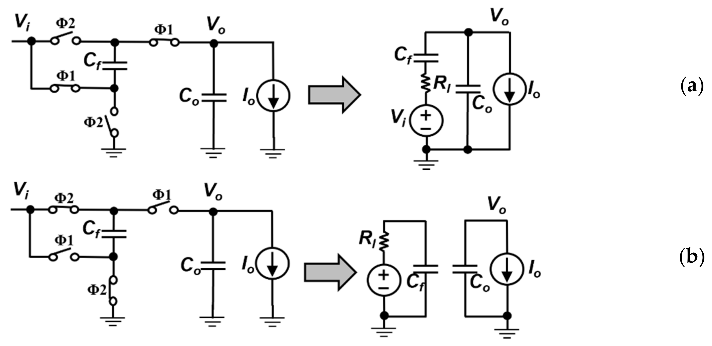
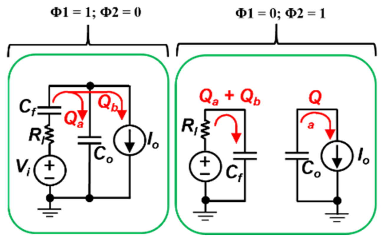
The two-phase switching operation of a 1-stage linear charge pump is shown in
Figure 1. Two complementary clock signals Φ1 and Φ2, which have approximately half of a switching period (
T), are used to control the ON and OFF of switches. Deadtime is inserted in transitions between Φ1 and Φ2 to avoid short-circuit loss of the switches.
Vi, Vo and
Io represent input voltage, output voltage and output current.
Cf and
Co are flying and output capacitors. Assuming the lump resistances of switches are the same, the lump sum of the resistances from switches, routing and bond-wire could be noted as
Rl, which is around two times of a single switch.
Figure 1a shows the case for Φ1 = 1 and Φ2 = 0.
Vi and
Cf are connected in series to generate approximately two times of
Vi for
Vo. The corresponding modeling is shown on the right-hand side of
Figure 1a. Similarly,
Figure 1b shows the case for Φ1 = 0 and Φ2 = 1.
Cf is charged by
Vi, while
Co maintains
Vo and supply current to load. The right-hand-side figure of
Figure 1b shows the modeling. When
T/2 is larger than about 6
RlCf, the voltage across
Cf is close to
Vi. However, usually
Cf could not be fully charged since a large
T leads to large output voltage drop due to the long discharging time of
Co.
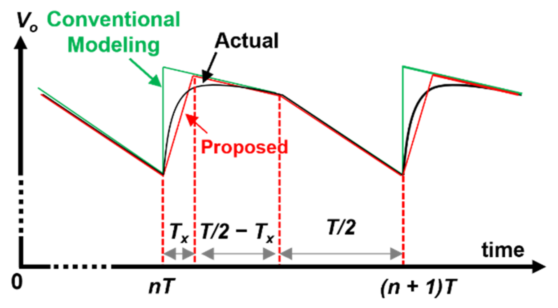
Figure 2 shows the output-voltage ripples of a 1-stage linear charge pump. The actual output-voltage ripple is represented by the solid black line. The green line shows the modeling proposed in [
7]. There is no charging time of
Cf and no charge re-distribution between
Cf and
Co in this modeling so that
Vo is sharply increased at
nT in the
n-th switching cycle. Since the average
Vo (i.e.,
) is used to evaluate PCE in [
7], inaccurate modeling of the output-voltage ripples results in inaccurate
and PCE.
The proposed modeling of the output-voltage ripples is shown by the red line in
Figure 2. There are three segments within a switching period, and each segment is represented by a straight line. A short period of
Tx is used to model the situation when
Vo raises at
nT. Comparing the proposed modeling with the actual output-voltage ripple shows that the proposed piecewise method can better represent the ripple voltage at output. Thus,
and PCE can be predicted more accurately.
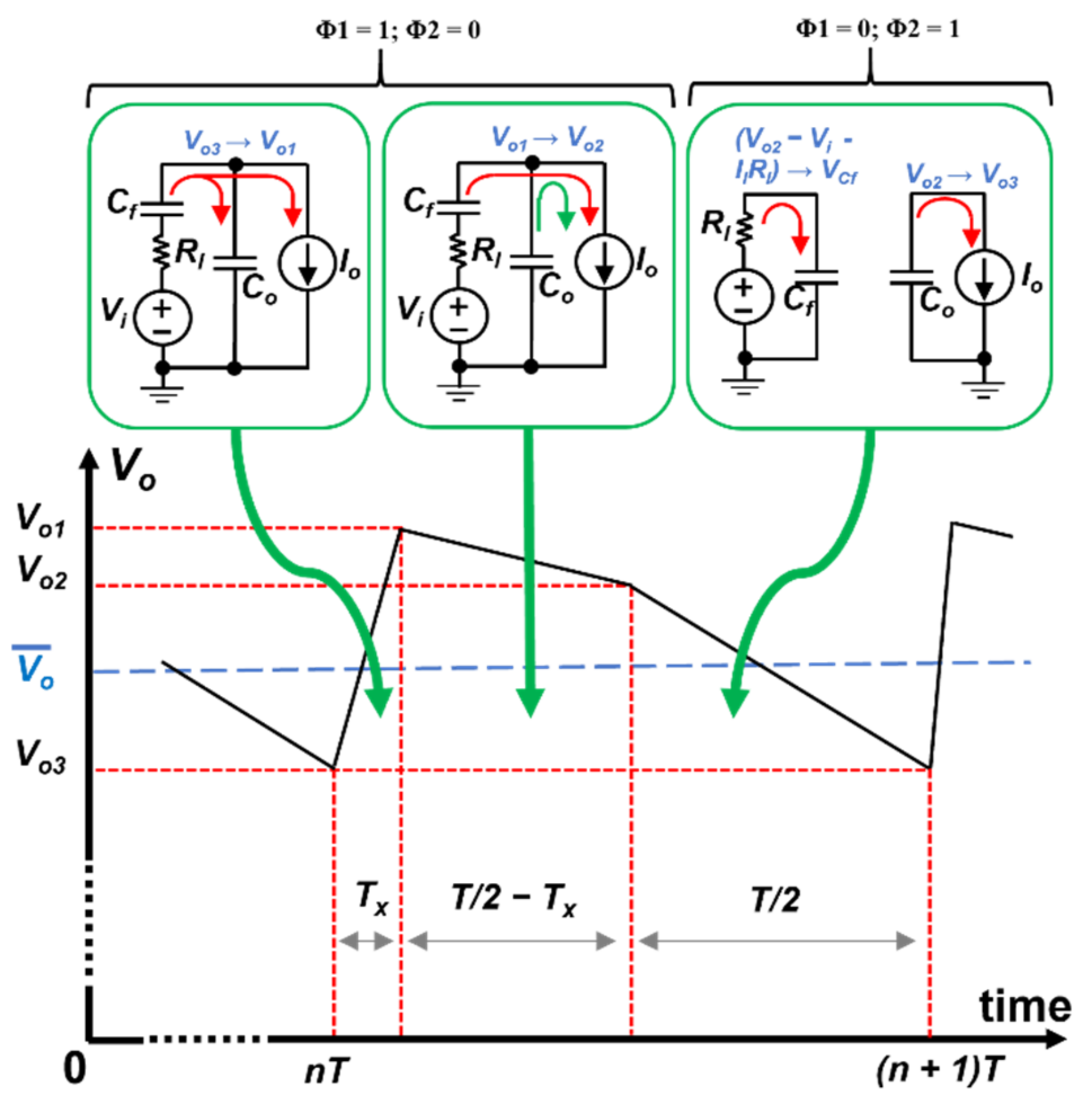
Figure 3 shows more details of the output waveform and the corresponding RC circuits (from
Figure 1) of a 1-stage linear charge pump.
Vo starts at
Vo3 at
nT and reaches
Vo1 within
Tx. Then, it decreases from
Vo1 to
Vo2 within (
T/2 −
Tx). Finally, it further decreases from
Vo2 to
Vo3 to complete a cycle. More details will be provided below to investigate the up and down of
Vo within a switching cycle to generate the voltage ripple.
In the previous cycle, Cf is previously charged to VCf, which is close to Vi, while Co is lightly discharged by the load and the voltage across Co is less than 2Vi. At nT, the series-connected combination of the voltage source Vi and Cf has a sum of voltage of Vi + VCf. Thus, Cf is discharged itself to provide charges to Co and the load Io. As the voltage across Co is increasing, Vo is increased from Vo3 to Vo1, and the required time to complete this operation is Tx.
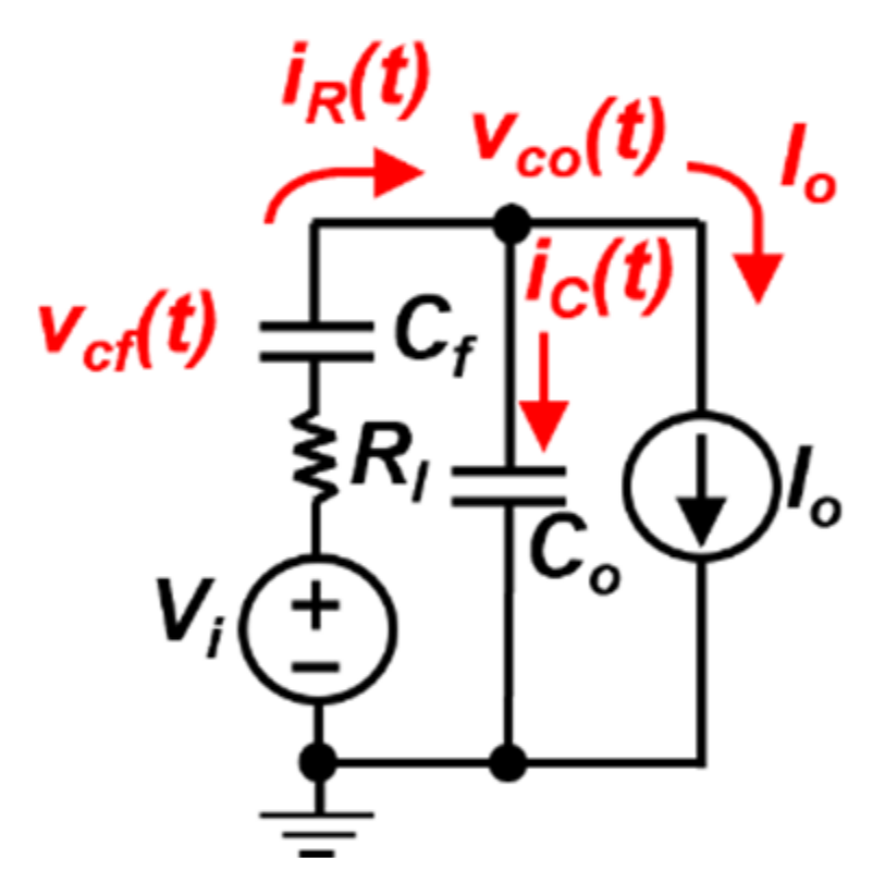
From the
RC circuits in
Figure 3, at
nT, the voltage of
Cf is
VCf, and thus the charge of
Cf is
CfVCf. Moreover, the charge of
Co is
CoVo3. Then, at (
nT +
Tx), the voltage across
Cf is dropped to (
Vo1 −
Vi −
IlRl), so that the charges of
Cf is
Cf (Vo1 −
Vi −
IlRl).
IR1 has the same value as
Io, since the current going into
Co should be zero at (
nT +
Tx). Meanwhile, the charge of
Co is
CoVo1. The charge supplied to the load is
IoTx. By principle of conservation of charges [
7], the following relationship is achieved.
VCf is the voltage obtained by capacitor
Cf when charging with an ideal voltage supply
Vi within a time period
T/2, and the initial voltage is
Vo2. Therefore,
VCf is given by
At (
nT +
T/2), the voltage of
Co is
Vo2. Since the charge redistribution of
Cf and
Co is complete, the current passing through
Cf and
Co is in constant ratio. Therefore, the current of
Cf should be
CfIo/(
Cf + Co). As a result, the following relationship is obtained.
Between (
nT +
T/2) and (
n + 1)
T, the voltage across
Co drops from
Vo2 to
Vo3. The change of charges of
Co is
Co (
Vo2 −
Vo3). These charges supply current to the load to give
Assume that
,
, and
. It should be noted that
, i.e.,
, so that the charge redistribution between
Cf and
Co is complete. By solving Equations (1)–(4),
Vo1,
Vo2 and
Vo3 can be found, respectively.
From Equations (5)–(7), as well as the durations of each segment within a switching cycle, the average value of
Vo is found and given by:
For
m3 in Equation (8), it can be evaluated by the following. Refer to
Figure 4 for the currents and voltages of
Cf and
Co during the period from
nT to (
nT +
Tx), it can be found that
By considering the charges in capacitors and differentiating in Equation (9) on both sides with respect to time, it gives
where
Qcf(
t) and
Qco(
t) are the charges stored in
Cf and
Co at
t. From
Figure 4, it can be found that
and
. Based on these relationships and substituting into Equation (9), the following expression is obtained. It is noted that
as
Vi is a dc voltage.
Solving the above differential equation, and determining the constant of integration by the initial condition of the circuit, the expression of
iR(
t) is given by
where
. The capacitor current of
Co is given by
where
is the initial current of
Co at
nT.
Refering to
Figure 2, the peak voltage of
Vo (i.e., the peak voltage across
Co) occurs at about (
nT +
Tx). Therefore,
Tx can be found by differentiating Equation (11) with respect to time to find the maximum point. As a result,
Tx is given by
By solving Equation (14), we have
Figure 5 shows the charge transfer in both phases. In Phase 2, the total charges from
Co to load is
Qa, and so
. Since the output-voltage waveform is periodic, the net charges leaving
Co in Phase 2 equals to the net charges inputted into
Co in Phase 1. Thus, the injected charges to
Co in Phase 1 is also
Qa. Assuming the net charges to load in Phase 1 is
Qb where
, the charges from
Cf in Phase 1 becomes (
Qa +
Qb). For the series connections of
Vi and
Cf in Phase 1, the charges from
Vi is also (
Qa +
Qb) in Phase 1. Since, again, the output-voltage waveform is periodic, the net charges leaving
Cf in Phase 1 equals to the net charges inputted into
Cf in Phase 2. As such, the charges from
Vi to
Cf in Phase 2 is (
Qa +
Qb). The total charges from
Vi is equal to (
Qa +
Qb) in Phase 1 plus (
Qa +
Qb) in Phase 2, which is
2(Qa +
Qb) =
2IoT. Therefore, the input current (
Ii) from
Vi is given by two times of
Io (i.e.,
Ii = 2
Io), which is two times the load current.
The PCE of a 1-stage linear charge pump is the ratio of output power (
Po) to input power (
Pi) and is given by
where
is the expression shown in Equation (8).
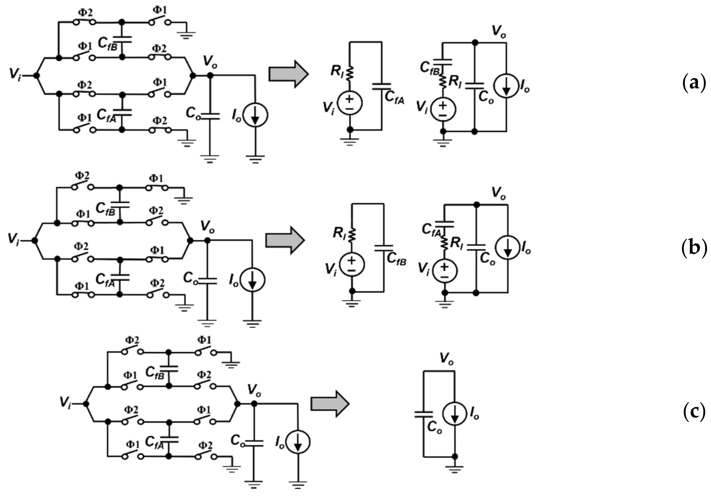
2.2. Proposed Piecewise Modeling of Output-Voltage Ripple for Dual-Branch 1-Stage Linear Charge Pump/Cross-Coupled Voltage Doubler
In this section, the proposed piecewise modeling of output-voltage ripple is applied to dual-branch 1-stage linear charge pump. It is applicable to cross-coupled voltage doubler, since the ON and OFF arrangements of switches of both dual-branch 1-stage linear charge pump and cross-coupled voltage doubler are the same.
Figure 6 shows the switching of a dual-branch 1-stage linear charge pump or cross-coupled voltage doubler, where
CfA and
CfB are flying capacitors. Similarly,
Rl is used to denote the lump sum of the resistances from switches, routing, and bond-wire. The parallel structure enables the load supplied by the flying and output capacitors simultaneously when Φ1 = 1; Φ2 = 0 and Φ1 = 0; Φ2 = 1, except that only
Co provides charges to the load at deadtime (i.e., Φ1 = 0; Φ2 = 0). In fact,
Td is much shorter than
T.
Figure 6a shows the case for Φ1 = 1 and Φ2 = 0.
Vi and
CfA are connected in series to generate approximately two times of
Vi for
Vo, and
CfB is charged by
Vi. The corresponding modeling is shown on the right-hand side of
Figure 6a.
Rl, same as before, is the lump sum of the resistances from switches, routing, and bond-wire. Similarly,
Figure 6b shows the case for Φ1 = 0 and Φ2 = 1.
Vi and
CfB are connected in series to provide about two times of
Vi for
Vo, and
CfA is charged by
Vi. The right-hand-side figure of
Figure 6b shows the modeling. Finally,
Figure 6c shows the moment of deadtime (i.e., the case for Φ1 = 0 and Φ2 = 0), where all switches are turned off. Only
Co maintains about 2
Vi and supplies charges to the load.
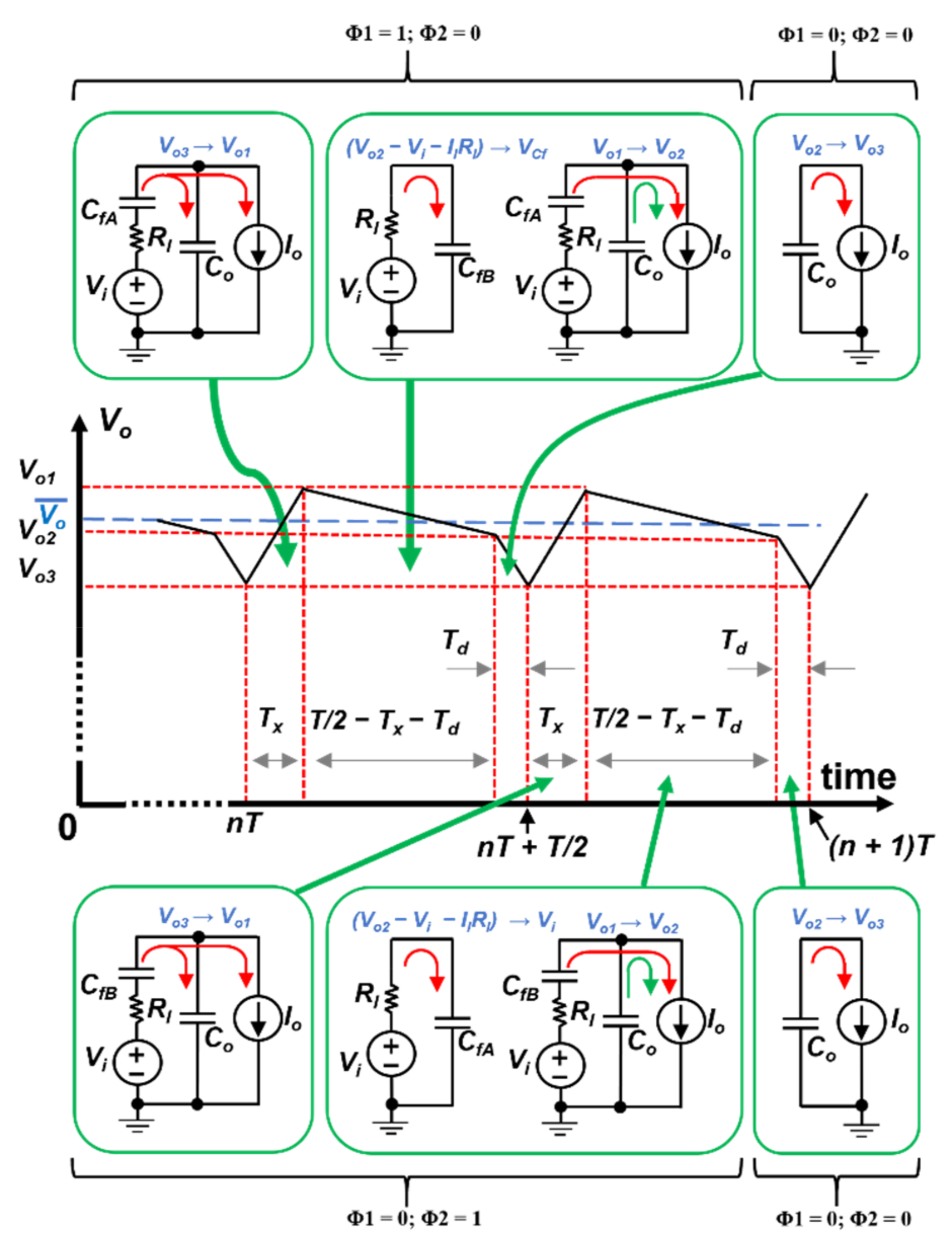
Figure 7 shows more details of the output waveform of one switching cycle and the corresponding
RC circuits (from
Figure 6) of a dual-branch 1-stage linear charge pump and cross-coupled voltage doubler. In the previous cycle,
CfA is previously charged to
VCf, which is close to
Vi, while
Co is lightly discharged by the load and the voltage across
Co is less than 2
Vi. At
nT, the series-connected combination of the voltage source
Vi and
CfA has a sum of voltage of
Vi +
VCf. Thus,
CfA is discharged itself to provide charges to
Co and the load.
CfB is connected with
Vi for re-charging. As the voltage across
Co is increasing,
Vo is increased from
Vo3 to
Vo1, and the required time to complete this operation is
Tx. After
Tx, where the output voltage achieves the highest value, both
CfA and
Co discharge themselves to provide charges to the load. The duration is (
T/2 −
Tx −
Td), and
Vo drops to
Vo2 finally. At (
nT +
T/2 −
Td), all switches are turned off in the deadtime period. Only
Co supplies charges to the load. Thus, the drop of
Vo is more rapid than before. At (
nT +
T/2),
Vo reaches
Vo3 to complete half of a cycle. Between (
nT +
T/2) and (
n + 1
)T, the operation of the first half switching cycle repeats. The only difference is that another half of the circuit enables
CfB to supply charges to the load. In the above analysis, it is assumed that
T/2 is longer than 6
Rl(Cf//
Co) (where
Cf =
CfA =
CfB) to ensure that the redistribution of
Cf (
CfA and
CfB) and
Co is complete when the capacitors are connected.
As shown in
Figure 7, the output-voltage waveforms in the first half and second half of a switching cycle are the same. The analysis below takes a period of
T/2 into account.
CfA and
CfB are considered to have the same value, such that
CfA =
CfB =
Cf. From the RC circuits in
Figure 8, at
nT, the voltage of
CfA is
VCf, and thus the charges of
CfA is
CfAVCf. Moreover, the charge of
Co is
CoVo3. Then, at (
nT +
Tx), the voltage across
CfA is dropped to (
Vo1 −
Vi −
IoR1), so that the charge of
CfA is
CfA(Vo1 −
Vi −
IoR1). Meanwhile, the charge of
Co is
CoVo1. The charge supplied to the load is
IoTx. By the principle of conservation of charges [
7], the following relationships are achieved.
VCf is the voltage obtained by capacitor
CfA when charging with an ideal voltage supply
Vi within a time period
T/2, and the initial voltage is
Vo2. Therefore,
VCf is given by
At (
nT +
T/2 +
Tx −
Td), the voltage of
Co is
Vo2. Since the charge redistribution of
CfA and
Co is complete, the current passing through
CfA and
Co is in constant ratio. Therefore, the current of
CfA should be
CfIo/(
Cf +
Co). As a result, the following relationship is obtained.
Between (
nT +
T/2 +
Tx −
Td) and (
nT +
T/2), the voltage across
Co drops from
Vo2 to
Vo3. The change of charges of
Co is
Co(
Vo2 −
Vo3). These charges supply current to the load to give
Assume that
,
,
, and
,. It should be noted that
, i.e.,
, so that the charge redistribution between
Cf and
Co is complete. By solving Equations (17)–(20),
Vo1,
Vo2 and
Vo3 can be found, respectively.
From Equations (21)–(23), as well as the durations of each segment within half of a switching cycle, the average value of
Vo is found and given by
The conditions to evaluate
Tx is same as before, and
Tx has the same expression as stated in Equation (13). Thus, we have:
Similar to the analysis of Equation (16), the input energy is given by a simple expression, as below.
Finally, the PCE can be easily derived by the ratio of
Eo to
Ei.
where
is found as shown in Equation (24).
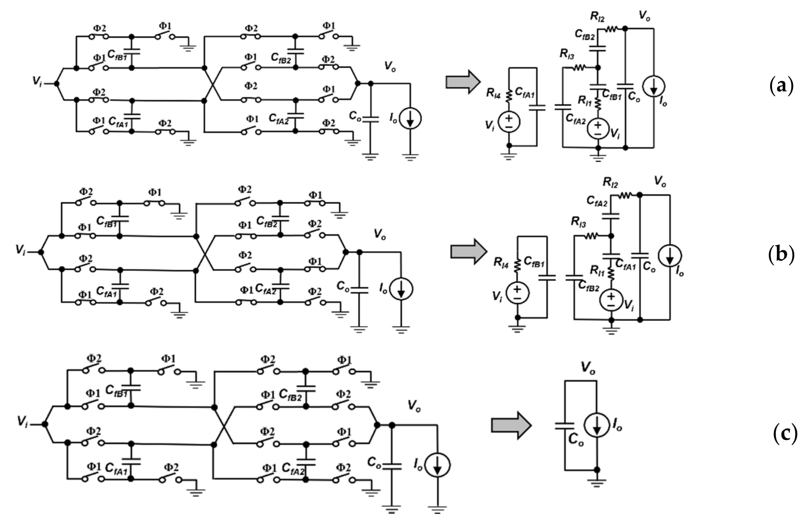
2.3. Proposed Piecewise Modeling of Output-Voltage Ripple for 2-Stage Cross-Coupled Voltage Doubler
To verify the application of proposed piecewise modeling, the analysis is extended to 2-stage cross-coupled voltage doubler.
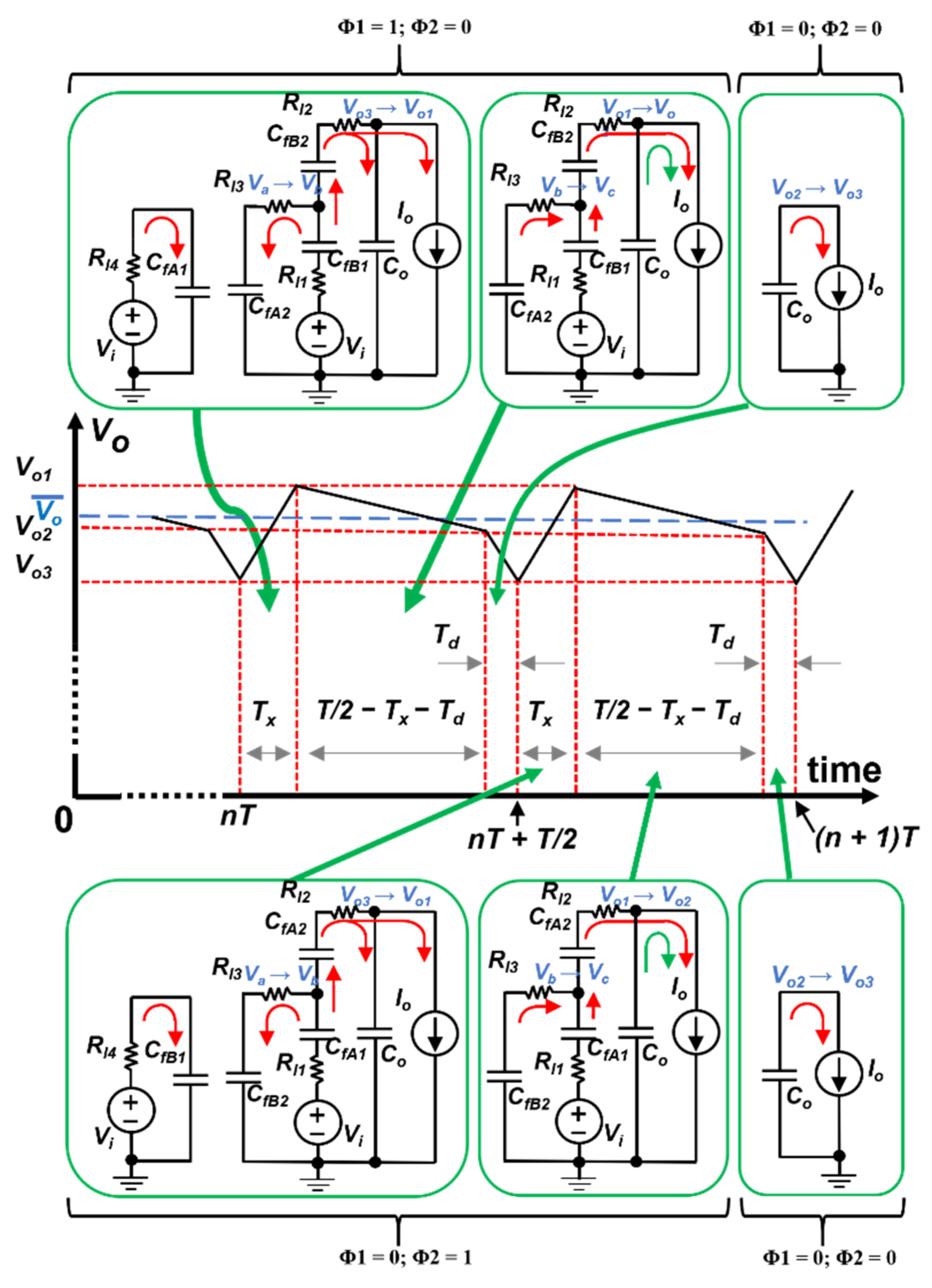
Figure 8 shows the switching behaviors of a 2-stage cross-coupled voltage doubler.
Figure 8a shows the case for Φ1 = 1 and Φ2 = 0,
Figure 8b illustrates the condition for Φ1 = 0 and Φ2 = 1 and
Figure 8c reveals the situation of deadtime when Φ1 = 0 and Φ2 = 0. Since the number of switches in each branch is different, the lump sums of the resistances from switches, routing and bond-wire are noted as
Rl1,
Rl2, and
Rl3. It is noted again that
Td is much shorter than
T.
CfA1 and
CfB1 are the flying capacitors in the first stage, and
CfA2 and
CfB2 are the flying capacitors in the second stage.
Basically, the operations for {Φ1 = 1 and Φ2 = 0} and {Φ1 = 0 and Φ2 = 1} are the same due to the parallel structure. Thus, the corresponding modeling of both cases are the same, except different flying capacitors are used to complete the operation of the circuit. Ideally, from the switching operations, CfA1 and CfB1 are charged to Vi, while CfA2 and CfB2 are charged to 2Vi. Therefore, Vo is 4Vi theoretically, which is the sum of the source voltage and the voltages across CfA1 (or CfB1) and CfA2 (or CfB2). During the deadtime, all switches are turned off to disconnect the output from the flying capacitors and Vi. Thus, the load is supplied.
Figure 9 shows the details of the output waveform of one switching cycle and the corresponding
RC circuits (from
Figure 8) of a 2-stage cross-coupled voltage doubler. The operations at
nT and (
nT +
T/2) are the same, except another half circuit operates alternatively. Thus, the analysis can be conducted for half of a switching cycle. At
nT,
CfB1 and
CfB2 are previously charged to
VCf and about 2
Vi, respectively, at (
(n − 1
)T +
T/2) (i.e., the same operation at (
nT +
T/2).
CfB1 provides charges to
CfA2 to re-charge it to about 2
Vi. Similarly, they supply charges to
Co such that the output increases from
Vo3 to
Vo1. The required time to complete this operation is
Tx. Then, at (
nT +
Tx), the source
Vi,
CfA2,
CfB1,
CfB2 and
Co supply charges to the load. The discharges of flying capacitors and output capacitor decrease the output from
Vo1 to
Vo2. At (
nT +
T/2 −
Td), all switches are turned off. Only
Co supplies charges to the load, and thus the output drops more rapidly than before from
Vo2 to
Vo3. In the above analysis, it is assumed that
T/2 is longer than 6
RlCf2 (where
Cf1 =
CfA1 =
CfB1 and
Cf2 =
CfA2 =
CfB2) to the charge redistribution during
T to
Tx,
T/2 to
T/2 +
Tx, is complete, while
CfA2 and
CfB2 are charged to about 2
Vi at the end of half of a switching cycle.
Based on the
RC circuits in
Figure 9, at (
nT −
Td), the charge redistribution between
CfB1,
CfA2, and
CfB2 is completed. Considering the voltage at the output of the first stage of charge pump is a constant value, the current passing through
CfB2 and
Co is in constant ratio. Hence, the current passing through
CfA2 and
Co can be approximated as
CfA2Io/(
CfA2 +
Co) and
CoIo/(
CfA2 +
Co). Similarly, the current passing through
CfB2 and
CfA1 is
CfA2CfB2Io/(
CfA2 +
Co)/(
CfB2 +
CfA1) and
CfA2CfA1Io/(
CfA2 +
Co)/(
CfB2 +
CfA1). At
nT, the charges stored in
CfA2 and
CfB1 are
CfA2(
Vo2 +
CfA2IoRl2/(
CfA2 +
Co)) and
CfB1VCf1, respectively. It is noted that the negative charges at the bottom plate of
CfB2 should also be considered. Assuming that
Cf1/
Cf2 =
Cf2/
Co =
m2, the highest output voltage of the first and second stage of the charge pump achieves at
Tx1 and
Tx2. According to similar analysis of Equations (14) and (15), it could be seen that
Tx1 and
Tx2 have close values due to the log relationship of
Tx and
m1. Hence, it is reasonable to assume that
Vb and
Vo1 both achieve at (
nT +
Tx). Then, at (
nT +
Tx), the current passing through
CfA2 and
Co is 0. Therefore, the charges remaining in
CfA2,
CfB1 and
CfB2 are
CfA2Vb,
CfB1(
Vb −
Vi +
IoRl1) and
CfB2(
Vo1 −
Vb +
IoRl2), respectively. By the principle of conservation of charges [
7],
Tx could be approximated by
Tx2, which satisfies the following equation.
with
. For simplification of the calculation, the average output voltage value for the first stage
Vi2 is approximated as
Vc, which could be calculated without
Tx, and the related calculation of
Vc is given in the following part.
VCf1 is the voltage obtained by capacitor
CfA1 when charging with an ideal voltage supply
Vi within a time period
T/2. Therefore,
VCf1 is given by
At
nT, the charges in
CfB2 obtained before the deadtime in the previous half of a cycle is
CfB2[Vc +
IoRl3CfA2CfA1Io/(
CfA2 +
Co)/(
CfB2 +
CfA1)], and the charges in
Co is
CoVo3. At (
nT +
Tx), the charges in
CfB2 and
Co are
CfB2(
Vo1 −
Vb +
IoRl2) and
CoVo1, respectively. The charges to the load are
IoTx. Thus, the following relationship is obtained.
Between (
nT +
Tx) and (
nT +
T/2 −
Td), some charges in
CfA2 and
CfB1 go to
CfB2. Since the overall charges in the connection of three capacitors are constant, the following equation is obtained.
Moreover, the net charges of
CfA2 and
Co will supply the load so that the following expression is obtained.
Finally, during the deadtime, the charges from
Co supplies to the load gives the following relationship.
Solving Equations (28)–(34),
Vo1,
Vo2 and
Vo3 could be calculated, and the average value of
Vo is given by
Similar to the analysis of Equation (16), PCE can be easily derived by the ratio of
Eo to
Ei.
where
is found as shown in Equation (35).


