Abstract
In this study, the performance of an organic dye obtained from the bark of the red pine (Pinus brutia) tree growing in Muğla/Turkey as an interface layer in the Au/n-Si Schottky diode (SD) structure was evaluated. For this purpose, at first, the optimized molecular structure, the highest occupied molecular orbital (HOMO), and the lowest unoccupied molecular orbital (LUMO) simulations of the organic dye were calculated by the Gauss program and it was theoretically proven that the dye exhibits semiconducting properties. Then, the electrical and photodiode variables such as ideality factor, effective barrier height, series resistance, interface states density distribution, photosensitivity, and photo responsivity were evaluated employing current-voltage measurements under dark and different illumination densities. Additionally, C-V measurements were used to demonstrate that the fabricated device has capacitive features and this capability varies as a function of the frequency. Under these measurements, the possible conduction mechanism for the organic dye-based Au/n-Si device was investigated and the results showed that Au/Pinus brutia/n-Si may be a good candidate for optoelectronic applications.
1. Introduction
Metal-semiconductor (MS) and metal-interface layer-semiconductor type Schottky barrier diodes (SBDs) have been extensively investigated over the years due to their unique properties for electronic applications, such as fast response, low resistance and low transition reverse current during switching [1,2]. The performance of Schottky barrier diodes is also known to be dependent on the characteristics of the metal/semiconductor junction [3]. Especially in recent years, improvement of interfaces in metal/semiconductor SBDs and novel alternative materials for the interface have been searched for intensively [4,5]. Considering their chemical stability as well as their optical properties, it can be said that organic semiconductors are good candidates for optoelectronic and photonic applications. Indeed, in a previously published study [6], some of the authors of this manuscript emphasized that organic substances are primarily composed of carbon-based molecules and that a wide range of biological materials suitable for electronic applications can be obtained due to these molecules’ ability to form extended polymeric chains. Namely, two major classifications can be made for organic semiconductors as low molecular weight material and polymers. Both have a conjugated π-electron system created by the pz-orbitals of the sp2-hybridized C-atoms of the molecules [7]. Compared to σ-bonds, π-bonds are significantly weaker. Therefore, π-π*-transitions in conjugated molecules generate the lowest electronic excitations, making them suitable for electronic device applications. The energy levels of the molecule grow increasingly dense as more conjugated orbitals become involved. Thus, the electron can be excited and a charge flow can be achieved [8]. In addition, electron displacement along the increasing polymeric chain increases electron conductivity and stability. Many attempts can be found in the literature to improve SBDs’ electrical properties in different electrical applications by using organic semiconductors. As an example, Ongun et al. [9] produced an Au/BOD-Pyr/n-Si/In rectification device and showed that the organic matter of BOD-Pyr has suitable semiconductor features for optoelectronic applications. In another study, Tan et al. [10] conducted a comparative investigation on the effects of organic Metal Polymer Semiconductor (MPS) and inorganic Metal Insulator Semiconductor (MIS) interlayers in Au/n-GaAs Schottky diodes and they observed that MIS structure exhibits better performance although MPS exhibits rectifying properties. They also claimed that the performance of MPS-type SBDs can be enhanced by doping polyvinyl alcohol (PVA) with different elements. Oztürk [11] also investigated the Al/p-Si device in terms of organic/inorganic mixture-based interlayer structures. For this purpose, a phenyl C61-butyric acid methyl ester (PCBM)-doped zinc oxide (ZnO) interlayer was used in an Al/p-Si rectifying device to improve its electrical behavior. As a result, it has been observed that the current in reverse biases increased for the fabricated Al/PCBM:ZnO/p-Si device with increasing light illumination intensity, and it was demonstrated that this device has good potential for optoelectronic applications. Recently, research studies on organic dye/n(p)-Si devices are being stimulated by their high UV absorption and ability to be produced without harmful waste to the environment. For example, Imer et al. [12] investigated Sunset Yellow/n-Si hybrid Schottky diodes and obtained a device very close to the ideal. They also observed that the photoresponsivity of the Sunset Yellow/n-Si device increased with increasing illumination density because of the excited electron-hole pair by the photons. In another study, Sahin et al. [13] used a BODIPY-based dye as an interlayer in the Au/n-Si rectifier and investigated its photodiode performance as a function of illumination intensity. They observed that the ideality factor value of the device exhibits decreasing tendency with increasing illumination density because of the formation of electron-hole pairs by incident photons. El-Mahalawy et al. [14] also studied a phenol-based push-pull azo dye/n-Si device and investigated its suitability in UV photo detection applications. They observed that the reverse current of the fabricated device increased by two orders of magnitude under UV illumination as carriers resulting from photon interaction were swept away by the built-in area of the junction. The purpose of our study was to develop a sustainable, economically inexpensive organic-based electronic device based on an easily available pine resin. Among the three most significant pine species in Turkey, i.e., Pinus sylvestris, Pinus nigra, and Pinus brutia, the last one was selected, because, besides having a fast-growing structure, it has an area of approximately one million hectares in the Mediterranean, Aegean, and Marmara [15]. This findability makes it attractive for researching its suitability in optoelectronic applications. The light response and thus the photodiode properties of the Au/n-Si device, in which the dye produced from the bark of the Turkish pine plant is used as the interface material, were investigated.
2. Materials and Methods
In this study, a Au/Pinus brutia/n-Si device was fabricated by using n-type silicon wafers with (100) orientation, 400 µm thickness, and 1–10 Ω cm resistivity. N-type silicon was chemically cleaned using RCA procedures [16]. A pinus barks dye-based spray solution was prepared by using barks taken from Pinus brutia growing in Muğla/Turkey. The dye was extracted from powdered barks in a hot water bath for 24 h at 60 °C using methanol (4.5 g/30 mL). The resultant extract was filtered via filter paper to achieve the final solution [17]. The composition of OPCs (oligomeric proanthocyanidins) obtained from red pine bark varies according to the method of obtaining it. The OPC used in our research was obtained according to the above procedure. The composition of the product obtained according to this method is given in Table 1. The results are in agreement with the findings in the studies of Yesil-Celiktas et al. [18]. The ingredients of natural products such as Pinus brutia work synergistically, that is, they reinforce each other’s effects. Even when the molecules are purified and used separately, they do not show a healing effect. In photosynthesis, which is a natural light capture process, besides chlorophyll, other photon-capturing organic molecules such as β-carotene and lycopene are known to be used together because they have a synergetic effect and complement each other [19], so the molecules were used together without purification. It is accepted that the molecules in the mixture will complement each other and strengthen their effects. The final solution (30 mL) was sprayed on the pre-cleaned n-Si substrate at a temperature of 400 °C and 2 mL/min spraying rate by using air as the carrier gas. Gold contacts as the working electrode were grown with a total area of 2.27 × 10⁻² cm2 and a thickness of 100 nm in a vacuum atmosphere of 10−5 Torr on Pinus brutia-based dye by thermal evaporation method. In the same way, the device architecture was completed by depositing Al contacts with a 100 nm thickness on the back surface of the Si substrate. The device structure and possible energy diagram of the heterojunction have been illustrated in Figure 1a,b respectively.

Table 1.
Molecular orbital distribution of Pinus brutia (1-9) indicate the number of molecules.

Figure 1.
Schematic diagram of the fabricated device (a) and energy diagram of the heterojunction (b).
The density functional theory (DFT) technique, as implemented in the Gaussian 09W package, was used to optimize the geometry of the molecules. The photodiode properties of the obtained device were evaluated by the current-voltage (I–V) analysis under dark and illumination conditions with a Keithley 2400 source meter. I-V measurements in dark conditions were also carried out at different temperatures in the range of 200–400 K. Capacitance-voltage (C–V) measurements were also conducted with different frequencies under dark conditions using HP 4192A (50 Hz–13 MHz) LF Impedance analyzer.
3. Results and Discussion
3.1. DFT Calculations
Density-functional theory (DFT) is a widely used method to calculate the electronic structure of atoms, molecules, and solids. In this context, density functional theory (DFT) can give a more in-depth knowledge of the connection between molecular structure and compound characteristics [20]. Since we aimed to investigate the sensitivity of Pinus brutia to light within the scope of this study, it was important to investigate the HOMO-LUMO levels, which are the thermodynamic driving force for electron injection, and thus the energy of the bandgap. Table 1 shows the molecular structures that make up Pinus brutia, as well as the geometric shape of the HOMO and LUMO levels. For effective charge transfer, the LUMOs of molecules must be more negative than the semiconductor’s conduction band [21]. As it is known from the literature [7,22], we can provide information about the conductivity of the compound thanks to the electron affinities of the HOMO-LUMO levels. A low HOMO-LUMO gap indicates that the compound is easily excitable and polarizable, while a large HOMO-LUMO gap means that a higher light energy is necessary to excite the electron in the HOMO. Our calculated results are represented in Figure 1b. Pinus brutia appears to be composed of molecular compounds with a bandgap ranging from about 4.1 eV to 6.8 eV. It can be concluded that Pinus brutia has semiconductor properties since these results are in a range comparable to the bandgap values of some metal oxides [23] and organic materials [24] used in optoelectronic applications in the literature. In addition, it can be concluded that dimer structures exhibit the lowest vertical transition energies. This may be related to the decreasing number of monomeric units. This demonstrates that increasing p-conjugation facilitates electron movement from HOMO to LUMO, where the molecular π-π* orbitals are shown. A careful look at the molecular structures of the compounds shows that they correspond to polyhydroxy derivatives. Since it is known that such compounds can be converted to quinones via redox reactions when voltage is applied, the question may come to mind as the results here show the redox behavior of the molecules. Within the scope of this study, it was not examined whether the compounds were converted to quinones. The compounds in our study consisted of catechol-catechol derivatives and taxifolin-taxifolin derivatives.
In a study conducted by Janeiro and Oliveira Brett [25], oxidation of hydroxyl groups to quinone was explained by considering the oxidation mechanism of catechin, shown in Figure 2, whose A, B and C rings are resorcinol, catechol and hydroxyl groups, respectively. Accordingly, the 3′ and 4′ hydroxyl groups in the B ring of catechin are oxidized to the quinone depending on the pH of the medium. Other hydroxyl groups are not affected. Similar reaction can be predicted in taxifolin. However, this redox reaction takes place in aqueous media depending on the pH, while our reaction medium is dry.
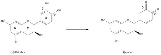

Figure 2.
Catechin oxidation mechanism.
3.2. Au/n-Si and Au/Pinus brutia/n-Si Devices Performaces
Figure 3a shows the measured semi-log I-V curves of both Au/n-Si and Au/Pinus brutia/n-Si Schottky junctions under the dark condition at room temperature. Here, when the dye is in close contact with the silicon, the silicon is depleted from its carriers near the interface and the thermal energy becomes higher than kT. Therefore, the device starts to show rectifying properties, as demonstrated by the asymmetrical behavior of I-V curves shown in Figure 3a [25]. Additionally, it can be concluded that the organic layer improves the rectifier characteristic of the Au/n-Si device, as well as the series resistance effect at high voltage values. To examine the effect of the organic layer in detail, equations of the standard Thermionic Emission (TE) theory can be used. According to TE theory, the relationship between current and voltage is [26]:
where q, V, k, I0 and η represent the electron charge, the bias voltage, the Boltzmann constant, the saturation current at reverse bias and the ideality factor, respectively.

Figure 3.
Relative energy positions of HOMO-LUMO energy vs. number of molecules (a) and comparison of I-V characteristics of Au/n-Si and Au/Pinus brutia/n-Si devices (b).
The , , T (300 K), A (7.85 × 10⁻³ cm2), A* (112A cm−2 K−2 for n-type silicon) symbols given in Equations (2) and (3) are the slope obtained from the linear region of ln(I) vs. V, the effective barrier height, the operation temperature, the effective diode area, and the Richardson constant, respectively. Using the equations given above, ideality factor () and effective barrier height ( values were found to be 2.35 and 0.58 eV for Au/n-Si, and 2.12 and 0.65 eV for Au/Pinus brutia/n-Si, respectively. For an ideal Schottky type junction, the ideality factor value is 1. As seen above, the ideality factor values calculated for both devices are greater than unity. In previously published papers [27,28,29,30] about metal-semiconductor junctions, the greater value of the ideality factor was attributed to the distribution of the metal-semiconductor interface states, image force effect, recombination-generation process, and different transport mechanisms besides the TE. In our Au/Pinus brutia/n-Si device, the lower ideality factor value is directly linked to the presence of the pine-based dye layer. In the literature [31,32,33], it is possible to find studies in which the ideality factor value both increases and decreases as a result of the integration of the organic-inorganic layer between the metal and semiconductor. In [34,35], the increase in the ideality factor with the presence of organic layers was attributed to the interface mechanisms that contain interface dipoles due to the organic layer as well as the distribution of density of interface states as a result of the fabrication-related defects in the interface. Furthermore, Zahn et al. [36] stated that the increase or decrease in the effective barrier height and thus the ideality factor caused by the organic interlayer is associated with the energy level alignment of the lowest unoccupied molecular orbital with respect to the inorganic semiconductor’s minimum conduction band at the organic/inorganic semiconductor interface. Other authors attribute the decrease in the ideality factor value to modification of the interfacial potential barrier depending on the organic dye layer [35,37]. That is, the Pinus brutia dye interlayer affects the space charge region of the n-type silicon and increases the effective barrier height by changing the density of interface distribution between n-type Si and Au, therefore causing a reduction in the ideality factor. In addition, interface states resulting from the presence of the organic layer may behave as a trap. Thus, the Fermi level can be shifted towards the middle of the bandgap of the organic dye layer. Therefore, the barrier height may not have a homogeneous nature, considering that the Fermi level can change its position throughout the whole dye layer. Similar results were also found by other researchers to explain potential shifts due to the organic layer [38]. In this study, we investigated the performances of the Au/Pinus brutia/n-Si device under both dark and light conditions, in view of its potential optoelectronic applications.
Figure 4a compares the I-V characteristic of the Au/Pinus brutia/n-Si junction in dark and illumination (400 mW/cm2) conditions at room temperature. As can be seen, the reverse current under illumination shows an increasing trend with respect to the dark state. This can be explained by considering the formation of electron holes in n-type Si. That is, the incoming photons pass through the Pinus brutia dye without absorption and, being absorbed in the n-Si, originate electron-hole pairs (see Figure 1b) [39]. Because of this, the photocurrent is observed in the reverse bias under illumination conditions. To get information about the effect of illumination on the diode performances, we obtained some diode characteristics such as ideality factor value and effective barrier height for the Au/Pinus brutia/n-Si device under illumination conditions. The ideality factor and the barrier height values, as obtained by using Equations (1)–(3) are 2.81 and 0.67 eV, respectively. Under illumination, the ideality factor of the devices increases with respect to the dark value. A value indicates that leakage currents are dominant in the transport mechanisms of the devices [40]. That is, when the ideality factor values are greater than 2, tunneling improves interface recombination and becomes dominant for the current transport [41]. Moreover, it can be observed that not only the value of the ideality factor increases but also the values of leakage current, which probably indicates that the illumination affects the interface recombination of photo-generated carriers at the junction interface [42]. The calculated leakage current for the Au/Pinus brutia/n-Si device is 1.13 × 10⁻⁸ A and 9.70 × 10⁻⁷ A for dark and illumination conditions, respectively, in accordance with the aforementioned conclusion. In addition, generally, there is a reverse relationship between variation in ideality factor values and effective barrier height values [43,44], not observed for our device under illumination. This inconsistency may be associated with inhomogeneous barrier height, non-uniformity of dye layer, presence of interfacial oxide layer, and distribution of interfacial charge as a result of the illumination at the dye and n-Si interface [45]. In addition, I-V analyses of the Au/p-Si device at three different temperatures were performed to obtain more detailed information about the device’s conduction mechanism. Results of I-V measurements are shown in Figure 4b. As is known, thermionic emission theory is typically used to investigate the influence of temperature fluctuations on the ideality factor and effective barrier height of devices [46]. In practice, Schottky barrier devices operate at temperatures ranging from low to high (depending on the power application) [47]. In our study, measurements were taken at different temperatures between 200 K and 400 K with 100 K steps. The experimental values of and at each temperature were determined from the slope and intercept of the log (I) vs V plot. The Au/Pinus brutia/n-Si device values are = 3.39 and = 0.53 eV at 200 K, and = 1.65 and = 0.97 eV at 400 K. At lower temperatures, electrons surpass the lower barriers in this process. As a result, the current flowing through patches with a lower Schottky barrier height and a higher ideality factor dominate the current transport phenomenon [48]. As the temperature rises, a greater number of electrons have sufficient energy to overcome the higher barrier, resulting in an increased barrier height with rising temperature and bias voltage. Additionally, there is a significant deviation from linearity that is observed in the forward bias I-V characteristic. This is usually explained due to the effect of series resistance (Rs) originated by the presence of interface defects states and the interface layer [49]. In this context, a modified Norde approximation has been used to determine barrier height and series resistance values. According to this approximation, the following equations are used:
where F(V0) and indicate the minimum value in F(V) vs. V curve and first integer value following the ideality factor value, while V0 is the corresponding bias. After drawing F(V)-V curves according to Equation (4), the barrier height and series resistance values can be calculated.
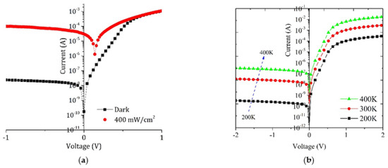
Figure 4.
I-V characteristic of the Au/Pinus brutia/n-Si device in dark and light conditions (a) and in dark at different temperatures (b).
Figure 5 represents F(V) vs. V curves of the Au/Pinus brutia/n-Si device under dark and illumination conditions. The obtained barrier height values were 0.94 eV and 0.72 eV for dark and illumination conditions, respectively. In addition, Rs values were obtained by using Figure 2 and the following Equation:
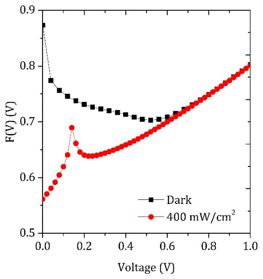
Figure 5.
F(V) vs. V curves of the Au/Pinus brutia/n-Si device under dark and illumination.
From Equation (6), the Rs values were calculated as 221 Ω and 188 Ω for dark and illumination conditions. The increase in carrier density as a result of illumination can be seen as a possible reason for the decrease in the series resistance of the for the Au/Pinus brutia/n-Si device under illumination conditions [50]. The Cheung method can be also used to determine the diode characteristics, i.e., ideality factor, barrier height, and Rs values of the studied device, basing on the following equations:
Figure 6 is drawn on the basis of Equations (7) and (8). From Figure 6, it is possible to infer the ideality factor, the barrier height and the series resistance (Rs) of the investigated devices. For this aim, it is necessary to use the slope and y-intercept of the dV/dln(I) for determining the ideality factor and series resistance values, while considering the y-axis intercept and slope of H(I) plots makes it possible to obtain barrier height and series resistance of the device [51].
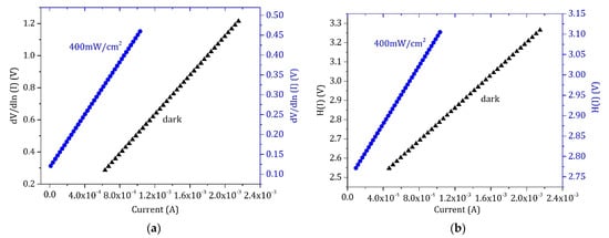
Figure 6.
Plots of dV/dln(I) vs. (I) (a) and H(I) vs. (I) (b) for the Au/Pinus brutia/n-Si device under dark and illumination condition.
The diode parameters calculated from Equations (7) and (8) and Figure 6 are reported in Table 2. Two conclusions can be made from the tabulated results. First, similar to the previous calculations based on TE and Norde models, Cheung approximations give the same trend in ideality factor, series resistance and barrier height values. This shows that there is a consistency in the diode characteristics obtained by the different models. Second, there is a significant difference between the ideality factor values obtained by TE and Cheung approximation. This can be explained by the effect of series resistance, voltage drop through the Pinus brutia dye layer, bias dependence of the Schottky contact, and variation in density of interface states in the concave region of the I-V curves [52,53]. Although, the series resistance value of the device exhibited decreasing tendency under illumination conditions if compared with the values obtained under dark conditions, their absolute values are different. In fact, the series resistances obtained by the Norde method are lower than the values obtained from the Cheung method. This discrepancy can be clarified as follows.
Table 2.
Experimentally calculated ideality factor, barrier height, and series resistance of the Au/Pinus brutia/n-Si device.
The Norde function uses full-forward bias I-V data to calculate the diode parameters, while the Cheung method uses data in the nonlinear region where the series resistance effect is observed. In other words, the Norde approach is a more suitable method for devices close to ideality. Similar differences obtained by different methods were also observed by other authors [54].
The density of interface states is an important way of understanding the nature of the metal-semiconductor junction. For this reason, the effect of light on the interface states of the Au/Pinus brutia/n-Si device was investigated. Similar to our previously published results [55], the distribution of interface states (Nss) between junction materials has been inferred by forward bias I-V measurements, by considering the voltage dependence of the ideality factor. This is given by:
where , , and are the permittivity of the interfacial layer, the permittivity of the semiconductor, the estimated thickness of the interfacial layer, and the depletion layer width, respectively. Thus, voltage dependent Nss values may be written as:
Equation (10) allows us to draw the distribution of interface states vs. conduction band edge of the semiconductor. Therefore, energy differences between conduction band edge-surface can be calculated by the following formula.
Figure 7 shows Nss vs. Ec-Ess plots of the Au/Pinus brutia/n-Si device. As can be observed in Figure 7, Nss decreases from 2.099 × 10¹⁵ to 4.429 × 10¹⁴ in the range of 0.426 eV and 0.521 eV in illumination conditions, while it decreases from 4.268 × 10¹⁵ to 1.587 × 10¹⁵ in the range of 0.401 and 0.447 eV in the dark condition. In addition, it can be observed that the density of interface states exhibits decreasing tendency compared with the values obtained under dark conditions. These variations may be linked with the decrease in recombination centers and reordering interfacial states in the Pinus brutia layer. Based on the Pinus brutia-based device photoresponse, we can conclude that it is suitable for photodetector applications. The current-voltage characteristics of the device were measured under different illumination intensities to get a detailed analysis of the photodiode characteristics of the device and the results are shown in Figure 6.
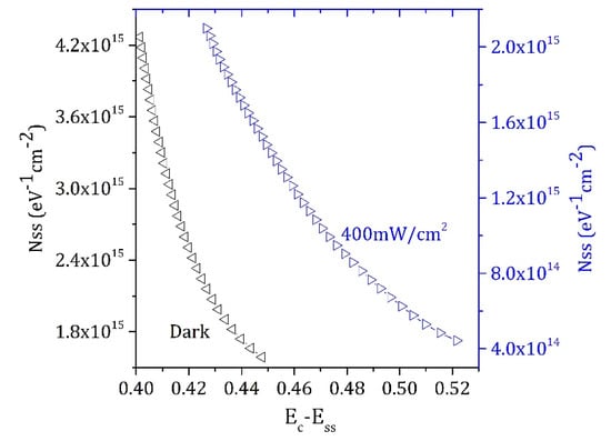
Figure 7.
Nss vs. Ec-Ess plots for Au/Pinus brutia/n-Si device under dark and illumination condition.
Photocurrent and photosensitivity are important parameters for a photodetector. In our device, the current under illumination is significantly higher than the dark current at the same voltage, which shows that the photodetector responds well to incoming light and possesses strong photoelectric conversion ability. The variation in the photocurrent at 1 V as a function of illumination intensities is given in Figure 8. Following the above discussion, the photocurrent values obtained at +1 V exhibit increasing tendency as a function of illumination intensities. The photosensitivity S of the studied detector can be determined by Equation (12):
where and are the photocurrent and dark currents, respectively, for reverse biases. For photodiodes or detectors, there is a relationship between the photocurrent and the light power (P) given by [56]. In this equation, B indicates a constant, while indicates a photoconduction mechanism. can be determined by the slope of the photocurrent plot and in our case is 1.38. Similar to the study made by Shiu et al., it can be concluded that this non-integer exponent may be related to the complex process of electron-hole generation, trapping, and recombination with the topological insulator [57]. The photosensitivity S and the photocurrent , the latter calculated according to the formula are shown in Figure 9 under different illumination intensities.
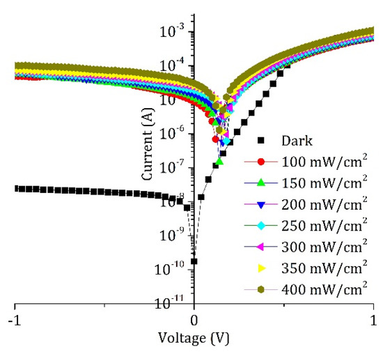
Figure 8.
I-V characteristic of the Au/Pinus brutia/n-Si device under different illumination intensities.
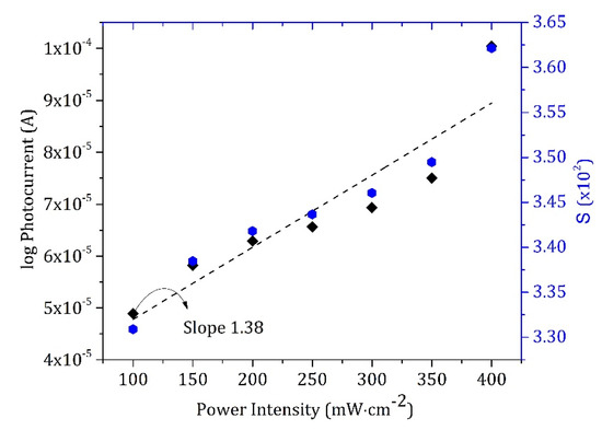
Figure 9.
Variation of photocurrent and photosensitivity of the Au/Pinus brutia/n-Si device as a function of illumination intensities.
The photo responsivity value (R) of a photodiode or detector can be seen as another important parameter and can be obtained from the relationship below:
where P is the incident illumination power density and A is the effective diode area.
The variation in the photoresponsivity of the device as a function of illumination intensities under the reverse bias condition is shown in Figure 10. From Figure 10, it is seen that the photoresponsivity of the device shows decreasing tendency with the increasing illumination condition. This case is frequently observed in organic-based photodiodes [57,58] and attributed to the enhancing recombination under high illumination densities [59].
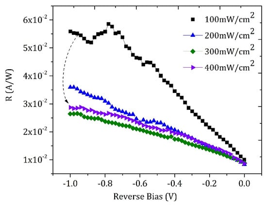
Figure 10.
Calculated responsivity (R) of Au/Pinus brutia/n-Si vs. the reverse bias at various light intensities.
The carrier density of the fabricated device was calculated from the C-V curves. C-V measurements were taken by superimposing an ac signal into a dc biased device. Therefore, all curve change depends on the frequency. In addition, it can be seen from the graphs that capacitance increases with bias at low frequencies, and decreases at high frequencies. For this reason, we made our analysis by considering 500 kHz as the frequency value by using a 1/C2 graph (inset of Figure 11), as in our previous studies on a different junction [60,61]. Diffusion potential and acceptor carrier concentration were found to be 0.75 V and 1.5 × 1015 cm−3, respectively. The obtained carrier concentration value is in the normal range of typical semiconductors for such applications [50,62]. In addition, from the C-V curves the barrier height value of the Au/Pinus brutia/n-Si device was determined as 0.93 eV, which is considerably higher if compared with the one obtained from I-V measurements. This result can be explained by the non-homogeneous nature of the barrier height formed due to the presence of the interface oxide layer on the n-Si wafer and the non-uniformity of the interface layer [51].
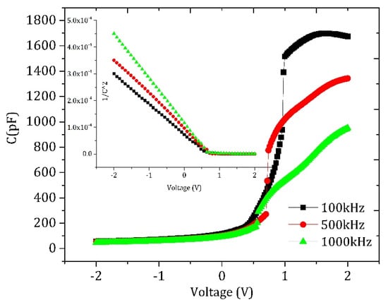
Figure 11.
C-V characteristics of the Au/Pinus brutia/n-Si device under both reverse and forward bias. Inset shows the 1/C2 curves vs. V.
4. Conclusions
In this study, Au/Pinus brutia/n-Si device architecture was obtained by using an economically inexpensive homemade spray pyrolysis technique. For this purpose, a homogeneous solution was obtained by an organic dye from red pine (Pinus brutia) grown in Muğla/Turkey, using methanol as solvent. The solution was sprayed onto a n-Si substrate heated at 400 °C. Gold dot contacts were deposited on the organic dye, and the device structure was completed by using Al contacts on the n-Si. Dye molecular structure and compound characteristics were evaluated using DFT calculations. From the DFT calculations, it was found that Pinus brutia is composed of molecular compounds with a bandgap in the range of 4.1 eV–6.8 eV. The junction parameters of the device, such as the ideality factor values and barrier height, exhibit different tendencies under dark and 400 mW/cm2 illumination conditions. It was also observed that (Nss) decreased from 2.099 × 10¹⁵ to 4.429 × 10¹⁴ in the range of 0.426 eV and 0.521eV in illumination conditions, while Nss decreased from 4.268 × 10¹⁵ to 1.587 × 10¹⁵ in the range of 0.401 and 0.447 eV in the dark conditions. The response of the device to light was also investigated using photosensitivity and photoresponsivity measurements. Results showed that the conduction mechanism of the Au/Pinus brutia/n-Si device may be explained by several mechanisms: electron-hole generation, trapping, and recombination through the topological insulator. Diffusion potential and acceptor carrier concentration were also inferred by C-V analysis and found to be 0.75 V and 1.5 × 1015 cm3, respectively. All the results show that the Pinus brutia dye is a good candidate for optoelectronic applications.
Author Contributions
Investigation and methodology, M.Y., Y.D., S.A. and M.L.G.; writing—original draft preparation, M.Y., S.A. and M.L.G.; writing—review and editing, M.Y. and M.L.G. All authors have read and agreed to the published version of the manuscript.
Funding
This research received no external funding.
Data Availability Statement
Data are available on request from the authors.
Acknowledgments
COST INNOVATORS GRANT IG15102 ITHACA, is gratefully acknowledged.
Conflicts of Interest
The authors declare no conflict of interest.
References
- Lin, Y.-K.; Hong, Y.-T.; Shyue, J.-J.; Hsueh, C.-H. Construction of Schottky junction solar cell using silicon nanowires and multi-layered graphene. Superlattices Microstruct. 2018, 126, 42–48. [Google Scholar] [CrossRef]
- Yahya, A.H.; Klein, A.; Balal, N.; Borodin, D.; Friedman, A. Comparison between Up-Conversion Detection in Glow-Discharge Detectors and the Schottky Diode for MMW/THz High-Power Single Pulse. Appl. Sci. 2021, 11, 4172. [Google Scholar] [CrossRef]
- Ahmad, Z.; Sayyad, M.H. Extraction of electronic parameters of Schottky diode based on an organic semiconductor methyl-red. Phys. E Low-Dimens. Syst. Nanostruct. 2009, 41, 631–634. [Google Scholar] [CrossRef]
- Çetinkaya, H.; Demirezen, S.; Yerişkin, S.A. Electrical parameters of Au/(%1Ni-PVA)/n-Si (MPS) structure: Surface states and their lifetimes. Phys. B Condens. Matter 2021, 621, 413207. [Google Scholar] [CrossRef]
- Kim, H.J.; Park, S.P.; Min, W.K.; Kim, D.; Park, K.; Kim, H.J. Modulation of the Al/Cu2O Schottky Barrier Height for p-Type Oxide TFTs Using a Polyethylenimine Interlayer. ACS Appl. Mater. Interfaces 2021, 13, 31077–31085. [Google Scholar] [CrossRef]
- Daş, E.; Incekara, U.; Aydoğan, Ş. A comparative study on electrical characteristics of Ni/n-Si and Ni/p-Si Schottky diodes with Pinus Sylvestris Resin interfacial layer in dark and under illumination at room temperature. Opt. Mater. 2021, 119, 111380. [Google Scholar] [CrossRef]
- Brütting, W. Introduction to the Physics of Organic Semiconductors. In Physics of Organic Semiconductors; FRG: Wiley-VCH Verlag GmbH & Co. KGaA: Weinheim, Germany, 2006; pp. 1–14. [Google Scholar] [CrossRef]
- Zhenghao, M. Molecular Structures and Device Properties of Organic Solar Cells; Case Western Reserve University: Cleveland, OH, USA, 2014. [Google Scholar]
- Ongun, O.; Taşcı, E.; Emrullahoğlu, M.; Akın, Ü.; Tuğluoğlu, N.; Eymur, S. Fabrication, illumination dependent electrical and photovoltaic properties of Au/BOD-Pyr/n-Si/In schottky diode. J. Mater. Sci. Mater. Electron. 2021, 32, 15707–15717. [Google Scholar] [CrossRef]
- Tan, S.O.; Tecimer, H.; Çiçek, O. Comparative Investigation on the Effects of Organic and Inorganic Interlayers in Au/n-GaAs Schottky Diodes. IEEE Trans. Electron Devices 2017, 64, 984–990. [Google Scholar] [CrossRef]
- Öztürk, T. Effect of various PCBM doping on the interfacial layer of Al/PCBM:ZnO/p-Si photodiodes. J. Mater. Sci. Mater. Electron. 2021, 32, 10180–10193. [Google Scholar] [CrossRef]
- Imer, A.G.; Kaya, E.; Dere, A.; Al-Sehemi, A.G.; Al-Ghamdi, A.A.; Karabulut, A.; Yakuphanoglu, F. Illumination impact on the electrical characteristics of Au/Sunset Yellow/n-Si/Au hybrid Schottky diode. J. Mater. Sci. Mater. Electron. 2020, 31, 14665–14673. [Google Scholar] [CrossRef]
- Şahin, M.F.; Taşcı, E.; Emrullahoğlu, M.; Gökce, H.; Tuğluoğlu, N.; Eymur, S. Electrical, photodiode, and DFT studies of newly synthesized π-conjugated BODIPY dye-based Au/BOD-Dim/n-Si device. Phys. B Condens. Matter 2021, 614, 413029. [Google Scholar] [CrossRef]
- El-Mahalawy, A.M.; Abdou, M.M.; Wassel, A.R. Structural, spectroscopic and electrical investigations of novel organic thin films bearing push-pull azo—Phenol dye for UV photodetection applications. Spectrochim. Acta Part A Mol. Biomol. Spectrosc. 2020, 248, 119243. [Google Scholar] [CrossRef]
- Şensöz, S.; Can, M. Pyrolysis of Pine (Pinus Brutia Ten.) Chips: 1. Effect of Pyrolysis Temperature and Heating Rate on the Product Yields. Energy Sources 2002, 24, 347–355. [Google Scholar] [CrossRef]
- Kern, W.; Puotinen, D. Cleaning Solutions Based on Hydrogen for Use in Silicon Semiconductor Technology. RCA Rev. 1970, 31, 187–205. [Google Scholar]
- Verenkar, N.; Krishnana, S. Extraction of natural dye from Mammea suriga and its application on silk and cotton fabrics. Indian J. Fibre Text Res. 2020, 45, 402–410. [Google Scholar]
- Yesil-Celiktas, O.; Ganzera, M.; Akgun, I.; Sevimli, C.; Korkmaz, K.S.; Bedir, E. Determination of polyphenolic constituents and biological activities of bark extracts from different Pinus species. J. Sci. Food Agric. 2009, 89, 1339–1345. [Google Scholar] [CrossRef]
- Zulfiqar, S.; Sharif, S.; Saeed, M.; Tahir, A. Role of Carotenoids in Photosynthesis. In Carotenoids: Structure and Function in the Human Body; Springer International Publishing: Cham, Switzerland, 2021; pp. 147–187. [Google Scholar] [CrossRef]
- Mehmood, U.; Hussein, I.A.; Harrabi, K.; Reddy, B.V.S. Density functional theory study on dye-sensitized solar cells using oxadiazole-based dyes. J. Photon. Energy 2015, 5, 053097. [Google Scholar] [CrossRef]
- Mehmood, U.; Hussein, I.A.; Harrabi, K.; Mekki, M.; Ahmed, S.; Tabet, N. Hybrid TiO2–multiwall carbon nanotube (MWCNTs) photoanodes for efficient dye sensitized solar cells (DSSCs). Sol. Energy Mater. Sol. Cells 2015, 140, 174–179. [Google Scholar] [CrossRef]
- Kaplan, N.; Taşcı, E.; Emrullahoğlu, M.; Gökce, H.; Tuğluoğlu, N.; Eymur, S. Analysis of illumination dependent electrical characteristics of α- styryl substituted BODIPY dye-based hybrid heterojunction. J. Mater. Sci. Mater. Electron. 2021, 32, 16738–16747. [Google Scholar] [CrossRef]
- Wang, D.; Narusawa, T.; Kawaharamura, T.; Furuta, M.; Li, C. Influence of sputtering pressure on band gap of Zn1−xMgxO thin films prepared by radio frequency magnetron sputtering. J. Vac. Sci. Technol. B 2011, 29, 051205. [Google Scholar] [CrossRef]
- Costa, J.C.; Taveira, R.J.; Lima, C.F.R.A.C.; Mendes, A.; Santos, L.M. Optical band gaps of organic semiconductor materials. Opt. Mater. 2016, 58, 51–60. [Google Scholar] [CrossRef]
- Janeiro, P.; Brett, A.M.O. Catechin electrochemical oxidation mechanisms. Anal. Chim. Acta 2004, 518, 109–115. [Google Scholar] [CrossRef]
- Sharma, S.N.; Periasamy, C. A study on the electrical characteristic of n-ZnO/p-Si heterojunction diode prepared by vacuum coating technique. Superlattices Microstruct. 2014, 73, 12–21. [Google Scholar] [CrossRef]
- Nasim, F.; Bhatti, A. Influence of different metal over-layers on the electrical behaviour of the MIS Schottky diodes. Int. J. Electron. 2013, 100, 1228–1239. [Google Scholar] [CrossRef]
- Tataroğlu, A.; Altındal, Ş. Analysis of interface states and series resistance of MIS Schottky diodes using the current–voltage (I–V) characteristics. Microelectron. Eng. 2008, 85, 233–237. [Google Scholar] [CrossRef]
- Ocak, Y.; Genisel, M.; Kılıçoğlu, T. Ta/Si Schottky diodes fabricated by magnetron sputtering technique. Microelectron. Eng. 2010, 87, 2338–2342. [Google Scholar] [CrossRef]
- Wetzelaer, G.A.H.; Kuik, M.; Lenes, M.; Blom, P.W.M. Origin of the dark-current ideality factor in polymer: Fullerene bulk heterojunction solar cells. Appl. Phys. Lett. 2011, 99, 153506. [Google Scholar] [CrossRef]
- Mahato, S.; Puigdollers, J. Temperature dependent current-voltage characteristics of Au/n-Si Schottky barrier diodes and the effect of transition metal oxides as an interface layer. Phys. B Condens. Matter 2018, 530, 327–335. [Google Scholar] [CrossRef]
- Güllü, Ö.; Türüt, A. Electronic parameters of MIS Schottky diodes with DNA biopolymer interlayer. Mater. Sci. 2015, 33, 593–600. [Google Scholar] [CrossRef]
- Duman, S.; Turgut, G.; Ozcelik, F.S.; Gürbulak, B. Electrical properties of Al/p–Ge and Al/Methyl Green/p–Ge diodes. Philos. Mag. 2015, 95, 1646–1655. [Google Scholar] [CrossRef]
- Güllü, Ö.; Çankaya, M.; Biber, M.; Türüt, A. Fabrication and electrical properties of organic-on-inorganic Schottky devices. J. Phys. Condens. Matter 2008, 20, 215210. [Google Scholar] [CrossRef]
- Güllü, Ö. Barrier Modification by Methyl Violet Organic Dye Molecules of Ag/P-Inp Structures. Eur. J. Interdiscip. Stud. 2016, 5. [Google Scholar] [CrossRef][Green Version]
- Zahn, D.R.; Kampen, T.U.; Méndez, H. Transport gap of organic semiconductors in organic modified Schottky contacts. Appl. Surf. Sci. 2003, 212–213, 423–427. [Google Scholar] [CrossRef]
- Demir, H.O.; Caldıran, Z.; Meral, K.; Şahin, Y.; Acar, M.; Aydogan, S. The effect of temperature on the electrical characterization of a poly(phenoxy-imine)/p-silicon heterojunction. e-Polymers 2016, 16, 75–82. [Google Scholar] [CrossRef]
- Kampen, T.; Bekkali, A.; Thurzo, I.; Zahn, D.R.; Bolognesi, A.; Ziller, T.; Di Carlo, A.; Lugli, P. Barrier heights of organic modified Schottky contacts: Theory and experiment. Appl. Surf. Sci. 2004, 234, 313–320. [Google Scholar] [CrossRef]
- Gezgin, S.Y.; Kepceoğlu, A.; Toprak, A.; Gündoğdu, Y.; Kiliç, H.Ş. Diode Property Of n-ZnO/p-Si Heterojunction Structure in the Dark and Illumination Condition. J. Selcuk 2018, 17, 19–30. [Google Scholar]
- Sharma, S.K.; Singh, S.P.; Kim, D.Y. Fabrication of the heterojunction diode from Y-doped ZnO thin films on p-Si substrates by sol-gel method. Solid State Commun. 2018, 270, 124–129. [Google Scholar] [CrossRef]
- Nadenau, V.; Rau, U.; Jasenek, A.; Schock, H.W. Electronic properties of CuGaSe2-based heterojunction solar cells. Part I. Transport analysis. J. Appl. Phys. 2000, 87, 584–593. [Google Scholar] [CrossRef]
- Bayhan, H.; Bayhan, M. A simple approach to determine the solar cell diode ideality factor under illumination. Sol. Energy 2011, 85, 769–775. [Google Scholar] [CrossRef]
- Aydoğan, Ş.; Yilmaz, M.; Çaldıran, Z. Improving the rectifying properties of metal/semiconductor junction using novel material: Zam-zam. Sensors Actuators A Phys. 2016, 248, 22–28. [Google Scholar] [CrossRef]
- Kim, S.H.; Jung, C.Y.; Kim, H.; Cho, Y.; Kim, D.-W. Forward Current Transport Mechanism of Cu Schottky Barrier Formed on n-type Ge Wafer. Trans. Electr. Electron. Mater. 2015, 16, 151–155. [Google Scholar] [CrossRef]
- Çaldıran, Z.; Biber, M.; Metin, O.; Aydoğan, Ş. Improving the performance of the organic solar cell and the inorganic heterojunction devices using monodisperse Fe3O4 nanoparticles. Optik 2017, 142, 134–143. [Google Scholar] [CrossRef]
- Sitek, A.; Torfason, K.; Manolescu, A.; Valfells, Á. Space-Charge Effects in the Field-Assisted Thermionic Emission from Nonuniform Cathodes. Phys. Rev. Appl. 2021, 15, 014040. [Google Scholar] [CrossRef]
- Patel, H.; Patel, K.; Patel, A.; Jagani, H.; Solanki, G.K.; Pathak, V.M. Temperature-Dependent I–V Characteristics of In/p-SnSe Schottky Diode. J. Electron. Mater. 2021, 50, 5217–5225. [Google Scholar] [CrossRef]
- Gümuüş, A.; Turut, A.; Yalcin, N. Temperature dependent barrier characteristics of CrNiCo alloy Schottky contacts on n-type molecular-beam epitaxy GaAs. J. Appl. Phys. 2002, 91, 245. [Google Scholar] [CrossRef]
- Singh, J.; Singh, R.G.; Gautam, S.K.; Singh, F. Multifunctional hybrid diode: Study of photoresponse, high responsivity, and charge injection mechanisms. J. Appl. Phys. 2018, 123, 174503. [Google Scholar] [CrossRef]
- Minemoto, T.; Okamoto, C.; Kawai, H.; Murozono, M.; Takakura, H.; Hamakawa, Y. Effect of bulk resistivity on the performance of spherical Si solar cells. In Proceedings of the 2006 IEEE 4th World Conference on Photovoltaic Energy Conference, Waikoloa, HI, USA, 7–12 May 2006; pp. 1081–1084. [Google Scholar] [CrossRef]
- Olyaee, H.G.B.; Foot, P.J.S.; Montgomery, V. Electrical properties and I–V characteristics of 5,14-dihydro-5,7,12,14-tetraazapentacene doped Schottky barrier diode. J. Theor. Appl. Phys. 2015, 9, 315–319. [Google Scholar] [CrossRef]
- Güler, G.; Güllü, Ö.; Karataş, Ş.; Bakkaloğlu, Ö.F. Analysis of the series resistance and interface state densities in metal semiconductor structures. J. Phys. Conf. Ser. 2009, 153. [Google Scholar] [CrossRef]
- Aldemir, D.A.; Kökce, A.; Özdemir, A.F. Schottky diyot parametrelerini belirlemede kullanılan metotların geniş bir sıcaklık aralığı için kıyaslanması. Sak. Univ. J. Sci. 2017, 21, 1. [Google Scholar] [CrossRef][Green Version]
- Sönmezoğlu, S.; Şenkul, S.; Taş, R.; Çankaya, G.; Can, M. Electrical and interface state density properties of polyaniline–poly-3-methyl thiophene blend/p-Si Schottky barrier diode. Solid State Sci. 2010, 12, 706–711. [Google Scholar] [CrossRef]
- Yilmaz, M.; Kocyigit, A.; Çırak, B.B.; Kacus, H.; Incekara, U.; Aydogan, S. The comparison of Co/hematoxylin/n-Si and Co/hematoxylin/p-Si devices as rectifier for a wide range temperature. Mater. Sci. Semicond. Process. 2020, 113, 105039. [Google Scholar] [CrossRef]
- Şahin, M.; Kaplan, R. Intensity and temperature dependence of photocurrent of a-Si:H Schottky diodes. Curr. Appl. Phys. 2006, 6, 114–118. [Google Scholar] [CrossRef]
- Huang, S.-M.; Huang, S.-J.; Yan, Y.-J.; Yu, S.-H.; Chou, M.; Yang, H.-W.; Chang, Y.-S.; Chen, R.-S. Highly responsive photoconductance in a Sb2SeTe2 topological insulator nanosheet at room temperature. RSC Adv. 2017, 7, 39057–39062. [Google Scholar] [CrossRef]
- Yuan, S.; Zhang, H.; Wang, P.; Ling, L.; Tu, L.; Lu, H.; Wang, J.; Zhan, Y.; Zheng, L. High-gain broadband organolead trihalide perovskite photodetector based on a bipolar heterojunction phototransistor. Org. Electron. 2018, 57, 7–13. [Google Scholar] [CrossRef]
- Han, Q.; Bae, S.; Sun, P.; Hsieh, Y.; Yang, Y.; Rim, Y.S.; Zhao, H.; Chen, Q.; Shi, W.; Li, G. Single Crystal Formamidinium Lead Iodide (FAPbI 3): Insight into the Structural, Optical, and Electrical Properties. Adv. Mater. 2016, 28, 2253–2258. [Google Scholar] [CrossRef] [PubMed]
- Grilli, M.L.; Aydogan, S.; Yilmaz, M. A study on non-stoichiometric p-NiOx/n-Si heterojunction diode fabricated by RF sputtering: Determination of diode parameters. Superlattices Microstruct. 2016, 100, 924–933. [Google Scholar] [CrossRef]
- Aytac, Y. Time-Resolved Measurements of Charge Carrier Dynamics in MWIR to LWIR InAs/InAsSb Superlattices. Ph.D. Thesis, The University of Iowa, Iowa City, IA, USA, 2016. [Google Scholar] [CrossRef]
- Kaçuş, H.; Çırak, Ç.; Aydoğan, Ş. Effect of illumination intensity on the characteristics of Co/Congo Red/p-Si/Al hybrid photodiode. Appl. Phys. A 2020, 126, 139. [Google Scholar] [CrossRef]


Publisher’s Note: MDPI stays neutral with regard to jurisdictional claims in published maps and institutional affiliations. |
© 2021 by the authors. Licensee MDPI, Basel, Switzerland. This article is an open access article distributed under the terms and conditions of the Creative Commons Attribution (CC BY) license (https://creativecommons.org/licenses/by/4.0/).