Article

Buck-Boost Single-Stage Microinverter for Building Integrated Photovoltaic Systems

by
Derick Mathew
1,*,
Mohamed Emad Farrag
2,3,*,
Rani Chinnappa Naidu
4,*,
Rajesh Kumar Muthu
4,
A Sivaprakasam
5 and
P Somasundaram
5
1
Electrical and Electronics Engineering, Kerala Technical University, Kerala 695016, India
2
School of Engineering and Built Environment, Glasgow Caledonian University, Glasgow G4 0BA, UK
3
Faculty of Industrial Education, Helwan University, Helwan 11795, Egypt
4
School of Electrical Engineering, VIT University, Tamil Nadu 600127, India
5
Department of Electrical and Electronics Engineering, Anna University, Tamil Nadu 600025, India
*
Authors to whom correspondence should be addressed.
Energies 2021, 14(23), 7854; https://doi.org/10.3390/en14237854
Submission received: 13 October 2021 / Revised: 10 November 2021 / Accepted: 15 November 2021 / Published: 23 November 2021
(This article belongs to the Topic Solar Thermal Energy and Photovoltaic Systems)

Abstract

:
Microinverters for Building Integrated Photovoltaic (BIPV) systems must have had a small number of components, be efficient, and be reliable. In this context, a single-phase Buck-Boost Single-stage Microinverter (BBSM) for grid-connected BIPV systems is presented. The concept of topology is extracted from the buck-boost converter. The leakage current in the system is kept under control. It uses an optimal number of active and passive components to function at a high-efficiency level. The suggested topology provides a high level of reliability due to the absence of shoot-through problems. To validate the findings, a simulation in combination with an experimental system for a 70 W system is developed with the design approach. The efficiency of the microinverter, total harmonic distortion of the grid current are measured as 96.4% and 4.09% respectively. Finally, a comparison study has indicated the advantages and disadvantages of the suggested inverter.

1. Introduction

The major goal of a Building Integrated Photovoltaic (BIPV) system is to create a net-zero energy buildings with lowering C O 2 emissions in the industry. According to the assessments on BIPV systems market, the global compound annual growth rate is expected to be over 45% from 2010 to 2021 [1,2]. The low-cost thin-film photovoltaic production methods will enhance the BIPV market growth. As a result, BIPV systems have evolved into architectural elements, demanding attributes such as reduced size, ease of grid integration, and the capacity to gather maximum energy in all weather conditions. Inverters that convert DC to AC with high efficiency as well as the low profile is necessary to meet these requirements. For BIPV applications, a microinverter based solution is the best option [3,4]. In this context, some of the advantages of this technique should be mentioned, including:
  • Individual Maximum Power Point Tracking (MPPT) systems capture the most energy;
  • For future development and maintenance, it is scalable with a plug-and-play option;
  • BIPV systems have a high power density while being light in weight;
  • Improved safety because the DC wire can be shortened and the AC cables come down from the roof.
In the market, there are many microinverters for PV modules [5]. However, isolated systems, which are commonly utilised, increase size, weight, and expense. Multiple stage inverters are another frequent arrangement that decreases efficiency and lifespan [6]. Table 1 shows a sample of microinverters that are available at the moment for commercial use. It demonstrates the maximum capacity, power efficiency, and gross weight of these inverters. It can be shown that at maximum power, the maximum efficiency varies from 94% to 96%. Single-stage transformerless inverters, on the other hand, are built for excellent performance with fewer parts and less energy loss [7].
In [8], various single-stage topologies were investigated. There are several subcategories in this field of research, depending on whether the topologies are formed from boost or buck-boost [8]. The differential boost inverter, which consists of dual boost converters that creates a sinusoidal wave which has 180 0 phase shift, is described in [9]. The main drawback to this setup is that the high-frequency switches are hard switched, resulting in substantial switching losses and electromagnetic interference. Switching loss issues are addressed in the buck boost half-bridge inverter topology described in [10] by reducing the number of switches operating during each cycle of the reference voltage. Inconvenience with this inverter for BIPV application is that it needs two PV modules on the source side, one of which is used in the half-cycle. The boost microinverter described in [11] was primarily based as a microinverter for roof-top solar Photovoltaic systems, but, the architecture was not suited for BIPV applications due to the usage of bulky inductors. Flying buck-boost inverter that is inductor-based has been described in [12], this has reduced the switching losses through the employment of three power electronics switches for every half a cycle, however the number of components in the conduction path at a given time is higher in this topology, leading to an increased conduction loss. The buck-boost inverter introduced in [13] has minimum switching losses and size with four switches. To boost the voltage, the inverter shown in [14] employs a capacitor-based charge-pump model. It lacks buck-boost capabilities and control of MPPT testing is difficult because of the non symmetric input current, despite being double grounded to avoid leakage current.
Following a thorough analysis of the literature, the design of the single-stage microinverter with the aforementioned features has raised interest:
  • Buck-boosting with reduced losses and heat dissipation by using fewer conduction devices;
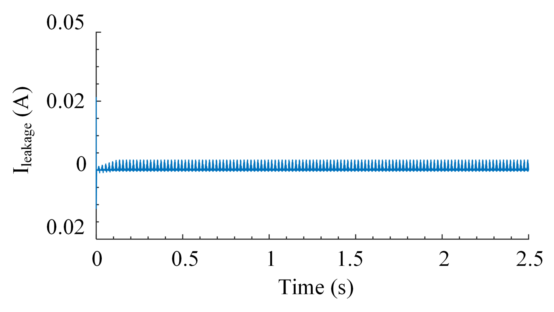
  • The influence of EMI and harmonic distortion is reduced when leakage current is kept under the standard limit;
  • Lower power ranges with higher efficiency;
  • Protection against shoot-through issues.
In this case, this article proposes the Buck-Boost Single-stage Microinverter (BBSM) topology to convert DC power to AC, which satisfies all of the aforementioned requirements. The PV system under consideration uses an appropriate switching approach that allows the inverter to run in Discontinuous Conducting Mode (DCM) and track maximum power using the Perturbation and Observation ( P & O ) technique [15]. For the first time, this paper describes a number of unique and scientific additions to the BIPV system:
  • With fewer active and passive components, buck-boost capability has been realized.
  • In the lower power range, a better efficiency was achieved.
  • Leakage current value has been reduced within the limit.
The following is an overview of the paper’s structure: Principle of operation and analysis of the proposed topology is presented in the next section. Design of passive and active elements of BBSM topology is shown in Section 3. This is followed by a loss analysis in Section 4. In 
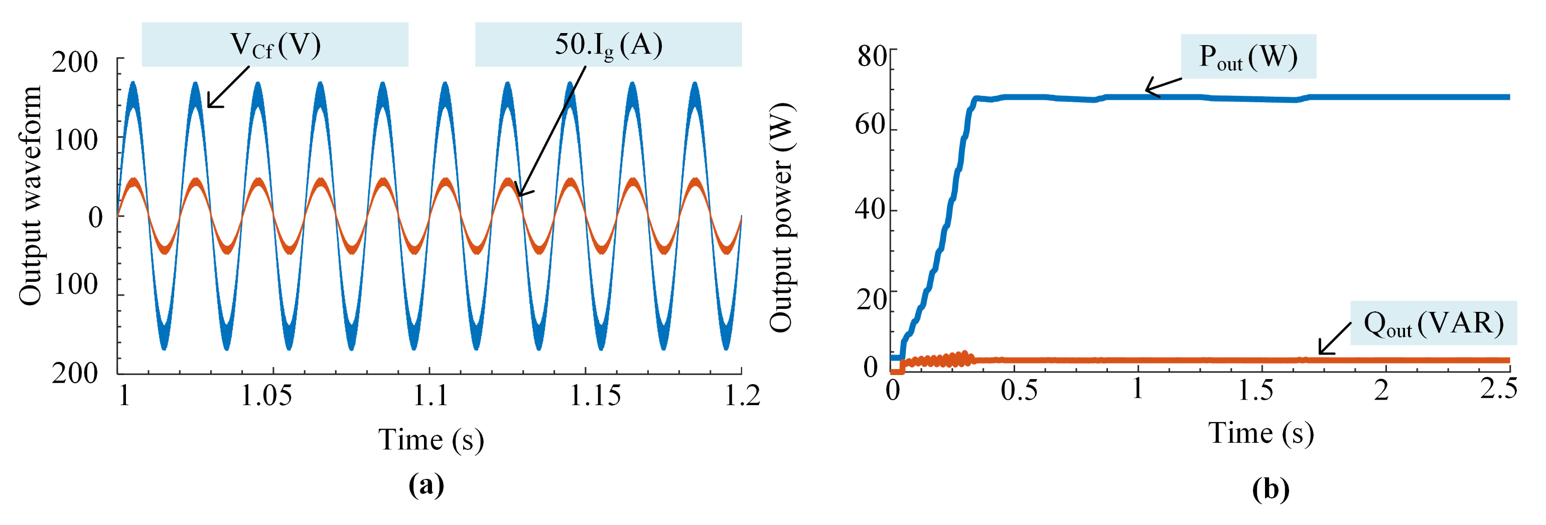
Section 5, design validation of the topology is shown using simulation and experimental results. Finally, conclusions are presented in Section 6.

2. BBSM’s Operating Principles and Analysis

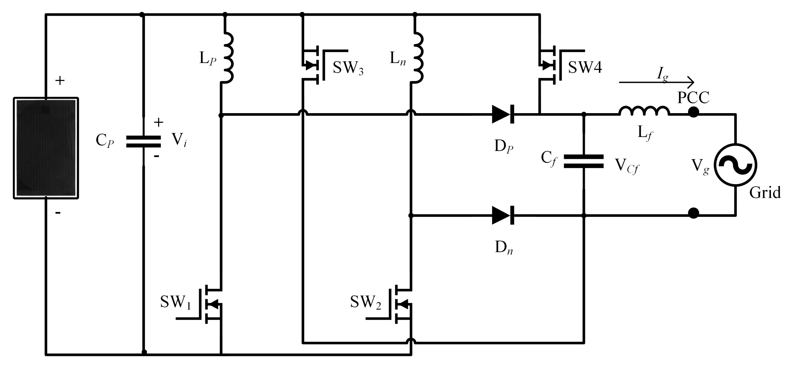
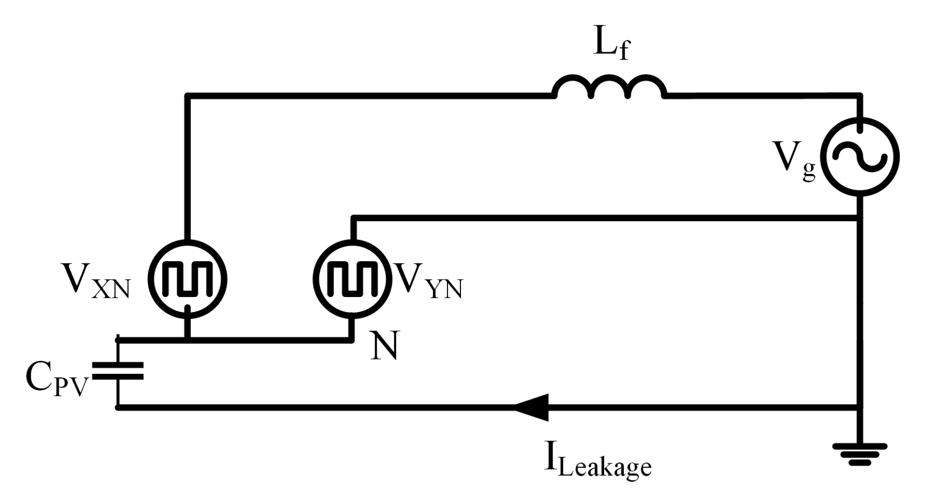
The BBSM topology is shown in 
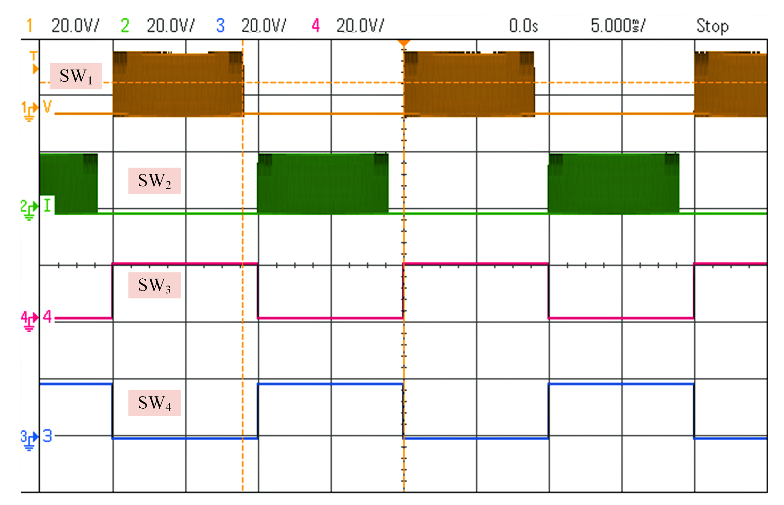
Figure 1 it encompasses four semiconductor switches controlled devices, two uncontrolled devices (diodes), and a C-type filter. At the Point of Common Coupling, the proposed inverter intersects the grid (PCC). were employed for buck-boost operation and grid injection of PV energy. They also prevent inverter shoot-through issues. This increases system reliability while also making switching processes easier. During both half cycles of the reference, S W 1 and S W 2 are activated to energize the inductors L P and L N , respectively. The S W 3 , as well as S W 4 plays a crucial role in inductors’ discharge and energy injection into the grid. The load is assumed as pure resistive load R L .
The S W 1 and S W 2 switches have a high operating frequency. The S W 3 and S W 4 switches operates at low frequency. All of the switches have a built-in safety diode. The inverter can be operated in six distinct modes, three of these modes occurred during each half cycle of the common reference or control signal. These occurred in a row, i.e., one after the other. In both reference cycles, the BBSM topology operates similarly to a typical DC-DC buck-boost converter, except that the suggested inverter topology modulates on a quasi-sinusoidal duty-cycle.
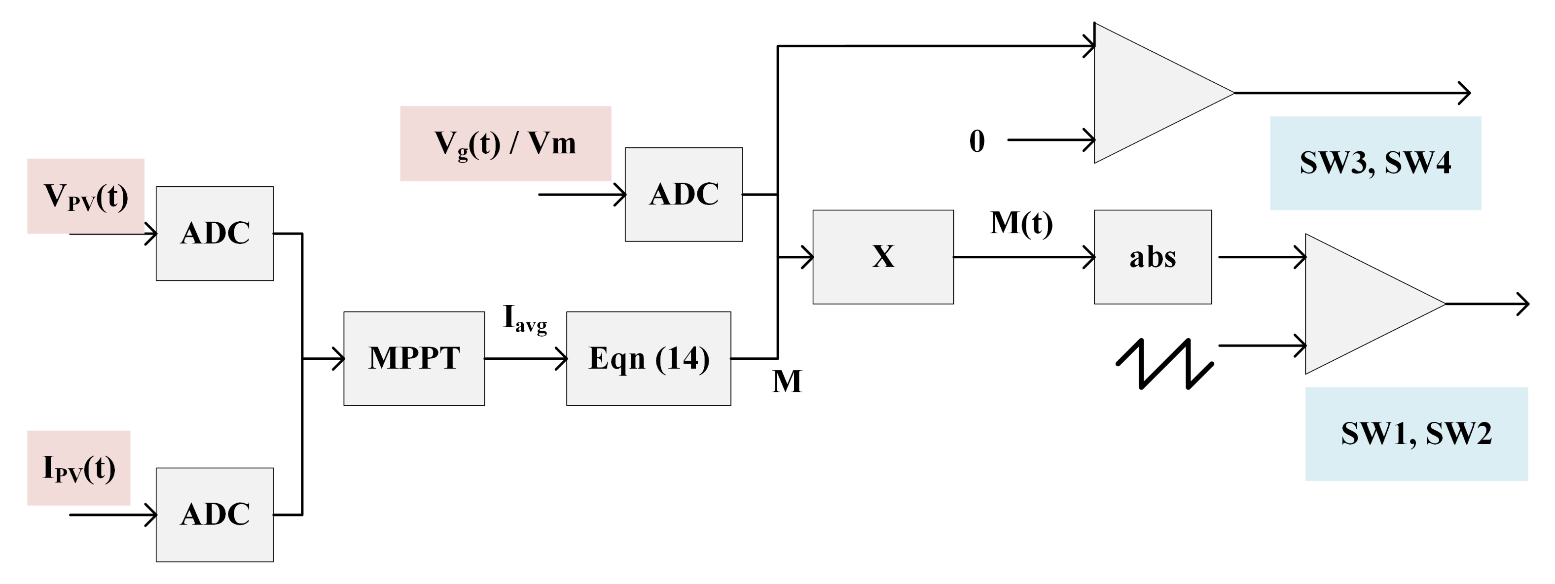
The control strategy is essentially accomplished through a two-steps scheme: the first is achieved via the control of the PV array’s voltage by the inductors’ current imposition, the second is achieved via the control of the grid current via the output capacitor’s voltage imposition. The principle of operations is described with the aid of the control variables are as follows:
  • Parameter O indicates the status of the output voltage half-cycle, during the positive part of the reference, O == 1, and switches S W 1 and S W 3 are in the ON state. During the negative part of the reference O == 0, and S W 2 and S W 4 are in the ON state. The reference cycle is obtained when V r e f is compared to 0.
  • Parameter U indicated when the output voltage V C f has to be increased U == 1, this is achieved through triggering switches S W 3 or S W 4 or to be stepped-down (decreased) then U == 0 and achieved when triggering switches S W 1 or S W 2 this is accomplished by comparing V r e f and V C f .
  • Parameter C P and C N indicates the charging / discharging process of L P and L N , respectively, as follows: C P = 1 & C N = 1, turn on S W 1 / S W 2   C P = 0 & C N = 1, turn on S W 2 )/ S W 3 this is generated by comparing the I r e f and inductor current I L .
Table 2 summarises the state of passive and active components in each mode of operation.
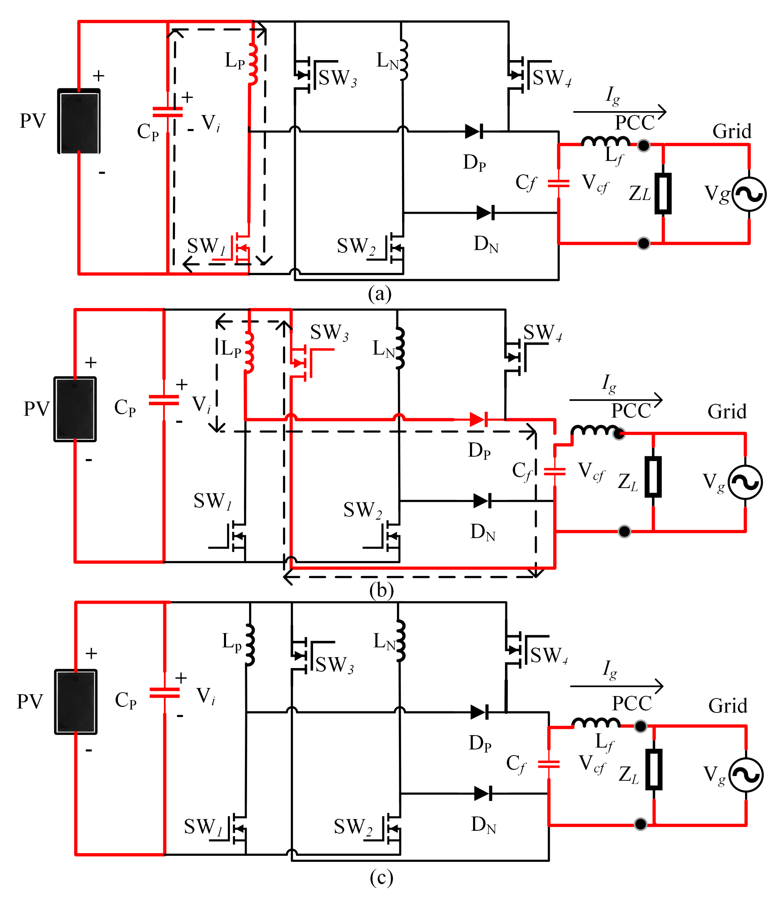
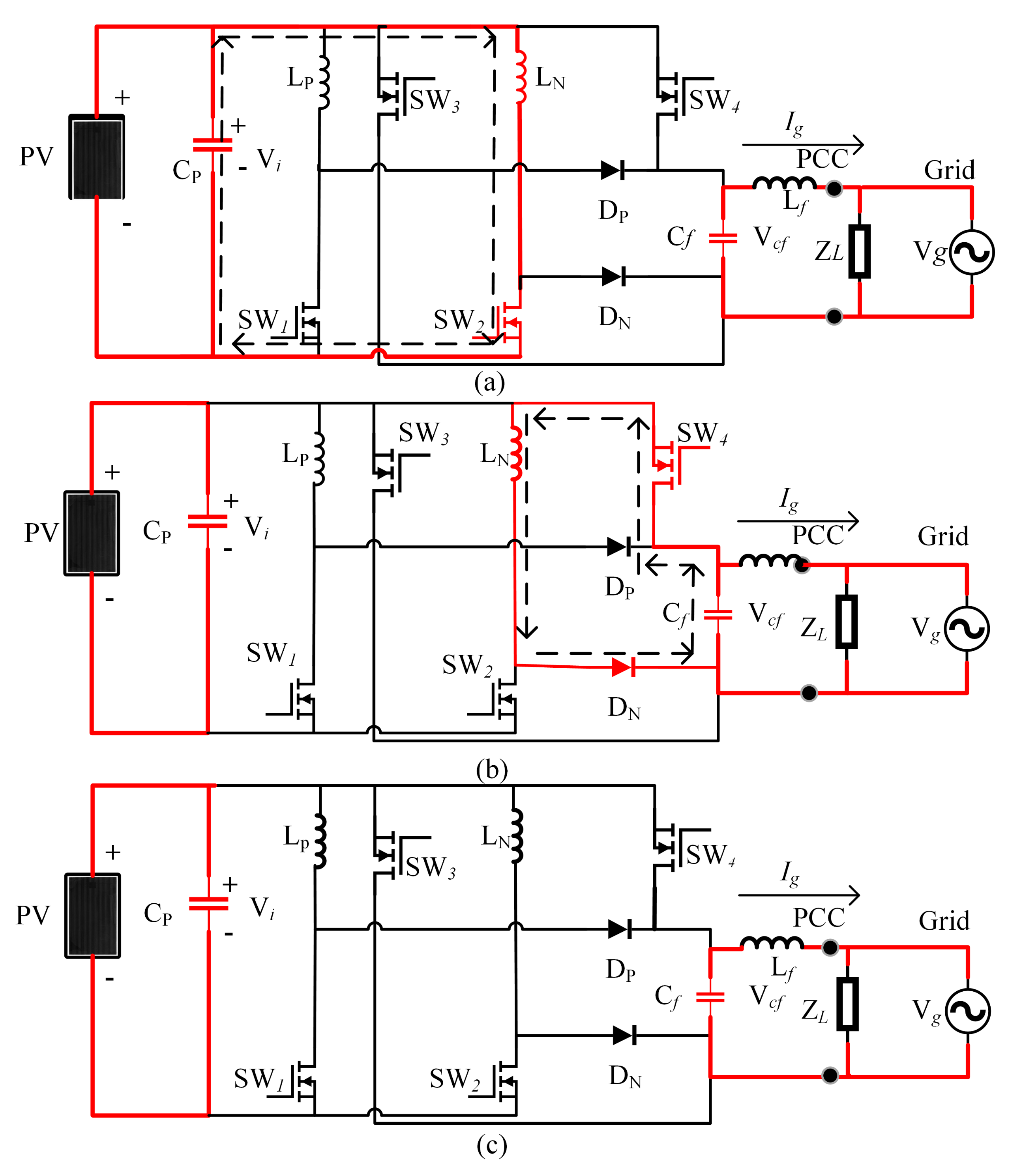
 Figure 2 and Figure 3 depicts the three modes of functioning of the topology in the positive and negative half-cycles, respectively. In different modes, the highlighted components are active. It’s vital to remember that during each operation, only one switch is in the conduction path, even if another switch is on. This may help to lower the total power loss of the system.
The operating mode P 1 is carried out for the current assessment of the inductor L P as shown in Figure 2a, and switch S W 1 is activated due to this reason. Differential equations for control variables are derived from Figure 2a. Here V i is the input voltage and V g is the grid voltage, C f is the output filter capacitor, and R L is the load.
d i L P ( t ) d t = V i L P
d v C f ( t ) d t = v g ( t ) C f R L
After storing the energy in L P during P 1 mode to provide the required voltage gain, the P 2 working mode is initiated. The stored energy is transferred through the output filter capacitor–load combination, while the positive half cycle diode D P becomes forward biased in addition to creating a closed-loop via S W 3 as well as the inductor L P , meanwhile, S W 1 is turned into its off status. The operating operation can be expressed using the differential equations from Figure 2b as follows;
d i L P ( t ) d t = v C f ( t ) L P
d v C f ( t ) d t = i L P ( t ) C f v g ( t ) C f R L
When the energy stored in inductor ( L P ) is transmitted to capacitor load combination ( C f ), the P 3 mode is then initiated. As shown in Figure 2c, the output energy of the filter capacitor is delivered under this mode.
d v C f ( t ) d t = v g ( t ) C f R L
The N 1 operation mode is employed to apply current to inductor L N , as shown in Figure 3a, and switch S W 2 is enabled for this reason. The following differential equations for control variables are derived from Figure 3a.
d i L N ( t ) d t = V i L N
d v C f ( t ) d t = v g ( t ) C f R L
After storing sufficient energy in the negative half cycle inductor ( L N ) to provide the required voltage gain, the N 2 working mode is activated. The stored energy is delivered to the filter capacitor-load combination, while the diode D N becomes forward biased in addition, establishes a path of conduction via S W 4 as well as the inductor L N , S W 2 is triggered off mean. From Figure 3b, the following differential equations are found.
d i L N ( t ) d t = v C f ( t ) L N
d v C f ( t ) d t = i L N ( t ) C f v g ( t ) C f R L
N 3 mode is activated, when all of the energy from the inductor ( L N ) is shifted to the capacitor ( C f ). As shown in Figure 3c, the filter capacitor energy can be delivered to the output load in this mode.
d v C f ( t ) d t = v g ( t ) C f R L
The current flow direction is represented as dashed lines in Figure 2 and Figure 3.
To evaluate the proposed topology, the following assumptions are made.
  • Equation (11) shows the relationship between F g (Grid frequency) and F s w (Switching frequency of switches S W 1 and S W 2 ).
    F S W = 2 n × F g n N
  • The semiconductor devices device possesses ideal characteristics.
  • Throughout each switching time-period T S W , the grid voltage v g ( t ) is considered constant.
  • MOSFETs and diodes have zero forward resistance and infinite reverse resistance.
  • The duty cycle remains constant during each switching period.
  • The inverter’s operation is maintained DCM.
  • The load is resistive
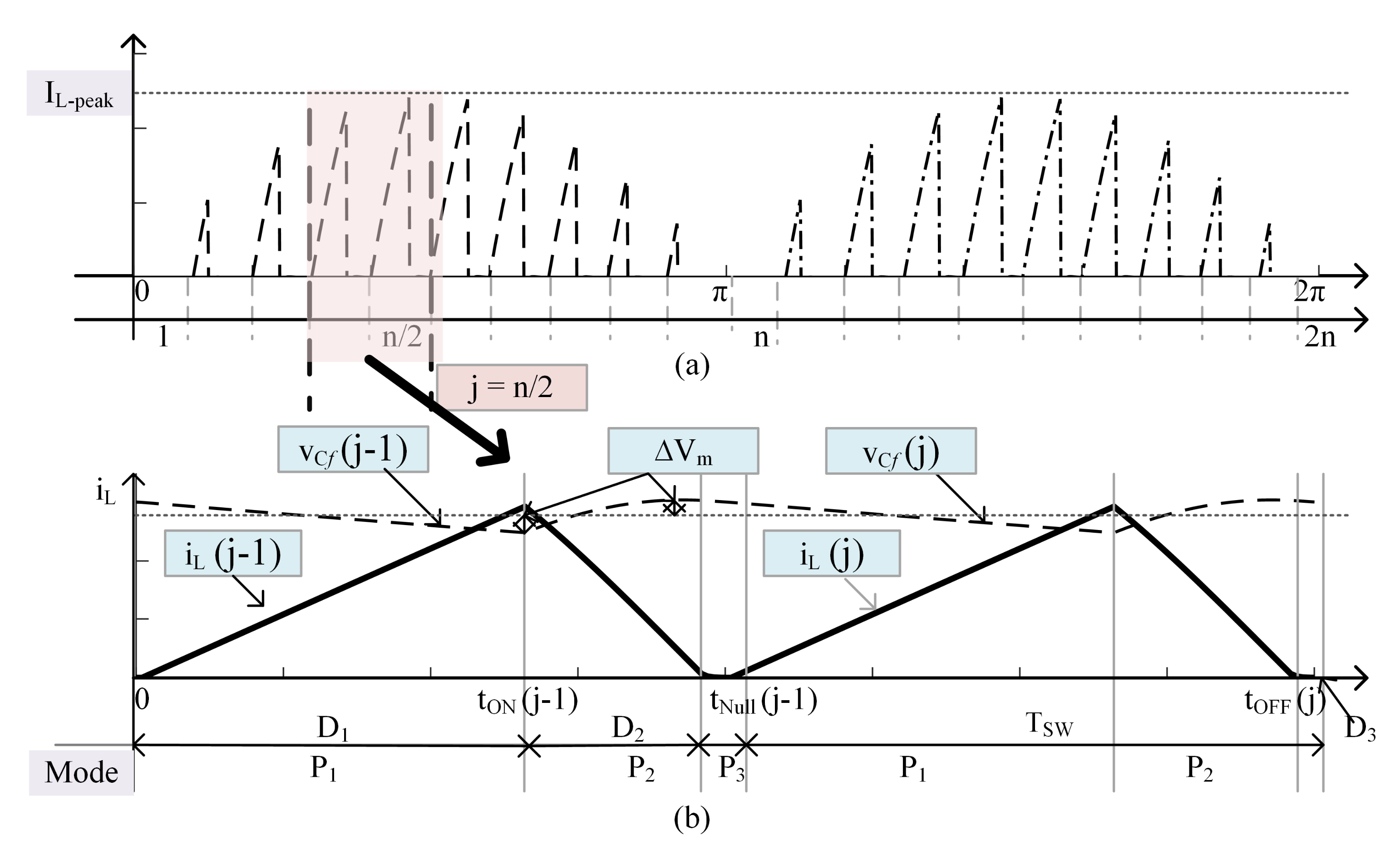
 R L
The L P and L N behave similarly during both reference cycles, they are referred to as L in the analytical section. Inductor current at the peak interval in zoomed in Figure 4b. In P 1 mode, the inductor current increases. For the jth switching period, the inductor charging current I L achieves its maximum value at t = t O N ( j ) . As the quantity of energy transferred to the output is determined by the magnetizing current of the inductor, the peak value of the current ( i L P e a k ) is provided in (12) and depends on the output power. (13) can be used to express the energy stored in the inductor ( E i n ).
i L p e a k ( j ) = V i L D 1 ( j ) T S W
e i n ( j ) = 1 2 L i L p e a k ( j ) 2
Using Equation (13), the average value of current in inductor I a v g throughout a swapping period expressed in Equation (14). As noted in (15), the current at output A is a sinusoidal changing current and that can be expressed as I g , as illustrated in the expression (14). As a result, the energy required on the output side E o u t can be written as (16). The peak output voltage is V m in this case. By equating the Formulas (13) and (16), the charging duty ratio may be stated as (17).
i a v g ( j ) = L i L p e a k ( j ) 2 2 V i T S W
i g ( j ) = i a v g ( j ) s i n ( ω t )
e o u t ( j ) = i a v g ( j ) V m s i n 2 ( π n j ) T S W
D 1 ( j ) = 2 L i a v g V m V i 2 T S W s i n ( π n j )
The discharging duty ratio can be determined as (19).
V i L D 1 ( j ) T S W V C f L D 2 ( j ) T S W = 0
D 2 ( j ) = 2 L i a v g ( j ) V m T S W
The inverter modulation index is thus indicated by (20) and static gain is given in (21).
M = 2 L I a v g V m V i 2 T S W
V m V i = D 2 L R L T S W

2.1. DCM Operational Requirement

The inductor current discharge completely in time D 2 T S W , if the average value of the current is lesser than the maximum ripple. Until the next switching cycle, the current will stay zero. When this pattern occurs, the inverter is in DCM mode. If the suggested inverter topology meets DCM condition for the time duration j = n / 2 , it operates in DCM mode throughout the grid cycle. The essential requirement for sampling duration j = n / 2 of the grid voltage is applied as described in (22) for calculating the peak modulation index M limit for maintaining DCM functioning. In accordance with the conditions, the peak modulation index limit is calculated based on (23).
D 1 ( n / 2 ) T S W + D 2 ( n / 2 ) T S W = T S W
M m a x = 1 V i V m + 1
The peak output voltage, V m , is used here.

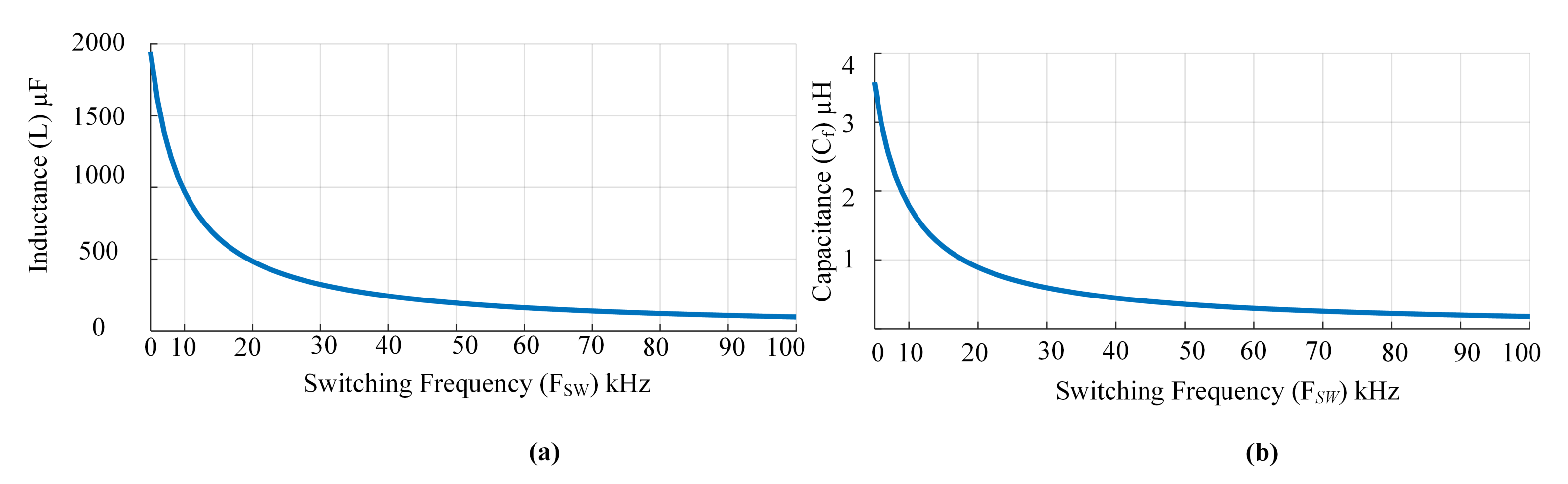
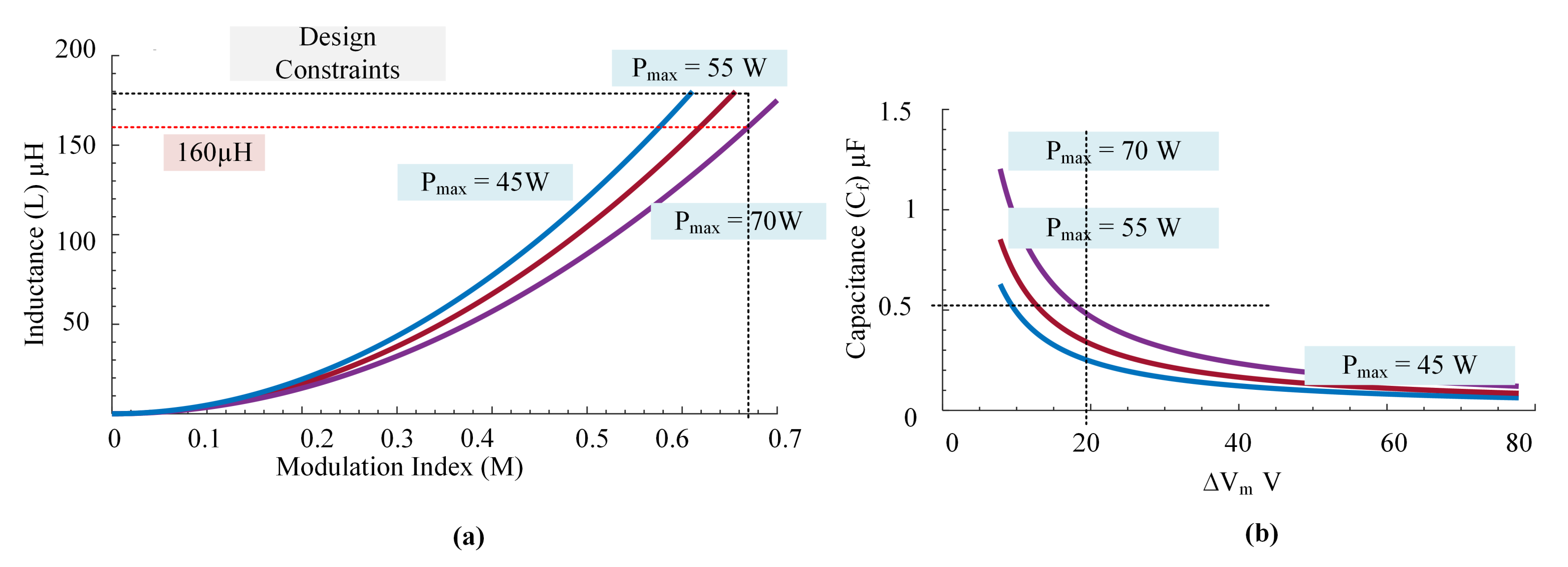
2.2. Elements for Energy Storage Design

As the physical size of the inverter is determined by the size of its energy storage devices, the design of these elements is critical. 
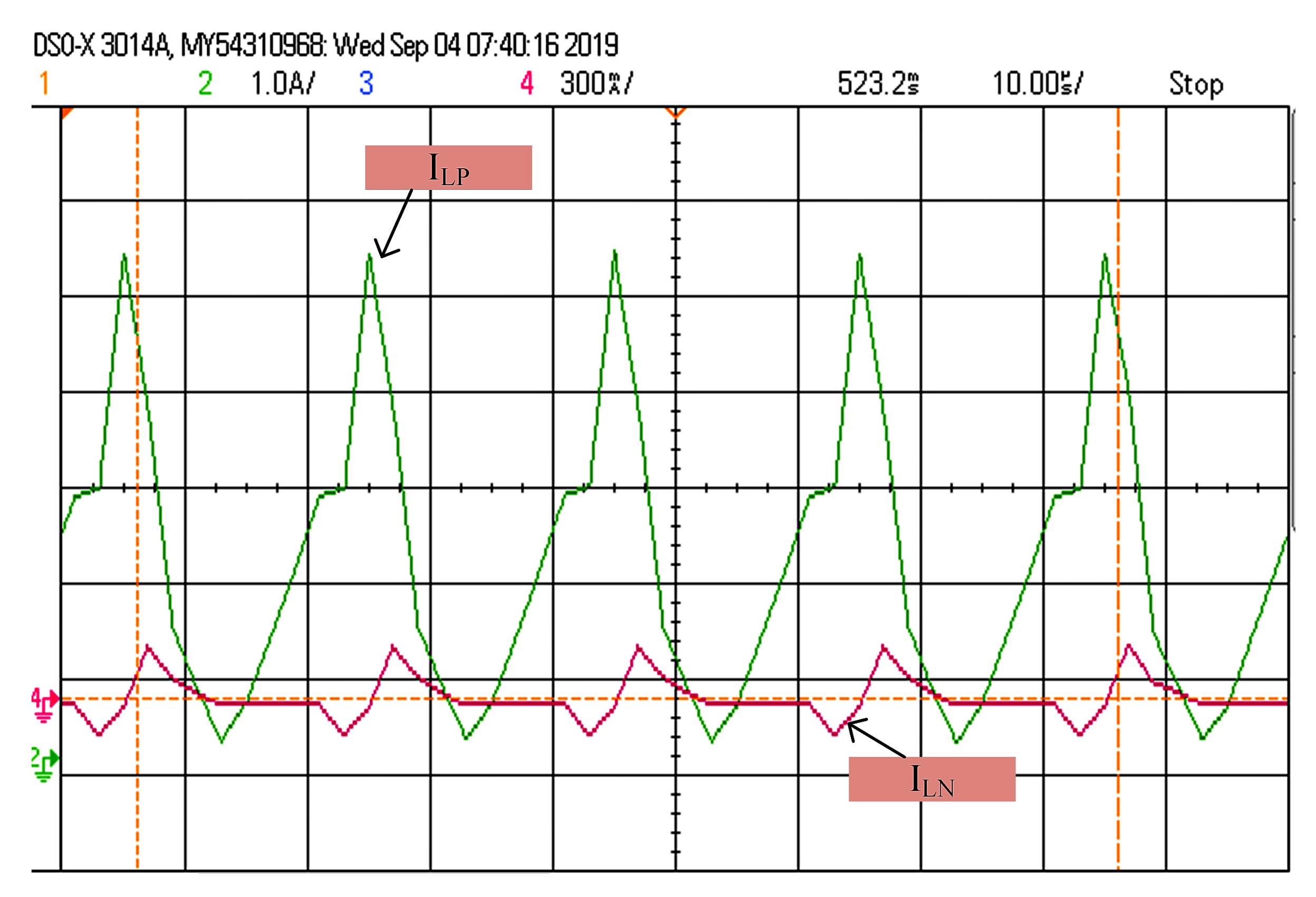
Figure 4 depicts the inductor current i L ( t ) . Energy is delivered in a discrete form since the inverter works in DCM. During each switching interval ( T S W ) Inductor L will store and transmits energy. Thus, a C f capacitor is used in the inverter topology. The inductor’s energy has been completely transferred to the capacitor Cf. During the peak phase ( j = n / 2 ), it transfers most of the energy from L to C f . The inductor should be able to handle ( 2 P m a x ), where P m a x is the maximum input power. This situation assures when the grid receives ( P m a x ) during each grid cycle, hence (24) is derived from (13). Equation (25) may be used to calculate the inductor value by replacing (12) into (24). The relationship between L and F S W is seen in Figure 5a from (
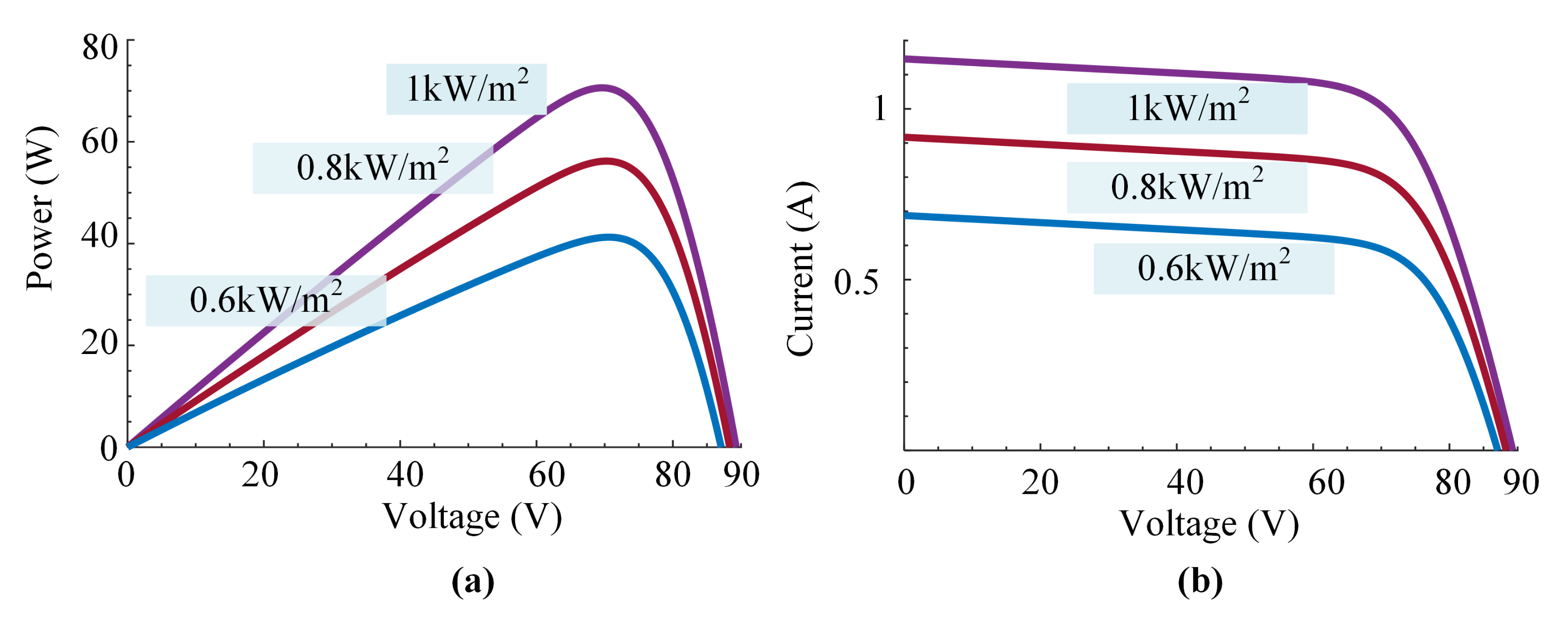
25). The maximum power output of a Photo-Voltaic module determines the design value of L. This condition ensures that DCM will work at any power level.
1 2 L I L P e a k ( n / 2 ) 2 = 2 P m a x T S W
L = V i 2 t O N 2 ( n / 2 ) 4 P m a x T S W L V i 2 M m a x 2 T S W 4 P m a x
The total energy accumulated within the inductor (L) during D 1 is totally released to the capacitor during D 2 , as shown in Figure 4. The variations in the energy over D 2 can be represented in (26). The C f is designed based on the expression (27). The relationship between F S w and C f is depicted in Figure 5b from (27)
2 P m a x T S W = C f [ ( V m + V m ) 2 ( V m V m ) 2 ] 2
C f = P m a x T S W V m V m

2.3. Power Device Selection

The whole cost and performance of a system are affected by the rating of the power devices in an inverter, which includes storage duration, current gain, and switching frequency. the calculation of voltage, as well as current load on power equipment, can be calculated. Switches maximum voltage is the same as the capacitor’s maximum voltage. Similarly, the peak current of the switches matches the maximum inductor current. The total active switch stress SS must be computed if the inverter has k switching devices as stated in (28) using the RMS current I R M S i and the voltage V i . Table 3 lists all of the switches RMS current as well as the peak voltage expressions.
S S = i = 1 k V i I R M S

3. BBSM Topology Design

The passive elements design relation was derived from the analysis of the BBSM topology, while designing, the nominal power of the inverter is considered equal to the maximum power of the PV module. Thin-film PV modules are widely employed in BIPV applications, according to [16]. For the purpose of inverter validation, we have looked at the first solar PV module. V g = 110 V, P m a x = 70 W, F g = 50 Hz, V i = 73 V. On the basis of Figure 5, the optimal switching frequency of 50 kHz was chosen, resulting in 2n = 1000. For these specifications, the maximum modulation index is derived using (23) as M m a x = 0.68 . The peak permissible inductance for the discontinuous mode of operation (DCM) is estimated using (25) as L 177 μ H . Black dotted line in Figure 6a shows the two constraints L 177 μ H and M m a x = 0.68 for the determination of the inductance value. It can be shown that these two constraints are satisfied when the inductance value is 160 μ H . The filter capacitor value C f for output voltage is plotted in Figure 6b based on (27). The capacitance value is between 0.4 μ F and 0.5 μ F for a peak ripple of 10 % . Thus, in this project 0.47 μ F capacitor is chosen. The DC-link capacitor C P is determined as 220 μ F for this project [13].

4. Loss Analysis

Using the elements design value the expected losses of the BBSM topology is discussed in this section. The power loss analysis includes core loss, conduction loss and switching loss evaluation.

4.1. Core Loss

Changing magnetic flux fields causes core loss within a material. The core loss density ( P L ) is a function of B , and f S W , where ( B ) is half of the flux swing as shown in (29). In order to approximate the constants core loss charts are utilised.
P L = a B 2 b f S W c
Here flux swing B is given in (30).
B = N I L a v g μ 0 l g
I L a v g = I L p e a k k = 1 n s i n ( π n k ) n
Number of turns (N). The ripple current in the inductor is △ I L , and the air gap in the magnetic core is l g . The permeability of the air gap is μ 0 , which is 4 π × 10 7 . As a result, the equation for P c o r e is (32)
P c o r e = P L l e A e
The magnetic core’s mean path length is l e , and the cross-sectional area is A e .

4.2. Conduction Loss

The total conduction loss is equal to the summation of the inductor loss and conduction loss in power devices.
The inductor conduction loss P c o n d L can be calculated using the average inductor current as well as the inductor’s series resistance R L from the (33).
P c o n d L = I L a v g 2 R L
In the BBSM, the switch S W 3 , as well as switch S W 4 , operates in a symmetrical way for both half cycles, resulting in the same conduction losses, as determined by (34).
P c o n d S W 3 , 4 = I R M S S W 3 , 4 2 R d s
The conductive loss of a diode is estimated as (36) using the power loss accompanied with the fixed voltage drop ( V F V ) as well as the resistance R a k .
P c o n d D P , N = I R M S D P , N 2 R a k + I R M S D P , N V F V
Here, the I R M S D P , N is given in Table 3, R a k and V F V are determined from the datasheet of the diode.

4.3. Switching Loss

The switching loss of S W 3 and S W 4 switches is negligible since they operate at a low switching frequency. Similarly, because the inverter works in DCM, the diode’s switching loss owing to reverse recovery is zero. Due to the DCM operation, turn on losses are nil in switches S W 1 and S W 2 . As a result, the inverter’s total switching losses are indicated in (36).
P S W 1 , 2 = < V s w > T < I s w > T 2 f s w t f + E O F F f s w
The switch’s Turn OFF energy loss E O F F as well as fall time t f may be found in the datasheet. The inverter’s losses are estimated using the parameters reported in Table 4. The BBSM inverter’s power loss is documented in Table 5. All topologies losses are computed using a 70 W system.

5. Design Validation

In order to validate the proposed BBSM topology a simulation and experimental test has been conducted as given below.

5.1. Simulation Results

The simulation using MATLAB / Simulink is carried out for the proposed microinverter and the ratings, as well as component values are displayed in Table 6. A thin film Photovoltaics module FS 270 which is of 70 W is considered, with the approaches given in [17,18] are being used to simulate it for simulation. Figure 7a,b show the I-V and P-V graphs generated from the model for 1 kW/m 2 , 0.8 kW/m 2 and 0.6 kW/m 2 , respectively. The testing control circuit and the block diagram of the inverter is given in (20) and plotted in Figure 8, respectively. In this project, the Perturbation and Observation ( P & O ) approach suggested in [19] is employed for MPPT by sampling I P V and V P V . At a maximum power of 70 W, Figure 9a,b show the current flow through the inductors L P and L N , respectively. The theoretical calculations of the peak current through the inductor I L P e a k and M m a x for the DCM functioning of the BBSM inverter topology is convincingly validated. At the maximum power rating, the inverter’s output voltage and current are 110 V and 0.636 A, respectively, as shown in Figure 10a. The active power P and reactive power Q in the grid are plotted in Figure 10b.
Further research of the suggested inverter’s open-loop control was conducted by changing the degree of irradiation level. The MPPT operation is shown in Figure 11a while adjusting the level of irradiation ( 0.8 kW / m 2 to 1 kW / m 2 ) in 1.25 s. Despite the fact that it functions in the MPP field, further research in this area is essential for exact operation. During irradiation change, Figure 11b and Figure 12a,b show alterations in output current, output power, and input voltage, respectively. The results show that the inverter is operating correctly when the irradiation changes.
To evaluate the flow of leakage current in the proposed inverter, a parasitic capacitance of 70 nF was used in the simulation [20]. According to German regulations DIN VDE 0126-1-1, if the leakage current exceeds 300 mA (RMS), the inverter must be removed from the grid. As shown in Figure 13, a circuit for resonance condition is created for the transformerless inverter. PV parasitic capacitance ( C P V ) as well as filter inductor ( L f ) are included in the resonant circuit. X, and Y are the inverter’s terminals, which are coupled to the single-phase grid via L f . As shown in Figure 13, the inverter maybe simplified into an equivalent circuit consisting of V X N and V Y N . As a result, leakage current is determined by V X N as well as V Y N . (37) can be used to define the Common Mode Voltage (CMV). The leakage current travels via the parasite capacitance and to the grid when there is a V C M differential. As demonstrated in Figure 14, the proposed topology has low-frequency components V X N and V Y N . As the voltage differential between the BIPV module’s ground and the grid is low-frequency, the parasitic capacitance’s equivalent impedance is high. This high impedance, as seen in Figure 15, restricts the flow of leakage current I L e a k a g e . In this simulation, a parasitic capacitance of 70 nF was employed to check the I L e a k a g e [20]. The proposed inverter’s leakage current is negligibly tiny, as shown in Figure 15.
V C M = V X N + V Y N 2

5.2. Experimental Results

Based on the specifications in Table 6, an experimental model of a 70 W, 110 V, 50 Hz inverter was designed. In Figure 16a, the experimental settings in the laboratory are shown, and in Figure 16b, the proposed BBSM topology is shown. In the experimental research, the chroma programmable DC power supply 62150H-600S solar array simulator was utilized to simulate the identical simulated Photovoltaic module characteristics. For loading, the programmable AC/DC electronic load 63802 was employed. A chroma 3-phase programmable AC source 61704 was used to duplicate the grid. The switching strategy was created in MATLAB in addition it is linked to the dSPACE-1104 control desk in the control area. All waveforms were captured using a DSOX3014 oscilloscope.
Figure 17 shows the switching pulses created by the dSPACE-1104 by using the TLP350 gate driver. As mentioned in the theory, S W 1 as well as S W 2 , represent 50 kHz pulses, while S W 3 and S W 4 represent pulses at 50 Hz. Currents through L P and L N with a magnified view during P m a x = 70 W are shown in Figure 18. It clearly validates the inverter’s DCM functioning and I L P e a k of around 6 A during P m a x = 70 W, as described in the theoretical analysis. Figure 19 shows the output voltage and current in relation to the input voltage and current at steady state. The output voltage and current RMS values are the same around the values analyzed and simulated. From Figure 19 the efficiency is obtained is 96.4% as given in (38). As expected from the theoretical analysis efficiency is above 95%.
E f f i c i e n c y ( % ) = ( 109.84 × 0.6116 ) 71.8 × 0.97 × 100 = 96.4
The waveforms of real power, phase angle, reactive power, current, voltage, power factor, and apparent power during P m a x = 70 W are shown in Figure 20. It is evident that the power factor is approximately 1. The injected current from the inverter’s Total Harmonic Distortion (THD) and Fast Fourier Transform (FFT) values are shown in Figure 21. The THD value of the current fed to the grid is around 5%. The input current, voltage, and steady-state output at 0.8 kW/m 2 are shown in Figure 22, along with the efficiency calculation. Various input voltages inverter efficiency curve is shown in Figure 23. Voltage across and current through the MOSFETS and Diodes are shown in Figure 24 and Figure 25 respectively. The various values of efficiency from the proposed topology in low to nominal power operation is determined using a DC power supply in addition to a resistive load. Table 7 tabulates the comparison between simulation and experimental results, it clearly shows that due to the use of real time elements efficiency during experimental test is slightly lower.

5.3. Comparison of Topologies

The BBSM uses fewer switches in the conduction path, according to a comparison of other microinverters in Table 8. Other topologies efficiency were determined using the same criteria used in this study. The BBSM topology is more efficient and has less passive elements than other topologies, making it excellent for BIPV applications. Furthermore, the proposed inverter has a negligible leakage current. When compared to other microinverters, BBSM is more efficient and reliable due to the employment of an appropriate number of components in the conduction channel.

6. Conclusions

A buck-boost single-stage microinverter (BBSM) with fewer number of elements, with high efficiency and reliability were proposed in this paper. Due to the limited number of components, a higher performance is achieved. Design details of all the elements were derived in the paper. MATLAB/Simulink simulation and experimental setup was used to verify the design technique of the inverter systems. The results of the BBSM topology shows that it had negligently low leakage current with buck-boost performance, high operational efficiency, THD level for the injected current is within the limit, and prevented shoot-through. According to a comparison examination of the proposed inverter with similar topologies it shows that proposed topology can be recommended topology for Building Integrated PV system.

Author Contributions

Conceptualization, D.M.; methodology, D.M.; software, D.M.; validation, D.M. and R.C.N.; formal analysis, D.M., M.E.F. and R.K.M.; investigation, D.M., A.S. and P.S.; resources, D.M.; data curation, D.M. and R.C.N.; writing—original draft preparation, D.M., R.C.N. and M.E.F.; writing—review and editing, D.M., R.C.N. and M.E.F.; visualization, D.M. All authors have read and agreed to the published version of the manuscript.

Funding

This research received no external funding.

Institutional Review Board Statement

Not applicable.

Informed Consent Statement

Not applicable.

Data Availability Statement

Not applicable.

Conflicts of Interest

The authors declare no conflict of interest.

References

  1. Li, G.; Xuan, Q.; Akram, M.; Akhlaghi, Y.G.; Liu, H.; Shittu, S. Building integrated solar concentrating systems: A review. Appl. Energy 2020, 260, 114288. [Google Scholar] [CrossRef]
  2. Mousa, O.B.; Kara, S.; Taylor, R.A. Comparative energy and greenhouse gas assessment of industrial rooftop-integrated PV and solar thermal collectors. Appl. Energy 2019, 241, 113–123. [Google Scholar] [CrossRef]
  3. Bastidas-Rodriguez, J.D.; Franco, E.; Petrone, G.; Ramos-Paja, C.A.; Spagnuolo, G. Maximum power point tracking architectures for photovoltaic systems in mismatching conditions: A review. IET Power Electron. 2014, 7, 1396–1413. [Google Scholar] [CrossRef]
  4. Zare, M.H.; Mohamadian, M.; Beiranvand, R. Single-stage AC module with series power decoupling capability for connecting PV to a single-phase power grid. IET Power Electron. 2016, 10, 517–524. [Google Scholar] [CrossRef]
  5. Chander, A.H.; Kumar, L. MIC for reliable and efficient harvesting of solar energy. IET Power Electron. 2018, 12, 267–275. [Google Scholar] [CrossRef]
  6. Ahmad, A.A.; Abrishamifar, A.; Samadi, S. Low-frequency current ripple reduction in front-end boost converter with single-phase inverter load. IET Power Electron. 2012, 5, 1676–1683. [Google Scholar] [CrossRef]
  7. Hu, Y.; Du, Y.; Xiao, W.; Finney, S.; Cao, W. DC-link voltage control strategy for reducing capacitance and total harmonic distortion in single-phase grid-connected photovoltaic inverters. IET Power Electron. 2015, 8, 1386–1393. [Google Scholar] [CrossRef]
  8. Mathew, D.; Naidu, R.C. Investigation of single-stage transformerless buck–boost microinverters. IET Power Electron. 2020, 13, 1487–1499. [Google Scholar] [CrossRef]
  9. Jha, K.; Mishra, S.; Joshi, A. High-quality sine wave generation using a differential boost inverter at higher operating frequency. IEEE Trans. Ind. Appl. 2014, 51, 373–384. [Google Scholar] [CrossRef]
  10. Wang, C.M.; Chen, T.J. Novel single-stage half-bridge series-resonant buck-boost inverter. IEEE Trans. Aerosp. Electron. Syst. 2004, 40, 1262–1270. [Google Scholar] [CrossRef]
  11. Gao, M.; Chen, M.; Zhang, C.; Qian, Z. Analysis and implementation of an improved flyback inverter for photovoltaic AC module applications. IEEE Trans. Power Electron. 2013, 29, 3428–3444. [Google Scholar] [CrossRef]
  12. Azary, M.T.; Sabahi, M.; Babaei, E.; Meinagh, F.A.A. Modified single-phase single-stage grid-tied flying inductor inverter with MPPT and suppressed leakage current. IEEE Trans. Ind. Electron. 2017, 65, 221–231. [Google Scholar] [CrossRef]
  13. Jain, S.; Agarwal, V. A single-stage grid connected inverter topology for solar PV systems with maximum power point tracking. IEEE Trans. Power Electron. 2007, 22, 1928–1940. [Google Scholar] [CrossRef] [Green Version]
  14. Ardashir, J.F.; Sabahi, M.; Hosseini, S.H.; Blaabjerg, F.; Babaei, E.; Gharehpetian, G.B. A single-phase transformerless inverter with charge pump circuit concept for grid-tied PV applications. IEEE Trans. Ind. Electron. 2016, 64, 5403–5415. [Google Scholar] [CrossRef]
  15. Mathew, D.; Chinnappa Naidu, R.; Wang, Y.; Busawon, K. Single-stage microinverter with current sensorless control for BIPV system. IET Renew. Power Gener. 2021, 15, 2468–2479. [Google Scholar] [CrossRef]
  16. Tsai, C.Y.; Tsai, C.Y. See-through, light-through, and color modules for large-area tandem amorphous/microcrystalline silicon thin-film solar modules: Technology development and practical considerations for building-integrated photovoltaic applications. Renew. Energy 2020, 145, 2637–2646. [Google Scholar] [CrossRef]
  17. Derick, M.; Rani, C.; Rajesh, M.; Farrag, M.; Wang, Y.; Busawon, K. An improved optimization technique for estimation of solar photovoltaic parameters. Sol. Energy 2017, 157, 116–124. [Google Scholar] [CrossRef]
  18. Mathew, D.; Rani, C.; Kumar, M.R.; Wang, Y.; Binns, R.; Busawon, K. Wind-driven optimization technique for estimation of solar photovoltaic parameters. IEEE J. Photovolt. 2017, 8, 248–256. [Google Scholar] [CrossRef]
  19. Esram, T.; Chapman, P.L. Comparison of photovoltaic array maximum power point tracking techniques. IEEE Trans. Energy Convers. 2007, 22, 439–449. [Google Scholar] [CrossRef] [Green Version]
  20. Melo, F.C.; Garcia, L.S.; de Freitas, L.C.; Coelho, E.A.; Farias, V.J.; de Freitas, L.C. Proposal of a photovoltaic AC-module with a single-stage transformerless grid-connected boost microinverter. IEEE Trans. Ind. Electron. 2017, 65, 2289–2301. [Google Scholar] [CrossRef]
  21. Kumar, A.; Sensarma, P. A four-switch single-stage single-phase buck–boost inverter. IEEE Trans. Power Electron. 2016, 32, 5282–5292. [Google Scholar] [CrossRef]
  22. Gautam, V.; Sensarma, P. Design of Ćuk-derived transformerless common-grounded PV microinverter in CCM. IEEE Trans. Ind. Electron. 2017, 64, 6245–6254. [Google Scholar] [CrossRef]
  23. Rajeev, M.; Agarwal, V. Analysis and Control of a Novel Transformer-Less Microinverter for PV-Grid Interface. IEEE J. Photovolt. 2018, 8, 1110–1118. [Google Scholar] [CrossRef]
  24. Roy, J.; Xia, Y.; Ayyanar, R. High Step-Up Transformerless Inverter for AC Module Applications With Active Power Decoupling. IEEE Trans. Ind. Electron. 2018, 66, 3891–3901. [Google Scholar] [CrossRef]
Figure 1. Buck-Boost Single-stage Microinverter.
Energies 14 07854 g001
Figure 2. (a) Circuits that are equivalent to Mode P 1 . (b) Circuits that are equivalent to Mode P 1 . (c) Circuits that are equivalent to Mode P 1 .
Energies 14 07854 g002
Figure 3. (a) Circuits that are equivalent to Mode N 1 . (b) Circuits that are equivalent to Mode N 2 . (c) Circuits that are equivalent to Mode N 3 .
Energies 14 07854 g003
Figure 4. (a) Inductor current ( I L ), (b) Inductor current and capacitor voltage during the peak switching interval.
Energies 14 07854 g004
Figure 5. (a)The relationship between the switching frequency ( F S W ) and the inductance value. (b) The relationship between the switching frequency ( F S W ) and the capacitance value.
Energies 14 07854 g005
Figure 6. (a) Inductance value vs. modulation index. (b) V m versus capacitance value for various power ratings.
Energies 14 07854 g006
Figure 7. (a) PV voltage index versus Power. (b) PV voltage versus current for different irradiation level.
Energies 14 07854 g007
Figure 8. Block diagram of the control technique used for BBSM.
Energies 14 07854 g008
Figure 9. (a) Current through inductor L P . (b) Current through inductor L N .
Energies 14 07854 g009
Figure 10. (a) Injected current and output voltage. (b) Active and reactive power at the output side.
Energies 14 07854 g010
Figure 11. (a) P V curve of MPPT. (b) Changes in active and reactive power under irradiation.
Energies 14 07854 g011
Figure 12. (a) Variation in the output current I g . (b) Variation in input voltage V i with respect to changes in irradiation levels.
Energies 14 07854 g012
Figure 13. BBSM equivalent circuit to show path for leakage current.
Energies 14 07854 g013
Figure 14. Common mode voltage V X N .
Energies 14 07854 g014
Figure 15. Leakage current at P m a x = 70 W.
Energies 14 07854 g015
Figure 16. (a) Setup for the experiment. (b) Power circuit of BBSM.
Energies 14 07854 g016
Figure 17. Switching pulses at P m a x = 70 W.
Energies 14 07854 g017
Figure 18. Inductor currents I L P and I L N during P m a x = 70 W.
Energies 14 07854 g018
Figure 19. Steady-state output and input voltage and current waveforms during P m a x = 70 W.
Energies 14 07854 g019
Figure 20. Power quality measurements during P m a x = 70 W.
Energies 14 07854 g020
Figure 21. THD of injected current at P m a x = 70 W.
Energies 14 07854 g021
Figure 22. Input and output voltage and current with efficiency at 800 W/m 2 .
Energies 14 07854 g022
Figure 23. Efficiency curve of the proposed inverter.
Energies 14 07854 g023
Figure 24. Voltage across and current through the MOSFET.
Energies 14 07854 g024
Figure 25. Voltage across and current through the Diode.
Energies 14 07854 g025
Table 1. Ratings of microinverters available in market [5].
MicroinverterMaximum Power (W) η (%)Weight (kg)
ABB Micro-0.25-I-OUTD25096.53.5
SMA SB240-US-9925095.92.9
LS250-AU25096.32
Darfon MIG300260952.5
INVOLAR MAC250250952.9
SBT-250WF25094.32
SUNCON SC-MAC250A23595.22.44
RSMI-250L25095.5NA
Table 2. Components operational status at each mode.
Passive ElementsActive ElementsMode
O C P ( C n ) U S W 1 ( S W 2 ) S W 3 ( S W 4 ) D P ( D n )
11 (0)01 (0)1 (0)RB (RB) P 1
10 (0)10 (0)1 (0)FB (RB) P 2
10 (0)00 (0)1 (0)RB (RB) P 3
00 (1)00 (1)0(1)RB (RB) N 1
00 (1)10 (0)0 (1)RB (FB) N 2
00 (0)00 (0)0 (1)RB (RB) N 3
RB = Reverse bias, FB = Forward bias
Table 3. Current and voltage expressions.
QuantityRelation
I R M S S W 1 , S W 2 V i T S W 3 L M 3 π
I R M S S W 3 , S W 4 T S W 2 L V i 2 M 3 6 V m
V D p , V D n , V S W 3 , V S W 4 V m
V S W 1 , V S W 2 V i + V m
Table 4. Power loss calculating parameters.
Number of turns N74
Air gap in the magnetic core l g 2 mm
Inductor resistance R L 6.75 m Ω
Permeability of air gap μ o 4 π × 10 7
ON state resistance of Diode R a k 0.03 Ω
Mean path length of magnetic core l e 171.1 mm
Turn OFF energy loss E O F F 0.015 mWs
Falling time t f 4.5 ns
Cross sectional area A e 49 mm 2
Fixed voltage drop V F V 1.5 V
ON state resistance of MOSFET R d s 0.43 Ω
Table 5. The Power loss of the BBSM inverter.
Losses
SW Conduction losses2.44
SW Switching losses5.18 × 10 3
D Conduction losses0.72
Inductor core loss0.89
Inductor copper loss0.52
Table 6. Element values obtained from the design [5].
Input Parameters I m a x = 0.96 A, V m a x = 73 V
Output Parameters I R M S = 0.63 A, V R M S = 110 V, P m a x = 70 W
Switching DevicesDiode—FEP30JP-4
MOSFET—FQP10N20C
Gate driver—TLP350
Capacitor C P = 220 μ F ,
C f = 0.47 μ F , M P X 2250 V A C , Film capacitor
Inductor ( L P , L N ) R D C = 14 m Ω , 160 μ H , I L P e a k = 6.2 A
Table 7. Comparison of results obtained using simulation and experimental study.
Simulation ResultsExperimental Results
I L P e a k 6 A5.6 A
Efficiency9896.4
Output voltage ( V g R M S )110 V109.84 V
Output Current ( I g R M S )0.624 A0.614 A
THD2.83%4.09%
Table 8. Comparison of different topologies [5].
[14][21][22][20][12][23][24]BBSM
2017201720172017201820182019
Number of switches44545674
Number of switches22322341
in conduction
Number of capacitor32211231
voltage stress>>>>>>>>
of switches V m V m V m V m V m V m V m
Number of diode62040232
Number of inductor23232242
Shoot through problemYesNoNoNoNoNoYesNo
Leakage current (mA)≈22.7≈0≈0≈22.9≈0≈0NA≈0
Efficiency (%)93.493.694.292.490.278993.896.4
Publisher’s Note: MDPI stays neutral with regard to jurisdictional claims in published maps and institutional affiliations.

