Abstract
This paper demonstrates that in the Phase-Shifted Full-Bridge (PSFB) buck-derived converter, there is a random delay associated with the blanking time produced by the leakage inductance. This random delay predicts the additional phase drop that is present in the frequency response of the open-loop audio-susceptibility transfer function when the converter shows a significant blanking time. The existing models of the PSFB converter do not contemplate the delay and gain differences associated to voltage drop produced in the leakage inductor of the transformer. The small-signal model proposed in this paper is based on the combination of two types of analysis: the first analysis consists of obtaining a small-signal model using the average modeling technique and the second analysis consists of studying the natural response of the power converter. The dynamic modeling of the Phase-Shifted Full-Bridge converter, including the random delay, has been validated by simulations and experimental test.
1. Introduction
In recent years, the Phase-Shifted Full-Bridge (PSFB) converter has been widely used in several applications such as renewable energy power systems [1,2], energy storage systems for electric vehicles [3,4,5], railway applications [6], server power supply unit [7], telecom power supplies or data centers [8,9], etc.
On the other hand, there is a strong tendency to increase the switching frequency in order to achieve higher power density, and thus, reduce the volume of the switched mode power supplies SMPS [10,11,12,13]. Increasing the switching frequency of the converter leads to an increase the switching losses of the MOSFET. Furthermore, problems with electromagnetic interference, EMI, can be generated. For this reason, it is common to opt for topologies that could implement some of the soft-switching techniques, such as Zero-Voltage-Switching (ZVS). In the PSFB converter, the primary switches stress is reduced when the ZVS condition is achieved. Additionally, the ZVS improves the reliability of the converter [14,15].
The ZVS operation is achieved when the energy stored in the leakage inductance of the transformer is able to discharge the output capacitor, , before the MOSFET is turned on [15]. Therefore, the ZVS avoids the overlap of the drain current and the drain-source voltage in order to reduce switching losses. For this reason, the design of the leakage inductance is very important in the PSFB converter. On the other hand, this leakage inductance creates a blanking time interval, which depends on the operating point of the converter. The blanking time is not a controllable quantity. Currently, many published works can be found that deal with the design considerations to improve the static behavior of the PSFB converter [15,16,17,18,19]. However, there is a limited number of references that perform a detailed analysis of its dynamic behavior.
A small-signal model of the PSFB converter based on the buck converter approximation is presented in [15,20], which is a good estimation for cases where the blanking time interval is small and the output filter inductance, , is much higher than the transformer leakage inductance referred to the secondary, . The small-signal model of the PSFB converter presented in [21,22,23,24,25,26] is based on the three-terminal PWM switch model [27]. Although the PWM switch modeling method is a simple way for modeling PWM converters, the small-signal models of the PSFB converter obtained in [21,22,23,24,25,26] are a derivation of the model presented in [15,20].
On the other hand, there are cases in which the leakage inductance is not able to store the necessary energy to discharge the output capacitors of the MOSFETs, as occurs when the converter is operating with light load. For this reason, in order to extend the range of the ZVS, it is necessary to add an extra inductor in series to the transformer leakage inductor. When the equivalent inductance (leakage inductance plus additional inductance) has a considerable value with respect to the output filter inductance, a change in the output filter inductor current slope occurs during the blanking time. Additionally, the blanking time interval can be noticeably increased even with light load. On the other hand, the blanking time also depends on the load current, so increasing the load current also increases the blanking time interval. The small-signal models based on the approximation of the buck converter could not be accurate, since there is an inherent delay associated to the blanking time. When the blanking time interval increases, the delay starts to be noticed in certain transfer functions, such as audio-susceptibility. This delay can be measured experimentally, and it is discussed in detail in Section 3.
Another small-signal model of the PSFB converter is presented in [28]. This model is based on a discrete-time modeling of the current waveforms. This approach is conceptually very accurate, especially in the high frequency range, but it would become complex and not very versatile model, since the number of state variables increases dramatically, when external elements such as input filter or/and output post-filter are added to the converter. Additionally, the explicit transfer functions of the converter are not shown.
Therefore, this paper proposes a new small-signal model of the PSFB converter, based on an average model, which considers the additional switching stages due to the leakage inductance. In addition, this model includes a delay term associated with the blanking time produced by the leakage inductance.
The small-signal model proposed in this paper is based on the combination of two types of analysis: the first analysis consists of obtaining an averaged model of the PSFB converter. This averaged model is then linearized and perturbed in order to obtain the characteristic coefficients of the injected-absorbed-current method (IAC) [29,30]. The IAC method was chosen to obtain the proposed model of the PSFB converter, since this method provides an analytical solution and allows the calculation of transfer functions, such as audio-susceptibility, input impedance and output impedance in a more convenient way. The characteristic coefficients allow to see the physical effects that each of the perturbations (input voltage, output voltage and control quantity) produce on the currents of the input and output ports of the converter. The second analysis consists of studying the natural response of the power converter and this paper demonstrate that there is an inherent delay due to the blanking time interval. This random delay predicts the additional phase drop that is present in the frequency response of the open-loop audio-susceptibility transfer function when the converter shows a significant blanking time. This random delay has not been considered in previous works.
Since the proposed model is based on an averaging process, it only predicts accurately the dynamic behavior up to half the switching frequency. However, in most cases, in order to design the compensator, this model is accurate enough.
The converter transfer functions and impedances have been validated by simulation and experimentally.
The original contribution of this paper is a new small-signal model of the PSFB converter. This model has two main advantages:
- -
- The model predicts more accurately the gain of the transfer function because the additional switching stage due to the leakage inductance is taken into account. This is especially important when the leakage inductance (referred to the secondary side of the transformer) is comparable to the output filter inductance.
- -
- Additionally, this new model is capable of predicting the additional phase drop that is generated in the frequency response of the open-loop audio-susceptibility transfer function when the blanking time is significant.
The paper is organized as follows. In Section 2, the characteristic coefficients of the IAC method that represent the small-signal model of the PSFB converter are obtained. In Section 3, the natural response of the power converter is analyzed in order to complete the proposed model. In Section 4, a validation by simulation has been performed. In Section 5, experimental validation of the proposed small-signal model of the PSFB converter is performed. Finally, conclusions are drawn in Section 6.
2. Small-Signal Model Based on the Average Modeling Technique
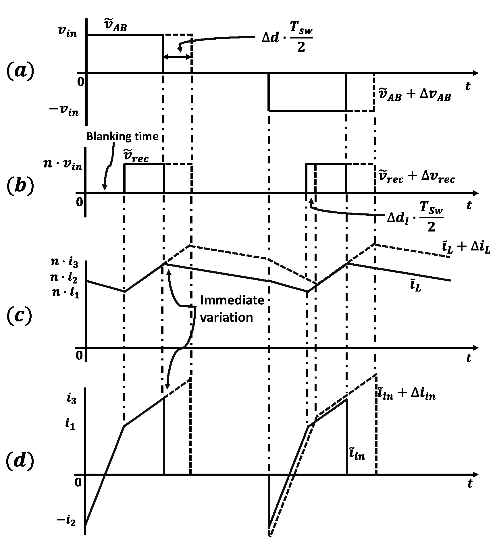
The schematic of the power converter is shown in Figure 1. The converter is operating in continuous conduction mode, CCM, and the zero-voltage-switching, ZVS, condition is achieved. The steady-state waveforms of the leakage inductor current, , output inductor current referred to primary, , voltage at terminals A-B, , and secondary voltage, , are shown in Figure 2. The blanking time interval has been exaggerated for this analysis. The duty ratio, , is determined by the phase shift, , of the gating signals between the switches of the left leg ( and the right leg (). The blanking time interval, , is caused by the leakage inductance of the transformer. This interval represents the time it takes for the leakage inductance to change the direction of the current flowing through the primary winding of the transformer. The secondary voltage, , is maintained at 0 V during this interval; therefore, there is a reduction in the duty ratio [15]. The blanking time interval depends on the operating point of the converter. During the interval and interval, the leakage inductance referred to the secondary and output inductance are in series. However, during blanking time interval, the two inductors are no longer in series, so there is a change in the output current slope that is more noticeable when the leakage inductance referred to the secondary is equal to or higher than the output inductance.
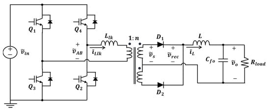
Figure 1.
Schematic of the PSFB converter.
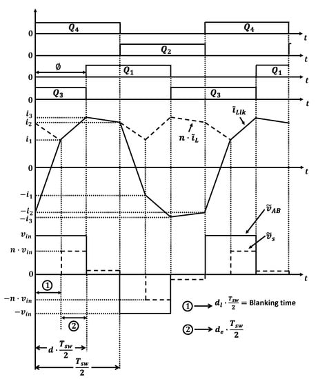
Figure 2.
PSFB steady-state waveforms (the blanking time interval has been exaggerated to highlight the effect).
The duty ratio is defined by Equation (1) [15]:
Equations (2)–(4) are the characteristic values of the leakage and output inductor current waveform:
By replacing Equations (1)–(4) into Equation (6), the rectified voltage as function of , , and is obtained:
The average output inductor current is now given by Equation (8):
Putting Equations (1)–(4) into Equation (9) and solving for , then Equation (10) is obtained. It can be seen from Equation (10) that the blanking time interval depends on the operating point conditions:
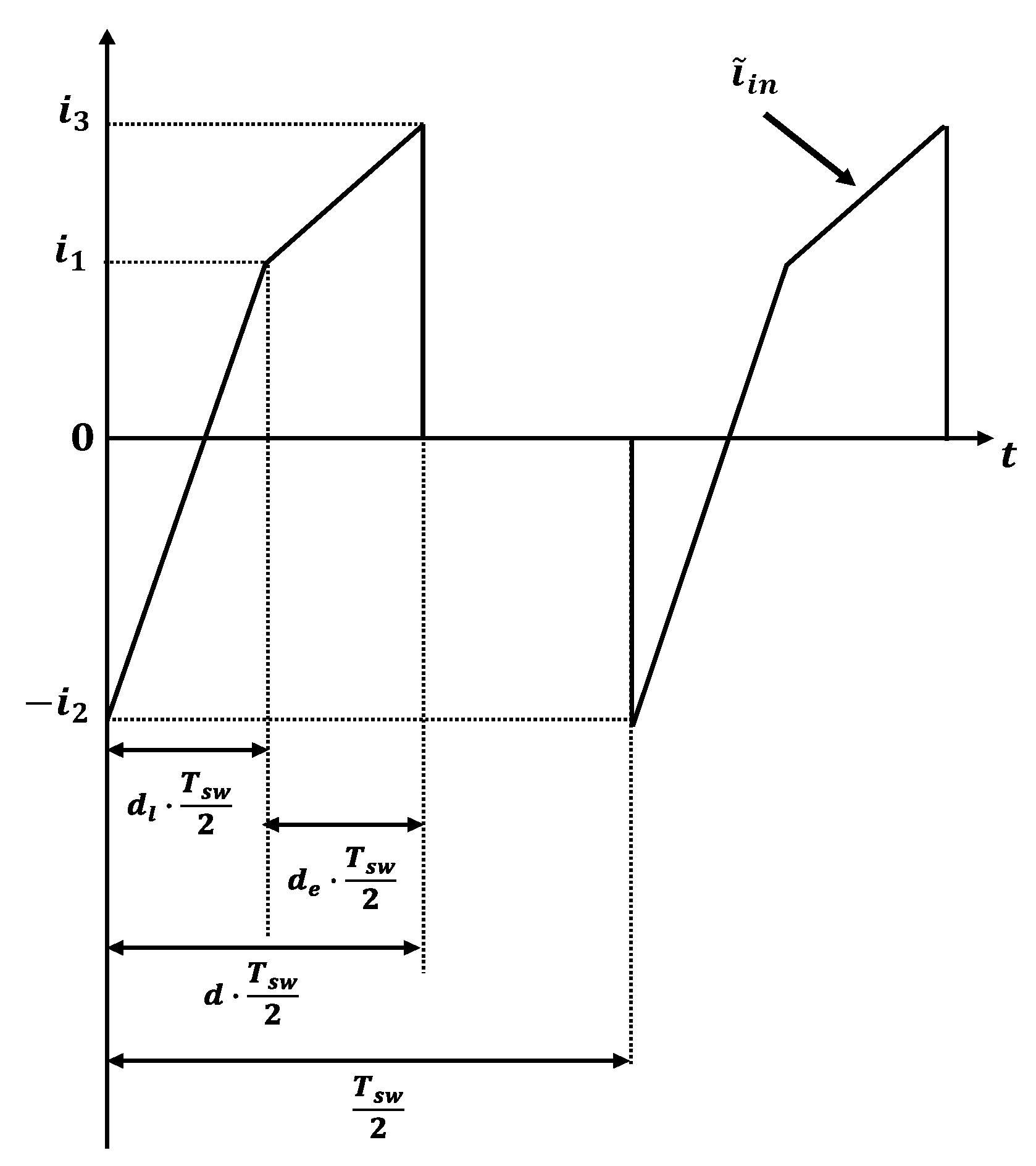
On the other hand, the waveform of the input current is shown in Figure 3, so its average value is given by Equation (11):
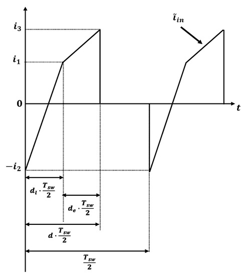
Figure 3.
Input current waveform.
The average model of the PSFB converter is shown in Figure 4.
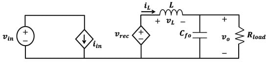
Figure 4.
Averaged model of the PSFB converter.
Replacing Equation (10) into Equation (7), the average rectified voltage as function of the duty ratio, , input voltage, , output voltage, , and output inductor current, , has been obtained. After linearizing and perturbing, then the small-signal of the output inductor voltage is obtained. The constant coefficients of Equation (14) are given in Appendix A.
From the circuit of Figure 4, Equation (15) is obtained:
Replacing Equation (15) into Equation (14), the output inductor current as function of , and is obtained:
Therefore, the characteristic coefficients of the output port are finally obtained:
Replacing Equations (2)–(4) and (10) into Equation (12), the average input current as function of the duty ratio, , input voltage, , output voltage, , and output inductor current, , has been obtained. After linearizing and perturbing, the characteristic coefficients of the input port are obtained. The constant coefficients of Equations (20)–(22) are given in Appendix A.
3. Natural Response of a PSFB Converter
It is necessary to study the natural response of the PSFB converter in order to obtain a complete small-signal model. In this section, the open-loop output inductor current response and the open-loop input current response due to a small input voltage perturbation, small output voltage perturbation and small duty ratio perturbation is analyzed.
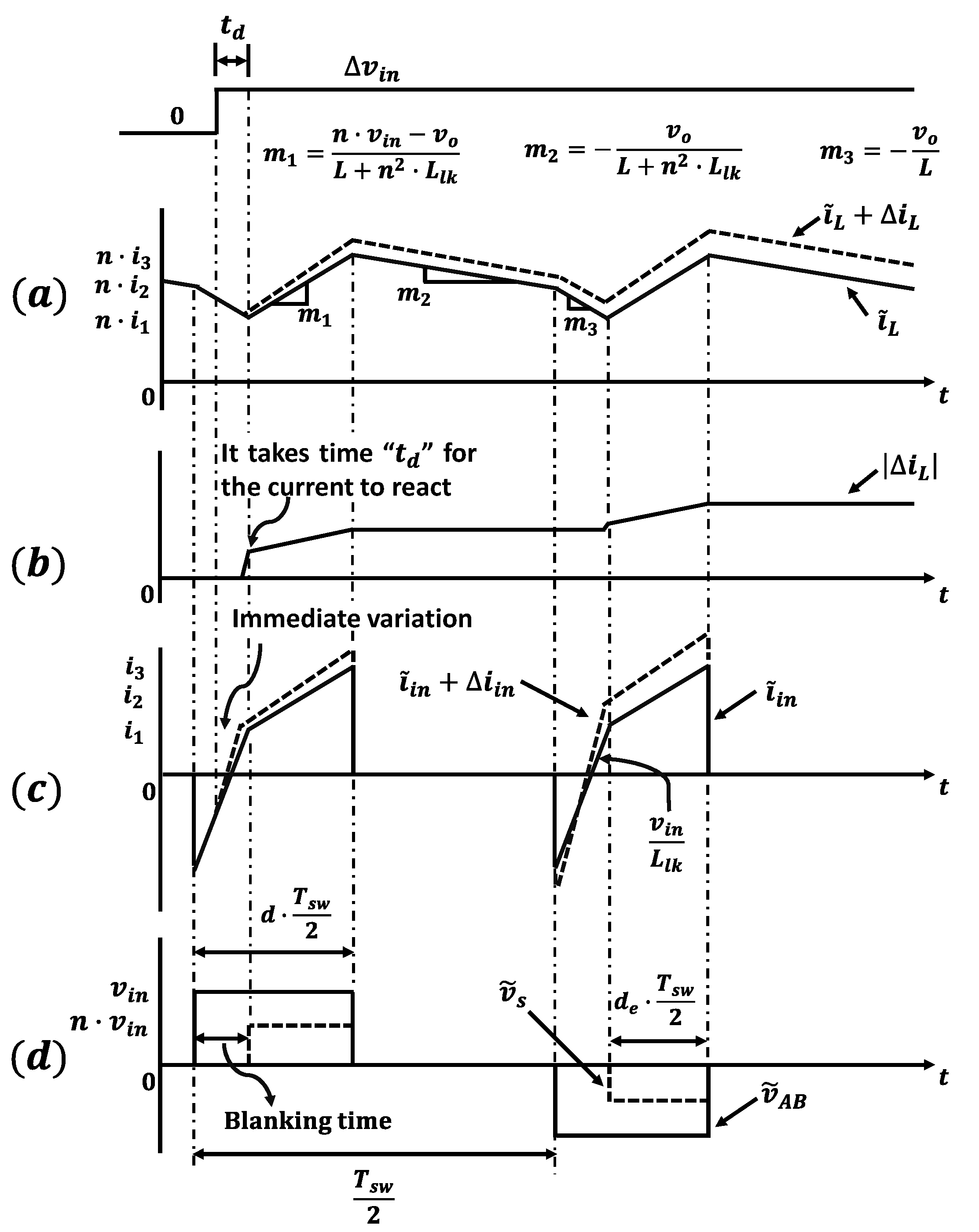
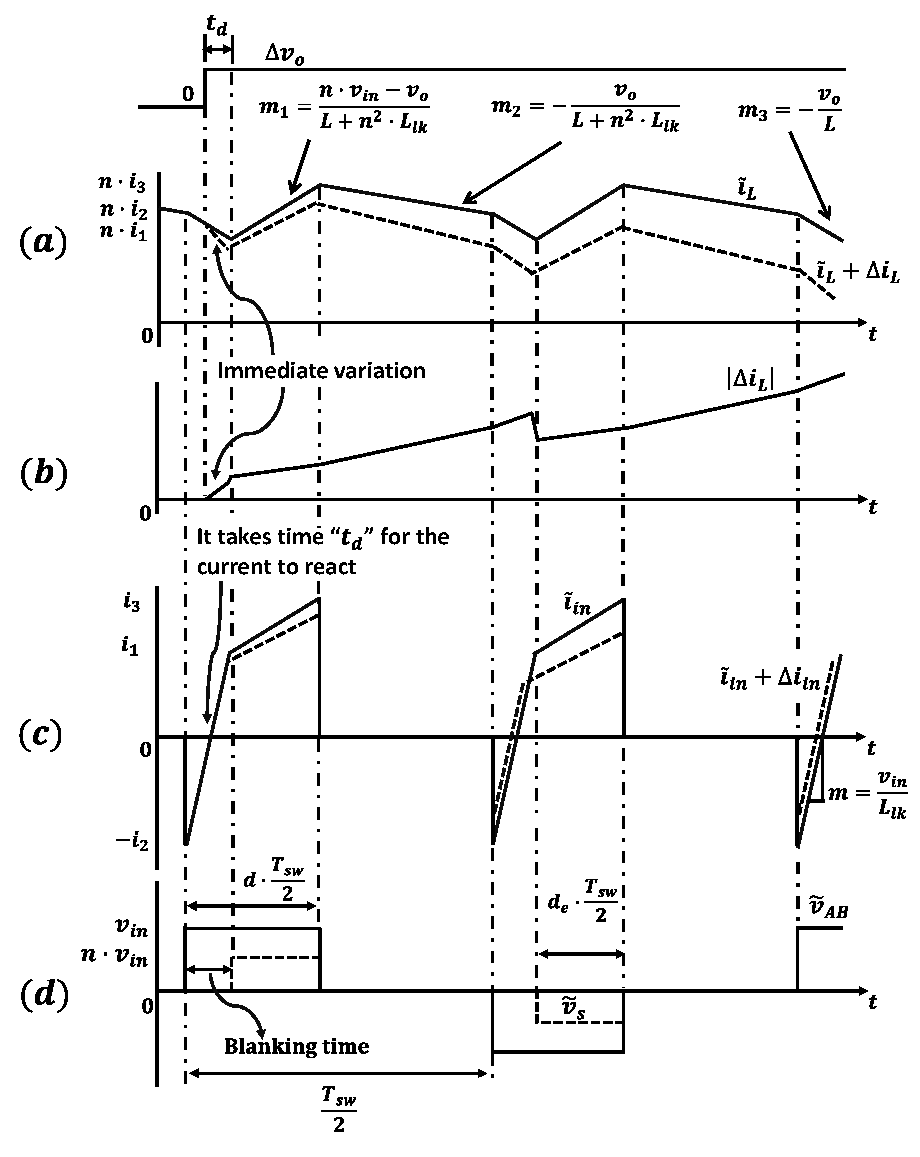
First, the output inductor current dynamic response to a small input voltage step change is analyzed. The output voltage and duty ratio are assumed to remain constant. If a small input voltage step occurs during the blanking time interval, then the output inductor current does not change immediately since the output inductor current slope, , during this interval does not depend on the input voltage as shown in Figure 5a. The term represents the difference between the instantaneous output inductor current and the operating point output inductor current. The variation of the output inductor current occurs after the blanking time interval has elapsed, as shown in Figure 5b. Therefore, there is a delay associated to the blanking time, since it depends on the moment in which the input voltage perturbation is injected until the interval begins. If the input voltage perturbation occurs in interval , the output inductor current varies immediately, since the output inductor current slope, , during this interval depends on the input voltage. Therefore, there is no delay associated with this interval. Finally, if the input voltage perturbation occurs during the interval , there is no delay, since the rectified voltage during this interval does not depend on the input voltage, and furthermore, if a constant duty ratio is considered, then this interval does not present dynamics, and something similar happens in the buck converter, since during this interval a delay in the audio-susceptibility transfer function is not associated. Later, it will be verified by simulation that the interval does not introduce a delay.
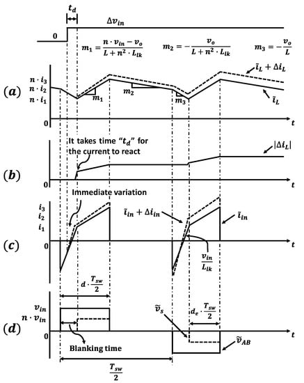
Figure 5.
Dynamic response to an input voltage step change. (a) Output inductor current, (b) incremental component of output inductor current, (c) input current and (d) primary and secondary voltage.
The input current dynamic response to a small input voltage step change is analyzed. If a small input voltage step occurs during the blanking time interval, then the input current changes immediately since the input current slope during this interval depends on the input voltage as shown in Figure 5c. If the input voltage perturbation occurs in the interval , the input current varies immediately since the input current slope during this interval depends on the input voltage. Therefore, there is no delay associated with this interval. If the input voltage perturbation occurs during the interval , there is no delay, since it has the same effect as the case of the output inductor current.
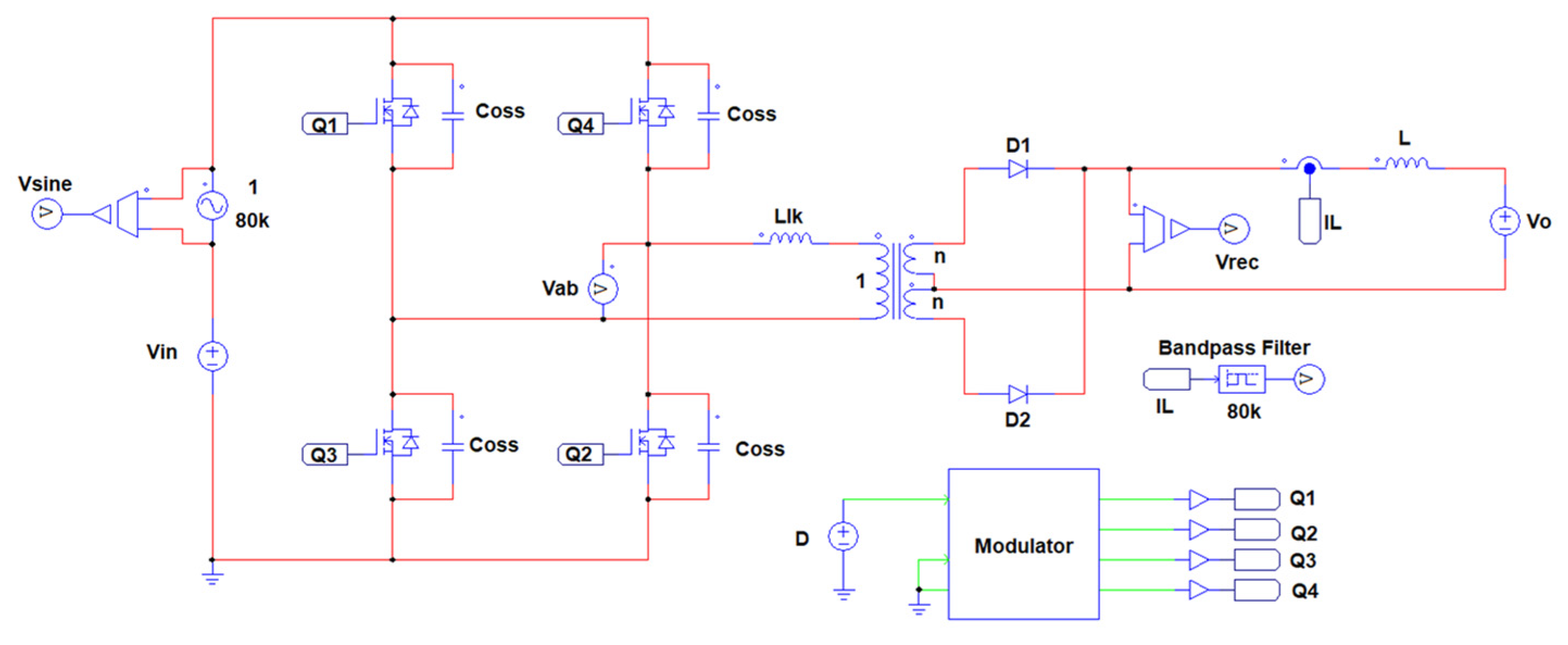
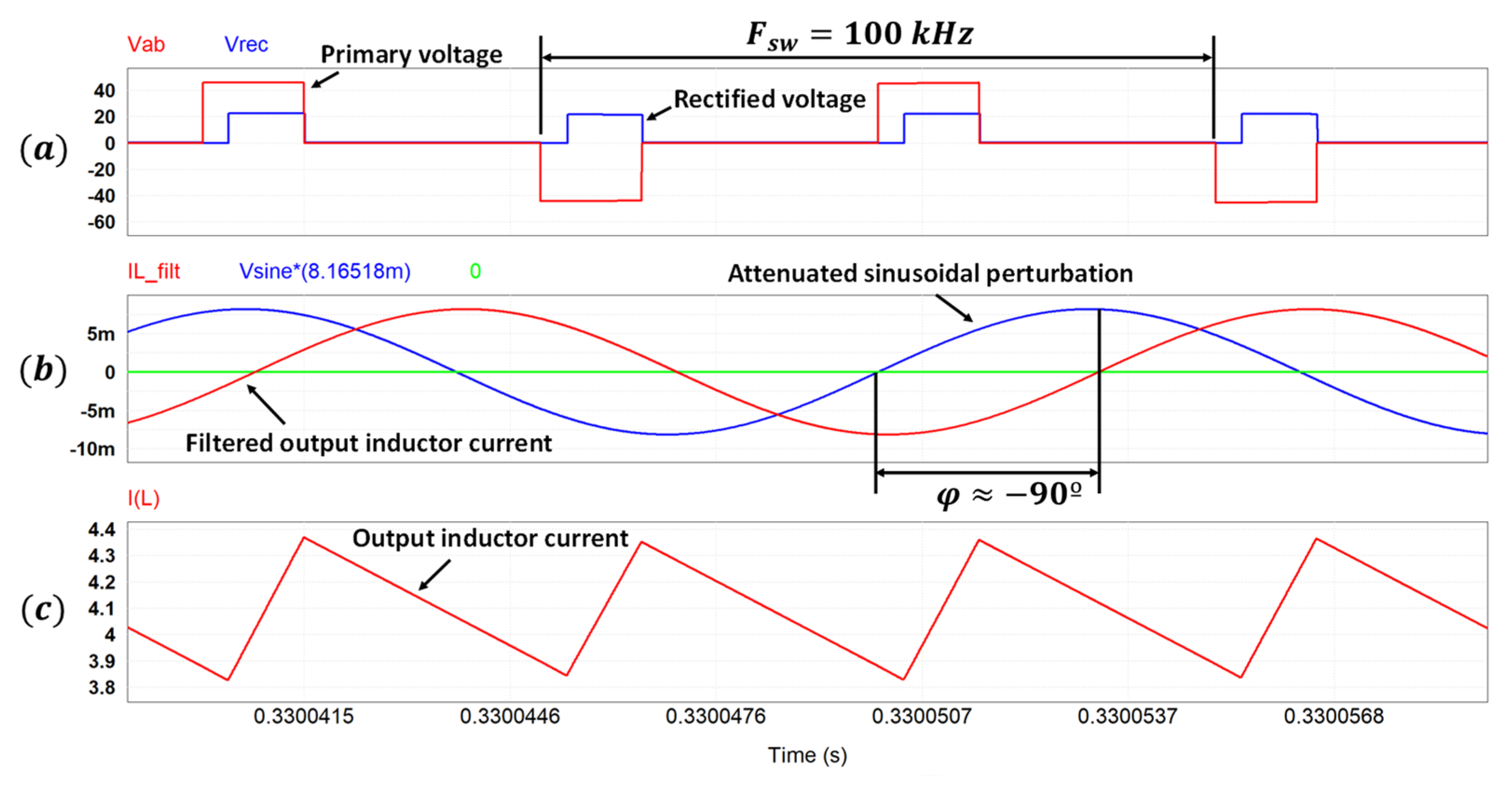
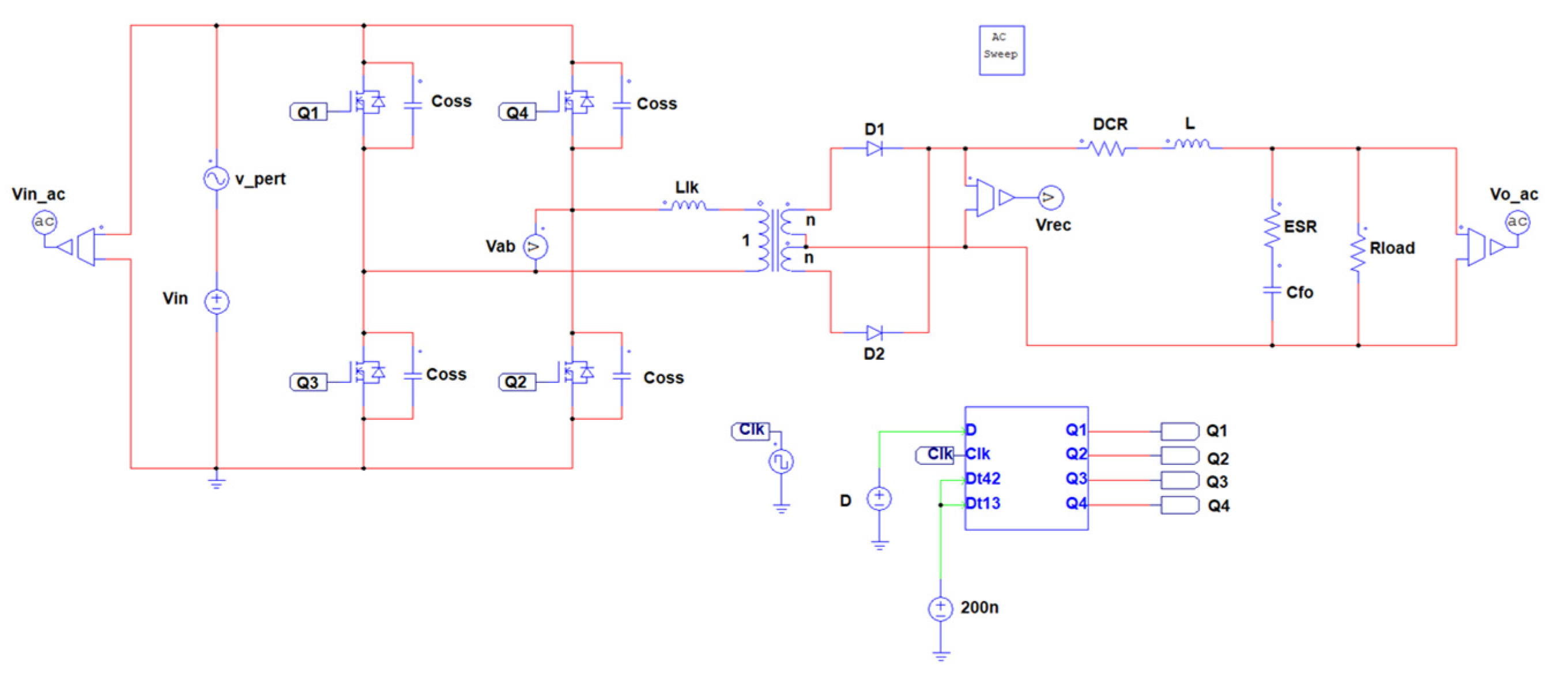
In order to check the effect that the input voltage perturbation has on the output inductor current, some simulations have been carried out using the PSIM software [31]. In these simulations, a periodic perturbation with fixed frequency is considered in order to observe how this delay that is present in the time domain affects the frequency response. In Figure 6, the schematic of the PSIM simulation is shown. The parameters of the first simulation are , , , , , , and . The ripple of the output inductor current is .
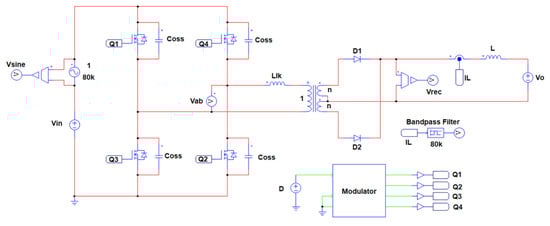
Figure 6.
PSIM schematic of the PSFB converter in which a sinusoidal perturbation is injected into the input voltage.
A sinusoidal perturbation, , with a frequency of 80 kHz is injected into the input voltage, as can be seen in Figure 6. The output inductor current is passed through a bandpass filter whose central frequency is 80 kHz, and thus, the phase difference that exists between input sinusoidal perturbation and the output inductor current is analyzed. In this simulation, the output voltage and the duty ratio are constant, so the small perturbation of and are equal to 0. Therefore, the input voltage to output inductor current transfer function is analyzed.
The blanking time is small and the interval is predominant, as can be seen in Figure 7a. In this test, the converter has a single pole, and the phase difference at high frequencies is expected to tend to −90°. The resulting phase difference between the input sinusoidal perturbation and the output inductor current is approximately −90°, as can be seen in Figure 7b. Figure 7c shows the output inductor current. From this test, it can be concluded that the interval does not introduce a delay in the frequency response despite being predominant. In this test, the delay introduced by the blanking time is very small because the blanking time interval is less than one-sixth of the switching period.
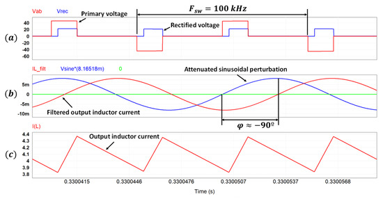
Figure 7.
Simulation results of Test 1. (a) Primary and rectified voltage. (b) Attenuated sinusoidal perturbation and output inductor current after bandpass filter. (c) Output filter inductor current.
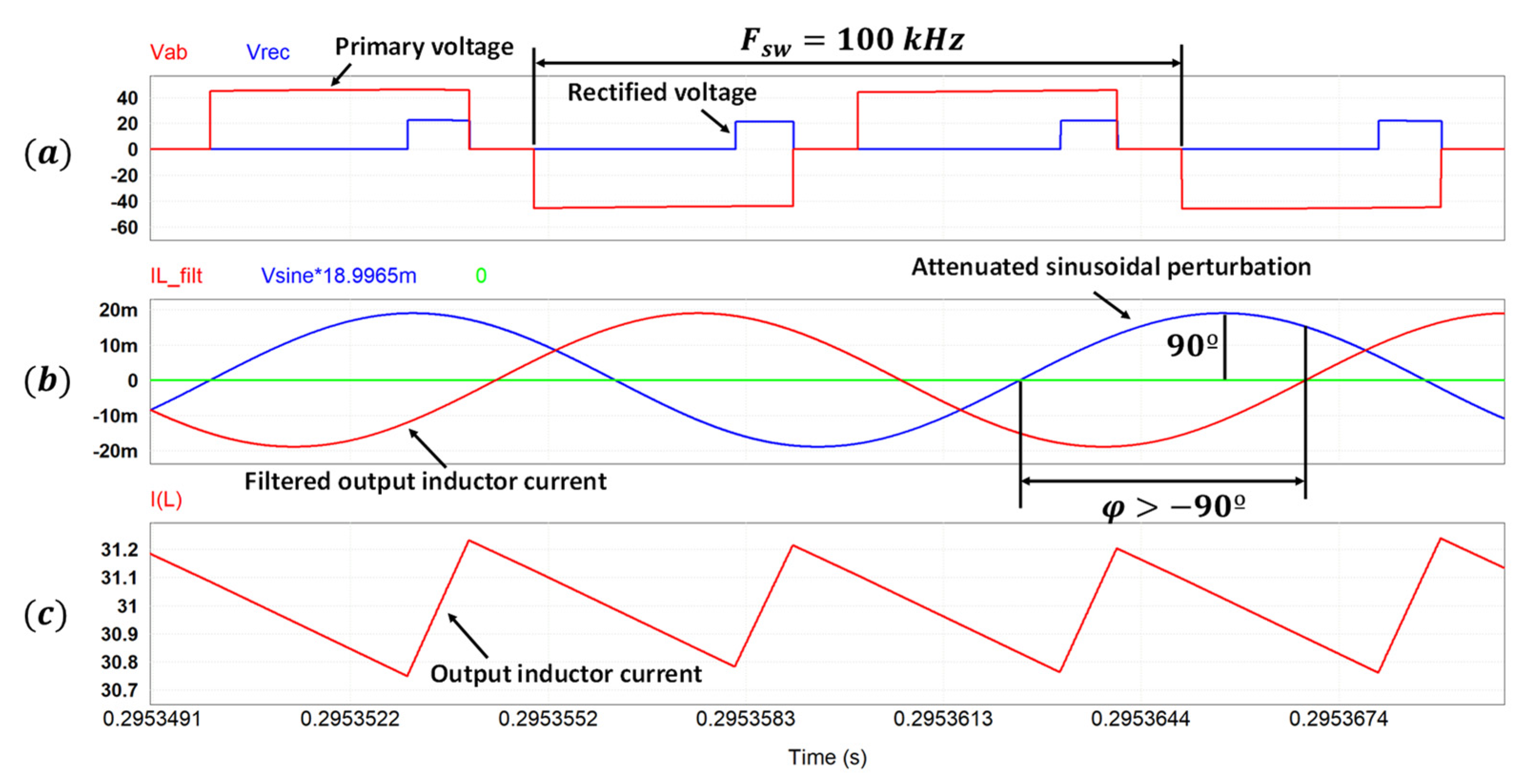
For the second test, the output voltage, , and the duty ratio, , have been changed to 4 V and 0.8, respectively. The PSIM schematic of Figure 6 is still valid for this test. The blanking time is noticeably increased, as can be seen in Figure 8a. The resulting phase difference between the input sinusoidal perturbation and the output inductor current is greater than −90°, as can be seen in Figure 8b. Figure 8c shows the output inductor current. From this test, it can be concluded that the delay that appears in the time domain also affects the frequency response. Having a considerable blanking time introduces an additional phase drop in the input voltage to the output inductor current transfer function.
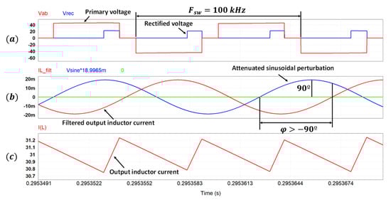
Figure 8.
Simulation results of Test 2. (a) Primary and rectified voltage. (b) Attenuated sinusoidal perturbation and output inductor current after bandpass filter. (c) Output filter inductor current.
Summarizing, the delay only affects the output inductor current in the case of small input voltage perturbation, so the characteristic coefficient of the output port is affected by the delay and is given by Equation (23). Expression (22) is still valid.
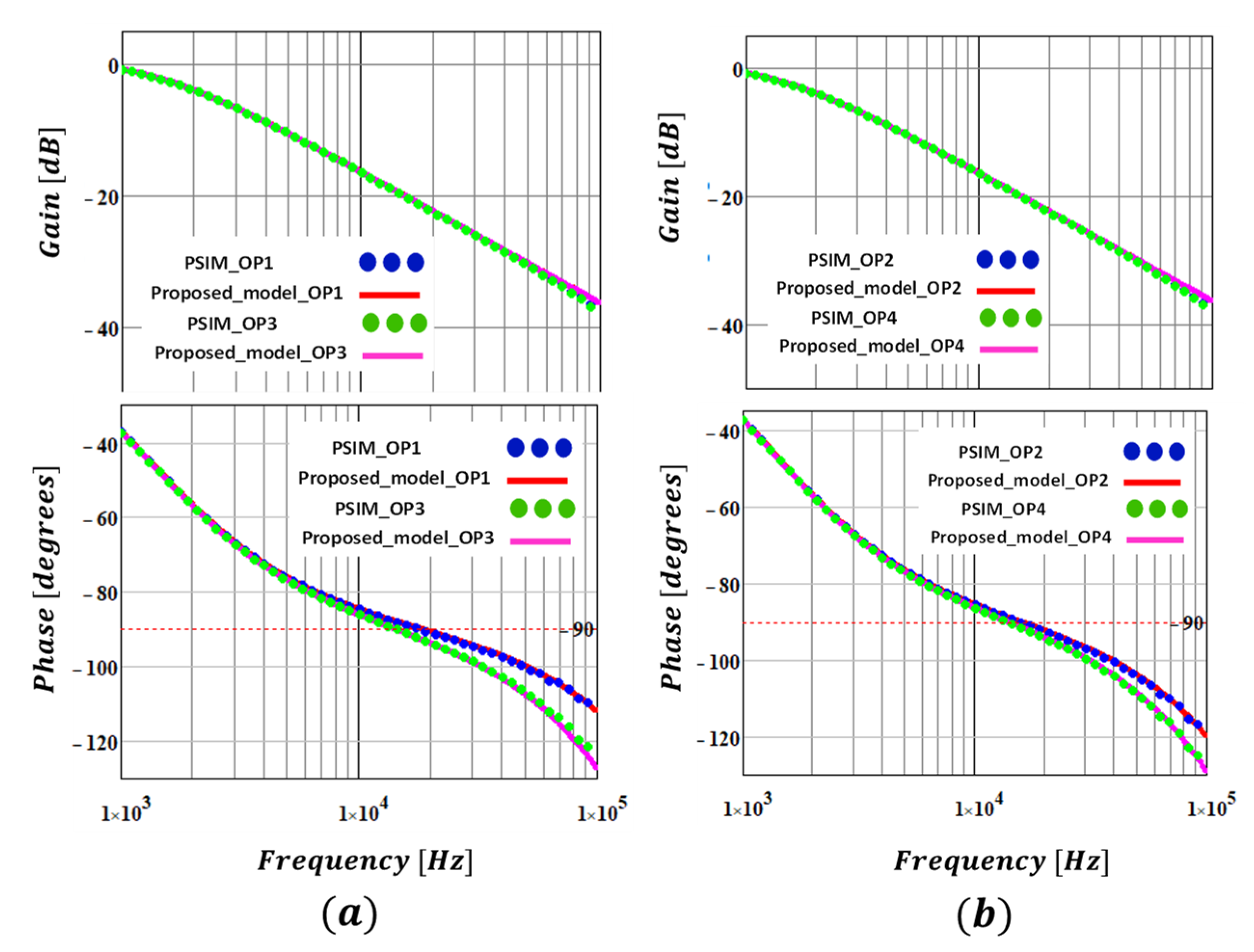
In order to quantify the value of in the frequency domain, the AC sweep tool of the PSIM software has been used. Therefore, the frequency response of the input voltage to output inductor current transfer function has been obtained for different operating points, OP. The simulation parameters are , , , , and . The different values of input voltages and output currents are shown in Table 1.

Table 1.
Parameters to obtain the frequency response at different operating points.
The comparison of the frequency response obtained from the simulation and proposed model is shown in Figure 9a,b. There is an excellent agreement between the proposed model and the simulation result. In Table 1, it can be seen that the value of is not fixed, which means that there is a random delay. However, its range is from 0 to .
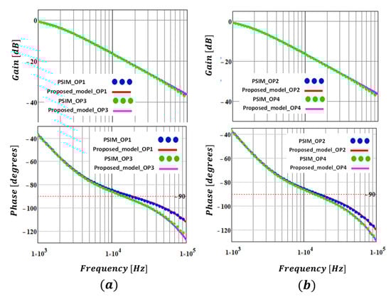
Figure 9.
Comparison of the frequency response. (a) Operating point 1 and 3. (b) Operating point 2 and 3.
In order to design a control loop that depends on the audio-susceptibility transfer function, the largest delay should be considered, which occurs when is equal to the blanking time. In this way, the stability of the control loop can be guaranteed.
The output inductor current dynamic response to a small output voltage step change is analyzed. If a small output voltage step occurs in any of the three intervals, then the output inductor current changes immediately, since the output inductor current slope always depends on the output voltage, as shown in Figure 10a,b. Therefore, there is no delay associated to the output port.
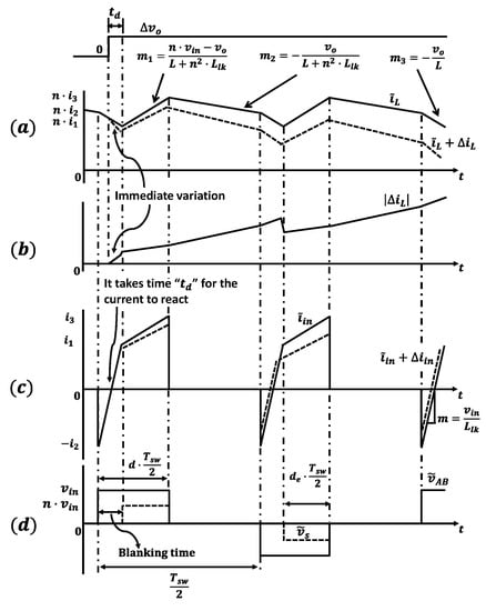
Figure 10.
Dynamic response to an output voltage step change. (a) Output inductor current, (b) incremental component of output inductor current, (c) input current and (d) primary and secondary voltage.
The input current dynamic response to a small output voltage step change is analyzed. If a small output voltage step occurs during the blanking time interval, then the input current does not change immediately since the input current slope does not depend on the output voltage, as shown in Figure 10c. The variation of the input current occurs after the blanking time interval has elapsed. Therefore, there is a delay associated to the blanking time. If the output voltage perturbation occurs in the interval , the input current varies immediately since the input current slope during this interval depends on the output voltage. Therefore, there is no delay associated with this interval. If the output voltage perturbation occurs during the interval , there is no delay, since it has the same effect as the case of the output inductor current response when an input voltage step is applied.
Summarizing, the delay only affects the input port in the case of small output voltage perturbation, so the characteristic coefficient of the input port is affected by the delay and is given by Equation (24). Expression (18) is still valid:
Finally, the output inductor current dynamic response and input current dynamic response is analyzed, when a perturbation is introduced into the duty ratio, . For this analysis, it is assumed that the duty ratio perturbation, , is applied in the interval , since it is a small-signal perturbation and has an effect on the PWM reset.
The perturbation of the duty ratio shown in Figure 11 has been exaggerated in order to clearly show the effect that causes on the waveforms of the converter. The duty ratio perturbation leads to an immediate change in the voltage as shown in Figure 11a. Since this change in occurs in the interval then the secondary voltage, , also changes as shown in Figure 11b. Therefore, and currents change instantaneously, as can be seen in Figure 11c,d. There is no delay in the input and output port. Expressions (17) and (20) are still valid.

Figure 11.
Dynamic response to a duty ratio step change. (a) Voltage at terminal A–B, (b) secondary voltage, (c) output inductor current and (d) input current.
In conclusion, from this analysis, it has been shown that the blanking time creates a delay in the input current when there is a small output voltage perturbation. This delay directly affects the coefficient . Likewise, the blanking time generates a delay in the output inductor current when there is a small input voltage perturbation. This delay directly affects the coefficient . The delay is random, since it depends on the moment in which the perturbation is injected until the interval begins. Its range is from 0 to . The final characteristic coefficients that represent the new small-signal model of the PSFB converter have been collected in Table 2.
Table 2.
Proposed characteristic coefficients of the PSFB converter.
4. Validation of the Small-Signal Model of the PSFB Converter by Simulation
The proposed model is validated by simulation using the AC sweep tool of the PSIM software. The open-loop audio-susceptibility transfer function has been selected, since it is the transfer function that best represents the effect of the delay produced by the blanking time. The validation by simulation was developed for three different operating points. The parameters for each operating point are shown in Table 3. The parameter represents the peak value of the modulator carrier signal. The simulation schematic is shown in Figure 12.
Table 3.
Parameters to obtain the frequency response at different power levels.
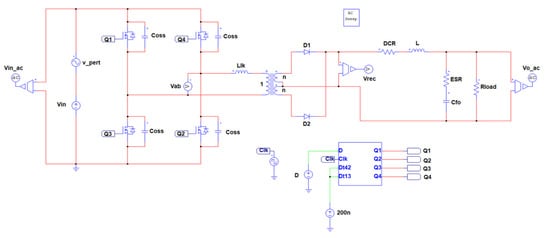
Figure 12.
PSIM schematic of the PSFB converter used for validation by simulation.
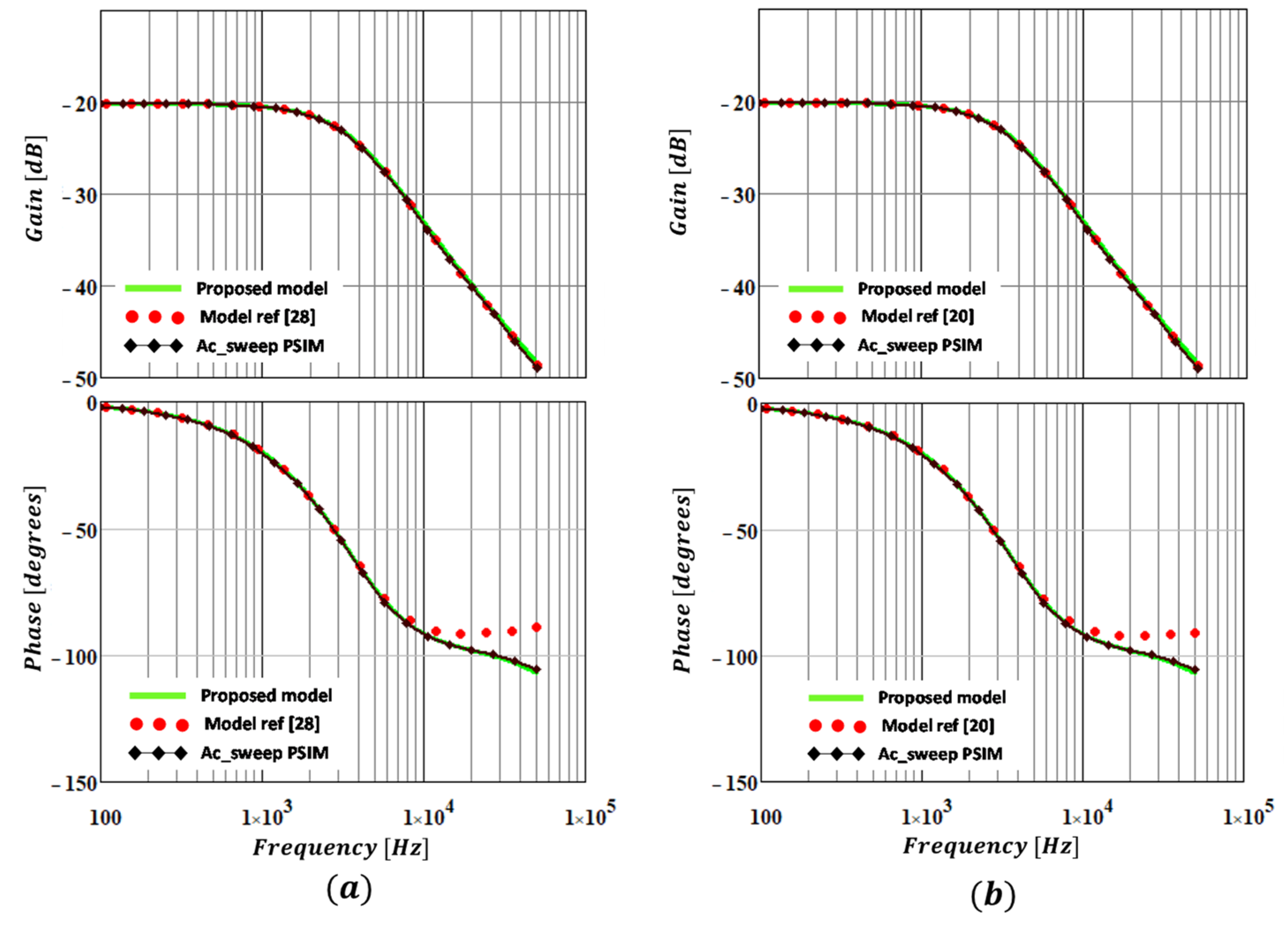
On the other hand, the small-signal model proposed in this paper is also compared with the small-signal models presented in [20,28].
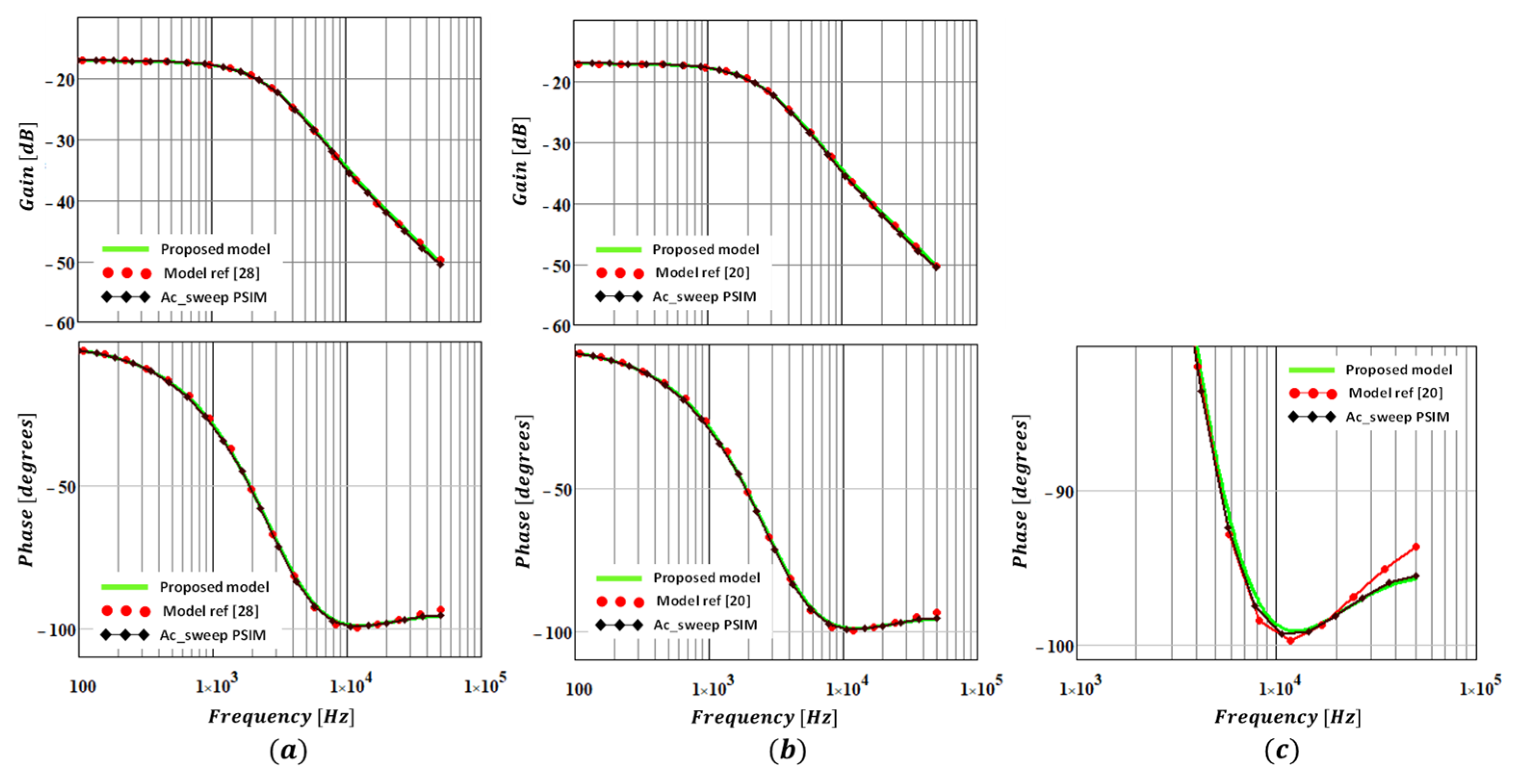
The validation for a power level of 90 W has been performed. For this operating point the blanking time represents approximately 5% of the duty ratio. Under these conditions, it can be seen in Figure 13a,b that the models presented in [20,28] apparently match with the frequency response obtained from PSIM software. In Figure 13c, a zoom of the phase in the high frequency region is shown. From Figure 13c, it can be seen that the model presented in [20] is not accurate in this frequency range. However, the proposed model allows to have a better estimation of the frequency response in this region.
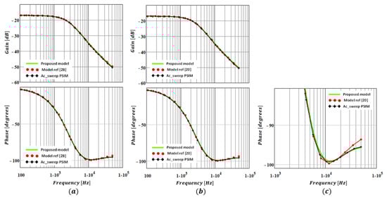
Figure 13.
Comparison of the frequency response of the audio-susceptibility transfer function for a power level of 90 W. (a) Proposed small-signal model vs. small-signal model presented in [28]. (b) Proposed small-signal model vs. small-signal model presented in [20]. (c) Phase zoom.
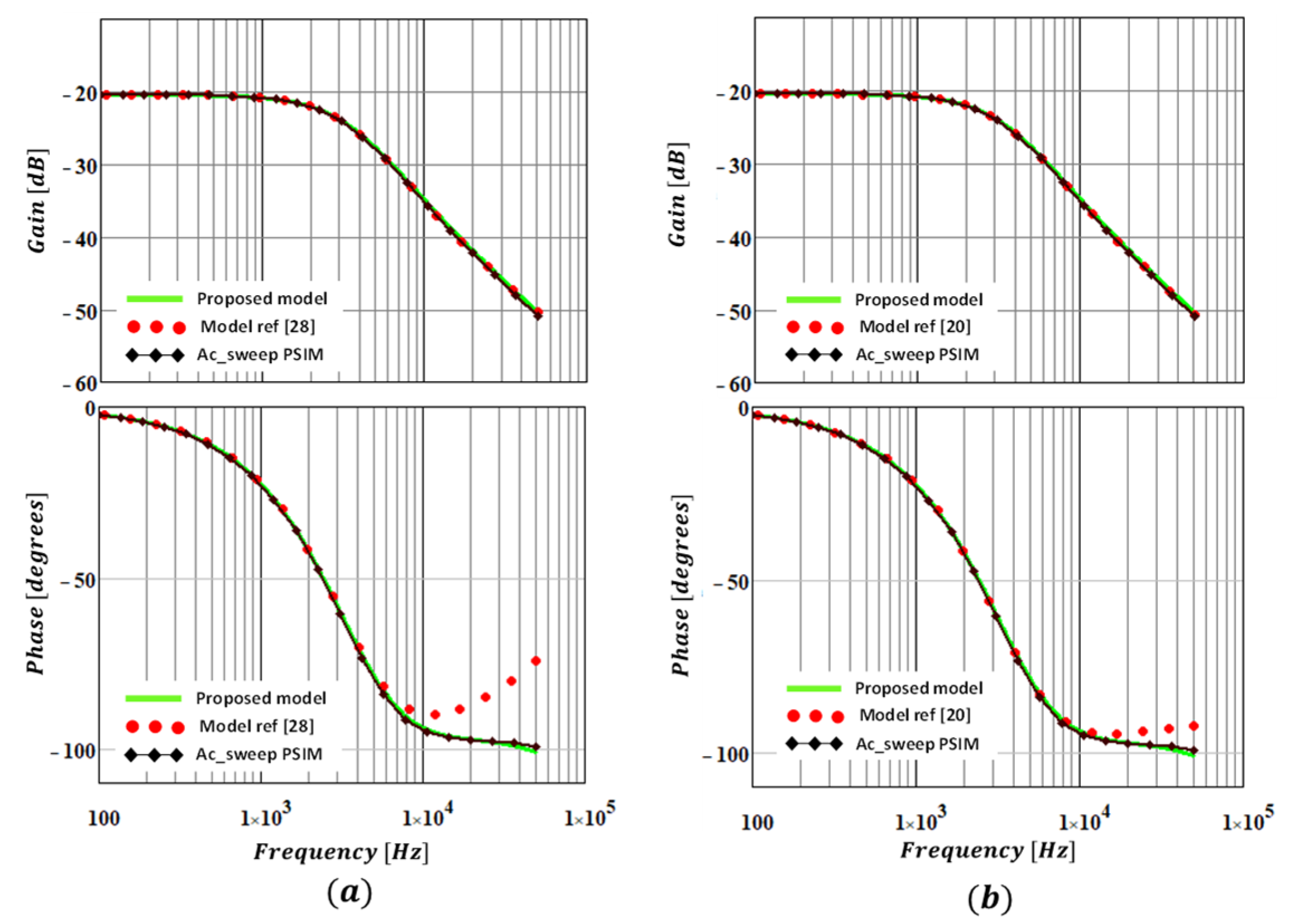
The validation for a power level of 250 W has been performed. From Figure 14a,b, it can be seen that the models presented in [20,28] are not able to predict the phase drop produced by the blanking time. However, the proposed model in this paper matches with the frequency response obtained from PSIM software. The delay considered in the proposed model is . For this operating point, the blanking time represents approximately 40% of the duty ratio.
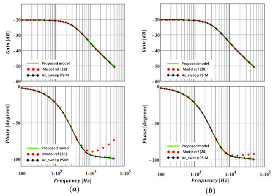
Figure 14.
Comparison of the frequency response of the audio-susceptibility transfer function for a power level of 280 W. (a) Proposed small-signal model vs. small-signal model presented in [28]. (b) Proposed small-signal model vs. small-signal model presented in [20].
Finally, the proposed model is validated for a power level of 500 W. From Figure 15a,b, it can be seen that the models presented in [20,28] do not predict the additional phase drop in the audio-susceptibility transfer function. For this operating point, the blanking time represents approximately 60% of the duty ratio.
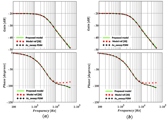
Figure 15.
Comparison of the frequency response of the audio-susceptibility transfer function for a power level of 500 W. (a) Proposed small-signal model vs. small-signal model presented in [28]. (b) Proposed small-signal model vs. small-signal model presented in [20].
From this validation, it can be concluded that if the power level is increased then the phase drop becomes more noticeable. This occurs because the blanking time is proportional to the load current, which means that if the load current is increased then the blanking time is increased. Therefore, the blanking time can become considerable even if the leakage inductor is small. On the other hand, it has been observed that the phase drop could occur before one-half of the switching frequency.
5. Experimental Validation of the Small-Signal Model of the PSFB Converter
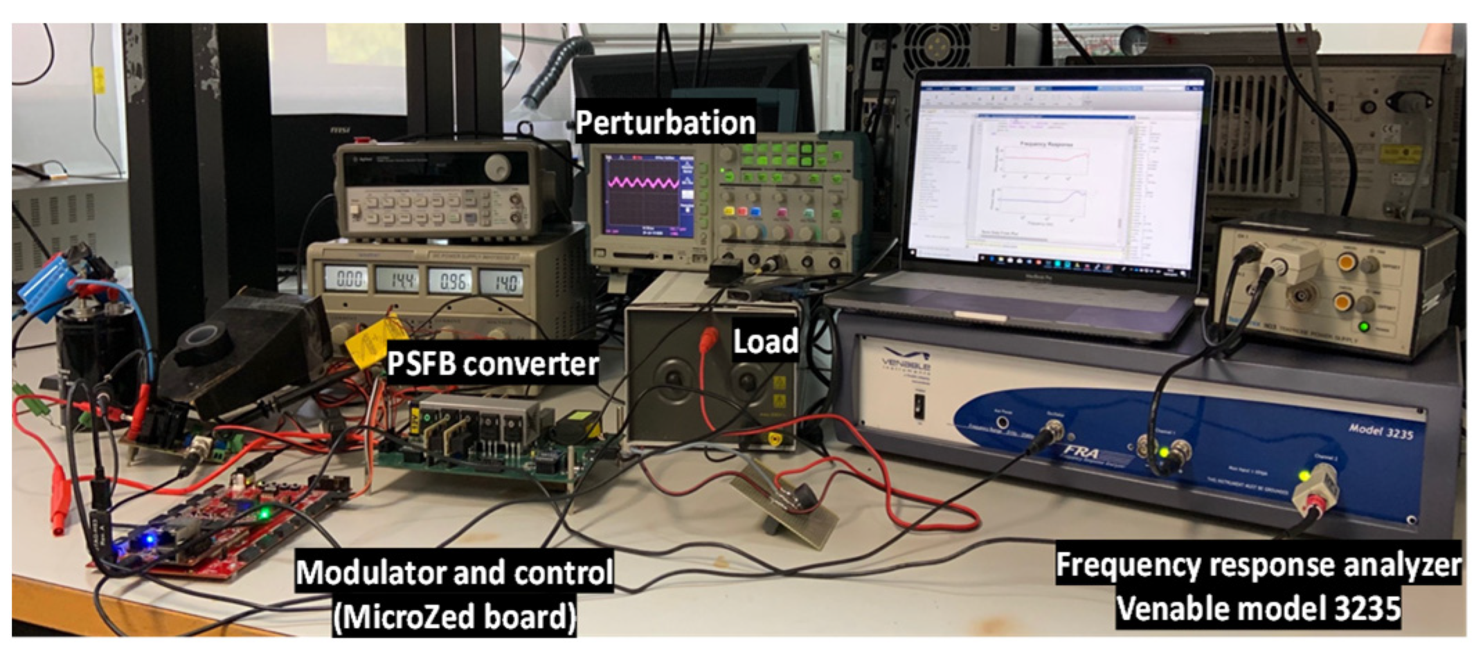
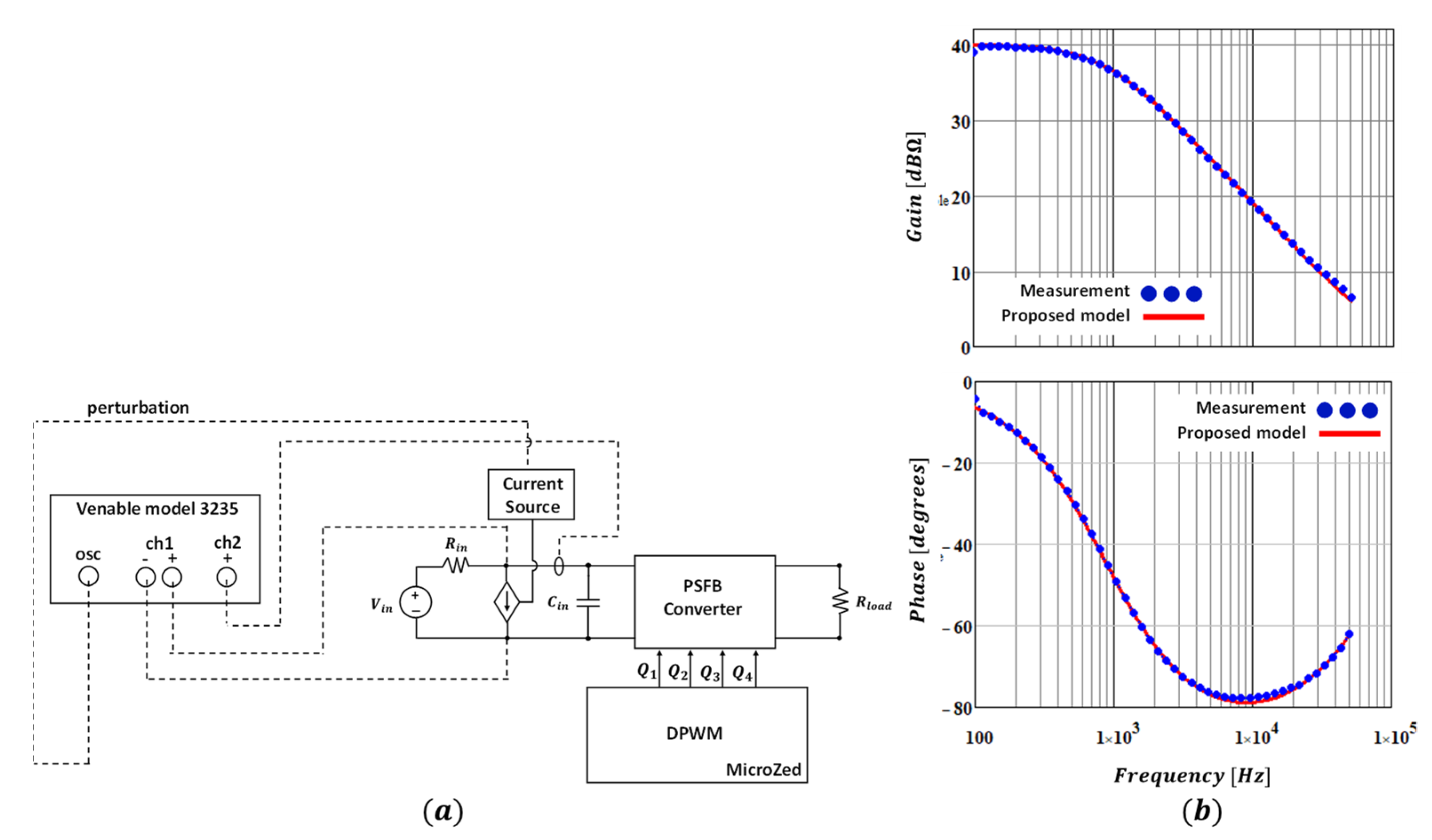
A prototype of Phase-Shifted Full-Bridge converter was built in order to experimentally verify the proposed small-signal model as shown in Figure 16. A leakage inductance that generates a significant blanking time has been selected in order to demonstrate that there is an excellent agreement between the proposed small-signal model and the experimental results. The converter is controlled by MicroZed board [32] based on a 7Z020 Xilinx Zynq device [33].
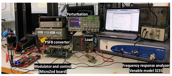
Figure 16.
Experimental prototype of the PSFB converter.
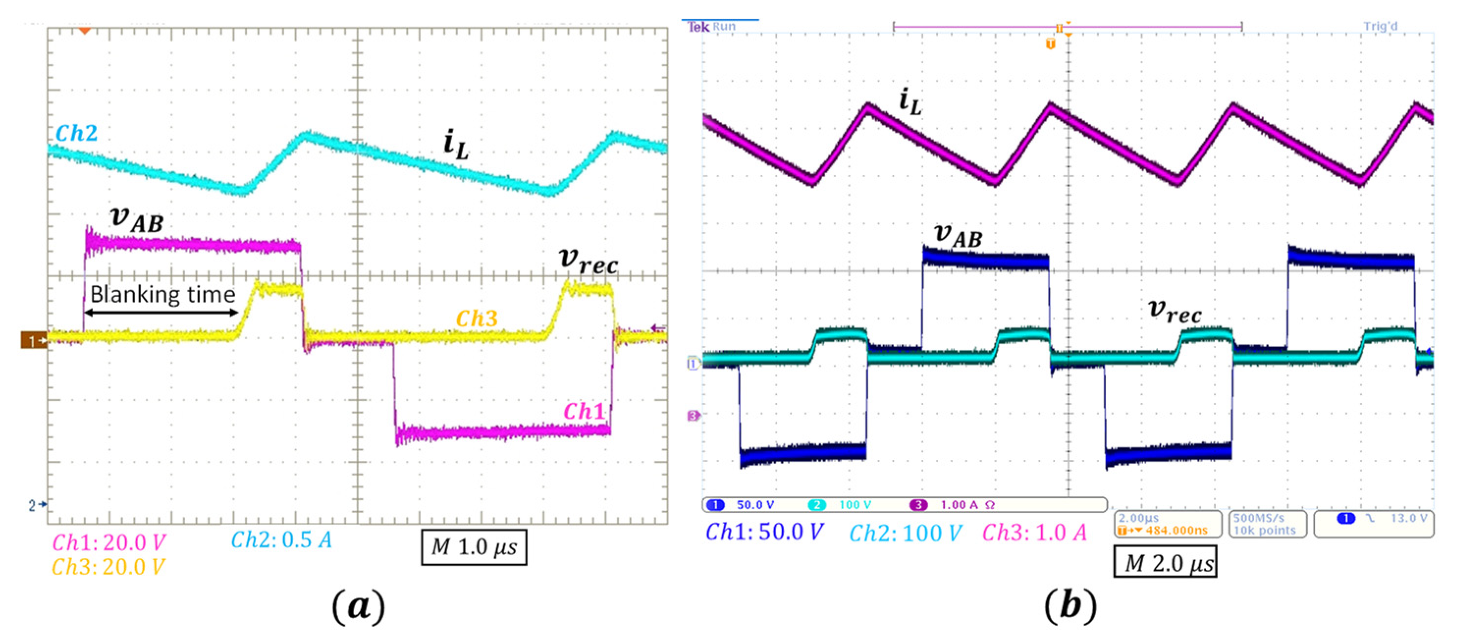
For the experimental validation, two different operating points have been selected. Figure 17a,b show the main waveforms for a power level of 8.5 W and 70 W, respectively. It can be seen that a large provokes a large blanking time.
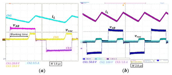
Figure 17.
Main waveforms of the experimental prototype at different power levels: (a) 8.5 W, (b) 70 W.
According to Figure 1, the main parameters for each operating point are found in Table 4. The validation shown in this section consists of obtaining the frequency response of the main transfer functions of the converter. The frequency response is obtained by using the Venable frequency response analyzer model 3235. The open-loop transfer functions are chosen to prevent that any delay from the digital control affecting the measurement.
Table 4.
Main parameters for each operating point.
5.1. Control to Output Voltage Transfer Function
The control to output voltage transfer function is given by Equation (25). The term represents the modulator gain:
where:
The impedance of the output filter capacitor and output filter inductor consider the parasitic resistances and are given by Equations (27) and (28), respectively:
From Equation (25), it can be deduced that the control to output voltage transfer function is not affected by the delay associated to the blanking time, since the characteristic coefficients and are not affected by the delay, as can be seen in Table 2. The measurement scheme is shown in Figure 18.
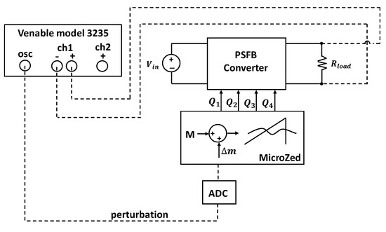
Figure 18.
Measurement block diagram of .
The perturbation has been generated using the Venable oscillator. This perturbation is passed through an analog-digital converter, ADC, with the aim of injecting the perturbation into the DPWM that is implemented in the MicroZed board. The ADC gain, modulator gain and the total delay (ADC delay plus DPWM delay) has been subtracted from the measurement in order to compensate these effects (post-processed).
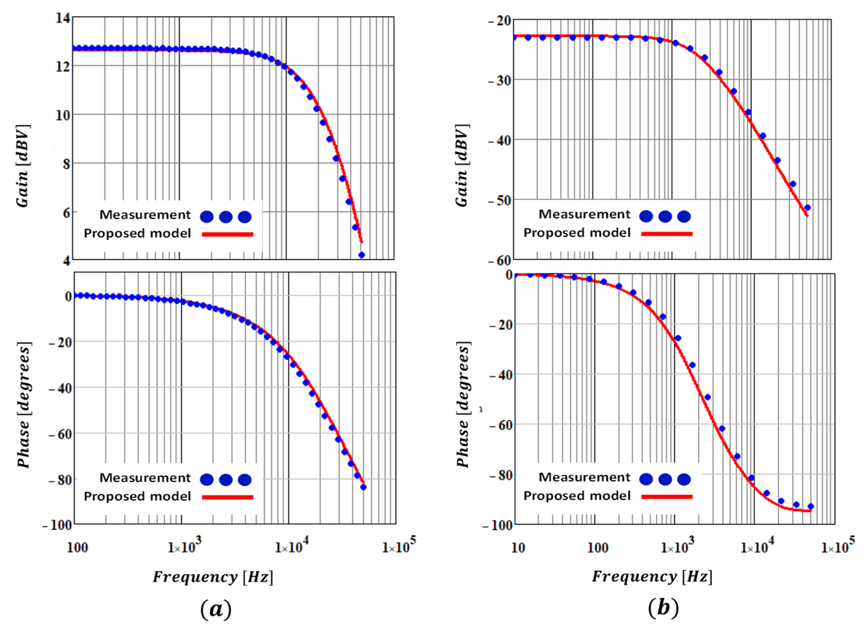
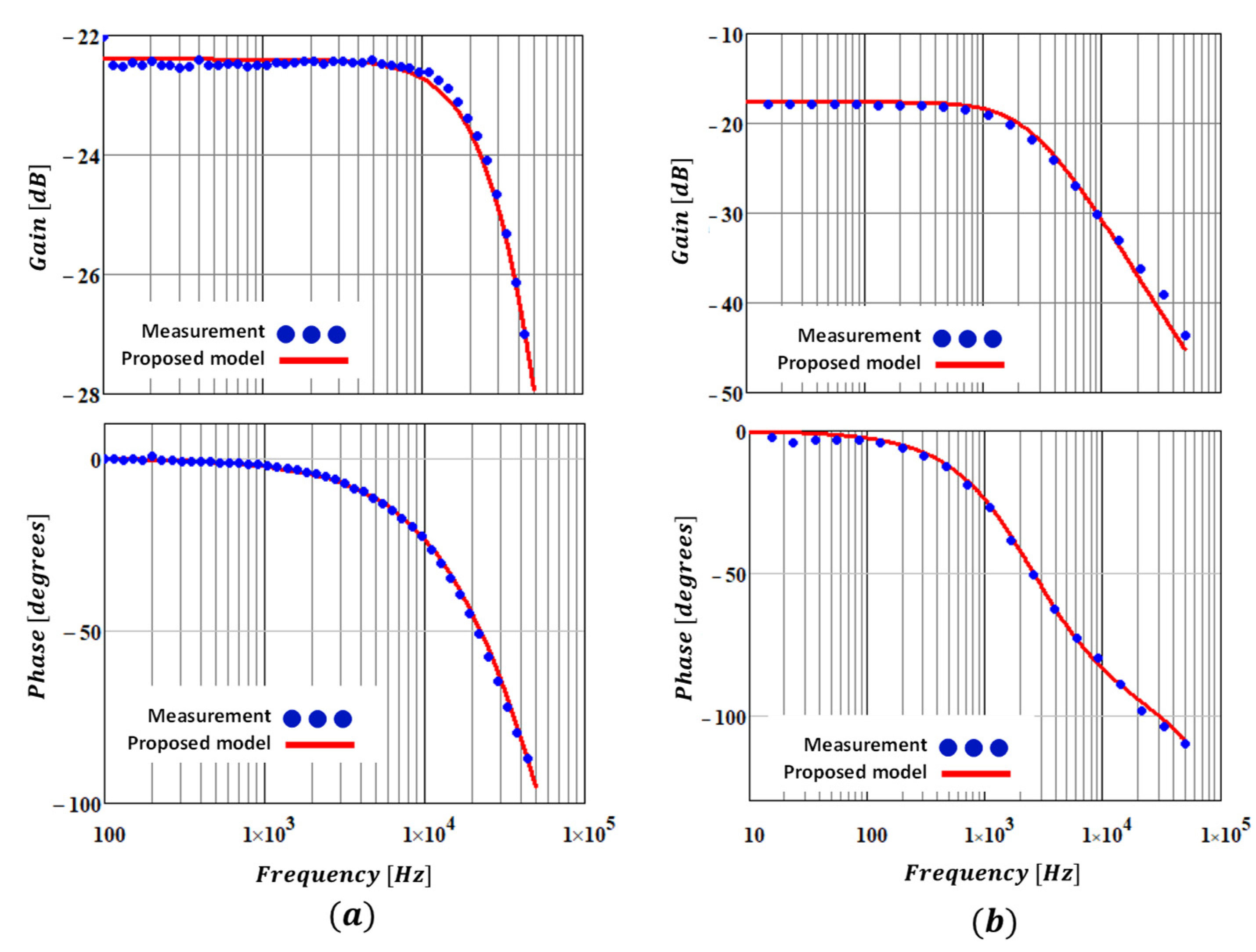
The magnitude and phase of the frequency response of the control to output voltage transfer function for the 8.5 W and 70 W power levels are shown in Figure 19a,b, respectively. There is an excellent agreement between the proposed model and the experimental results.
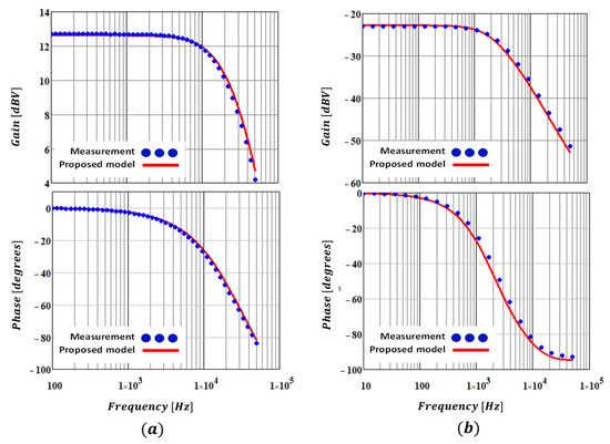
Figure 19.
Frequency response of control to output voltage transfer function. (a) 8.5 W. (b) 70 W.
5.2. Open-Loop Audio-Susceptibility Transfer Function
The open-loop audio-susceptibility transfer function is given by Equation (29):
From Equation (29), it can be deduced that the open-loop audio-susceptibility transfer function is affected by the random delay associated to the blanking time, since the characteristic coefficient is affected by the delay, as can be seen in Table 2.
The magnitude and phase of the frequency response of open-loop audio-susceptibility transfer function for the 8.5 W and 70 W power levels are shown in Figure 20a,b, respectively. There is an excellent agreement between the proposed model and the experimental results. The delay considered in this measure is in . However, the delay to consider may be different for other operating points due to its random nature, as mentioned in Section 3.
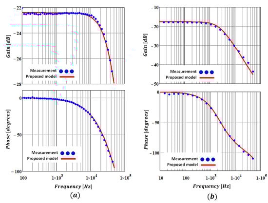
Figure 20.
Frequency response of open-loop audio-susceptibility transfer functions: (a) 8.5 W, (b) 70 W.
5.3. Open-Loop Input Impedance
The open-loop input impedance transfer function is given by Equation (30):
From Equation (30) it can be deduced that the open-loop input impedance is affected by the delay associated to the blanking time, since the characteristic coefficients and are affected by the delay, as can be seen in Table 2.
For the measurement of the input impedance, a high frequency decoupling capacitor, , has been added and its value is approximately . This measurement is not affected by any of the effects of digital control, since the current source amplifies the perturbation in an analog way as shown in Figure 21a. For the input impedance frequency response can be emphasized that the experimental measurement matches with the theoretical predictions, as shown in Figure 21b.
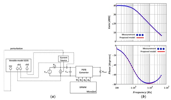
Figure 21.
(a) Measurement block diagram. (b) Frequency response of the open-loop input impedance, 8.5 W.
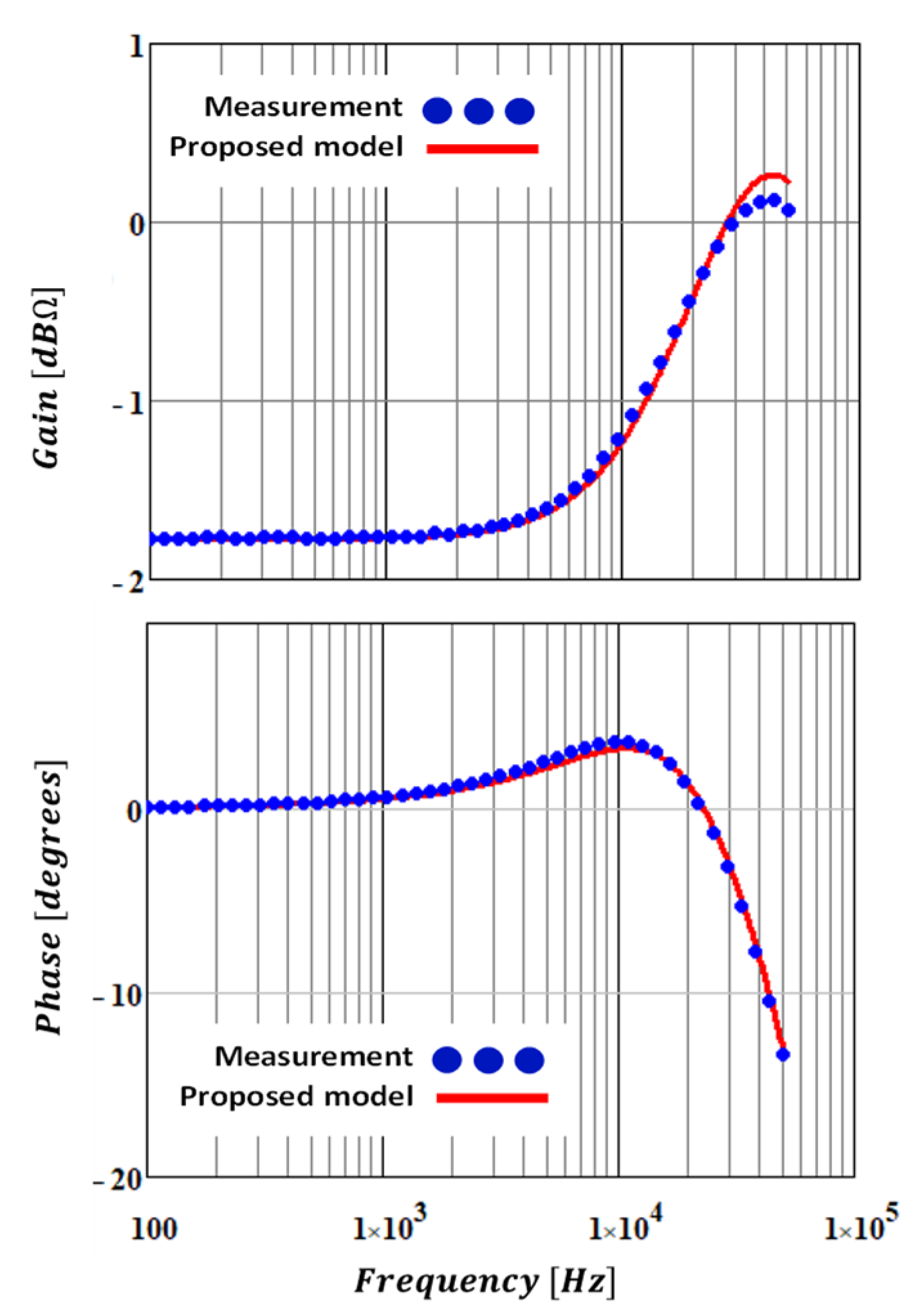
5.4. Open-Loop Output Impedance
The terminated open-loop output impedance transfer function (considering the load) is given by Equation (31):
From Equation (31), it can be deduced that the open-loop output impedance transfer function is not affected by the delay associated to the blanking time, since the characteristic coefficient is not affected by the delay, as can be seen in Table 2.
The magnitude and phase of the frequency response of the open-loop output impedance transfer function is shown in Figure 22. There is an excellent agreement between the proposed model and the experimental result.
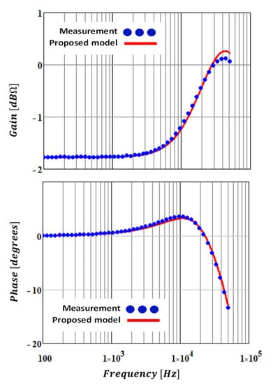
Figure 22.
Frequency response of the open-loop output impedance, 8.5 W.
6. Conclusions
A new small-signal model of the PSFB converter has been presented. This model predicts more accurately the gain of the transfer function because the additional switching stage due to the leakage inductance is considered. From the analysis of the natural response of the PSFB converter, it has been shown that in this topology, the blanking time creates a random delay in the input current response and the output inductor current response when there is a small output voltage perturbation and small input voltage perturbation, respectively. Therefore, the characteristic coefficients that are directly affected by this delay are and . The delay is variable since it depends on the moment in which the perturbation is injected until the interval begins. Its range is from 0 to . Therefore, in order to design a control loop that depends on audio-susceptibility transfer function, the largest delay should be considered, which occurs when is equal to the blanking time. The proposed small-signal model of the PSFB converter is capable of predicting the experimental phase drop that is generated in the audio-susceptibility transfer function when the blanking time is significant.
Author Contributions
D.O. did the theoretical analysis, circuit implementation, experimental testing and wrote the original draft paper. A.L. is the responsible for funding acquisition, investigation and supervision; his contribution was related to the theoretical analysis, paper reviewing and editing. P.Z. performed the investigation and his contribution was related to the theoretical analysis. M.S., J.R.d.F. and A.B. reviewed and contributed with useful comments on the paper’s structure and main paper contributions. All authors have read and agreed to the published version of the manuscript.
Funding
This research was funded by the European Regional Development Fund, the Ministry of Science, Innovation and Universities and the State Research Agency, grant number DPI2017-84572-C2-2-R.
Institutional Review Board Statement
Not applicable.
Informed Consent Statement
Not applicable.
Data Availability Statement
Not applicable.
Acknowledgments
This work is partially supported by the European Regional Development Fund, the Ministry of Science, Innovation and Universities and the State Research Agency through the research projects “Modelling and control strategies for the stabilization of the interconnection of power electronic converters”—CONEXPOT-2- (DPI2017-84572-C2-2-R) (AEI/FEDER, UE).
Conflicts of Interest
The authors declare no conflict of interest.
Nomenclature
| Injected-absorbed-current method | |
| Modulator transfer function | |
| Audio-susceptibility transfer function | |
| Control to output voltage transfer function | |
| Output impedance transfer function | |
| Input impedance transfer function | |
| Characteristic coefficients of the injected-absorbed-current method | |
| Impedances | |
| Transformer turns ratio (number of turns of the secondary winding divided by number of turns of the primary winding) | |
| Leakage inductance of the transformer | |
| Output filter inductance | |
| Blanking time interval | |
| Random delay | |
| Peak value of the modulator carrier signal | |
| Constant coefficients of the transfer function | |
| Operating point of the currents and voltages | |
| Switched currents and voltages | |
| Averaged and characteristic value of the currents and voltage | |
| Small-signal values of the currents and voltages |
Appendix A
The full set of the equations of the small-signal model of the PSFB converter is given below:
References
- Zhang, R.; Xu, H.; Wang, Y. A Dynamic Priority Factor Loop for Fast Voltage Equalization Applied to High Power Density DC–DC Converter System. IEEE Trans. Power Electron. 2020, 35, 198–207. [Google Scholar] [CrossRef]
- Lin, R.; Chou, H. MPPT photovoltaic wide load-range ZVS phase-shift full-bridge charger with DC-link current regulation. In Proceedings of the 2012 IEEE Industry Applications Society Annual Meeting, Las Vegas, NV, USA, 7–11 October 2012; pp. 1–8. [Google Scholar] [CrossRef]
- Whitaker, B.; Barkley, A.; Cole, Z.; Passore, B.; Martin, D.; McNutt, T.; Lostetter, A.; Lee, J.; Shiozaki, K. A High-Density, High-Efficiency, Isolated On-Board Vehicle Battery Charger Utilizing Silicon Carbide Power Devices. IEEE Trans. Power Electron. 2014, 29, 2606–2617. [Google Scholar] [CrossRef]
- Lim, C.; Jeong, Y.; Moon, G. Phase-Shifted Full-Bridge DC–DC Converter with High Efficiency and High Power Density Using Center-Tapped Clamp Circuit for Battery Charging in Electric Vehicles. IEEE Trans. Power Electron. 2019, 34, 10945–10959. [Google Scholar] [CrossRef]
- Naradhipa, A.M.; Kim, S.; Yang, D.; Choi, S.; Yeo, I.; Lee, Y. Power Density Optimization of 700kHz GaN-based Auxiliary Power Module for Electric Vehicles. IEEE Trans. Power Electron. 2021, 36, 5610–5621. [Google Scholar] [CrossRef]
- Ochoa, D.; Barrado, A.; Lázaro, A.; Vázquez, R.; Sanz, M. Modeling, Control and Analysis of Input-Series-Output-Parallel-Output-Series architecture with Common-Duty-Ratio and Input Filter. In Proceedings of the IEEE 19th Workshop on Control and Modeling for Power Electronics (COMPEL), Padua, Italy, 25–28 June 2018; pp. 25–28. [Google Scholar]
- Kim, C. Optimal Dead-Time Control Scheme for Extended ZVS Range and Burst-Mode Operation of Phase-Shift Full-Bridge (PSFB) Converter at Very Light Load. IEEE Trans. Power Electron. 2019, 34, 10823–10832. [Google Scholar] [CrossRef]
- Kalpana, R.; Kiran, R. Design and development of current source fed full-bridge DC-DC converter for (60V/50A) telecom power supply. In Proceedings of the 2017 International Conference on Technological Advancements in Power and Energy (TAP Energy), Kollam, India, 21–23 December 2017; pp. 1–6. [Google Scholar] [CrossRef]
- Baek, J.; Kim, C.; Lee, J.; Youn, H.; Moon, G. A Simple SR Gate Driving Circuit with Reduced Gate Driving Loss for Phase-Shifted Full-Bridge Converter. IEEE Trans. Power Electron. 2018, 33, 9310–9317. [Google Scholar] [CrossRef]
- Belkamel, H.; Kim, H.; Choi, S. Interleaved Totem-Pole ZVS Converter Operating in CCM for Single-Stage Bidirectional AC–DC Conversion with High-Frequency Isolation. IEEE Trans. Power Electron. 2021, 36, 3486–3495. [Google Scholar] [CrossRef]
- Gao, S.; Wang, Y.; Liu, Y.; Guan, Y.; Xu, D. A Novel DCM Soft-Switched SEPIC-Based High-Frequency Converter with High Step-Up Capacity. IEEE Trans. Power Electron. 2020, 35, 10444–10454. [Google Scholar] [CrossRef]
- Spro, O.C.; Lefranc, P.; Park, S.; Rivas-Davila, J.M.; Peftitsis, D.; Midtgard, O.; Undeland, T. Optimized Design of Multi-MHz Frequency Isolated Auxiliary Power Supply for Gate Drivers in Medium-Voltage Converters. IEEE Trans. Power Electron. 2020, 35, 9494–9509. [Google Scholar] [CrossRef]
- Wang, Y.; Song, Q.; Zhao, B.; Li, J.; Sun, Q.; Liu, W. Quasi-Square-Wave Modulation of Modular Multilevel High-Frequency DC Converter for Medium-Voltage DC Distribution Application. IEEE Trans. Power Electron. 2018, 33, 7480–7495. [Google Scholar] [CrossRef]
- Jang, Y.; Jovanovic, M.M. A New PWM ZVS Full-Bridge Converter. IEEE Trans. Power Electron. 2007, 22, 987–994. [Google Scholar] [CrossRef] [Green Version]
- Sabate, J.; Vlatkovic, V.; Ridley, R.; Lee, F.; Cho, B. Design considerations for high-voltage high-power full-bridge zero-voltage-switched PWM converter. In Proceedings of the IEEE Applied Power Electronics Conference and Exposition (APEC), Los Angeles, CA, USA, 11–16 March 1990; pp. 275–284. [Google Scholar] [CrossRef]
- Wu, X.; Zhang, J.; Xie, X.; Qian, Z. Analysis and optimal design considerations for an improved full bridge ZVS dc-dc converter with high efficiency. IEEE Trans. Power Electron. 2006, 21, 1225–1234. [Google Scholar] [CrossRef]
- Tran, D.; Vu, H.; Yu, S.; Choi, W. A Novel Soft-Switching Full-Bridge Converter with a Combination of a Secondary Switch and a Nondissipative Snubber. IEEE Trans. Power Electron. 2018, 33, 1440–1452. [Google Scholar] [CrossRef]
- Li, W.; Jiang, Q.; Mei, Y.; Li, C.; Deng, Y.; He, X. Modular Multilevel DC/DC Converters with Phase-Shift Control Scheme for High-Voltage DC-Based Systems. IEEE Trans. Power Electron. 2015, 30, 99–107. [Google Scholar] [CrossRef]
- Guo, Z.; Zhu, Y.; Sha, D. Zero-voltage-switching Asymmetrical PWM Full-bridge DC-DC Converter with Reduced Circulating Current. IEEE Trans. Power Electron. 2021, 68, 3840–3853. [Google Scholar] [CrossRef]
- Vlatkovic, V.; Sabate, J.A.; Ridley, R.B.; Lee, F.C.; Cho, B.H. Small-signal analysis of the phase-shifted PWM converter. IEEE Trans. Power Electron. 1992, 7, 128–135. [Google Scholar] [CrossRef]
- Cao, L. Small Signal Modeling for Phase-shifted PWM Converters with A Current Doubler Rectifier. In Proceedings of the 2007 IEEE Power Electronics Specialists Conference, Orlando, FL, USA, 17–21 June 2007; pp. 423–429. [Google Scholar] [CrossRef]
- Kim, T.; Lee, S.; Choi, W. Design and control of the phase shift full bridge converter for the on-board battery charger of the electric forklift. In Proceedings of the 8th International Conference on Power Electronics—ECCE, Jeju, Korea, 30 May–3 June 2011; pp. 2709–2716. [Google Scholar] [CrossRef]
- Capua, G.D.; Shirsavar, S.A.; Hallworth, M.A.; Femia, N. An enhanced model for small-signal analysis of the phase-shifted full-bridge converter. IEEE Trans. Power Electron. 2015, 30, 1567–1576. [Google Scholar] [CrossRef]
- Pai, K.; Li, Z.; Qin, L. Small-signal model and feedback controller design of constant-voltage and constant-current output control for a phase-shifted full-bridge converter. In Proceedings of the 2017 IEEE 3rd International Future Energy Electronics Conference and ECCE Asia (IFEEC 2017—ECCE Asia), Kaohsiung, Taiwan, 3–7 June 2017; pp. 1800–1805. [Google Scholar] [CrossRef]
- Huang, C.; Chiu, H. A PWM Switch Model of Isolated Battery Charger in Constant-Current Mode. IEEE Trans. Ind. Appl. 2019, 55, 2942–2951. [Google Scholar] [CrossRef]
- Ahmed, M.R.; Wei, X.; Li, Y. Enhanced Models for Current-Mode Controllers of the Phase-Shifted Full Bridge Converter with Current Doubler Rectifier. In Proceedings of the 2019 10th International Conference on Power Electronics and ECCE Asia (ICPE 2019—ECCE Asia), Busan, Korea, 27–30 May 2019; pp. 3271–3278. [Google Scholar]
- Vorperian, V. Simplified analysis of PWM converters using model of PWM switch. Continuous conduction mode. IEEE Trans. Aerosp. Electron. Syst. 1990, 26, 490–496. [Google Scholar] [CrossRef]
- Schutten, M.J.; Torrey, D.A. Improved small-signal analysis for the phase-shifted PWM power converter. IEEE Trans. Power Electron. 2003, 18, 659–669. [Google Scholar] [CrossRef]
- Kislovski, A. General small-signal analysis method for switching regulators. In Proceedings of the 4th Annual International PCI Conference, San Francisco, CA, USA, 29–31 March 1982; pp. 1–15. [Google Scholar]
- Kislovski, A.; Redl, R.; Sokal, N.O. Dynamic Analysis of Switching Mode DC/DC Converters; Van Nostrand Reinhold: New York, NY, USA, 2012. [Google Scholar]
- POWERSYM Inc. PSIM User’s Manual 2020a. Available online: https://www.powersimtech.com/wp-content/uploads/2021/01/PSIM-User-Manual.pdf, (accessed on 10 August 2021).
- AVNET. Microzed Getting Started Guide. Available online: https://www.avnet.com/wps/wcm/connect/onesite/0f5bc224-0117-44b3-a3f4-23bb1f7da3c0/MicroZed_GettingStarted_v1_2.pdf?MOD=AJPERES&CACHEID=ROOTWORKSPACE.Z18_NA5A1I41L0ICD0ABNDMDDG0000-0f5bc224-0117-44b3-a3f4-23bb1f7da3c0-nNnX57 (accessed on 5 April 2020).
- XILINX. Zynq-7000 SoC Technical Reference Manual. Available online: https://www.xilinx.com/support/documentation/user_guides/ug585-Zynq-7000-TRM.pdf (accessed on 20 April 2020).


Publisher’s Note: MDPI stays neutral with regard to jurisdictional claims in published maps and institutional affiliations. |
© 2021 by the authors. Licensee MDPI, Basel, Switzerland. This article is an open access article distributed under the terms and conditions of the Creative Commons Attribution (CC BY) license (https://creativecommons.org/licenses/by/4.0/).