1. Introduction
DC-DC converters play a key role in energy conversion and conditioning applications that require reduced weight and size, such as electric and hybrid vehicles, aeronautical equipment, space probes and satellites, renewable energy systems, among other applications [
1,
2,
3]. With regard to the development of topologies for DC-DC converters, there is a trend in the search for equipment with a higher power density, and advances are mainly motivated by the requirements of lower cost and volume [
4]. In this scenario, researchers have been focused on finding ways to improve and overcome the limitations in the power processing capacity of classic DC-DC converters. Among the various approaches, the soft switching techniques can be mentioned, which lead to greater efficiency in energy conversion, but the cost and complexity increase due to the multiple elements of the resonant tank network [
5].
The interleaving technique in power electronics converters is the usual solution to achieve high power levels and modularity, however, the appropriate current sharing between the association of multiple cells should be taken into consideration, which demands the use of sophisticated control schemes to maintain the current balance between the semiconductors [
6]. Similar to interleaving solutions, the three-state switching cell (3SSC) was introduced in [
7], being an interesting solution for increasing power density, with a high efficiency level, and without the need for special control strategies.
Since the 3SSC was proposed, a variety of topologies for DC-DC, AC-DC, and DC-AC converters have been presented in the literature [
8,
9,
10]. All of these approaches present interesting advantages inherent to the application of the 3SSC, i.e., reduction of weight and volume of the filter elements, current stress division between the semiconductors and, consequently, distribution of the losses, providing the reduction of the heat-sink’s size [
11,
12,
13]. Although the 3SSC uses a high-frequency autotransformer, its dimensions are compact, because that element operates at twice the switching frequency and only in two quadrants of the B-H curve [
14].
It is noteworthy that most of the applications with 3SSC mainly use the type-B cell (3SSC-B) topology [
15]. It could be associated with the fact that the 3SSC-B-based buck, boost and buck-boost converters have a static gain identical to the classic non-isolated converters, in the whole range of duty cycle, when they operate in continuous conduction mode (CCM). This characteristic has been an attractive solution for the development and exploration of new non-insulated step-up DC-DC structures by employing the 3SSC-B [
16,
17,
18,
19].
Nevertheless, a characteristic of classic boost converters, including the 3SSC-B-based boost, is the right-half-plane (RHP) zero in the control-to-output-voltage transfer function in CCM. This fact causes the non-minimum phase characteristic, imposing limitations for the bandwidth and the dynamic response in the control-loop by using single-loop control architectures, i.e., to ensure stability with adequate damping [
20]. These limitations have motivated the effort to develop step-up structures that have a satisfactory dynamic performance without the need to apply cascade or complex control architectures [
21,
22,
23].
In this context, the DC-DC 3SSC-A-based boost topology, initially proposed by [
7] and briefly explored by the authors in [
24], becomes an interesting alternative in step-up converters with minimum phase characteristic, where a faster dynamic response can be attended by employing a simple closed-loop control scheme with a single-loop control, which also reduces computational and signal conditioning costs in practical implementations.
Therefore, taking into account the reduced amount of research that employs the 3SSC-A and the advantages presented by 3SSC-based converters, this paper fills a gap in the literature with the following contributions:
A generalized and detailed static analysis of the DC-DC 3SSC-A-based boost converter, including highlighting the discontinuous conduction mode (DCM) and critical conduction mode (CRM).
A complete theoretical study of voltage and current stresses in semiconductors, comparison with other step-up structures with minimum phase characteristics, description of a loss model in all components, as well as the validation of the small-signal model by simulation results.
Verification of the dynamic response of the control scheme with a single-loop architecture and the efficiency under several load conditions by experimental results.
This paper is organized as follows,
Section 2 describes the converter analysis, including loss models, modeling and design considerations. A comparison with similar converters is detailed in
Section 3.
Section 4 presents the experimental validations, followed by the final considerations.
2. The 3SSC-A-Based Boost: Static Analysis
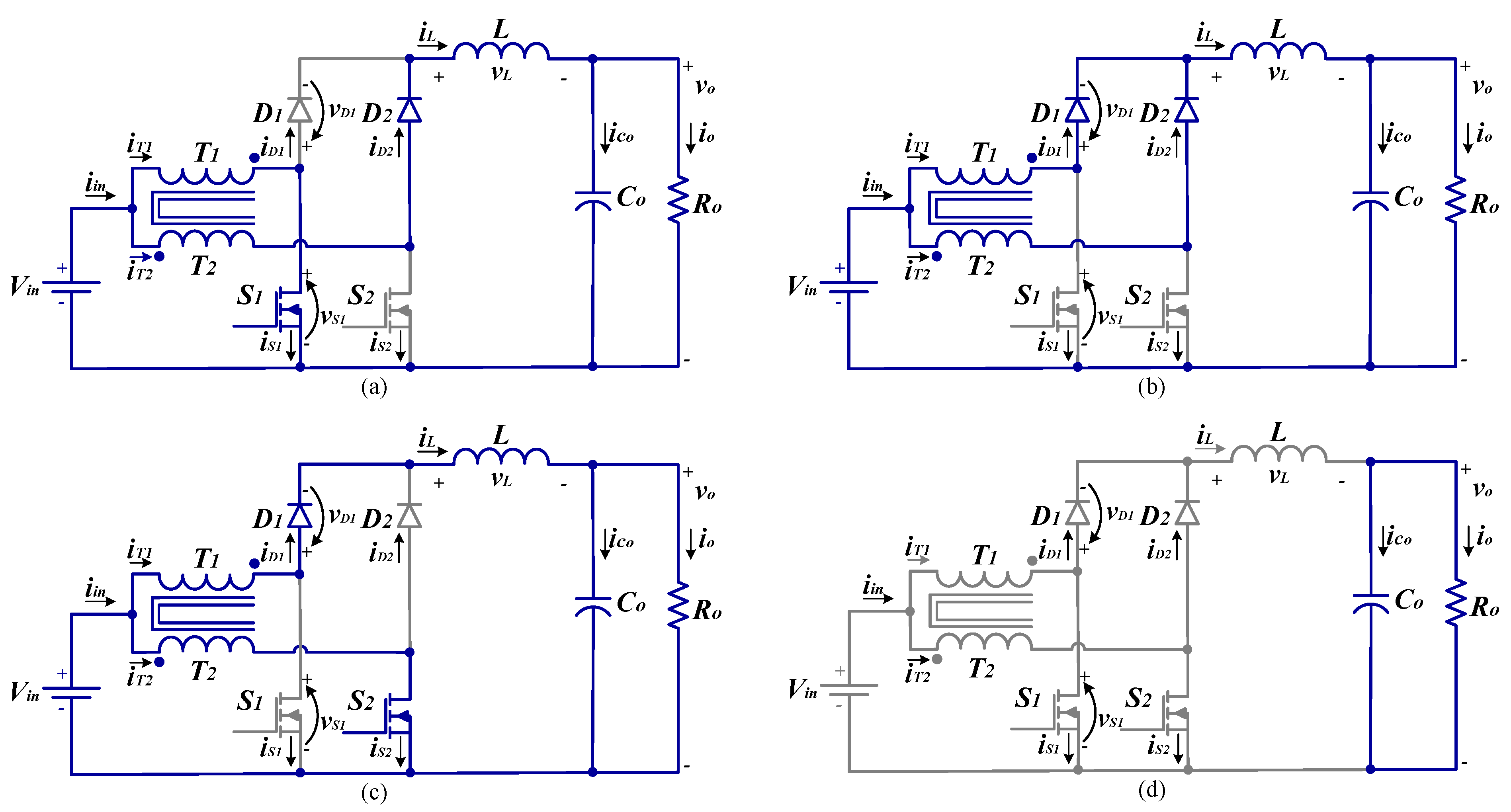
The 3SSC-A-based boost converter consists of an autotransformer with windings (
,
), two controlled switches (
,
), two diodes (
,
), one inductor (
L), and an equivalent load (
) connected in parallel with the output capacitor (
), as shown in
Figure 1. This topology must operate with a duty cycle less than 0.5, in order to avoid the switches working on overlapping condition, which could be considered as a disadvantage of the 3SSC-A-based converters. In this section, the operation principle in steady state is analyzed.
2.1. Operation Principle
The operation principle study of the 3SSC-A-based boost converter is accomplished under CCM, DCM, and CRM, by considering all of converter’s components as ideal elements, with electrical variables defined as follows:
—command signals of switches and ;
—input current;
— switch current;
— diode current;
—inductor current,
—load current;
—capacitor current;
— switch voltage;
— diode voltage;
—inductor voltage.
2.1.1. CCM
The equivalent circuits in CCM and the main theoretical waveforms, defined according to four operation modes, are shown in
Figure 1a–c and
Figure 2a, respectively.
First Stage () (Figure 1a)
Initially, the switch is turned on, while the switch is turned off. The autotransformer’s windings’ currents are equivalent to half of the input current , which is guaranteed by the unitary turns ratio and, consequently, the voltages on the windings and are equal to . Thus, the current flows through the switch , the current flows through the diode and the inductor L stores energy. Considering that the autotransformer’s windings have the same impedance, the voltages on and are equal and equivalent to .
Second Stage () (Figure 1b)
The switch is turned off and the diode is turned on. While and remain turned off and turned on, respectively. The current flowing through and and the magnetic flux in the autotransformer core is null. Thus, the polarity of is inverted and the stored energy in the inductor L is transferred to the load.
Third Stage () (Figure 1c)
This stage is similar to the operation stage 1, where, the switch is turned on and remains turned off. The diode continues turned on and is turned off.
Fourth Stage () (Figure 1b)
This stage is identical to the second stage, where the inductor current flows through the diodes , and the autotransformer windings.
2.1.2. DCM
This operation mode present six equivalent operation stages defined according to the theoretical waveforms shown in
Figure 2b. Some of the operation stages in DCM are equivalent to the CCM and these will not be described in detail.
First Stage () (Figure 1a)
This stage is identical to the first stage in CCM.
Second Stage () (Figure 1b)
This stage is identical to the second stage when the converter is operating in CCM.
Third Stage () (Figure 1d)
In this stage, the current in the inductor becomes zero, the switches and remain turned off, and diodes and are turned off. Thus, there is not power transfer from the input source to the load. The power supplied to the load comes from the output capacitor.
Fourth Stage () (Figure 1c)
Identical to the third stage of the CCM.
Fifth Stage () (Figure 1b)
Identical to the fourth stage of the CCM.
Sixth Stage ()
Identical to the third stage of the DCM.
In
Figure 2b, it is verified that the current in the inductor is null during the third and sixth operation stages, characterizing the DCM. Semiconductors are subjected to a maximum voltage equivalent to twice the input voltage
.
2.1.3. CRM
In this mode, maintaining the 180-degree delay, each switch is turned on at the exact moment when the current in the inductor becomes null, causing the current to increase again. The inductor current becomes null every half-time, so the minimum current is equal to zero and the current ripple in the inductor is equal to its maximum current . The first and second operation stages in CRM are equivalent to the first and second stages in DCM, respectively.
2.1.4. Output Characteristic of the Converter
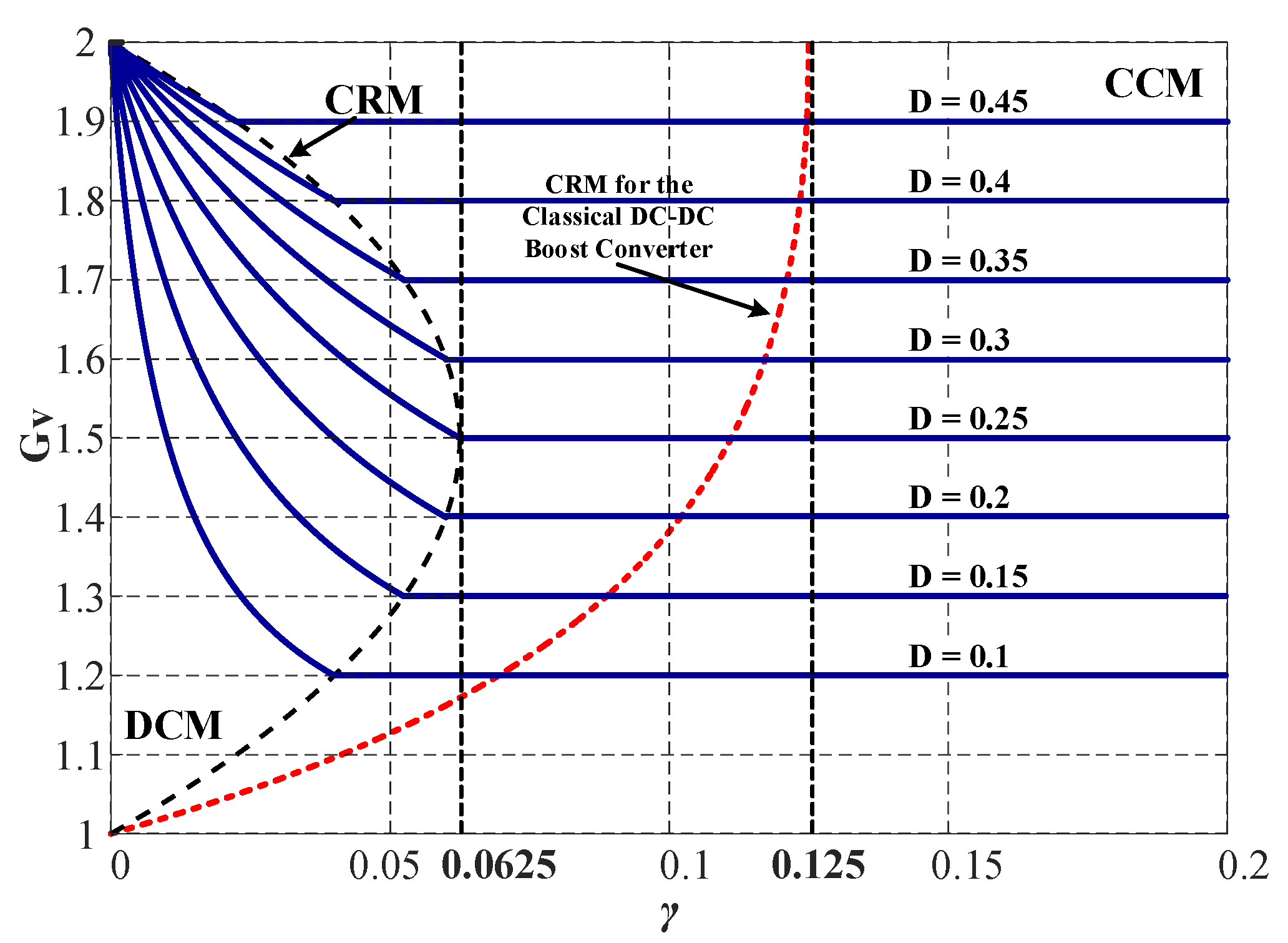
The static gain for each operation mode: CCM, DCM, and CRM are expressed as (
1), (
2), and (
3) respectively.
where,
is the average output current,
is the switching frequency,
D is the duty cycle, and
represents the normalized output current, defined in (
4).
From (
1)–(
3), the static gain curves of the proposed converter are presented in
Figure 3. Analogously to the classic boost converter, the output voltage is a function of the load current in DCM. The maximum static gain in CRM occurs at
= 0.0625 and
D = 0.25 for the 3SSC-A-based boost converter, which differs from the classic boost converter, whose maximum gain in CRM occurs at
and
. In this regard, the CCM region is wider for the 3SSC-A-based boost converter, i.e., for the same operating point, the inductance becomes half of that required for the classical boost converter.
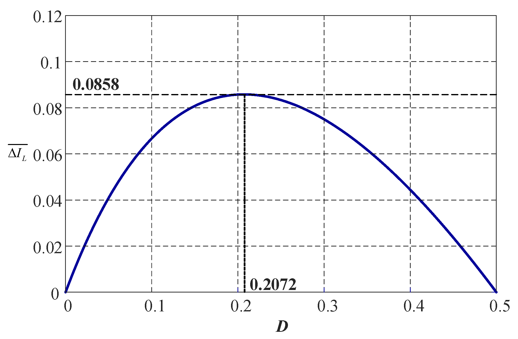
2.1.5. Filter Elements
The inductor current ripple
, described in (
5), can be obtained applying Kirchhoff’s voltage law to
Figure 1a.
The normalized current ripple
is given by (
6) and plotted in
Figure 4, where it can be seen that the maximum value occurs at
.
The inductance
L is determined by reorganizing (
5), according to (
7).
The critical inductance
, described in (
8), corresponds to the threshold value of inductance between CCM and DCM. From
Figure 3, the threshold value of
is 0.0625, and the critical inductance is calculated by replacing that value in (
4).
Considering the charge variation on the capacitor
during a switching period, the minimum capacitance required to obtain the desired voltage ripple
is given by (
9).
2.2. Semiconductors Stresses in CCM
The average and RMS values of the switches currents are given by (
10) and (
11), respectively.
The average and RMS values of the diodes currents are given by (
12) and (
13), respectively.
The maximum voltage stress across the switches and diodes is given by (
14) and (
15), respectively.
Semiconductor losses are described according to [
25,
26]. Hence, the conduction and switching losses of the IGBT are given by (
16) and (
17), respectively.
where
is the peak of the current switch,
is the collector–emitter saturation voltage, and
and
are the turn-on and turn-off switching times. For the diodes, only the conduction losses and the reverse recovery losses, occurring at the switch off, can be considered, described by (
18) and (
19), respectively.
where
is the forward voltage,
is the dynamic resistance,
is the reverse recovery time, and the
is the maximum instantaneous reverse current.
2.3. Autotransformer Design and Losses
The selection of the high-frequency transformer can be defined by the product of the core magnetic cross-section area
and the window area
[
27]. This relationship, known as the core area product
, is defined in (
20) as a function of the converter’s electromagnetic parameters.
where
is the output power,
is the maximum flux density,
is the maximum current density, and
is the window utilization factor.
Since the turn ratio of the autotransformer is unitary, the number of turns in each winding is found from (
21).
where
is the maximum duty cycle.
The average and RMS current through the autotransformer windings
and
is given by (
22) and (
23), respectively.
The estimation of autotransformer losses is based on the methodology presented in [
28,
29]. Thus, the total losses
are equal to the core losses
plus the copper losses
, defined by (
24).
The total core losses vary essentially as a function of the AC magnetic flux density and the operating frequency, whose relationship can be represented by the improved Steinmetz Equation (
25).
where
k,
, and
are extracted from the core loss per volume unit based on the value of flux density and frequency, from the datasheet provided by the manufacturer.
is the core volume and
is defined as half of the peak AC flux density.
It is noteworthy that the merit figure is directly related to the total losses in the core and is inversely proportional to the core magnetic volume. Thus, in practical design, it is up to the designer to adjust the losses and volume parameters.
The total copper losses include the sum of losses in the
and
windings, given by (
26).
where
is the copper resistivity constant,
denotes the length of winding,
n is the number of litz wires, and the core cross-sectional are
.
2.4. Inductor Losses
The average and RMS current through the inductor is given by (
27) and (
28), respectively.
The calculation of losses in the inductor is similar to that of an autotransformer, i.e., the total losses are split into the copper losses and core losses
The copper loss is defined by (
30).
The core losses in the inductor can be obtained applying Equation (
25), taking into account that for a small AC component of current,
L can be assumed constant throughout AC excitation, then
is given by
where
is the number of turns of the inductor.
2.5. Capacitor Losses
The RMS current through the capacitor are given by
Power dissipation on the capacitor can be expressed as function of the RMS current
through the equivalent series resistance
:
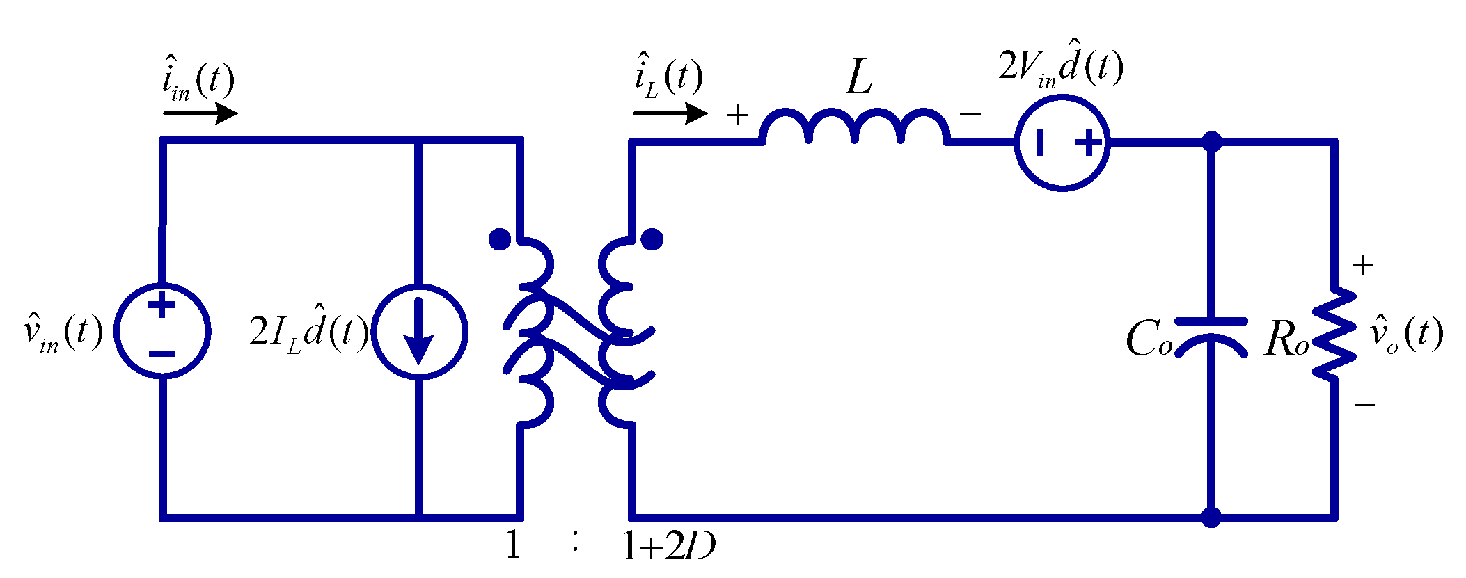
2.6. Transfer Function and Control Design
The adopted modeling technique is based on the basic AC modeling approach proposed in [
30]. In this regard, aiming to obtain the small-signal AC equivalent circuit, as shown in
Figure 5, small-signal perturbations are applied around the equilibrium point, and its frequency response is validated by the AC sweep analysis performed in PSIM® software (UNESP, Ilha Solteira, Brazil), as shown in
Figure 6a. From that circuit, the control-to-output
and line-to-output
transfer functions are obtained and are described by (
34) and (
35), respectively.
By analyzing the transfer function
, the proposed converter behaves as a minimum-phase system, due to the absence of right-half-plane (RHP) zeros. Therefore, the controller design process is simplified for the 3SSC-A-based boost converter and the problems associated with right-half-plane (RHP) zeros are eliminated. Thus, it is possible to obtain a satisfactory dynamic response without implementing an additional control loop. Moreover, it is observed that the dynamic characteristics are similar to the classic buck converter operating in CCM, which can be mathematically evidenced by the transfer function expressed in (
35). It differs from the transfer function of the boost 3SSC-B-based converter presented in [
31], which has characteristics like the classic boost converter.
In this regard, by using the design specifications from
Table 1, the bode diagram of the transfer function
, including the gain sensor
V/V, is illustrated in
Figure 6b (blue curve). The average voltage-mode control technique is applied to the regulation of the output voltage of the converter and, due to the characteristic of the control-to-output transfer function, the PI controller was adopted. The conventional phase-margin and gain-margin stability criteria are applied, where a crossing frequency is around 1/4 and 1/10 of the switching frequency, and a phase margin 45° ≤ PM ≤ 90° should be attended to provide a good response with an adequate output-voltage overshoot. As shown in
Figure 6 (red in color), by using a proportional gain
= 0.1033 and an integral gain
= 7944 for the controller PI, the crossover frequency and phase margin obtained from the voltage control loop are 5 kHz and 90°, respectively.
3. Comparison with Other Boost Converter Topologies
Table 2 summarizes the main characteristics of the 3SSC-A-based boost converter compared to other structures with current source characteristics at the output and RHP zero free control-to-output transfer function. It is observed that the first-order KY converter has the lowest number of semiconductors, however, it has the same number of controlled switches as the 3SSC-A-based boost converter. On the other hand, since the controlled switches are in the same reference, the command scheme of the 3SSC-A-based boost could result in simpler circuits. The interleaved tri-state boost converter exhibits the largest number of semiconductors, requiring greater complexity in the command and control scheme among the aforementioned topologies. With regard to voltage stress, the first-order KY converter presents the least stress on the switches.
The 3SSC-A-based boost converter is the only one that uses an autotransformer, with a turn ratio equal to unity, which guarantees the distribution of current stress in the semiconductors. In addition, all the energy storage elements of this structure operate at twice the switching frequency, which provides a reduction in weight and volume compared to other topologies. In addition, the interleaved tri-state boost has a high voltage gain compared to other converters, however, its static gain has a nonlinear behavior and is dependent on the possible switching logic of this structure. It is important to remark that, although 3SSC-A-based boost operates with duty cycle less than 0.5, the maximum static gain is equal to the 1st-order KY converter.
4. Experimental Results
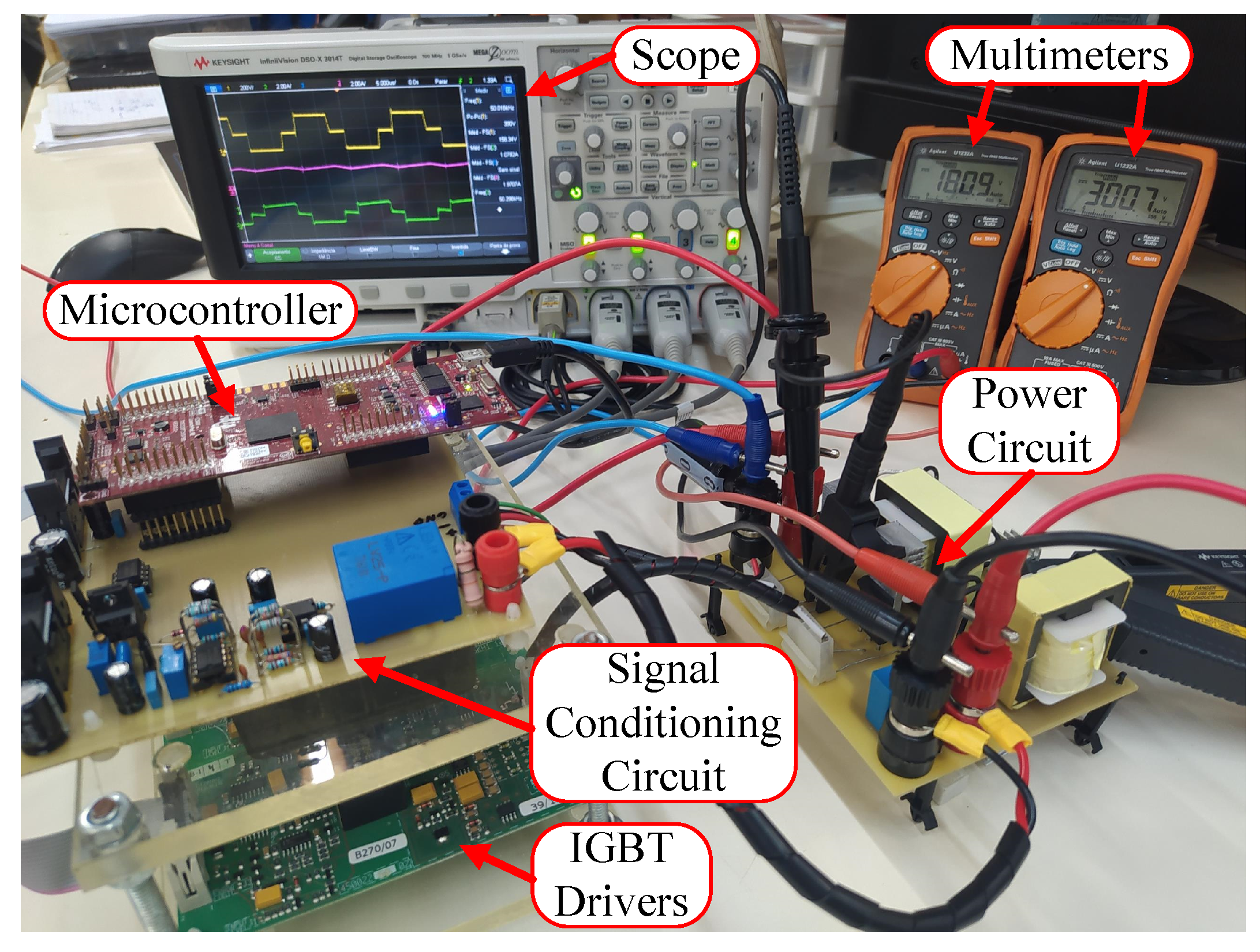
The experimental set-up implemented to carry out the laboratory tests is shown in
Figure 7. The power circuit of the 3SSC-A-based boost converter was assembled according to the parameters presented in
Table 1. It is noteworthy that, by applying the methodology presented in
Section 2 for the autotransformer design, the NEE-30/15/14 core was found, however, due to the available components at the laboratory, the NEE-42/21/20 core was used.
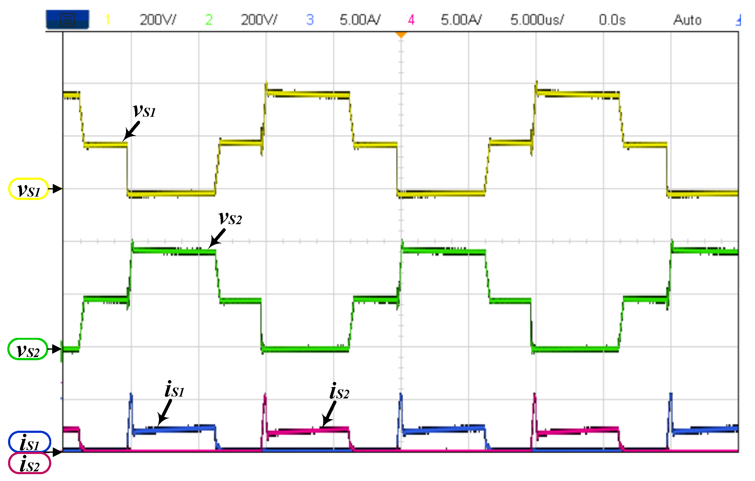
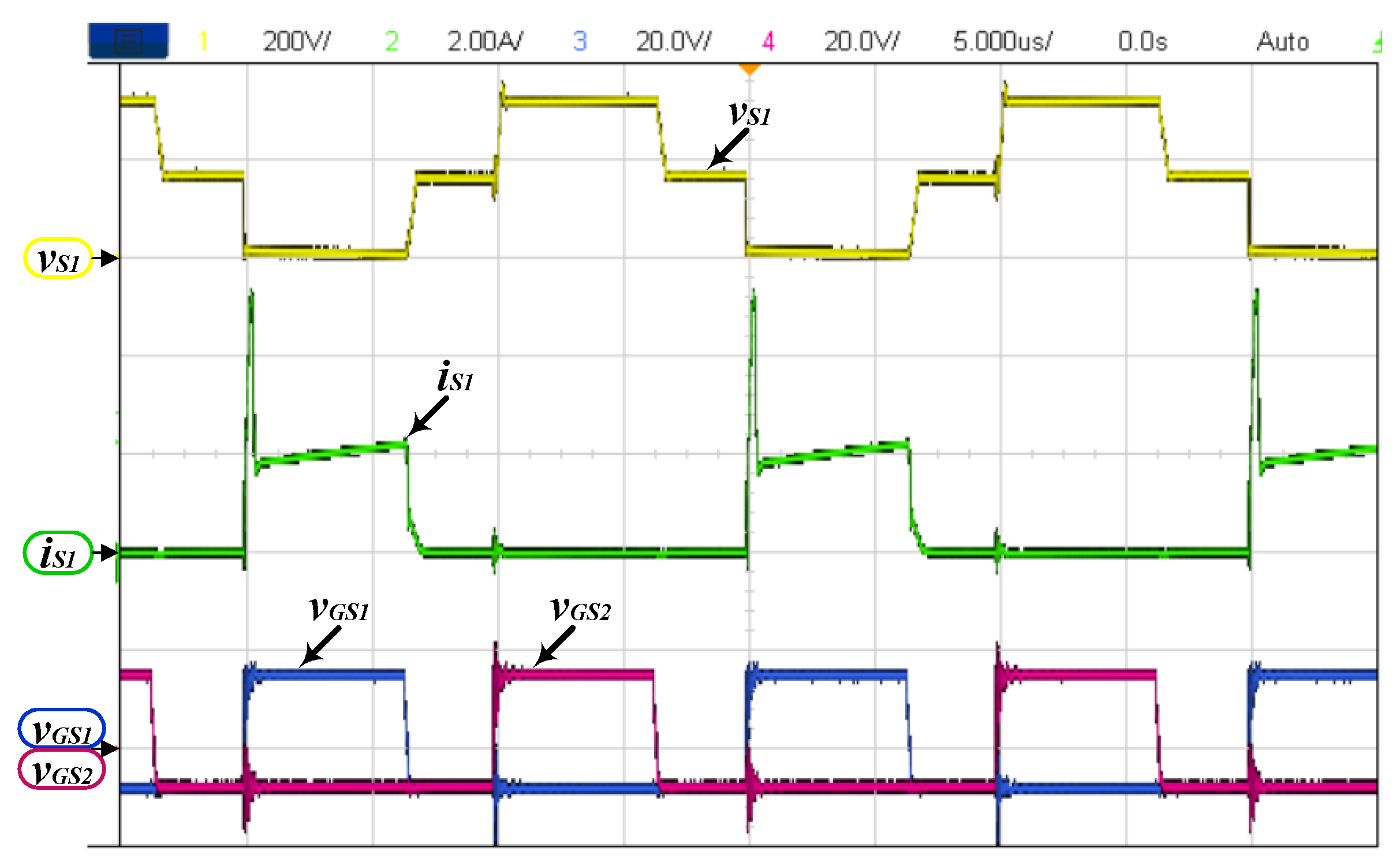
Figure 8 shows the control signals of the switches
and
, demonstrating that the converter operates without overlapping of the pulses, with D = 0.33. Additionally, it is illustrated the maximum voltage of the
is approximately 360 V. The current
increases linearly being approximately 2.2 A. The waveforms related to the voltage and current stress on the switches
and
are shown in
Figure 9. It is observed that the switches do not remain turned on simultaneously, with a 180-degree delay between the command signals being evident. It is worth remarking that the interaction between the autotransformer leakage inductance and the IGBT collector–emitter capacitance results in an equivalent resonant LC circuit in the activation process, which causes the current spikes seen in the currents
and
in
Figure 9. Moreover, the leakage inductance would also cause voltage spikes on switches, however, these spikes were reduced by using RLD snubber circuits. Additionally, the effect of the autotransformer windings leakage inductance could be alleviated by increasing the coupling factor, which can be achieved by replacing the EE core with a toroidal core, increasing the occupation of the window area, and applying suitable interleaved winding techniques [
32].
In
Figure 10, the voltage
, the current
, and the currents
e
are illustrated. The maximum reverse voltage on the diodes is equivalent to
−360 V, according to the theoretical analysis. Looking at the currents
and
, it can be verified that the switch
and the diode
do not operate simultaneously, validating the complement operation between these semiconductors. Furthermore, it can be observed, from the current
’s behavior, that the converter operates in CCM, and the frequency of the ripple current
is equal to 100 kHz, corresponding to twice the switching frequency, with an average value of 2 A. Moreover, it can be seen the diodes
and
conduct simultaneously when the current
decreases linearly, i.e., the moment when the switches
and
are turned off, and the current through each diode is equivalent to half of the current
, with an average value of 1 A.
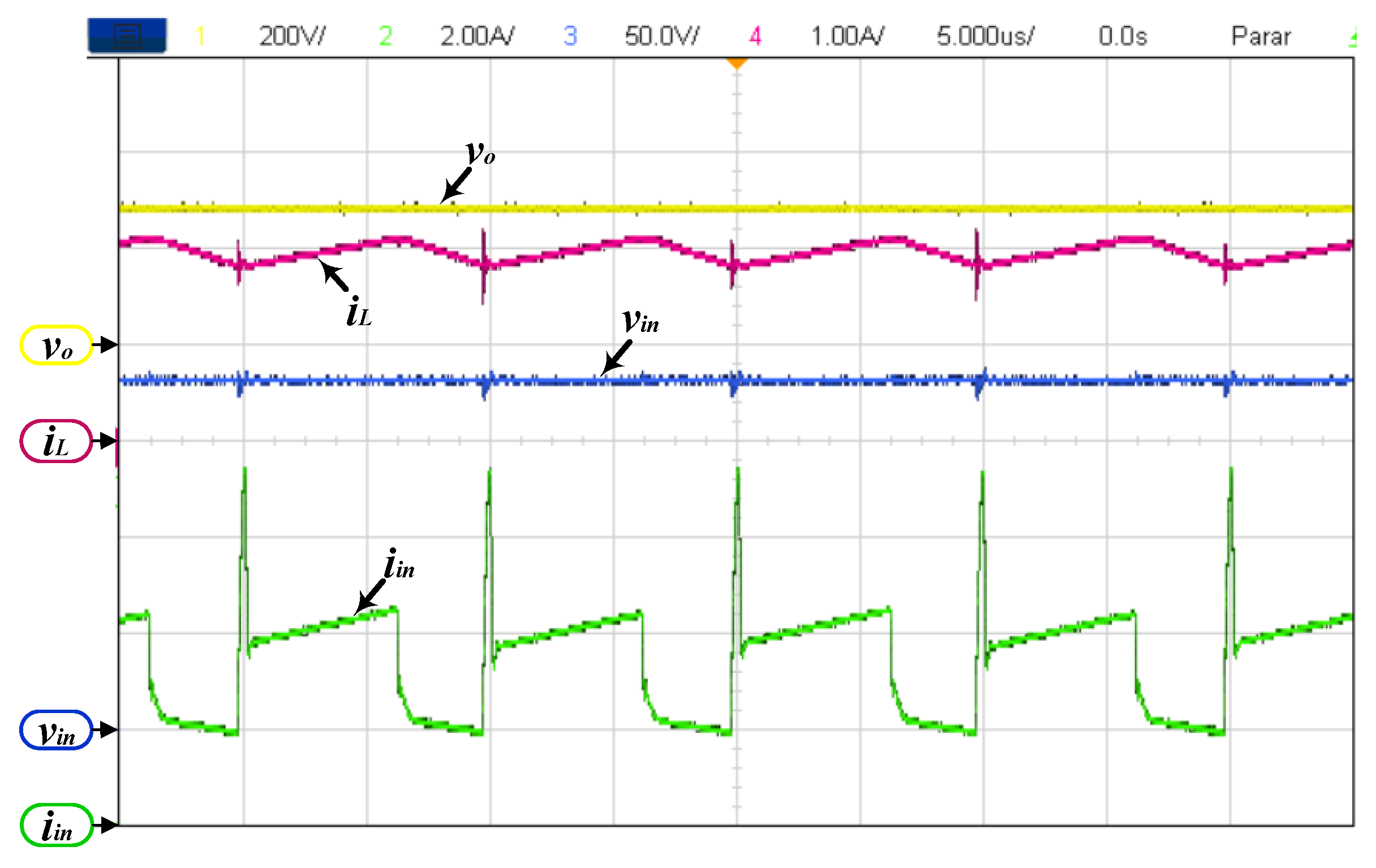
Figure 11 shows the waveforms of the voltage
, the voltage
, the current
, and the input current
. These results evidence that the converter operates as step-up structure, with
equal to 300 V, corresponding to the gain required. It is verified that the current
presents a greater ripple than the current
and its shape shows the characteristic of the voltage-fed converter, in contrast to the classic boost converter and the 3SSC-B-based boost topology, which present current-fed converter characteristic.
The dynamic responses of
,
, and
, during a load variation, are shown in
Figure 12. Initially, at
t = 400 ms the load decrease from 600 W to 300 W, and then, at
t = 1250 ms, the load is increased from 300 W to 600 W. It can be verified an output-voltage overshoot lower than 6% of the rated voltage.
According to the loss model described in
Section 2.2 and
Table 2, the distribution of theoretical power losses in the converter, operating at full load, is shown in
Figure 13, which is equivalent to the total theoretical power losses of 17.2 W and theoretical efficiency of around 97.2%. It is observed that semiconductors are the elements that most contribute to total losses, and the power losses in magnetic elements are mainly given by the cooper losses. Moreover, due to the low current ripple and the small ESR, it can be noted that the power losses in the capacitor are extremely reduced when compared to the other elements. The efficiency of the experimental prototype was evaluated in a load range of 100 W to 600 W, as shown in
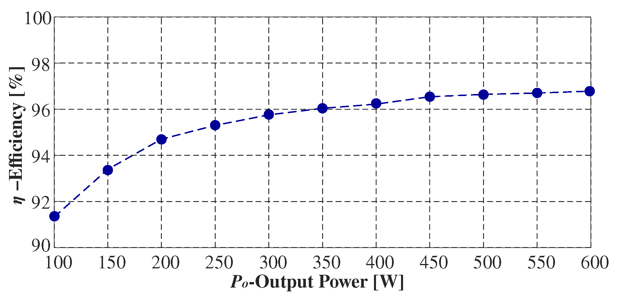
Figure 14. It is verified that the performance of the prototype is greater than 91% in the whole range of defined power, at nominal load this is approximately 96.8%.
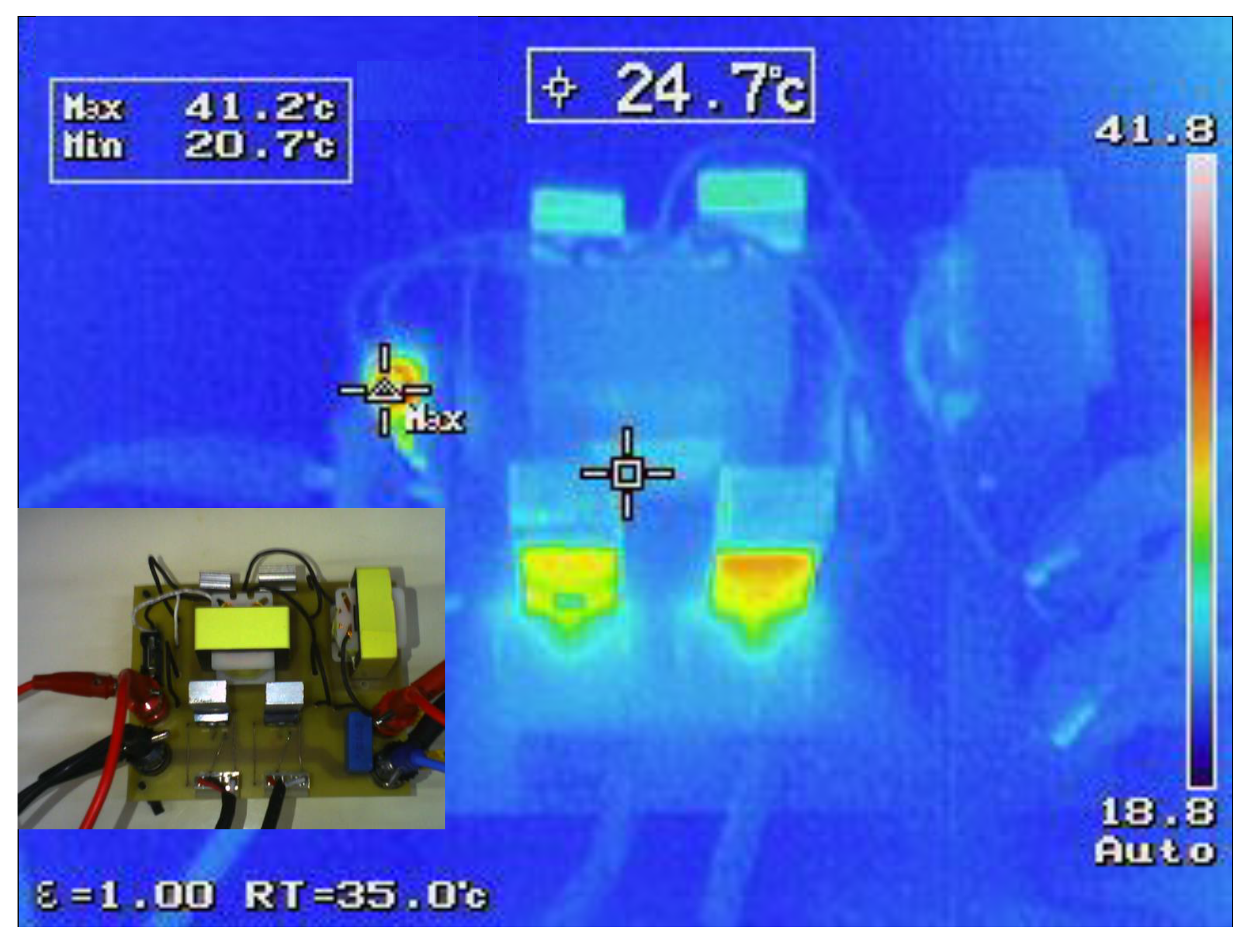
In nominal power conditions, the thermal distribution in the converter is evaluated by means of a thermal imaging camera, as presented in
Figure 15. Due to the current division between these components, the distribution of thermal losses between the semiconductors, which is related to the operating characteristic of the 3SSC-A. At full load, the maximum component temperature is less than 45 °C.
5. Conclusions
This paper presented the 3SSC-A-based boost converter, filling a gap in the literature, regarding the complete study of this topology. The incorporation of the type-A 3SSC structure results in advantageous characteristics compared to the classic boost converters, offering a low-ripple in the current of the output capacitor, which reduces the losses due to the capacitor’s series resistance and, consequently, increases the useful life of this element.
Through the study of the converter dynamics, it was found that, unlike classic boost topologies, the control-to-output transfer function of the 3SSC-A-based boost has a minimum-phase characteristic, which allows the use of only one control-loop, with a simple controller, offering fast load transient responses, similar to the classic buck converter behavior. Besides, the high-level efficiency, the 3SSC-A-based boost converter presents the typical advantages related to 3SSC, such as weight and volume reduction of passive components, division of the current stress between semiconductors and losses thermal distribution, providing reducing the size of the heat sinks.
The 3SSC-A-based boost converter becomes an attractive solution for step-up structures that require to supply of critical loads sensitive with low current ripple. Furthermore, the use of the structure in several energy conditioning applications that require high performance and high power density could be explored.


 and
and 


