1. Introduction
Voltage source inverters (VSI) produce a sinusoidal voltage of desired phase and magnitude using PWM techniques. Multilevel voltage source inverters (MLIs) have emerged as feasible solutions to improve the performance of renewable energy systems (RES), grid integration, electric vehicles, uninterruptible power supplies (UPS) and other state of the art power electronics utilities [
1,
2]. These converters can generate output voltages of the better harmonic spectrum and reduced THD levels through appropriate switching [
3]. The conventional multilevel inverters are the neutral point clamped multilevel inverter (NPC-MLI) [
4], cascaded H bridge inverter and flying capacitor multilevel inverter (FC-MLI). With the increase in the output voltage levels count, a number of the flying capacitors in FC-MLI, the number of the clamping diodes in NPC-MLI and the number of isolated DC sources in CHB-MLI increases considerably. Moreover, FC and NPC converters require additional circuit and sophisticated algorithms to maintain the voltage balance across the capacitors.
Furthermore, load end transformers or DC-DC converters are also required to obtain the high value of AC voltage. All of these requirements make the inverter more complex, large and costly. To overcome the drawbacks of traditional topologies, switched capacitor based multilevel inverters are presented in [
5,
6,
7,
8,
9,
10,
11]. These topologies aim to reduce the DC source count and number of active switches. In this work, a recently introduced 13-level WE type inverter [
12], a switched capacitor multilevel inverter, is explored for hysteresis control with the 12-band operation. This topology was also introduced as a 9-level topology in [
13]. The bands are decided by applying the genetic algorithm (GA), and the balancing of the DC link is maintained by using redundant states. By choosing the proper switching sequence and charging and discharging paths, capacitor voltage balancing is achieved. A single sensor is required across the DC link to operate in closed-loop control [
14]. High quality stabilized load voltage is required by industrial applications. The performance and operation of multilevel inverters depend on the type of control strategy [
15]. Various control techniques are used in multilevel inverters such as conventional pulse width modulation (PWM), hysteresis control, sliding mode control techniques and modern predictive control. Current control techniques for conventional inverters have been discussed in [
15,
16].
Hysteresis current control technique is employed in [
17] for multilevel inverters. In [
17], although a constant switching frequency is achieved, implementation is complex, and in [
18], another method with variable switching frequency and ease in implementation is achieved. The hysteresis current control technique has a major challenge of selecting the number of levels to limit the current error to the hysteresis bands [
19]. One strategy is time-based lockout which will repetitively limit the current error in the bounds. Another approach is using multiple bands to control the current error [
20]. This type of control is also discussed in [
21,
22,
23]. Different types of hysteresis control such as multiband, multi offset band and time-based multi offset band controls are used in [
24]. These methods are widely applicable to the topologies that have inherited capacitor balancing. Still, if the external capacitor balancing is required, then an additional proportional integrator (PI) control loop is required to balance the capacitors and generate the desired current error reference [
25].
Tuning PI control parameters is cumbersome and various difficulties such as non-linearities, time delays and higher-order systems make it time-consuming and less precise. Over the past few years, heuristic methods have been proposed to solve the problem of tuning. Ziegler–Nichols is one of the classical methods, but it is hard to find the optimal parameters in industrial power converters. Therefore, the capability of the PI tuning method has to be increased by adding more features. Many AI techniques are used in tunings, such as neural networks, fuzzy neural logic [
26] and fuzzy system, to find the optimal value of PI constants. Nature inspired techniques such as genetic algorithm (GA) [
27,
28], particles swarm optimization (PSO) [
29], bee algorithm (BA) [
30] and bat algorithm (BAT) [
31] have gained interest in achieving high efficiency and finding an optimal solution to the problem [
32].
In this paper, a new GA based PI-controlled 12-band hysteresis current control is applied on WE topology. The 13-level WE type inverter topology and its switching states are described in
Section 2.
Section 3 discusses the implementation of 12-band hysteresis control of the WE inverter topology with the GA for tuning the PI controller and the conventional Ziegler–Nichols method, along with their comparative analysis.
Section 4 shows and analyzes simulation results with different hysteresis bandwidth (
h), load conditions and tuning methods. In
Section 5, experimental results are presented and discussed, and
Section 6 concludes and summarizes the paper.
2. WE Topology Circuit Description and Operation
Proposed 12-band hysteresis control is tested on a 13-level inverter topology resembling the English letters “WE”. This topology generates 13 levels at the load voltage.
Figure 1 illustrates the circuit of the 13-level WE-type inverter topology. The arrangements consist of a DC source that forms the main DC link, two capacitors forming the auxiliary DC link, nine insulated gate bipolar junction transistors (IGBTs) and one anti-parallel connected AC switch. The switches S
1, S
2, S
3, S
1′, S
2′, S
3′ and S
4 form a W and S
5, S
5′ and the AC switch S
6 form the letter E, hence the name WE-type inverter. With a single DC source in its main DC link, this topology is capable of producing 1.5 times boosted output voltage. The switches S
1 and S
1′, S
2 and S
2′, S
3 and S
3′ and also S
5, S
5′ and S
6 perform in a complimentary fashion. As persistent with the asymmetrical topologies, the switches of this topology are also subjected to different voltage stresses and operational frequencies. The circuit configuration suggests that the upper switches of the converter will block higher voltage and operate at low frequency, while the lower switches will block a lower voltage and operate at high frequency compared to the upper switches.
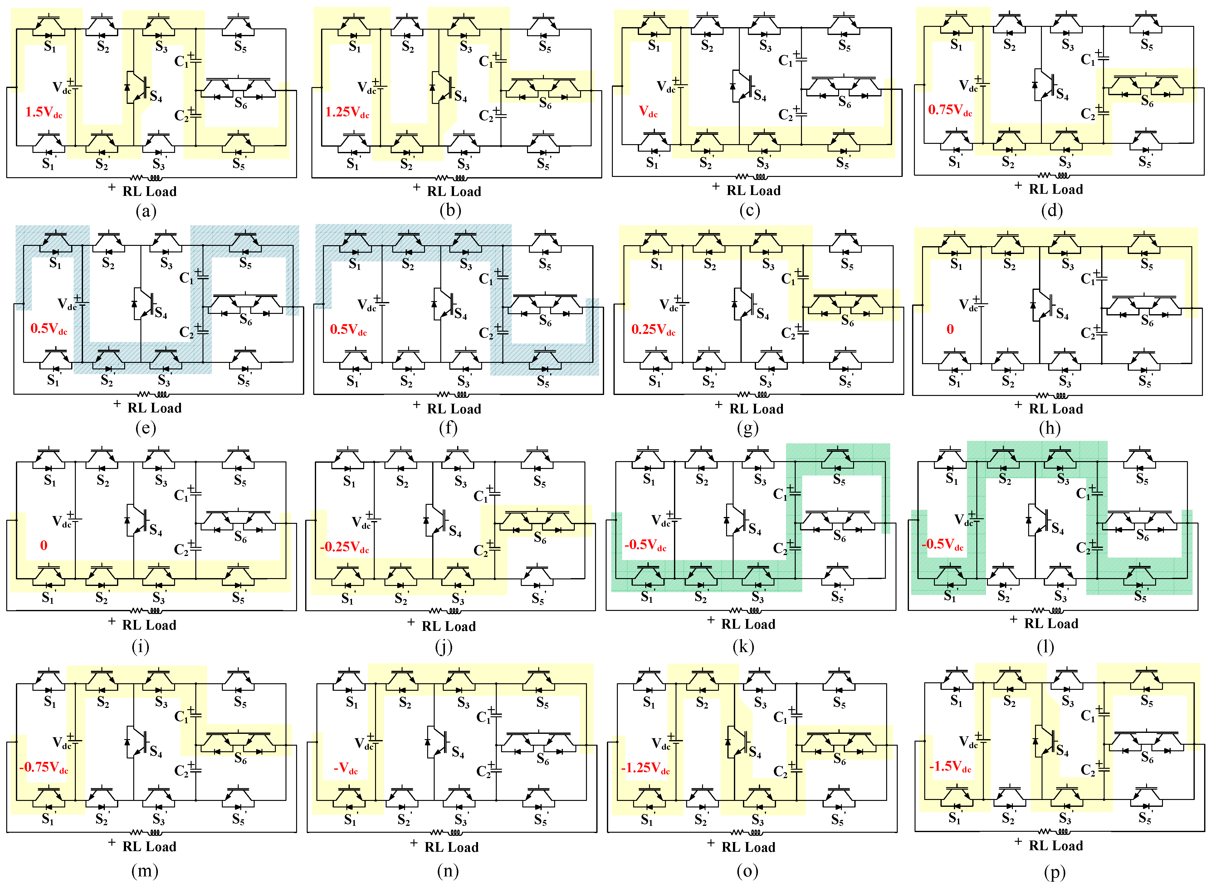
Figure 2 exhibits all the possible sixteen states of the converter. Each subfigure highlights the conduction path and the current flow from left to right in the load is the positive current. The states also explain the charging and discharging conditions of the capacitors with current directions in
Table 1.
If S
f1, S
f1′, S
f2, S
f2′, S
f3, S
f3′, S
f4, S
f5, S
f5′ and S
f6 represent the switching functions of S
1, S
1′, S
2, S
2′, S
3, S
3′, S
4, S
5, S
5′ and S
6, the output voltage of the converter that represents all the states can be derived as follows. Each switching function will have a value as follows:
The output voltage ex.
The output voltage expression in the preliminary form as:
where, the terms can be defined as follows:
Equations (4)–(6) and the following auxiliary DC-link equation will lead to all the possible states presented in the diagrams of
Figure 2 and in
Table 1.
3. Hysteresis Control for WE Topology
Hysteresis current control technique works on the principle of regulating the current error (e
i) within the multiple bands. The number of bands is (
n − 1) where
n = number of levels generated by the inverter. The type of hysteresis modulation used in WE topology is the multiband hysteresis current control technique. This technique enjoys various advantages such as a good dynamic response and stable operation [
20]. However, this technique is prone to noise in the current error [
23]. In this technique, the current error is closely checked within limits decided by hysteresis band ‘h’. The efficacy of hysteresis band control is proved to be an efficient and stable control, especially for topologies having inherited balancing capability. However, in the last few years, hysteresis control is being applied on topologies that do not have inherent capacitor balancing by using additional PI controllers. These controllers’ parameters K
p and K
i are tuned to generate the current reference from voltage error across the capacitors. However, the tuning of the PI controller is a very hard and time-consuming task because of the complexity and nonlinearity in control [
15]. Therefore, there is always a need to find the precise K
p and Ki values. A different nature inspired heuristic approach is taken into consideration to find the constants of the PI controller. One widely available is the genetic algorithm in [
26]. In this paper, PI constants are found using the Ziegler–Nichols method and the genetic algorithm.
3.1. Implementation of 12-Band Hysteresis Control
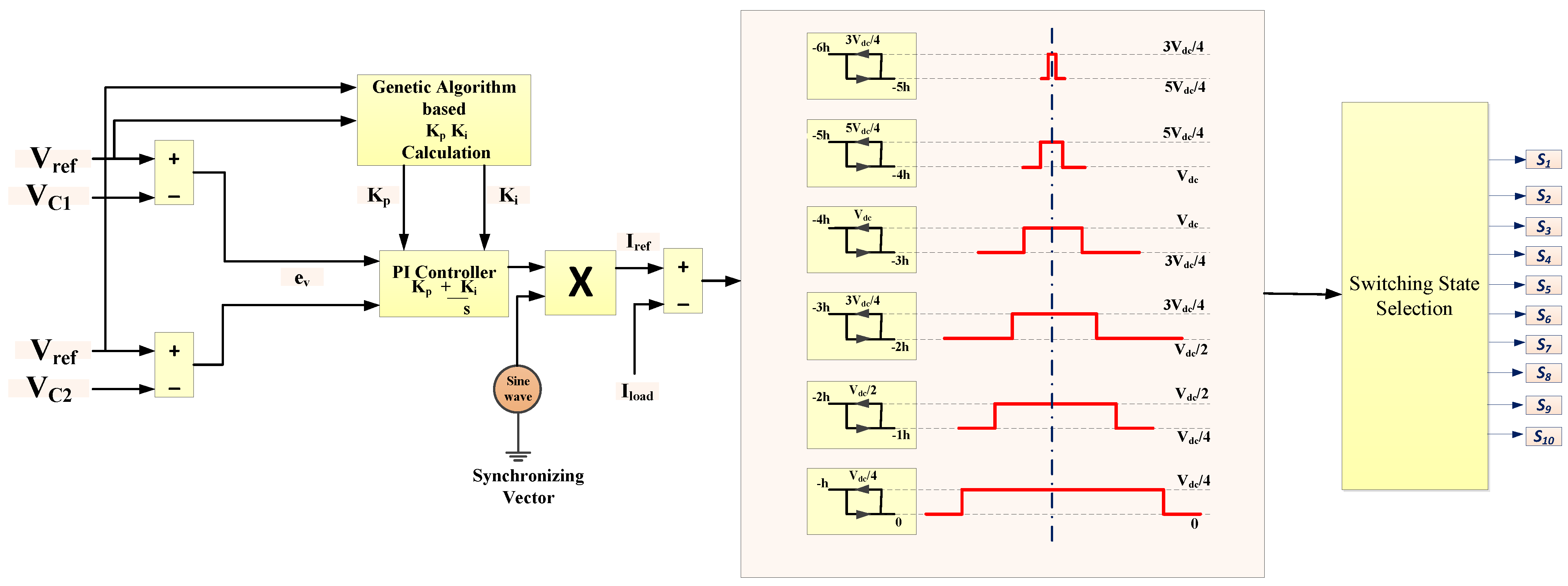
In hysteresis current control, gate signals are switched to force the load current to follow the current reference value within the predefined hysteresis bands. The multiband hysteresis control technique uses n − 1 bands for the n level inverter to limit the current error and generate an n-level load voltage. So, for 13-levels 12 bands are needed in this technique. These bands are made by two parameters that are load voltage levels (multiple of source voltage Vdc) and current error ∆i. Upper bands generate the positive cycle and lower bands generate the negative cycle of the load voltage.
In
Figure 3, complete control flow is shown. The voltages across the capacitors are sensed and compared with the set reference value of voltage that is to be maintained across the capacitors. To balance this link capacitor voltage and generate the reference current in proportion to their required value of load current K
p and K
i value of the PI controller is found. In the next stage, the output of the PI controller is then multiplied by synchronizing vector to match the power frequency of load voltage. The output of the multiplier generates the output signal equal to the reference current in accordance to load current. The reference and load current are subtracted and the current error is generated, which is of the same frequency and phase as load voltage.
The error signal is then given to the hysteresis block. As the voltage increases, the current has to change the direction to keep itself in the band limit. The error may reach the next boundary if it has not changed the direction. If the error passes, the band limits the inverter switches to the next voltage level. Twelve bands (0→−h) (−h→−2 h) (−2 h→−3 h) (−3 h→−4 h) (−4 h→−5 h) (−5 h→−6 h) and (0→h) (h→2 h) (2 h→3 h) (3 h→4 h) (4 h→ 5 h) (5 h→6 h) have the bandwidth ‘h’
of about 2% to 5% of rated load current. For achieving the load voltage of 13 level, the capacitor voltage has to be maintained to Vdc/4. The current error is quantified into 12 bands of bandwidth ‘h’. The variation of error leads to transitions among the different voltage levels. Further, the switching states are selected according to the transitions, and the gate signal is triggered.
3.2. Heuristic Based PI Control
The PI controller generates the required current error in the hysteresis band control. The optimal tuning of the gain constants, namely proportional and integral gains (Kp and Ki), is difficult. This paper employs a nature based and evolution rooted genetic algorithm (GA) to find the best possible values of these gain constants in minimum time duration. These techniques provide the fine-tuning of weighting factors for PI controllers and acquire the global optimum solutions [
13,
14]. The most striking feature of this method is that it avoids the early settlement to the suboptimal search space and has very fast convergence with a reduction in the inaccuracies and uncertainties in obtaining the global optimum solution in the region of search space [
15,
16]. The merits of a GA-tuned PI controller over the conventional PI controller are as follows:
The searching of the points in a parallel manner provides a much wider region of search space as compared to the single point search, which is carried out usually in the PI controller.
The direction of the search space is affected only by objective function and fitness level and independent of the PI controller’s extra integral data.
It employs the probabilistic transition rule rather than deterministic.
The GA based PI controllers are applied in relevant process control industries because they handle the processes with dynamic parameters, non-linear constraints and multiple objectives [
26].
3.3. Ziegler–Nichols Method
The Ziegler–Nichols method is a heuristic method used to tune the PI controller. This method is employed by taking the values of integral and derivative gains equal to zero. The proportional gain (Kp) is then allowed to increase until a gain is reached where the control loop output starts oscillating with constant amplitude. The Ziegler–Nichols method has a limitation that it can be applied to tune the processes that run in a closed-loop only. Determination of the definitive gain value is achieved by only finding the value of the proportional gain that results in the indefinite oscillation of the loop at steady state. This states that the gain obtained from the derivative and integral controller are set to zero so that the effect of proportional gain can be determined. One more important value linked with this proportional only method of control tuning is the ultimate period. This period is the time required to complete a complete oscillation while the system is at steady state. These two parameters are used to find the loop tuning constants of the PI controller.
3.4. Genetic Algorithm
Metaheuristic-based algorithms exhibited their effectiveness in solving the real-world problems requiring optimization that are non-linear in nature and their convergence with the traditional techniques are either tedious or do not occur at all. Evolutionary techniques inspired by nature have evolved and are applied in a multitude of optimization applications. In this paper, genetic algorithm (GA) [
26,
27] is employed to find the values of the gain constants (K
p and K
i) of the PI controller that ultimately balances the voltage across the capacitors, which is a condition to generate 13 levels at the output. Moreover, the appropriate value of gain constant reflects in the minimization of the overall THD in the output voltage. The most striking features of the GA are:
The various steps involved in the application of the GA are discussed in this sub-section and is further explained with the help of a flow chart.
3.4.1. Design Variables
The design variables of the GA are generally represented in the form of binary strings of 0 and 1 to facilitate the digital signal processing. The initial population is selected in a purely random manner. The weighted constants k
1, k
3, ⋯, k
49 are such defined that k
1 > k
3 >⋯> k
24, with k
1 = 1000. The first eight bits are allocated to first design variables, which are obtained by linking the strings end to end, with the next eight bits to second design variable and so on. In order to satisfy the dependent limits on design variables for the problem, the total harmonic distortion is calculated by:
3.4.2. Selection
In this step, the selection of the two parents is being carried out purely on the probabilistic basis. Roulette wheel criteria-based approach is being applied. The random selection of parents ensures a thorough exploration of selection domain. This also get reflected in the results as a sudden surge, as shown in
Figure 4.
3.4.3. Crossover
In this step, the intermixing of the genes in a particular way takes place. In this work, the process of the formation of the child’s chromosomes takes place in such a manner that half of the bits are taken from one parent and the other half from the spouse. The process of intermixing repeats for all 24 bytes of the chromosomes is shown in
Figure 4. There are
N numbers of the children produced, where ε is the current child as depicted in the flowchart in
Figure 5.
3.4.4. Mutation
The process of the improvement in the various traits of offspring compared to the parent characteristics is known as mutation. This mutation process is incorporated in the genetic algorithm by the flipping of the values in the bits. In this way, every bit of each byte of the offspring’s chromosome is altered. Furthermore, it ensures that some of the children inherit the same characteristics from parents and the whole children population is not mutated. Instead, a random number λ is generated and, in case the value of λ is less than a fixed number M, then only the mutation of offspring will take place.
The efficacy of the GA over other nature inspired techniques such as bee and bat algorithms can be seen in
Figure 6.The fitness function in terms of minimum THD is used for checking the applicability and getting the faster response from the PI controller. From the figure it is clearly seen that the convergence of the GA is faster than bee and bat algorithm-based PI controllers.
3.5. Application of Genetic Algorithm
Output THD depends on the value of the fundamental component and magnitude of harmonics.
This equation is being treated as the objective function for the application of nature inspired technique based genetic algorithm (GA). The AC load voltage reference can be generated by the below mentioned equation:
where
is load current reference.
As the RMS value of the output voltage is the function of the voltage across the capacitors and it is required to maintain 0.25 Vin (i.e., one fourth of the applied DC voltage) and output current is a function of gain constants. The voltage across the capacitors is controlled by employing the PI controller such that
= , and are capacitor voltage references.
Constrained involved (when 100 V DC source voltage is applied):
Equation (4) is considered as the fitness function. The PI controller starts with the randomly selected values from the initial population, capacitor voltage takes place according to these selected values of gain constants. The values of the gain constants obtained by following genetic algorithm influences the voltage balancing across the capacitors. This ultimately influences the total harmonic distortion (THD) of the output voltage, the steps involved in the application of the GA for searching the most appropriate values for the PI controller to obtain the voltage balancing across the capacitors and for minimum value of the THD, which are depicted by a flow chart in Figure.
4. Simulation Results and Analysis
Simulations were performed on MATLAB Simulink for testing the proposed control.
Figure 7a exhibits the output voltage and current waveforms of the 13-level WE topology. These results are obtained at
h = 0.03 and the PI constants value is found by the GA based controller. The parameters of simulation are shown in
Table 2. The PI constants values calculated are 0.01 and 0.0299, respectively. It is observed that the voltage and current waveforms are found to be in phase with each other and the power factor is approximately unity. The inverter’s output voltage gets boosted to 1.5 times the DC source voltage at the input side.
Figure 7b,c presents the harmonic analysis of the output current and voltage waveform. It is observed that the harmonic components appearing in the lower frequency range are less compared to higher order harmonic, which can be easily filtered out. The THD of the output voltage and output current at
h = 0.03 is 4.76% and 0.83%, respectively. A performance comparison of the above results with the conventional ZN method and GA based control is shown in
Figure 8; for low
h values the response with ZN is slower and oscillatory than for GA. For
h = 0.002 and
h = −0.03, the DC link voltage has been stabilized much earlier and faster at PI constants values calculated from ZN. Overall, it can be seen that the genetic algorithm-based control has given values of K
p and K
i much more precise and exact, which stabilizes the DC link voltage much earlier than values calculated from ZN. The variation in the average switching frequency and THD of the load current with the hysteresis band control and its evolution is shown in
Figure 9a.The main issue faced with the application of hysteresis control is the irregularity in the switching frequency of the inverter. Nonetheless, on increasing the hysteresis bandwidth (
h), this anomalous behavior can be limited, which deteriorates the current THD. The secondary DC bus remains well regulated. The regulator gains obtained by applying the nature inspired GA algorithm are 0.01 and 0.0299 for proportional and integral action, respectively. In some applications, the hysteresis band is limited to some small values and should not exceed a limit, and it is not possible to limit the switching frequency and the THD of the load current after applying hysteresis band control, as shown in
Figure 9a. Several solutions were also proposed in literature, such as the use of constant switching frequency described in [
29,
30]. In
Figure 9b, the THD of the output voltage decreases sharply when the hysteresis bandwidth (
h) decreases from 0.01 to 0.03, reaches a minimum value of 4.64% at
h = 0.03 and, again with the increase in
h, the THD value increases slightly. Similarly, the value of current
THD also experienced a sharp decrease in the THD level initially and then a slight increase with the increasing
h is noticed.
Total harmonic distortion percentage of voltage and current with varying load have been shown in
Figure 10a at hysteresis bandwidth of 0.03. THD percentage values are lower for low load values and increasing as the load is increased in both load voltage and load current. In
Figure 10b, DC link capacitor voltage has been shown for four different hysteresis band values, that is
h = 0.01,
h = 0.03,
h = 0.02 and
h = 0.04. The response has been shown when the K
p and K
i values are calculated from both genetic algorithm and Ziegler–Nichols method. One of the parameters that is also important for proper generation of voltage levels is DC link voltage which is maintained by balancing capacitor voltage to 25 volts each. In addition, for this it is necessary to analyze the effect of load voltage and hysteresis bandwidth variation. For high load value, the capacitor ripple percentage is also high and among the maximum at
h = 0.01. For medium load at 50 ohm, 40 mH, there is an overall dip in the ripple percentage, especially at
h = 0.04. In the case of load value, the capacitor ripple is less and minimum at
h = 0.03.
5. Experimental Results
A 200 V-600 W experimental prototype has been designed to check the operability and confirm the simulation results for WE-type thirteen-level inverter controlled by 12-band hysteresis control using a GA based PI controller. The output frequency and switching frequencies selected are 50 Hz and 5000 Hz, respectively. The maximum input voltage is 100 Volts. Experimental setup has been shown in
Figure 11. The gate pulses are generated by Texas DSP TMS320F28379D, and the dead time was taken as 5 microseconds. Further, a real-time validation is also performed using a Typhoon HIL emulator. In
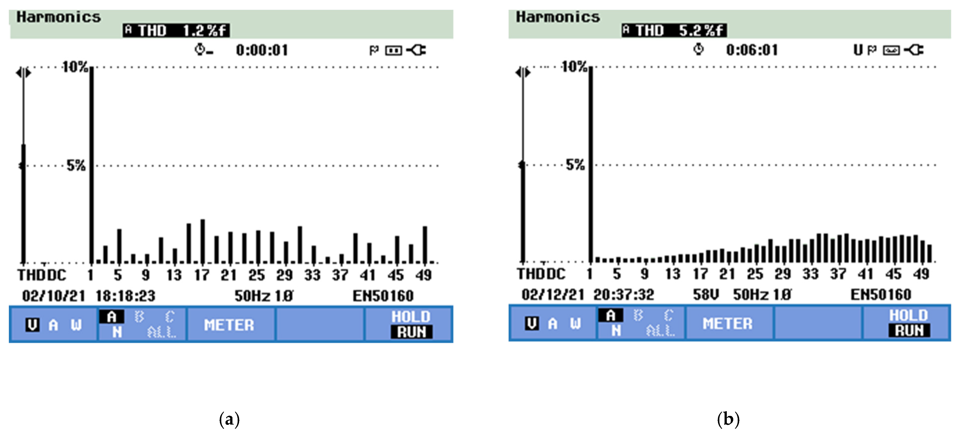
Figure 12, thirteen-level output voltage with load current and DC link voltage is shown, which clearly confirms the voltage boosting capability. The input voltage taken is 100 Volts and output peak voltage is 150 Volts. The efficiency of the inverter is around 94% at rated power output on AC load. Frequency spectrums for load voltage and current at
h = 0.03 have been shown in
Figure 13, which are very close to the simulated results. Output voltage and current for three different hysteresis bandwidths (
h) are shown in
Figure 14. The load taken is 120 Ω and 40 mH. To show the satisfactory operation of WE-type topology using 12-band hysteresis control, two different types of conditions are created and response of prototype is observed. In
Figure 15a, load voltage and current with voltage across C
1 is shown when the load impedance is varied in three stages. The waveforms clearly show that while varying the load impedance, the load voltage waveforms are not affected and voltage balancing across the DC link is done by varying the proportional constants (K
p and K
i) using a real-time GA based PI controller. Operation of inverter under variable DC source voltage has been shown in
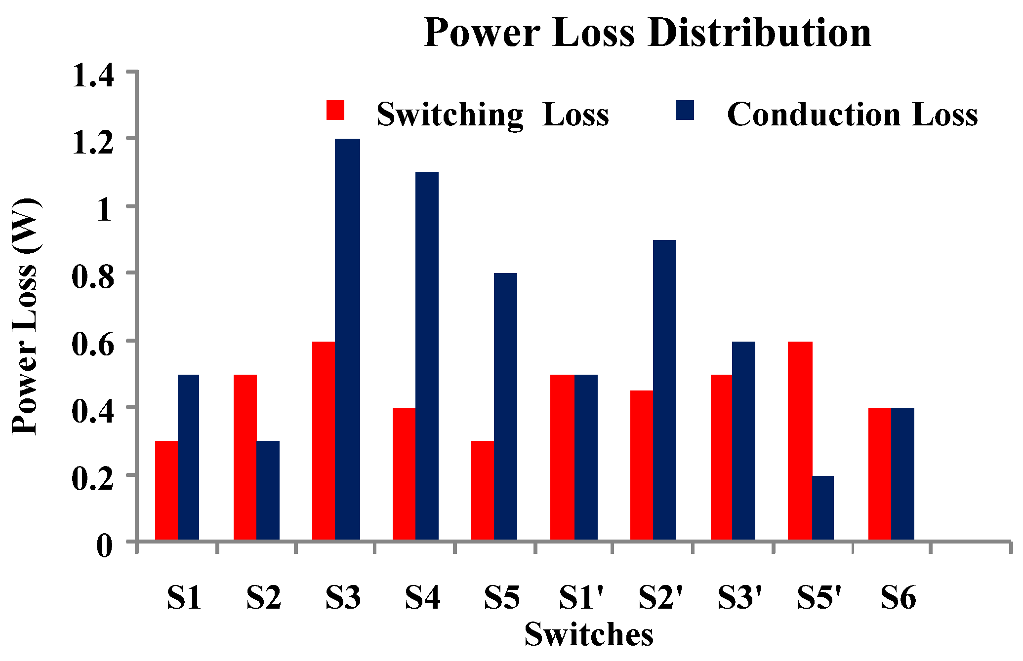
Figure 15b. Three different DC source voltages, 70 volts, 100 Volts and 20 Volts, are taken and constant load of 130 Ω and 40 mH is applied. The DC link is well regulated and output load voltage and current are clearly defined. Power loss analysis has been done by PLECS Simulation software and also verified on actual hardware. Loss breakup across the switches is shown in
Figure 16. Experimental prototype of 200 V-300 W is used to validate the loss calculations. Total loss calculated by PLECS is ~9 W and on hardware is ~10 W.


 ,
, 


