Article

Synthesis of Antennas for Active Glazing Unit with Photovoltaic Modules

by
Piotr Jankowski-Mihułowicz
1,*,
Mariusz Węglarski
1,*,
Wojciech Lichoń
2,
Mateusz Chamera
2,
Patryk Pyt
1 and
Cezary Ciejka
3
1
Department of Electronic and Telecommunications Systems, Rzeszów University of Technology, ul. Wincentego Pola 2, 35-959 Rzeszów, Poland
2
Talkin’ Things, Al. Wilanowska 317, 02-665 Warsaw, Poland
3
ALURON Sp. z o.o., ul. Okólna 10, 42-400 Zawiercie, Poland
*
Authors to whom correspondence should be addressed.
Energies 2021, 14(20), 6632; https://doi.org/10.3390/en14206632
Submission received: 6 September 2021 / Revised: 6 October 2021 / Accepted: 10 October 2021 / Published: 14 October 2021
(This article belongs to the Topic Solar Thermal Energy and Photovoltaic Systems)

Abstract

:
The problem considered in the paper concerns the synthesis process of antennas for autonomous semi-passive RFID transponder/sensors dedicated to active glazing units. Glazing units are frequently used in modern multi-storey buildings to create amazing facades. When they are integrated with photovoltaic (PV) modules, active units are obtained. It is desirable, mainly for economic reasons and in order to ensure the high efficiency of a micro-photovoltaic power plant, that active glazing units are equipped with a system for monitoring their operating parameters. In connection with this, design problems occur that fall within the fields of sensor technology and radio communications. The main purpose of the presented study was to prepare appropriate input data for design tools used in the synthesis of antenna systems in the UHF band. Many important issues are considered including: proximity to structural elements of the building facade and PV cells, which disturbs the shape of the radiation pattern and affects the impedance parameters of the antenna system; the need to ensure easy integration of the RFID sensor and the specified object, without significant interference in the production of glazing units; appropriate shaping of the radiation pattern in order to enable reading and writing of the RFID tag from both inside and outside the building; impedance matching to the selected RFID chip in the broadest possible frequency range, etc.

1. Introduction

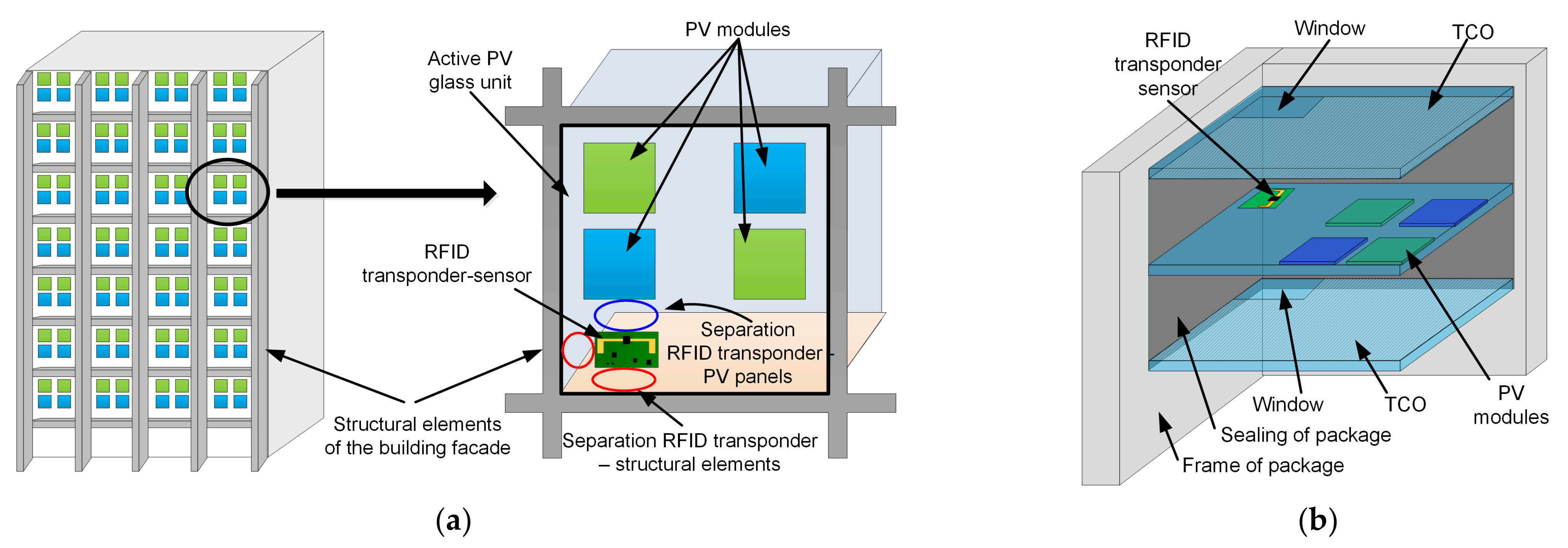
1.1. Object under Investigation

Glazing units are frequently used in modern multi-storey buildings to create amazing facades (Figure 1). When they are integrated with photovoltaic (PV) modules, active units are obtained. Generally, PV cells are located in the inter-pane spaces and, primarily, convert solar energy into electricity, although they can also serve as decorative elements, complementing the appearance of the building facade in accordance with an architectural vision. It is desirable, mainly for economic reasons and in order to ensure the high efficiency of a micro-photovoltaic power plant, that the active glazing units are equipped with a system for monitoring their operating parameters. With this comes design problems that go beyond the area of building construction and renewable energy systems and fall within the scope of sensor technology. A significant improvement, but one which presents a research challenge, may be achieved by the incorporation of RFID technology in the designed monitoring system. The monitoring system, based on semi-passive RFID transponders/sensors (RFID sensors), allows for data acquisition even if the PV modules are not active, as well as when they are disassembled or destroyed. In such passive modes, the power supply of the electronic circuit is conveyed by the electromagnetic field generated by the read/write device (RWD) [1]. This means that the transponders need to be well-designed, with special attention paid, firstly, to the energy balance and, secondly, to antenna performance. In addition, the technique of RFID sensor assembly in the active glazing unit needs to be carefully thought through. These factors determine the methodology required for effective diagnostics to be applied to the photovoltaic modules. Although the current–voltage characteristic is the most important parameter that could indicate PV cell condition, it is not necessary to monitor both quantities. The costs of implementing a current (power) transducer are too high, especially with respect to RFID systems, and entails interference in the main power wires. Instead, a comparative method can be used. All modules in one chain on the façade, under the same illumination and temperature, must provide the same voltage at the output terminals. Thus, a malfunctioning PV module can be identified, both by comparing the measured voltage between adjacent cells, or by relating it to the reference I-V curve. In this way, an RFID transponder-sensor need be equipped only with a voltage sensor; such a construction can be readily achieved given the current state of electronic technology.
The effectiveness of such a system depends primarily on the correct design of the transponder antenna. The subject of RFID antenna synthesis has been discussed frequently in the research literature; consideration of the design of an effective electronic tag is not new [2,3,4,5,6]. Unfortunately, there are no universal ‘off-the-shelf’ devices that could be used directly in non-standard utility applications. That is why many designs dedicated to specific applications (e.g., automotive [4] or pharmacy [5]), or that can work in a specific environment (e.g., near metals [2,3,6]), have been developed. In practical applications, in terms of engineering tasks, such designs are possible because the structure and operation of the specified object is precisely known, so the input parameters for numerical models of RFID antennas can be readily defined. In the case of active glazing units no comprehensive analyses of their parameters have been performed. Thus, the main purpose of the presented analysis is to prepare appropriate input data for design tools used in the synthesis of antenna systems in the UHF band.
From the construction side, with respect to antenna synthesis, the active glazing unit typically consists of two, three, or more glass panes or laminates. The inter-pane spaces are filled with thermally insulating gas, and the entire unit is properly sealed. Additionally, the surface of the outer panes/laminates is covered with an anti-reflective TCO (transparent conductive oxide) or heating layer. The panes are mounted in metal-structure facades, most often made of aluminium. In such an environmental arrangement, the implementation of effective communication with the master unit (or monitoring host, RWD) of the monitoring system, based on RFID technology, is mainly limited by the conditions of electromagnetic wave propagation between the antennas of devices [1,7]. For this reason, it is very important to carry out a thorough synthesis process of the antennas of an autonomous semi-passive RFID transponder/sensor, with the main emphases on maximizing the energy transfer to the RFID chip and shaping the radiation pattern.
The implementation of the UHF RFID system in the described application is associated with many problems, mainly related to the integration of the transponder antenna with the active glazing unit. The most important of these are:
  • proximity to the structural elements of the building facade (metal, glass, reinforced concrete, etc.) and the PV cells (Appendix A), which disturbs the shape of the radiation pattern and affects the impedance parameters of the antenna system;
  • presence of the conductive TCO or heating layer which is a barrier to the electromagnetic field;
  • the need to ensure easy integration of the RFID sensor and the specified object, without significant interference in the production of glazing units;
  • appropriate shaping of the radiation pattern in order to provide the possibility of reading and writing the RFID tag, both from inside and outside of the building; and,
  • impedance matching to the selected RFID chip in the broadest possible frequency range, at minimum in the bands 865–868 MHz and 902–928 MHz.
Bearing in mind the need to obtain the largest possible interrogation zone (IZ) [1,8], and thus the largest range of writing and reading from the internal memory of the RFID transponder, it is important to develop a design of the antenna with circular or elliptical polarization and an appropriately shaped radiation pattern (preferably omnidirectional). Moreover, according to the purpose of the designed application, the long-range RFID system of the UHF band, standardized in ISO/IEC 18000-63 [9], and adjusted to the electronic product code (EPC) [10], is the most suitable
choice. The RFID devices involved must comply with the European ETSI EN 302 208 standard [11], where the limitation on radiated power is set to 2 W ERP (effective radiated power) in the 865.6–867.6 MHz band. Within the American jurisdiction, compliance with the FCC Part 15.247 [12] is required; at 1 W of output power from the transmitter, with an antenna with a maximum gain of 6 dBi, the limitation is equal to 4 W EIRP (effective isotropic radiated power) in the 902–928 MHz band.
Due to the structure of the active glazing unit, the RFID antenna can only be placed on the surface of one of the glass panes/laminates. The most advantageous location appears to be the hermetically sealed inter-pane space. Consequently, the antenna system is secured against harsh environmental conditions, damage (e.g., mechanical damage during facade maintenance), and unauthorized access. Bearing in mind aesthetic requirements, one of the corners of the active glazing unit is an effective, though somewhat demanding, location (Figure 1a). The proximity of metal objects (e.g., building facade elements) causes a problem with the impedance matching of the antenna and the RFID chip, as well as causing significant disturbance of the radiation pattern. For this reason, it is necessary to ensure the spatial separation of the RFID transponder from the structural elements of the building façade, including PV cells. In order to eliminate the negative effects of the TCO or heating layers shielding the electromagnetic field, it may be necessary to make an opening (e.g., a window in the layer) to deliver radio waves to the antenna system (Figure 1b).

1.2. Concept of the Problem Unravelling

The RFID sensor hardware is based on the popular AMS SL900A chip (AMS AG, Premstätten, Austria), but the analysis can be applied to any RFID chips. As in a standard electronic transponder, the RF front-end is used to both exchange data as well as to receive power from the electromagnetic field generated by the read/write device. Additionally, the SL900A chip is equipped with extra output for providing external electronic circuits with excess energy. The extension supply block is connected, inside the semiconductor structure, to the antenna inputs of the integrated circuit. This characteristic must be taken into consideration when designing the antenna with the impedance matching circuit. In the majority of constructions described in the literature [13], or available on the commercial market, the matching circuit is made as a T-type component, with a parasitic inductive loop or discrete element, e.g., a coil attached to one of the antenna arms. However, the use of constructions with separated arms, tuned with planar or discrete inductances, causes problems in design. Among others, such a structure is susceptible to detuning (e.g., in the vicinity of metal objects), as well as being affected by even relatively small changes in the geometric dimensions of the radiator (e.g., during sample production), reflected in fluctuations of the impedance value, such that impedance matching in the RF front-end is possible in only a narrow frequency band (e.g., 865–868 MHz). On the other hand, the impedance matching loop short-circuits the input terminals of the RF unit for DC current, and blocks transponder activity [14]. However, it is worth paying attention to this construction, because it enables impedance matching of the antenna to the RFID chip over a wide frequency range (e.g., 860–960 MHz), despite its simple structure [13]. Additionally, this solution is more resistant to harsh environmental conditions, such as the presence of a metal frame, a glass substrate, or a layer of transparent conductive oxides [13]. In the case of the SL900A chip, it is then necessary to use the so-called DC block. This system is in the form of, for example, a capacitor with an appropriately selected capacitance (Appendix C), attached to one of the antenna arms. It transmits signals with the operating frequency f0, hence its use ensures correct operation of the energy harvesting block, despite connecting a compact antenna to the terminals of the SL900A chip.
Consideration of the use of RFID antennas, optimized for use on glass substrates, typically automotive glazing, can be found in the relevant literature [15,16,17]. These structures are usually dedicated to work in harsh environmental conditions (e.g., near metal) and are constructed as a modification of dipole antennas (with linear polarization). Other studies [18,19] have proposed designs with a different polarization, but their application in the context of the present research is not possible due to the spatial construction of their radiators. A typical problem is with the RFID chip position inside the structure of the proposed antenna circuits, which makes it impossible to feed signals to the measurement module. In [20,21], the transponder antennas have the quasi-omnidirectional radiation pattern but, in these examples, the inductive loop around the RFID chip is excessively complicated.
On the basis of analyses carried out in the field of the influence of components used in the active glazing units on the RF front-end (Section 2), three methods for the localization of the antenna system are proposed (Section 3): on the glass surface with a fragment of the TCO layer removed; directly on the glass pane covered with the TCO layer; and on the glass pane with the TCO layer, but with an additional passive reflector located directly under the radiator.

2. Materials and Methods

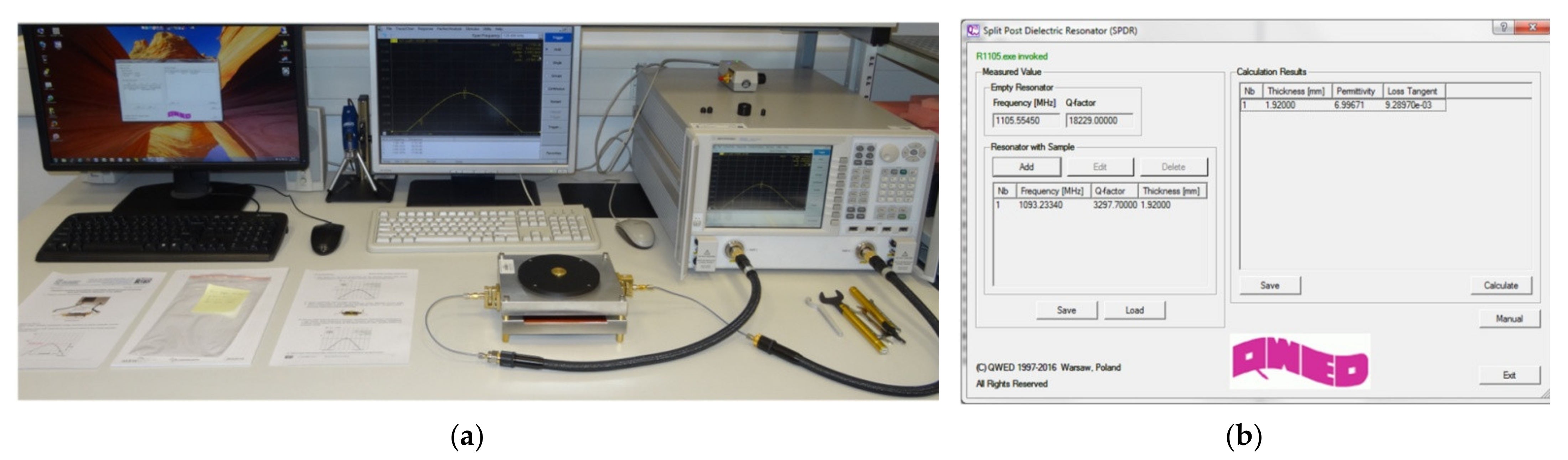
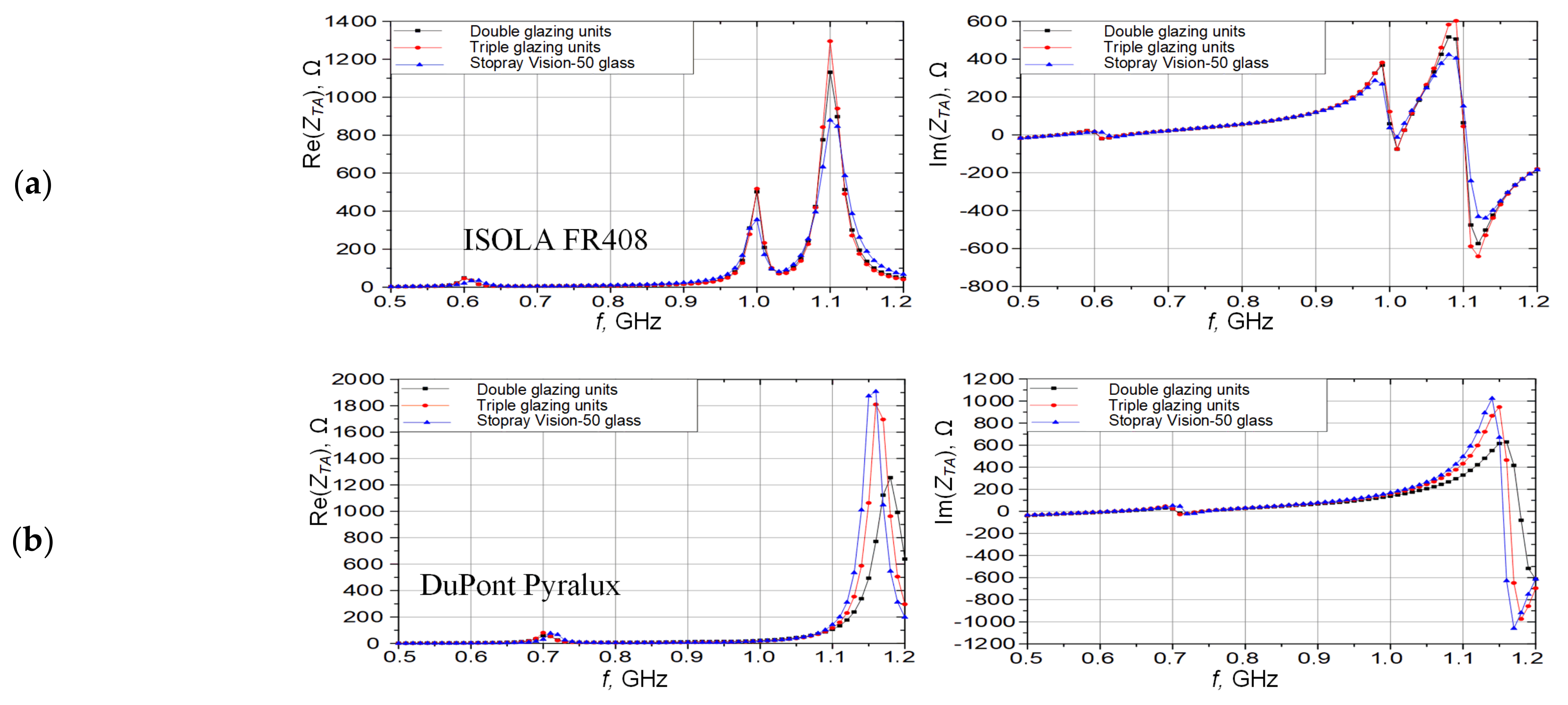
2.1. Characteristics of Materials

The precise characteristics of the material parameters of the structural components used in the construction of RFID transponders are key elements when designing effective antennas and matching circuits. Above all, it is necessary to characterize: (a) the substrates used in the RFID sensor, and (b) the panes/laminates, functional layers, and frames of the PV glazing sets [22]. The dielectric properties of these materials are described by the relative permittivity εr and the dielectric loss tgδ.
The parameter investigations were based on the frequently used materials: glass epoxy copper clad laminate ISOLA FR408 (ISOLA GmbH, Düren, Germany; laminate thickness of 0.510 mm, copper layer thickness of 18 µm) [23] and flexible laminate DuPont Pyralux LF9150R (DuPont, Wilmington, DE, USA; laminate thickness of 0.125 mm, copper layer thickness of 35 µm) [24]. The dielectric parameters of the RFID transponder substrates have previously been characterized in detail [23,24].
In the case of glazing units, the characteristics were based on representative glass samples with a size of 15 × 15 cm taken from products available on the commercial market. Due to the lack of precise information on the dielectric parameters [25], extensive research needed to be carried out in terms of the impact of the glass on the design of the RFID sensor antenna circuit (Table 1).
Low-iron glass (Table 1, Position 1, from an unknown manufacturer) is a high-gloss index glass that is made of silica with low iron oxide content (typically around 0.01%). Low-iron laminate is a combination of two of the same layers of glass separated by an SKC EVA sheet. The low iron content removes a greenish-blue tint and this type of glass is used where high transparency is required, e.g., as a covering glass in PV panels. The product is available as various brands of many manufacturers including: Guardian Industries (Bertrange Luxembourg), UltraWhite brand; Pilkington (Lathom, Lancashire, England), Optiwhite brand; PPG Industries (Pittsburgh, PA, USA), Starphire brand, and others. The PILKINGTON NSG TEC 250 is a glass with a transparent conductive layer of metal oxides with a resistance determined in [25]. This product is used in transparent heating elements, PV modules, etc.
In addition to the above-mentioned samples of glass and laminates, representative models of AGC glazing units (AGC, Tokyo, Japan) were prepared. All units were fabricated with dimensions of 20 × 30 cm as a single-chamber, double-glazed (Stopray Vision-50) unit, or two-chamber, triple-glazed (Stopray Vision-72) unit. In both cases, the outer layer was made of 6 mm float glass, one-side coated with TCO of undefined thickness and resistance (no data on the parameters were provided in the manufacturer’s technical documentation). The glass with such a coating provides good solar and thermal performance. These types of unit are especially suitable for non-residential buildings with air conditioning, because the applied layer of the Stopray Vision helps to maintain a pleasant temperature while minimizing energy costs.
The dielectric parameter determination was carried out in a specialized laboratory stand (Figure 2). Measurements were made at the frequency of 1.1 GHz (close to the selected UHF band of the RFID system) using a split-post dielectric resonator (SPDR by QWED Sp. z o.o., Warsaw, Poland)) and a vector network analyzer Keysight PNA-X N5242A (Keysight, Santa Rosa, CA, USA). In addition, a set of special cables was used, such as the flexible Keysight 85131F cable set and the Huber + Suhner Minibend cable assembly. The measuring algorithm included a stand calibration procedure, determination of the resonance frequency and of the quality factor of the dielectric stack arrangement for the test sample. The required parameters of the measured dielectric layer were determined using the dedicated QWED software based on a mathematical model of the SPDR [26].

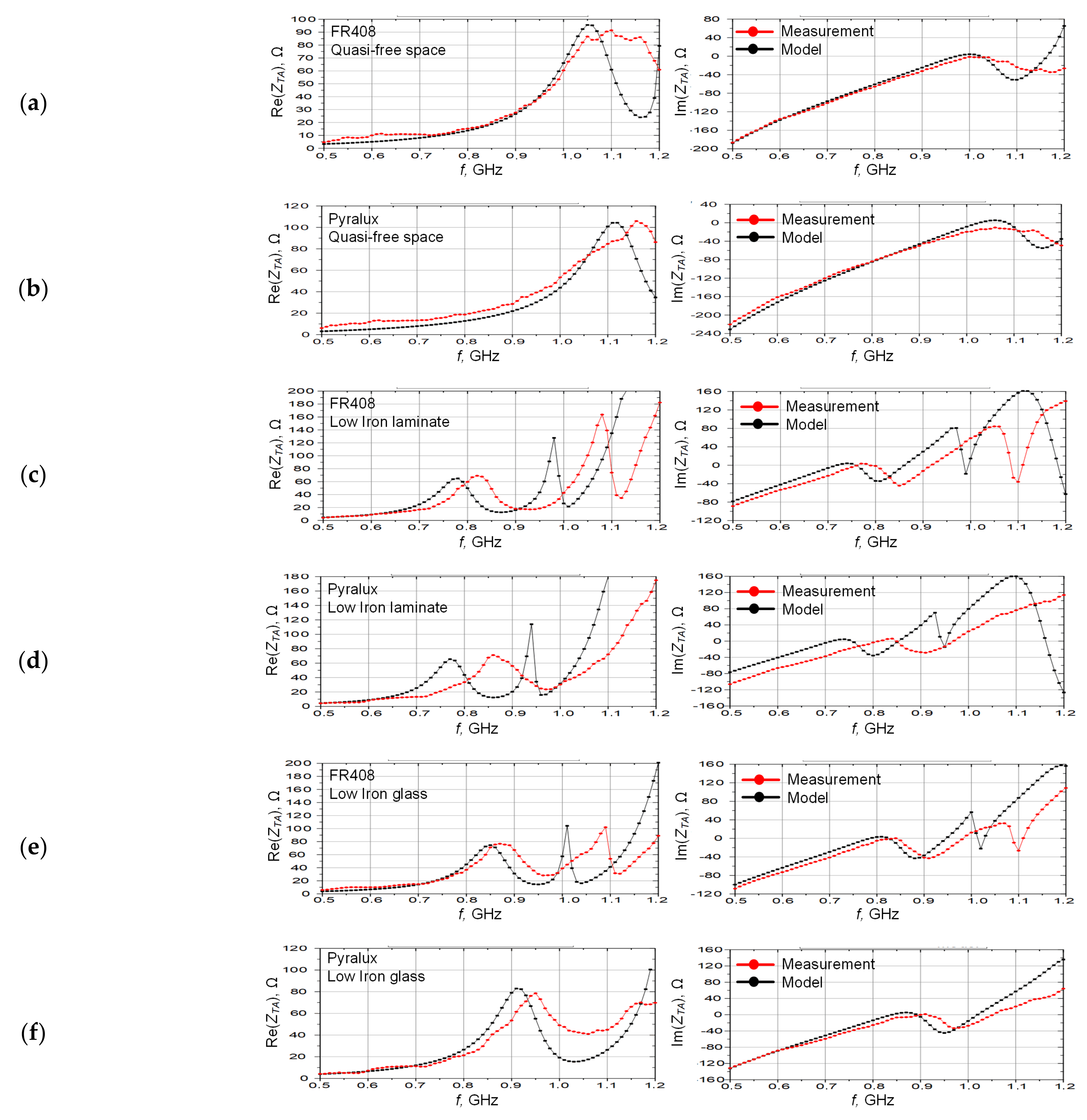
2.2. Pane Impact on RFID Antenna Performance

When designing the RFID transponder, it is necessary to know the influence of structural elements of the active glazing unit on the antenna efficiency. As an example, for confirming possible dependences, an antenna, including a modification of a half-wave dipole, with bent arms was selected (Figure 3) from the authors’ database of developed models. By its nature this construction is sensitive to the influence of environmental conditions. Impedance matching to the SL900A chip was achieved by connecting a discrete inductive element (SMD coil) to one of the arms. As a result, it was possible to tune the antenna without having to change its geometrical size. The samples were made on an ISOLA FR408 PCB (Figure 3a) with a DuPont Pyralux flexible substrate (Figure 3b,c). The possibilities of antenna localization on the surface of the common low-iron laminate (Figure 3a,b) and on low-iron glass were considered in the research. The correctness of the computational models was checked by comparing the calculated and measured ZTA impedance values (Figure 4). The specified arrangements were also compared to the model (Figure 3d) of the antenna located in the quasi-free space (plastic net under the sample, Figure 3c). The measurements were carried out on a special test stand equipped with differential probes and VNA [27], using 15 × 15 cm samples of low-iron glass and laminate.
Small discrepancies were noticeable between the measurements and the calculations at higher frequencies when the antennas located in the quasi-free space (for FR408: Figure 4a, Pyralux: Figure 4b) were considered. The value differences are irrelevant for RFID systems operating in the European UHF band and the samples and model are prepared correctly.
In the case of using the low-iron laminate, the impedance curves had the same shape but the measurement results for both the FR408 (Figure 4c) and Pyralux (Figure 4d) were shifted by approximately 50 MHz. It should be emphasised that the discrepancies are mainly visible as the shift of the curves in the frequency domain with almost the same shape of the curves, which would suggest incorrect determination of the dielectric parameters of the low-iron laminate.
In the case of low-iron glass (for FR408: Figure 4e, Pyralux: Figure 4f), the shift was noticeable especially at higher frequencies. It is worth noting, however, that close to the frequency range used by RFID systems in Europe, the differences in the impedance values for the numerical model and the samples can be considered negligibly small. This applies to the reactance, the values of which were similar for the model and the tested samples.
It is worth noting that also in this case the shift of the measurement results in relation to the reference data (from the numerical model) always occurred in the direction of higher frequencies, with almost the same shape of the curve. Although it is possible to design an efficient RF front-end, it should be kept in mind that any changes in the technology of glazing units will have a significant impact on the operation of the dipole antenna.
Therefore, two other antenna patterns with short-circuited arms (Figure 5) were taken into consideration in the investigations. Such a construction is less susceptible to the influence of the dielectric properties of surrounding materials. Since the SL900A was used, the DC component was blocked using the SMD capacitor built into the radiator. The soldering pads, as well as the gap in conductive paths, were included in the numerical calculations. The radiator also requires to be surrounded by a ground layer to further reduce the impact of environmental conditions.
The examined samples were modelled and manufactured on the FR408 laminate. The comparison of measurements obtained for the samples on the low-iron laminate with the model calculations of the antennas #A1 and #A2 is shown in Figure 6a,b. Although the curves in the graphs have a similar shape, the reference and measured data were significantly shifted in relation to each other in the frequency domain (by approx. 80 MHz and 100 MHz, respectively). Such discrepancies exclude the possibility of correct and effective operation of the so designed antenna in the RFID system. Replacing the low-iron laminate by low-iron glass (Figure 6c) lead to a similar discrepancy.
The values of the power transfer coefficient from the antenna to the SL900A chip were determined (Figure 7) based on the impedance measurements (Appendix B). This parameter, or the conjugate match factor (CMF), as it is referred to in some apparatus manuals, determines the quality of the impedance matching between the IC input and the connected antenna. If the CMF is equal to 1, then the RF front-end is perfectly matched. However, in the investigation case under consideration, the measured curves were a similar shape as for the calculated data, but they were shifted by nearly 100 MHz in the frequency domain. At the central frequency of the European RID UHF band (866 MHz), the value of the power transmission coefficient was less than 0.1 for the measured samples. This implies a lack of impedance matching and that this construction cannot work properly in an RFID system. Nevertheless, similar results were obtained regardless of the use of low-iron glass or laminate. On this basis, it can be assumed that a systematic error was the source of the discrepancies or that there were special properties of the low-iron glass (e.g., the presence of an additional conductive or dielectric layer), as the glass came from an unknown manufacturer and its characteristics were not exactly known.
In order to know the reason for the curve shift, the influence of the unknown characteristics of the low-iron glass (e.g., the effect of an additional conductive or dielectric layer) was checked in the first step. Impedance measurements were repeated twice for design #A2, separately for each side of the low-iron glass. Almost identical results were obtained in both cases (Figure 8a). A further test, using NoName glass, was also undertaken in order to confirm the validity of the observed dependencies. The observed curve shift was consistent with the behaviour of previous experiments for low-iron glass (Figure 8b).
It was concluded, on the basis of the performed investigations, that the problem with the curves’ convergence lies in the validity of the antenna model. First of all, attention was paid to the correctness of modelling the arrangement of two dielectric materials in the stacks under consideration: glass and microwave laminate. Since the dielectric constant εr is the key parameter that influences the ZTA impedance, it is necessary to pay attention to the accuracy of determining its total value for the stack consisting of two layers—a detailed description of the problem can be found in publication [28] that is cited in most recent studies. It is unfortunate, but generally a consideration of this problem is omitted from software manuals dealing with the numerical calculations [29].
The resultant value of the dielectric constant of two or more materials is given by the formula:
ε e q = n = 1 N t n ε n 1 n = 1 N t n
where, εeq is the total value of the stack, εn is the value of the n-th dielectric layer, tn is the thickness of the n-th layer.
Additionally, a thin layer of air (0.4 mm) between the FR408 laminate and the glass surface was included in the model. Once the precisely described connection of dielectric layers was included in the calculations, a convergence of results was achieved (Figure 9).
Although there are noticeable curve shifts for the new designs, they can be considered negligible small. It should be noted that when designing the antenna structures, ideal models (infinite plate) of the substrate and glass were used. Since real materials are anisotropic, their surfaces are not perfect, and the measurement of the dielectric constant may be affected by uncertainties.

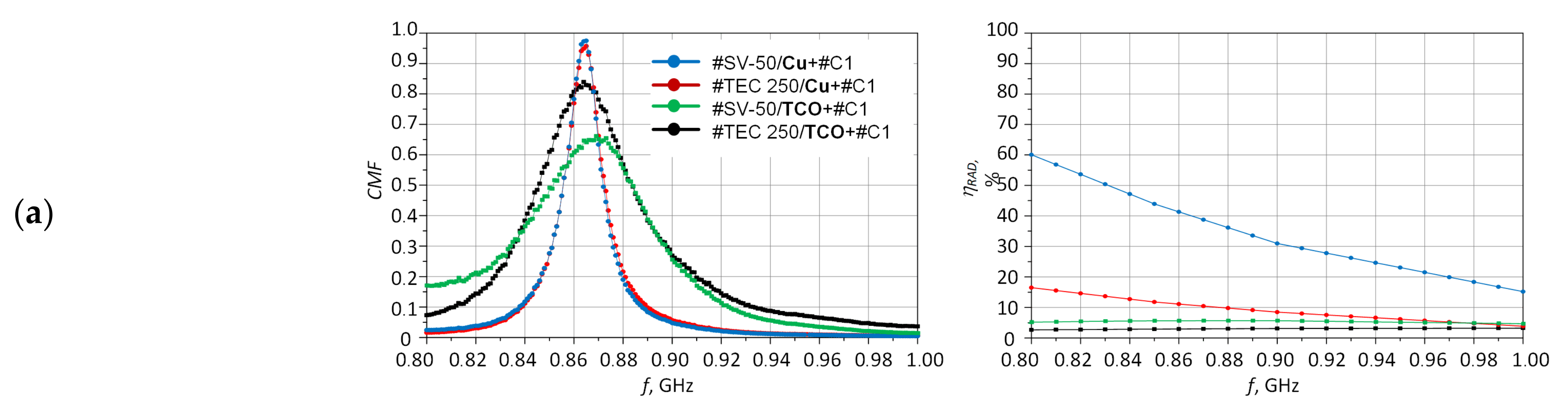
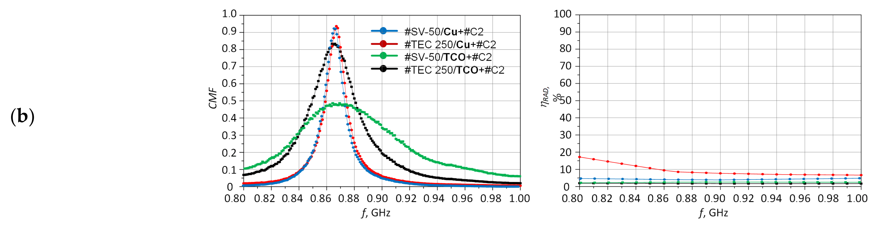
2.3. TCO Impact on RFID Antenna Efficiency

Since the outer panes of a typical glazing unit are covered with the TCO or heating layer, the possibility of locating the RFID antenna directly on such a glass surface would be very advantageous. Therefore, it is important to determine the impact of the extra thin layer on the antenna performance. The analyses were carried out as before for the modified half-wave dipole (Figure 3) with bent arms. The design was re-evaluated in order to take into account the material parameters of the pane made of AGC Stopray Vision-50 glass (Table 1). The samples of antennas were made on the FR408 PCB and Pyralux flexible substrate.
Determination of the dielectric constant for glass coated with a TCO is a big challenge, and is often subject to significant uncertainties. It is impossible to create the measurement sample with only the TCO because the properties of the thin coating and the bulk material are different. Furthermore, the calculations on the basis of formula (1) are substantially inaccurate, because of significant variations in the proportions between the thicknesses of the layers. However, the TCO influence can be checked by analyzing the convergence of measurements and calculations (Figure 10), and the proper value of εeq can be found. It should be noted, however, that full correspondence between the calculated data and the measurement results was not achieved in any of the cases considered.
The influence of the full glazing unit structure on the obtained calculation results was also checked for an elaborated model. The antenna samples were placed on a single pane made of Stopray Vision-50 glass as well as on full units of double and triple glazing. The obtained results were convergent (Figure 11), and slight differences in values occurred only in the areas of resonance.
In sum, designing the dipole-shaped RFID antenna, such that it is placed directly on the glass covered with the thin conductive layer, is possible, but it is a difficult task. Due to the negative effect of the functional layer, antennas of this type need to be very carefully modelled and precisely adjusted to the known dielectric parameters of the surrounding materials. Moreover, model simplification, involving considering only one pane of the glazing unit, is justified, and does not cause discrepancies.

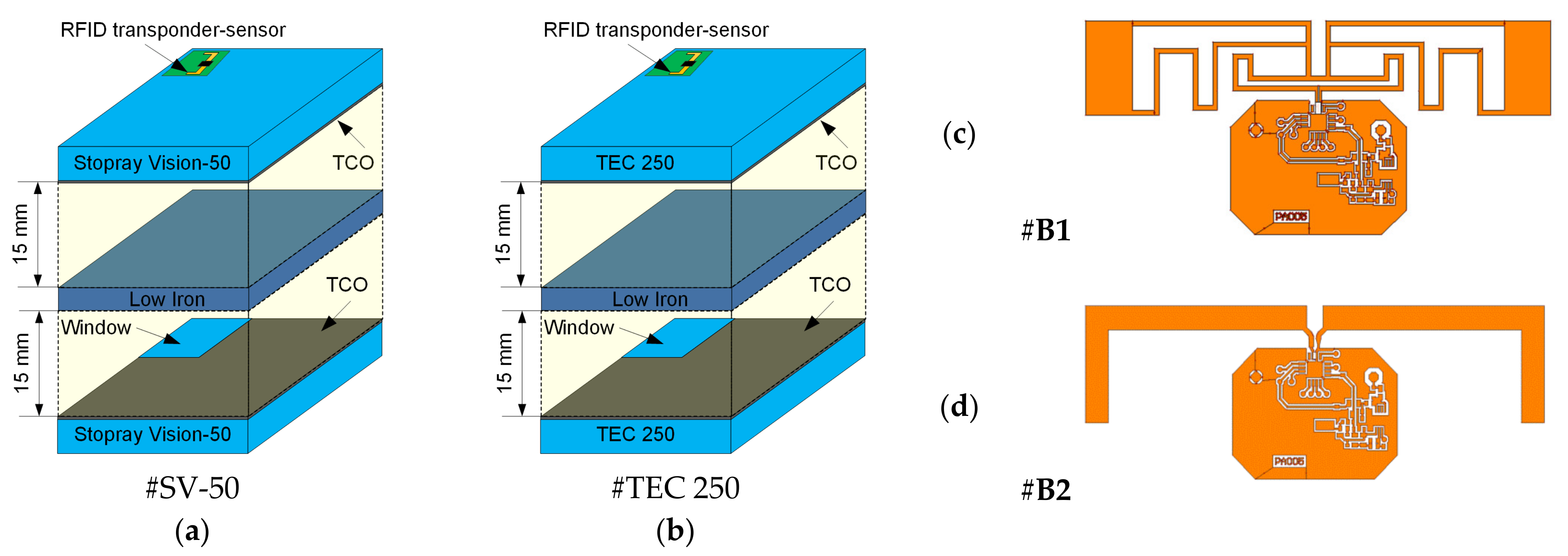
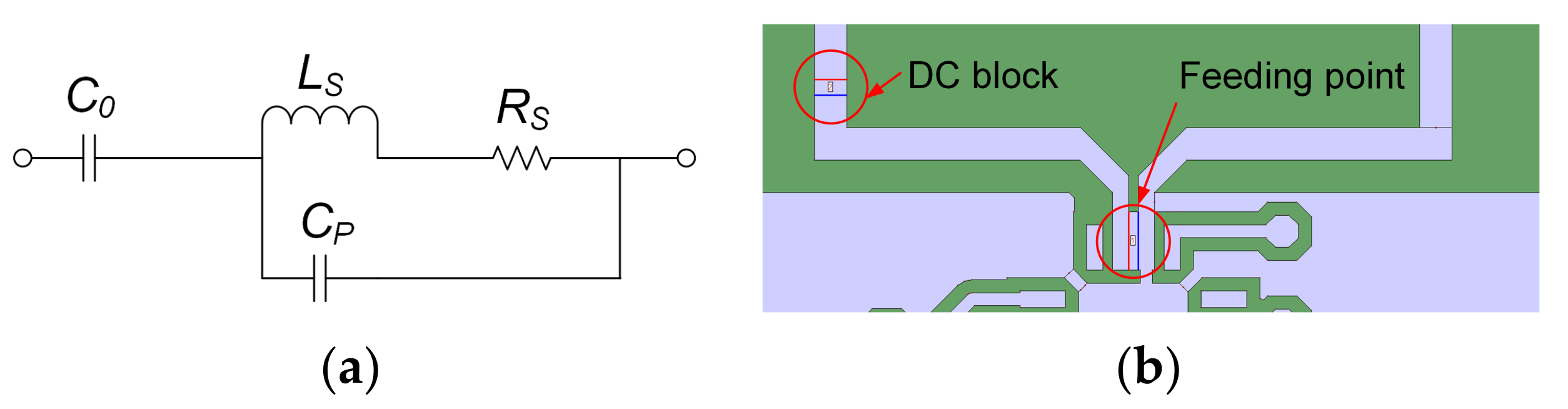
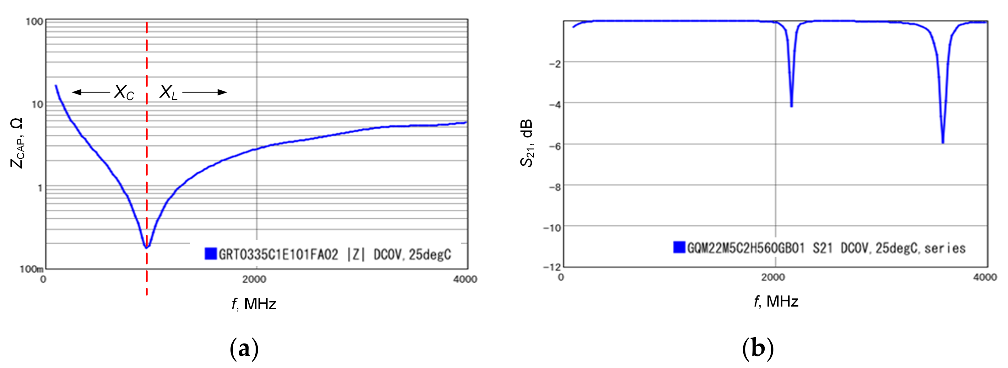
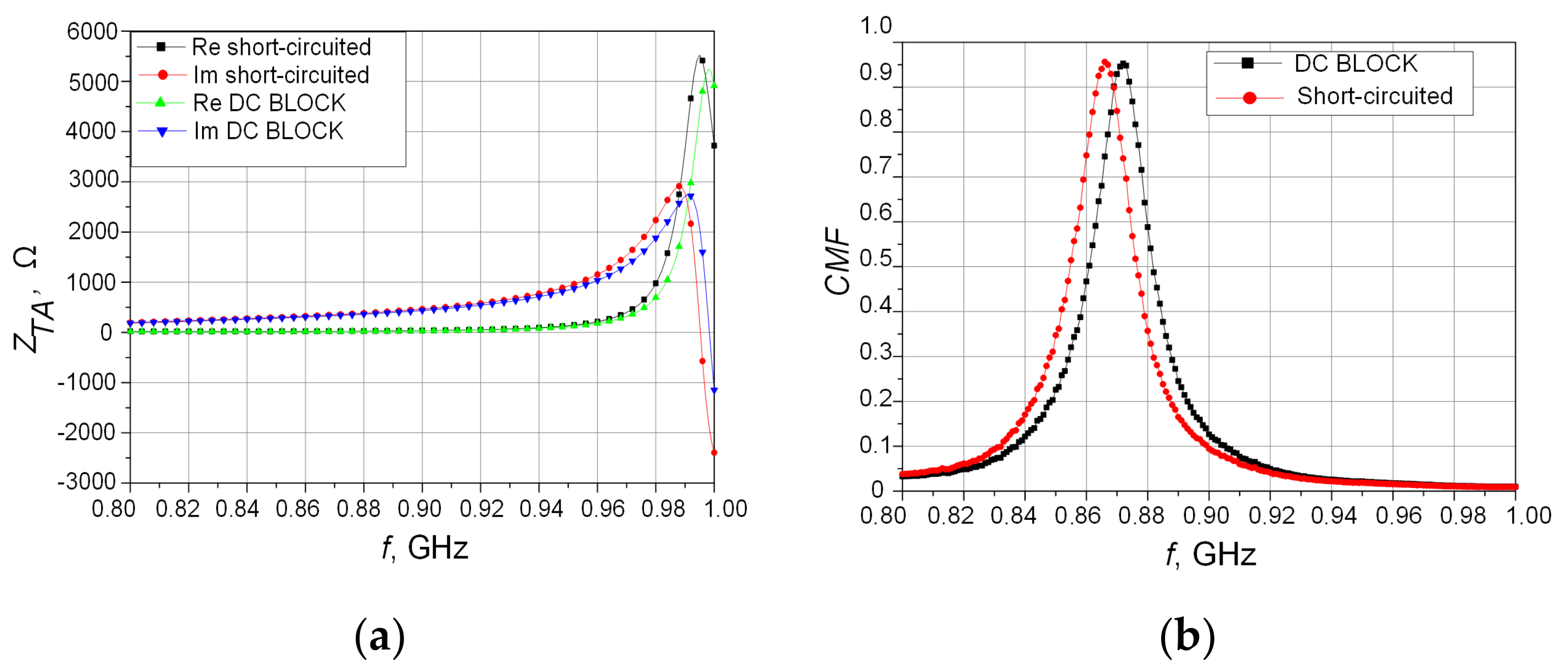
2.4. Immunity to the Influence of Application Environment

In the next step of the synthesis, an RFID antenna was designed with the reflector placed directly under the radiator. The knowledge gained from the investigations described in Section 2.1, Section 2.2, Section 2.3, was implemented in the new numerical model. The influence of the surrounding materials and the properties of the glazing unit (the glass thickness, its relative dielectric permittivity, the distance between panes and others) were predicted, and addressed by using a passive reflector in the form of a copper layer on the bottom side of the antenna substrate. The proposed construction was based on the prior developed design [14], with a view to operating in difficult environmental conditions, including in the vicinity of conductive materials (Figure 12). It is a two-layer structure designed for use with the ISOLA IS-680-300 microwave laminate (Table 1). The radiator, in the form of a monopole, as well as the paths of the electronic circuit, are located on the top side. All conductive paths are surrounded by the ground layer. The new antenna design also included additional passive components (ferrite beads) that separated the antenna circuit from electrical disturbances generated by the PV module and passed by sensors.
The obtained measurements for the samples and the calculated data of the reference model were convergent. The impedance resonances occurred at the same frequency points, and the shape of the graphs was almost identical (Figure 13a). There were slight discrepancies in the value domain, but only in the resonance area. The influence of the glazing unit components are presented in Figure 13b. A pane made of NoName glass (two cases were considered: with and without the additional reflector), and a pane made of NSG TEC 250 (Table 1) glass (each side was tested separately), were used in the experiments. Despite placing the antenna on the surface of materials with different dielectric parameters, the measured antenna resistance and reactance were similar to the values obtained in the case of quasi-free space (the differences in values occurred only near the resonances: 750 MHz, 860 MHz, and 980 MHz). The greatest discrepancies were noticeable for the NoName pane with the additional reflector. It can be concluded that the tested design of the RFID antenna was resistant to the influence of environmental conditions.
However, it should be noted that the proposed design is a monopole construction, so it may be sensitive to even slight changes in geometric dimensions (e.g., inaccurate sample preparation). For example, Figure 13c shows the measurement and calculation result discrepancy after modifying the layout of the electronic circuit by adding contact pads and making small changes to the ground layer.

3. Results and Discussion

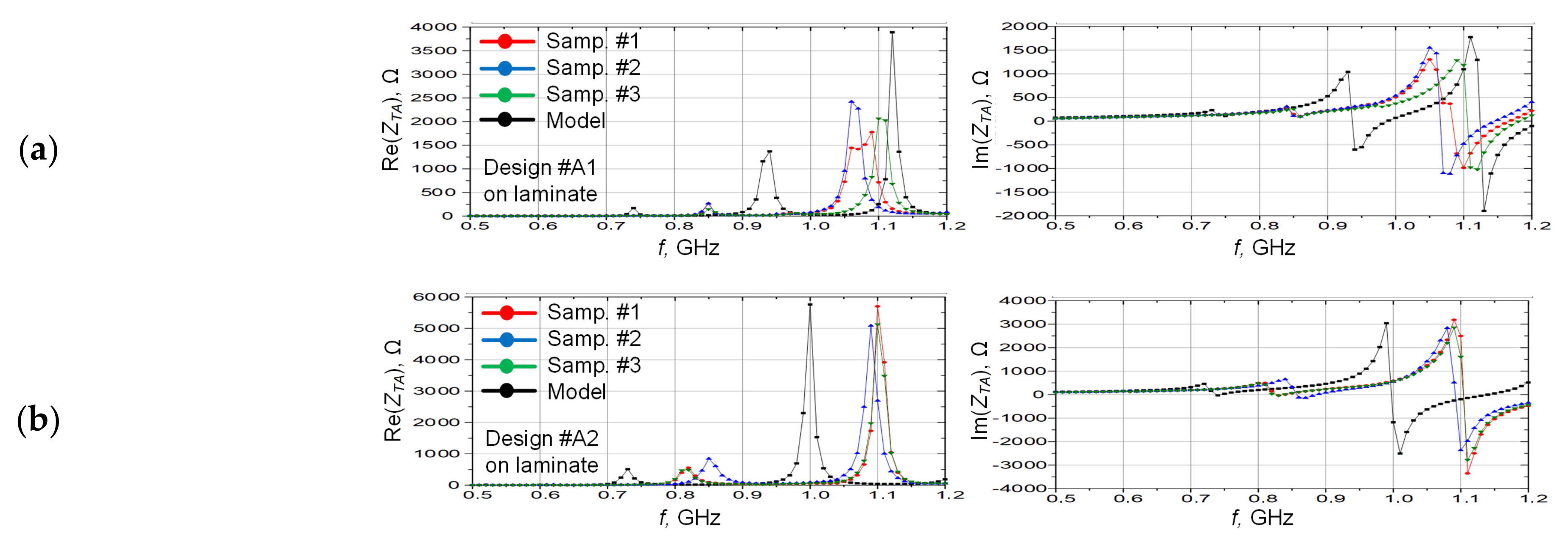
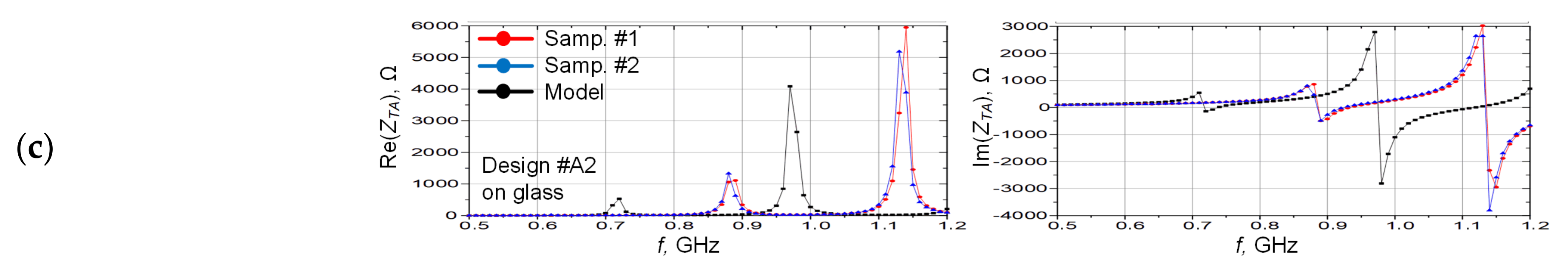
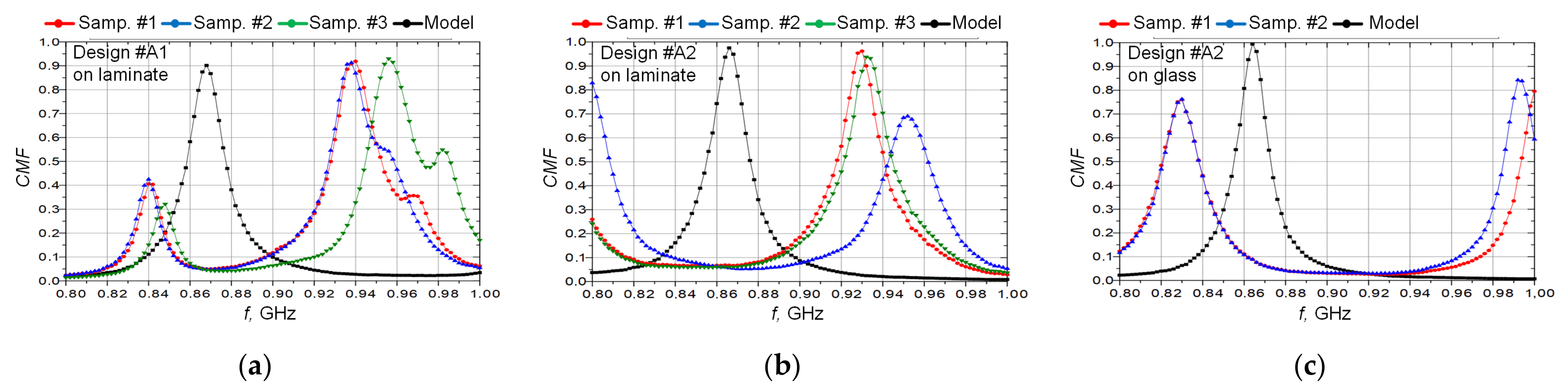
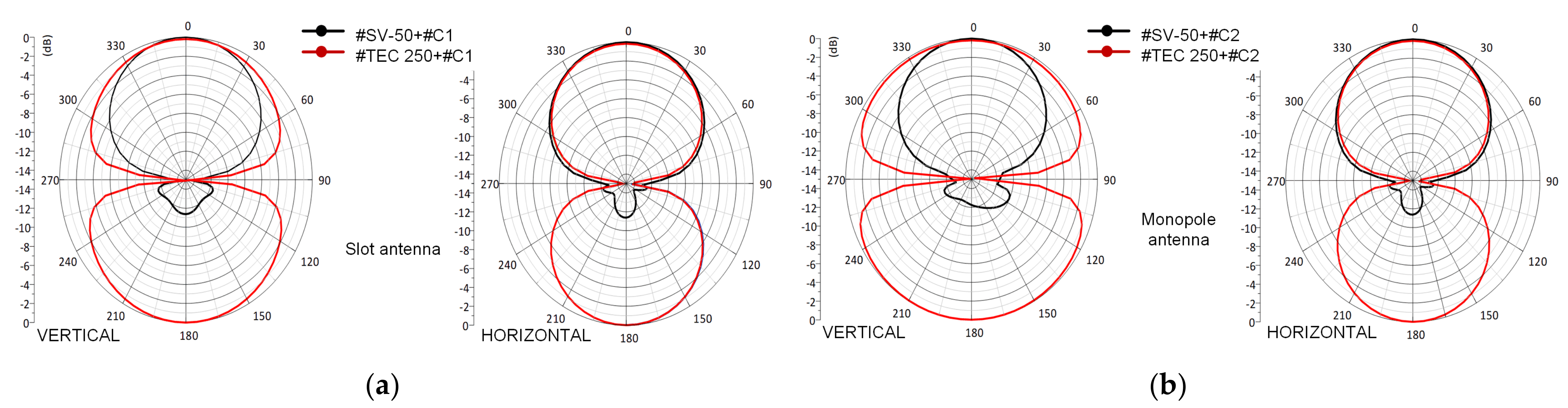
3.1. Bidirectional Antennas

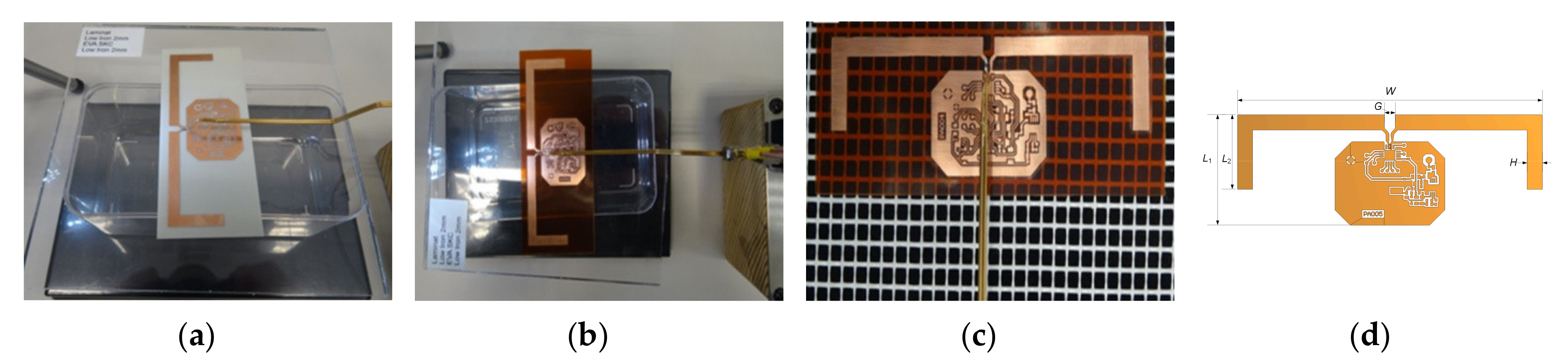
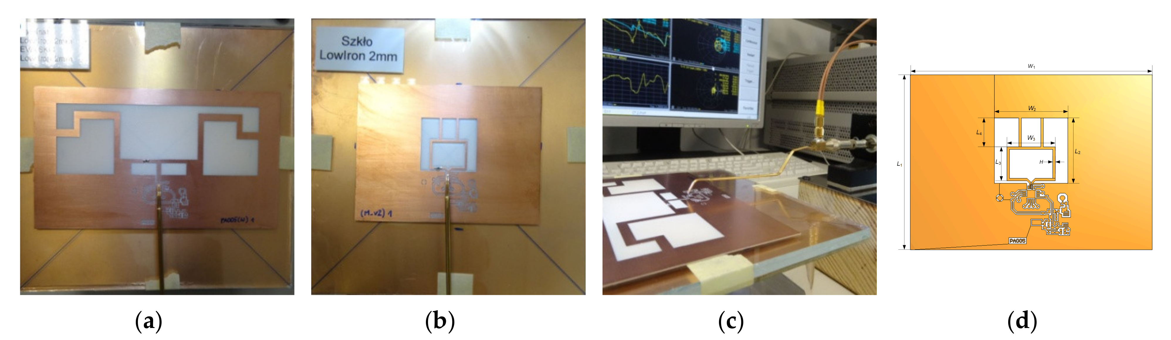
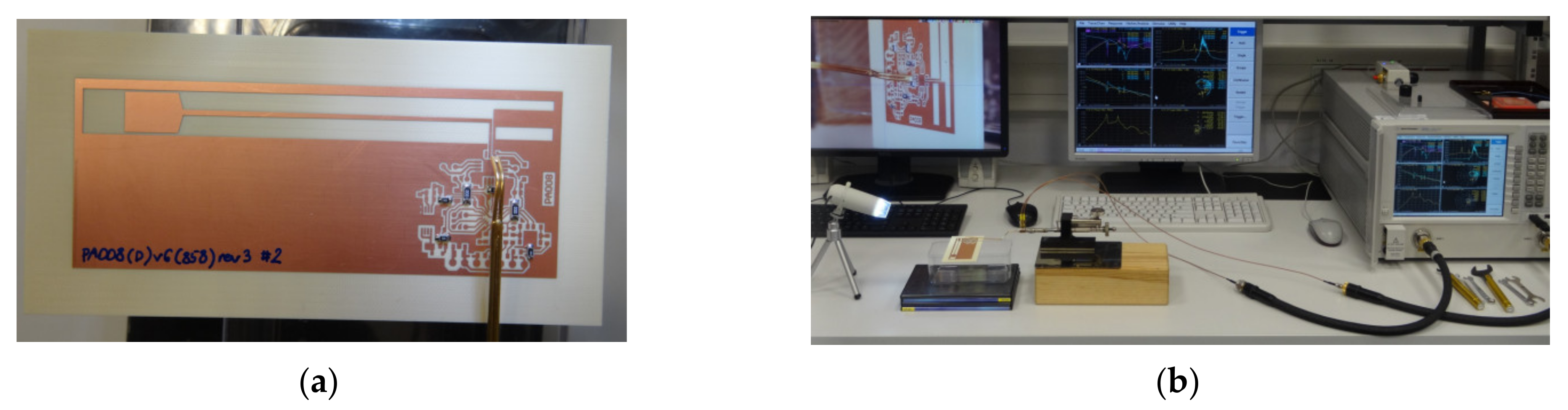
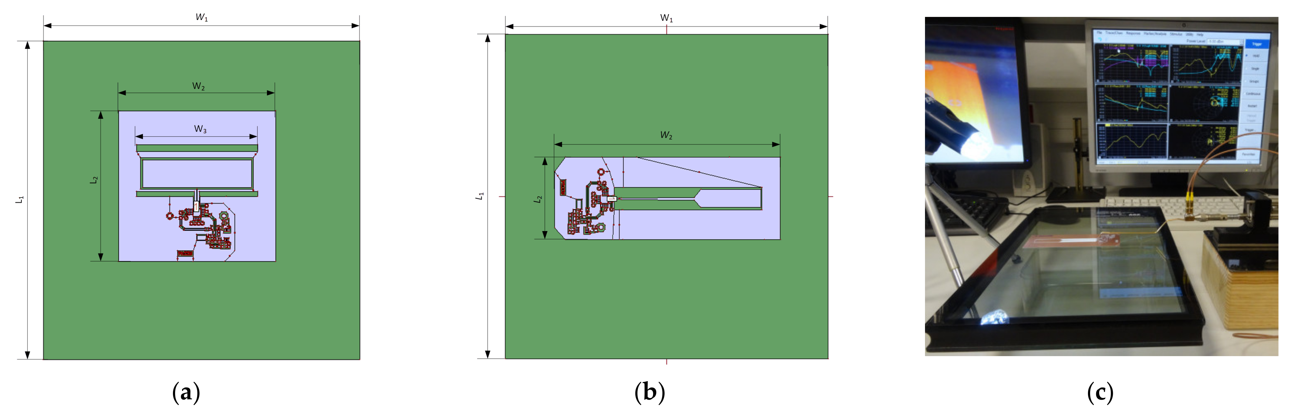
3.1.1. Antenna Design

The possibility of establishing radio communication from both sides of the active glazing unit (from inside and outside of the building) was one of the first concepts considered for the investigations into the synthesis of RFID antennas. With respect to the principles of RFID system operation, the TCO, or heating thin layer, has to be treated as the reflector or attenuator of electromagnetic waves. If such a layer is applied on the glass pane, in most cases it blocks the possibility of connecting the RFID sensor with the RWD. In order to solve the problem, it was proposed to remove (e.g., by laser ablation or mechanical grinding) the functional layer from a fragment of surface to create a window for passing electromagnetic signals. The geometric dimensions of the opening were assumed to be so large that the impact of the thin layer on the impedance parameters and propagation properties of the antenna system was considered as negligible in the research undertaken. The hypothetical location of the RFID sensor in relation to the structural frame of the glazing unit was also considered. According to functionality and the aesthetic requirements of the application, the best place for fixing the device was the corner but with sufficient distance from any metal elements (Section 3.2). Finally, the full triple-glazed unit, with the opening in the thin layer (Figure 14a,b), was implemented in the numerical model. The thin separation between the glass and antenna substrate was included in the calculation. It was assumed that the central pane was made of 1.92 mm thick low-iron glass, and that the inner and outer panes were made of Stopray Vision-50 or NSG TEC 250 glass (Table 1).
The investigations were performed for two antenna patterns designed for fabricating on the FR408 substrate (Figure 14c,d). The first design (Figure 14c) was elaborated as the meandered dipole with an impedance match circuit in the form of a loop. Since the chip’s input is short-circuited by the matching loop, the DC block had to be used, and pads for its connection had to be added in the numerical model. The second construction was a dipole with bent arms (Figure 14d). In this case, the impedance matching was achieved by use of an SMD coil attached to one of the antenna arms.
The calculations were carried out for four arrangements of the RFID antenna and the glazing unit: #SV-50+#B1, #SV-50+#B2, #TEC 250+#B1, and #TEC 250+#B2. As shown in Figure 15, the antenna #B2 showed a better impedance matching. It was also characterized by better propagation properties—the determined radiation efficiency had values several percent higher across the entire tested frequency band than for the design #B1.
From the radiation patterns shown in Figure 15c,d, it can be concluded that communication can be established on the both sides of the active glazing unit. Thus, the discussed concept of removing a fragment of the TCO layer is feasible. However, it should be remembered that mechanical treatment of the glass pane affects its insulating properties. Although the disproportions in the radiation level were noticeable between the values determined for the four considered arrangements, they did not cause a significant limitation of the read/write range.

3.1.2. Impact of Size of Opening in Thin Layer

As assumed in Section 3.1.1, the RFID antennas can only operate properly if a sufficiently large opening is created in the thin functional layers. Therefore, the influence of the functional layers’ proximity on the impedance parameters and propagation properties of the antennas #B1 and #B2 was examined in detail. The dielectric parameters of microwave FR408 laminate and a glass made of NSG TEC 250 or Stopray Vision-50, as well as the 500 nm thick TCO layer (green in Figure 16), were taken into consideration in the numerical model (Figure 16). A separation of 100 mm was assumed as the initial value of the distance between the antenna and the unit frame (Figure 16a). In the next steps of the calculations, the distance between the antenna and the TCO layer was increased equally on each side of the radiator (Figure 16b).
The antenna #B1 was less susceptible to the influence of the functional layer. The maximal value of the CMF was noticeably smaller for a separation below 2 cm, and shifted in the frequency domain. The type of used glass had little effect as shown in Figure 17—it can be seen, in particular, in the arrangement with the antenna #B2. As a result, the calculations performed confirmed the validity of the assumptions made in Section 3.1.1.
Thus, by introducing a properly selected spatial separation between the antenna radiator and the TCO layer (or the heating coatings as well as any other thin layers that are used in PV cells), the influence of this layer on impedance and propagation parameters could be effectively eliminated.

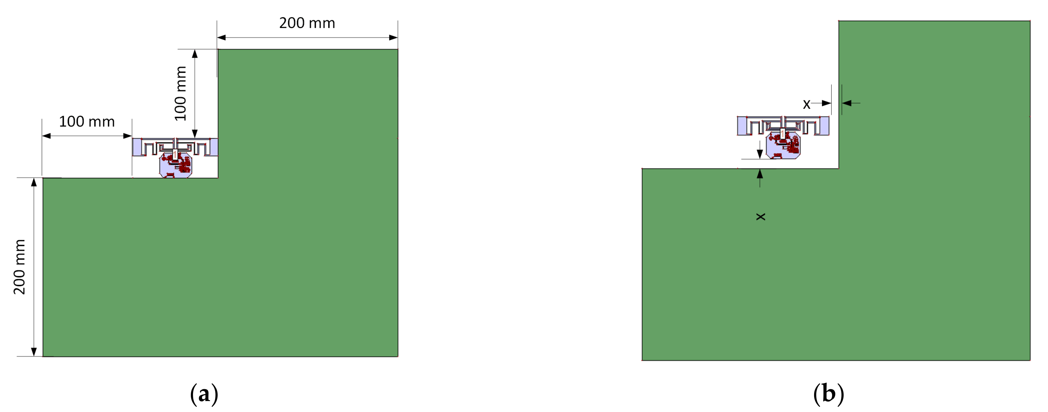
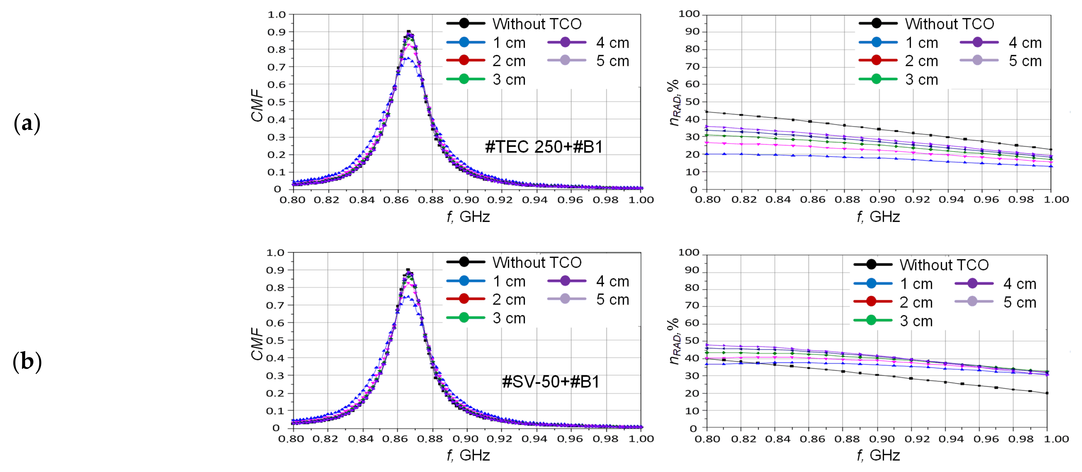
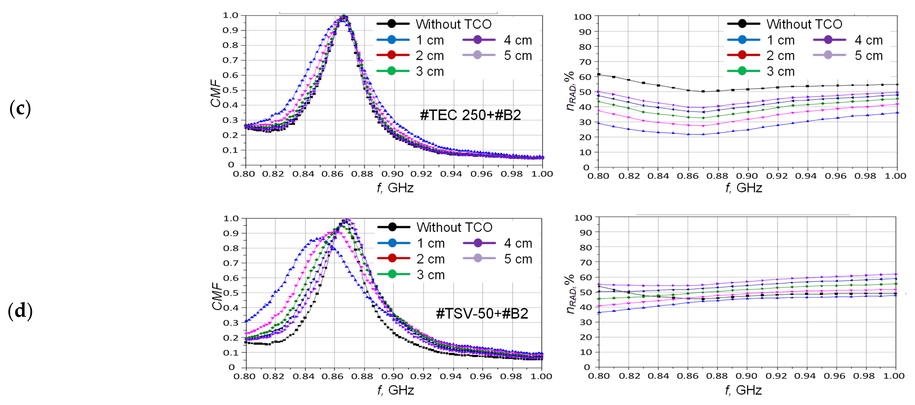
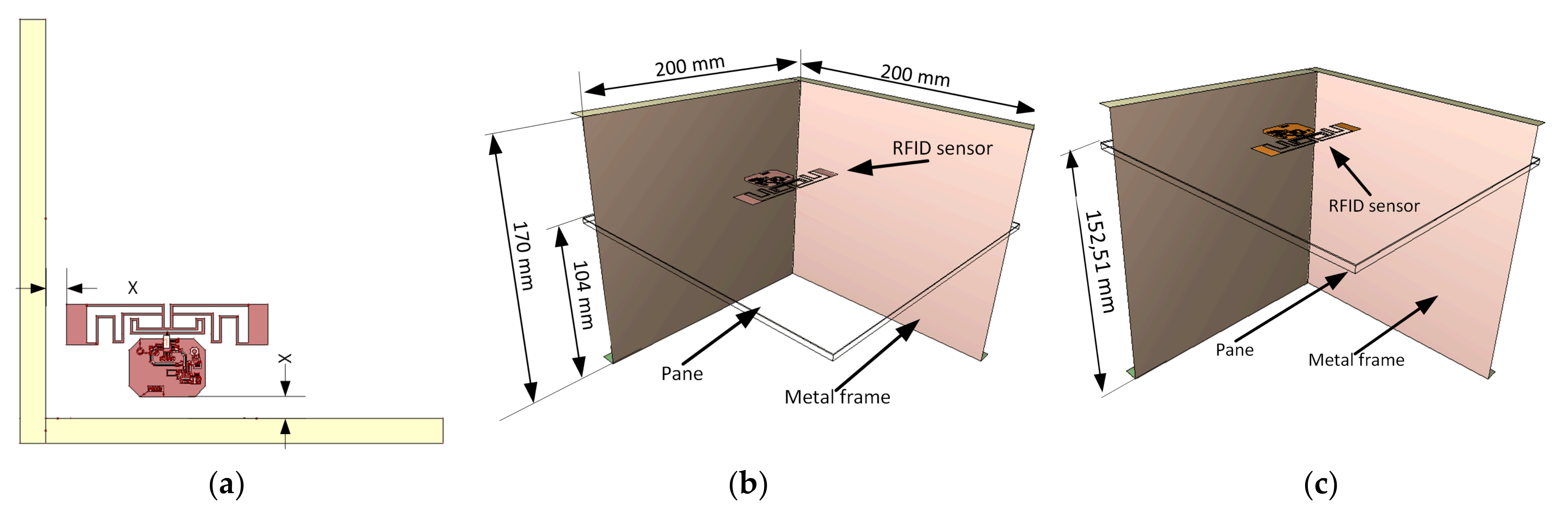
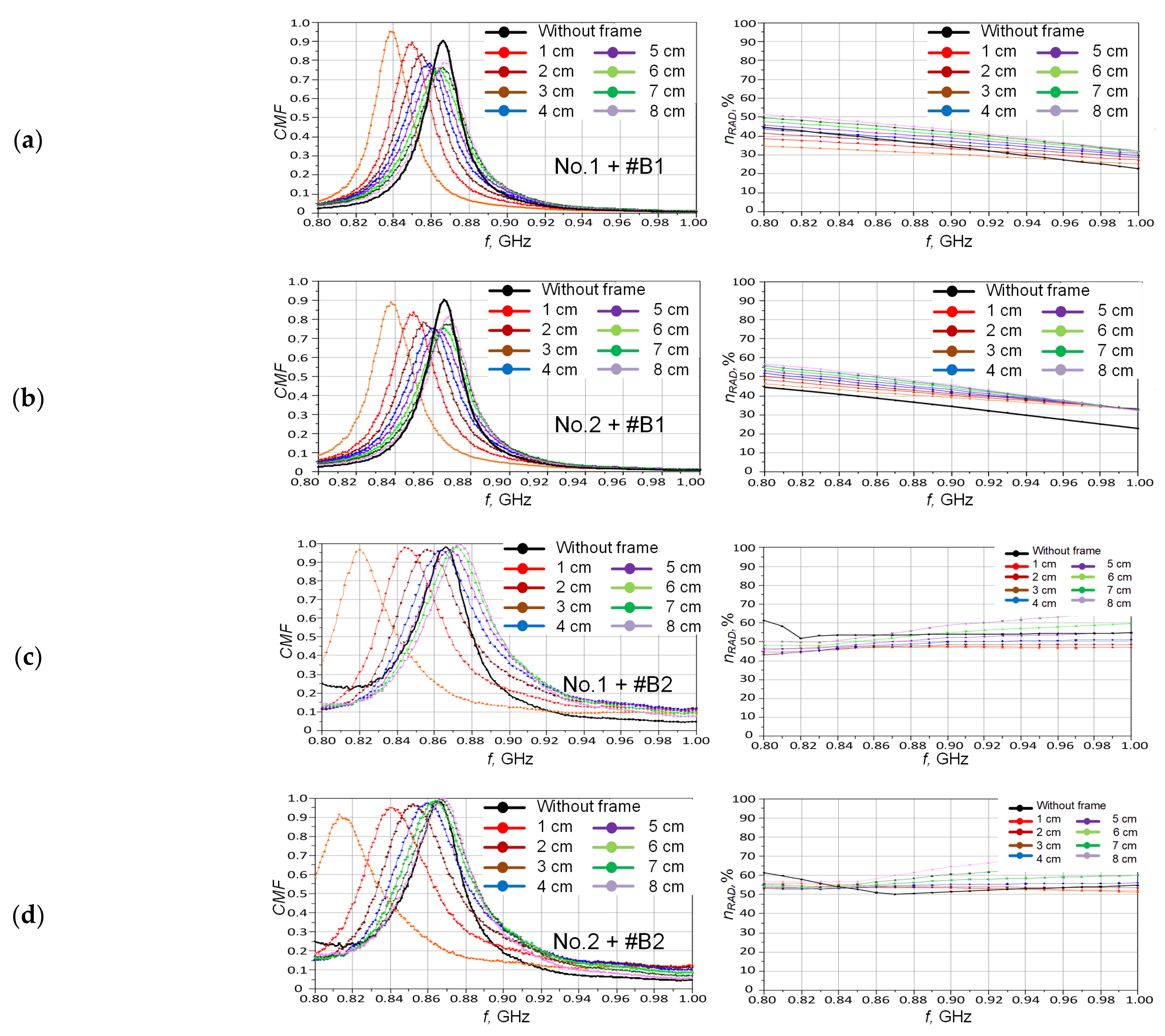
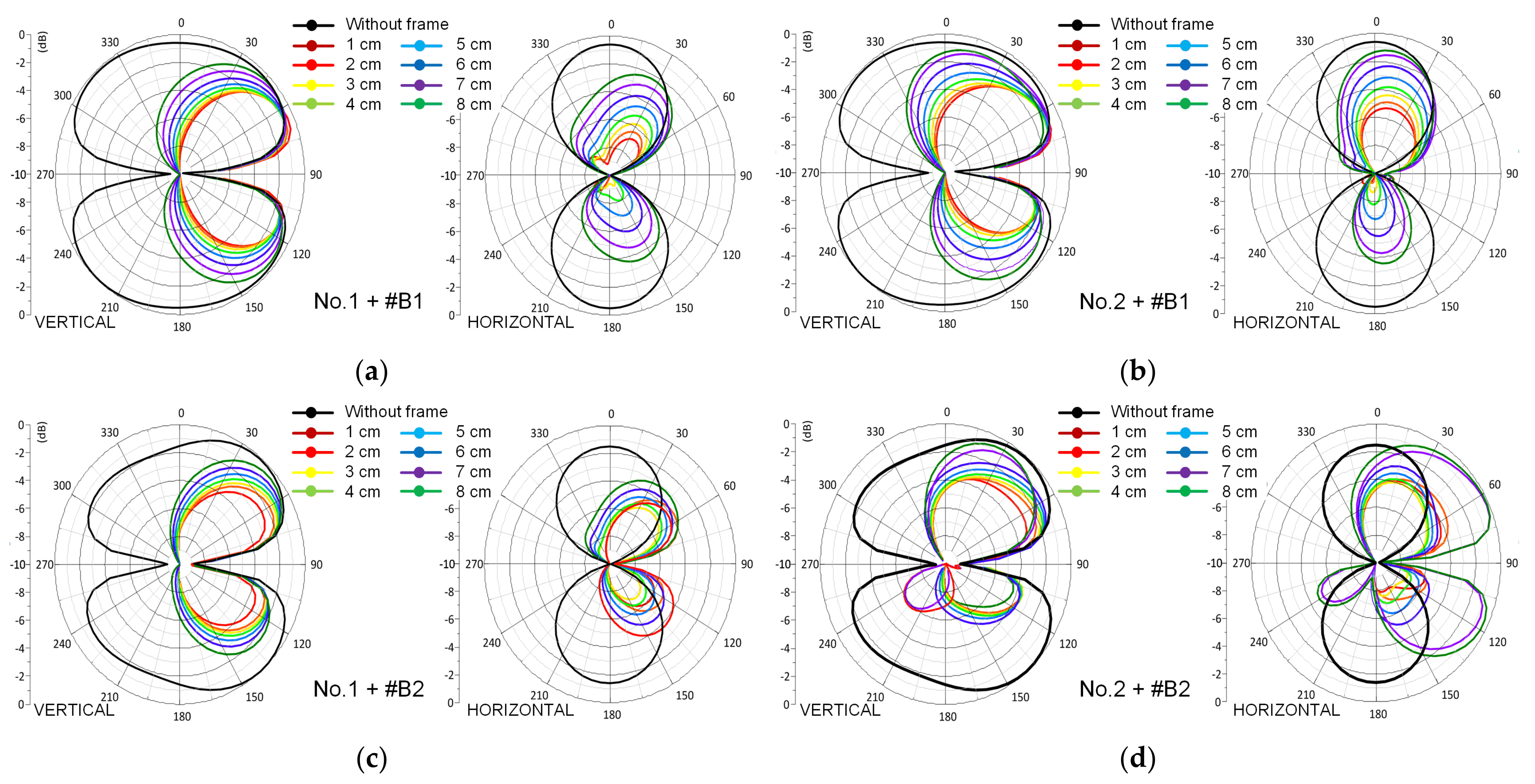
3.1.3. Impact of Unit Frame Proximity

The glazing unit metal frame impact on the RFID antenna parameters was also examined. Two aspects of this issue were considered in the numerical model. Firstly, eight cases of separation distance were considered: from 10 to 80 mm (Figure 18a). Secondly, two cases of RFID sensor location were investigated (Figure 18b,c). It was assumed that the tag is placed on the glazing unit surface that is closest to the inside of the building (No.1) and on the surface of the outer pane (No.2). The difference between cases No.1 and No.2 consists in the pane installation depth in the structural frame—the inner pane is mounted in the centre of the glazing unit frame, but the outer pane is 18 mm from the edge of the unit. The simulations were carried out for the antennas #B1 and #B2, fabricated on FR408 and placed on the NSG TEC 250 glass.
The proximity of the metal frame did not significantly affect the impedance parameters of the antenna #B1 (Figure 19a,b). There was a noticeable reduction in the maximum CMF value, but the frequency at which it occured changed only at small distances from the frame (up to 5 cm). A significant distortion of the radiation pattern shape was clearly visible, especially in relation to its horizontal plane (Figure 20a,b). However, as spatial separation between the radiator and the unit frame increased, the shape of the directional diagrams was more and more similar to the results for the numerical model, in which the frame was not included.
In the case of the antenna #B2, the proximity of the metal frame primarily caused shifts in the frequency domain, but the CMF maximum value was not affected (Figure 19c,d). As before, the distortion of the radiation pattern was significant (Figure 20c,d). In contrast to the case of the antenna #B1, as the separation from the frame increased, the shape of the directional diagrams increasingly differed from the results obtained for the reference model (without the frame). This problem affected both the horizontal and vertical diagrams. It is concluded that the antenna without the matching loop, despite good impedance and propagation parameters, is very sensitive to environmental conditions and, consequently, that design and maintenance problems may occur when implementing the antenna in the desired RFID system.
With respect to the need to establish radio communication from both sides of the active glazing unit (from inside and outside of the building), the two models of antenna can be compared. The meandered dipole, with the loop impedance match circuit and DC block, is a better choice than the dipole with bent arms and SMD coil as a matching element. Based on the simulation results, it can be clearly stated that the omission of the TCO layer and the metal frame of the glazing unit in numerical models does not significantly affect the calculation accuracy, provided that the spatial separation is included. The suggested minimum distances are 10 cm from the frame and 5 cm from the TCO layer.

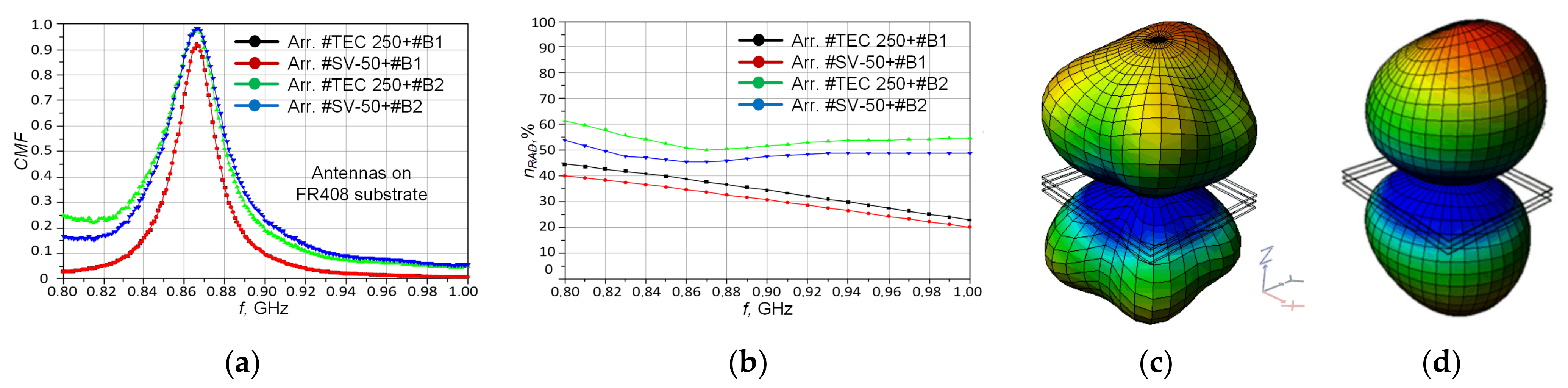
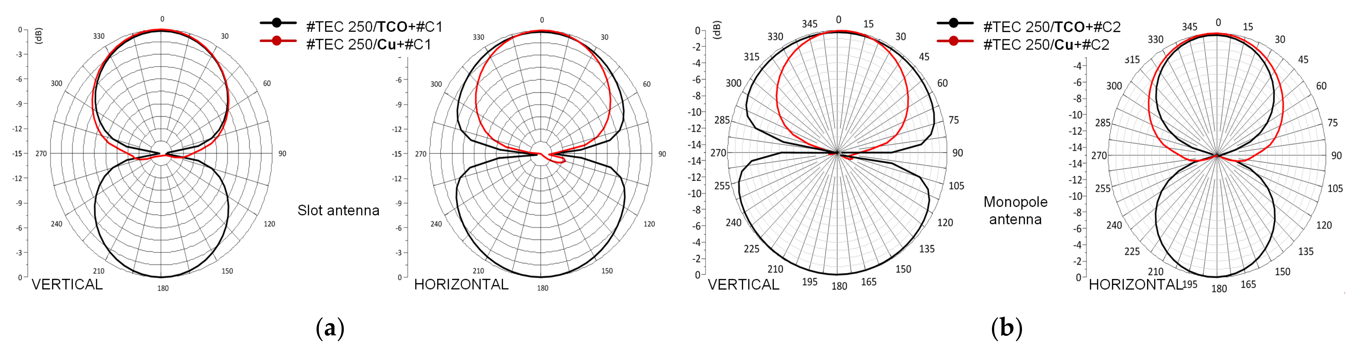
3.2. Antenna with Reflector Introduced into the Glazing Unit

3.2.1. Antenna Design without Own Reflector

The considerations regarding the influence of the TCO layer on the RFID antenna efficiency (Section 2.3) were also extended to other arrangements. The main concern in this instance was not to interfere with the glass/laminate structure, that is, not to remove the TCO layer. The presence of a thin functional layer was taken into consideration in the numerical model. Based on the previously obtained results, only two layers of the dielectric, separated by a layer of air, were considered. The first layer was the pane used in the glazing unit, but fully coated with TCO on the opposite side of the antenna, and the second layer was the substrate of the RFID sensor. The model excluded the unit frame because its impact can be effectively eliminated by selecting the appropriate spatial separation (Section 3.1.3).
Two new antenna patterns #C1 and #C2, presented in Figure 21, were proposed for the research. They can operate in close proximity of the TCO layer. The first of the proposed structures (#C1) was the so-called slot antenna. It consisted of a plane of ground in which an appropriately sized hole was cut. An additional impedance matching loop for the AMS SL900A chip was included in the design. In addition, a place for connecting the DC block was provided as the radiator was short-circuited to the ground. The second construction #C2 was the classical monopole. Its radiator was made in the form of an expanding microstrip line terminated with a radiating element.
The numerical models were prepared in two versions for the different types of glass, Stopray Vision-50 or NSG TEC 250, marked respectively: #SV-50+#C1, #SV-50+#C2, #TEC 250+#C1, and #TEC 250+#C2.
The radiation efficiency of both antenna designs was very low (Figure 22), despite a correctly calculated model. This is due to the closeness of the TCO layer that is located directly under the radiator. In this case, the communication between the RFID sensor and the RWD can be impossible even for a small read range.
It is also worth paying attention to the directional diagrams of the radiation pattern. The back lobes were strongly suppressed in the model with the Stopray Vision-50 pane (dark line in Figure 23), and the diagram was directional. In contrast, the diagram of the model with an NSG TEC 250 pane was similar to the radiation characteristics of a half-wave dipole. The difference was caused by the conductivity of the TCO layer.
Finally, if the conductivity of the coating is high (5 Ω/□ for Stopray Vision-50 pane), then the functional layer works as a reflector and most of the radiated energy is concentrated in the main beam. In the case of the low conductivity (300 Ω/□ for NSG TEC 250) pane, the layer works as an absorber, slightly suppressing electromagnetic waves.

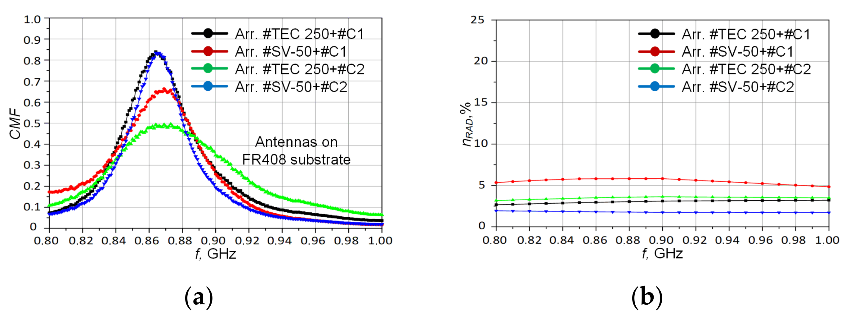
3.2.2. Reflector under TCO Layer

The influence of the thin functional layer can be eliminated by using a reflector inside the structure of the glazing unit (on the inner side of the pane, opposite to the antenna radiator). A conductive material, such as 18 µm thick copper plate, can be used for this purpose. In consequence, the radiation pattern becomes strongly directional and the maximum value of the power transfer coefficient was significantly increased (Figure 24), but the antenna operating bandwidth (defined for CMF in the range from 0.5 to 1) was narrowed. In addition, an improvement in the propagation properties can be observed and is manifested in particular by a significant increase in the radiation efficiency (Figure 24a). The copper layer, with better conductivity than the TCO, resulted in a further reduction of the antenna’s back radiation (Figure 25)—in the case of the SV-50 pane, the directional diagrams were almost the same for the models with the Cu and TCO component. Significant differences were visible in the model with the TEC 250 (Figure 25) because of the low conductivity of the functional layer (please compare with Figure 23). In the case of a monopole, there is no significant improvement in the radiation efficiency (Figure 24b). This is due to the fact that the open antenna is more sensitive to harsh environmental conditions than the slot antenna.
The proposed idea of an additional Cu conductive layer as the reflector enabled attenuation of the influence of TCO (or the heating coatings, as well as any other thin layers that are used in PV cells), and design of the antenna system with well-matched impedance. However, the problem of preparing the numerical model of the radiation structure placed on the glass substrate, especially under the PV module components, needs to be overcome. Where the type of pane is changed, from which the target glazing unit is built, it is necessary also to change the geometrical dimensions of the proposed RFID antenna. Furthermore, in order to obtain convergence of the numerical calculations, the εr parameter of the used materials needs to be accurately determined.

4. Conclusions

The main conclusion from the research undertaken is that the dielectric and mechanical (e.g., thickness) parameters of the glass panes used in the construction of a glazing unit have a significant influence on the impedance properties of the radiation circuit in the RFID sensors. In order to achieve the assumed level of impedance matching between the antenna and the chip, it is necessary to know the exact values of the parameters and to introduce them correctly into the numerical calculations. However, only little information on the properties of the material used was obtainable from the scientific literature, and the manufacturers’ datasheets and notes did not provide details on the desired parameters of the glass, functional layer, frame of units, etc.
Designers can seek to adapt RFID tag constructions dedicated to operation in harsh environments (close to metal or glass), or for implementation in automotive applications. However, in the known typical designs of transponders, the RFID chip position inside the structure of the antenna circuits makes it impossible to feed measured signals to the acquisition blocks. The problem becomes complicated when the transponder needs to operate in a semi-passive mode, which is the case when designing the RFID sensors for PV applications. Moreover, since the semi-passive chip cannot operate with the matching circuit in the form of a short-circuited loop, the special construction of the antenna has to be considered. However, given the state of the art, the authors propose utilizing the benefits gained from hard-tag construction with the reflector of electromagnetic waves. An unquestionable advantage in this case is the potential for fixing the RFID antenna system on the surface of the outer pane of the glazing unit. There is no need to interfere with the structure of the unit and it allows implementation of the RFID-sensor at any stage of production.
Generally, if the UHF antenna of the typical RFID sensor is placed directly above the conductive layer (i.e., heating, TCO layer) it results in a significant decrease in its radiation efficiency. It is observed as a drop in energy gain, a decrease in the amount of harvested supply power in the chip and, finally, as a reduction in the read/write range. This negative impact can be overcome, but the RFID antenna needs to be designed very precisely with great attention to the values of the parameters of the materials used in the structure of the glazing unit. In consequence, in such cases, the RFID sensor is not a universal device.
Therefore, the article has proposed some minor active glazing unit modifications, such as removing the conductive layer under the radiation circuit, or immunising the antenna operation by using an additional copper plate. The possibility of establishing radio communication from both sides of the active glazing unit (from inside and outside of the building) is a significant advantage of the first approach. On the basis of the simulation results, it can be clearly stated that the omission of the TCO layer and the metal frame in numerical models does not significantly affect the calculation accuracy, provided that the spatial separation is introduced.
The proposed idea of the additional copper conductive reflective plate allows for attenuating the influence of the conductive layer and the design of an antenna system with well-matched impedance. However, the problem of preparing the numerical model of the radiation structure placed on the glass substrate has to be overcame. In the case of changing the type of pane, from which the target glazing unit is built, it is necessary also to change the geometrical dimensions of the proposed RFID antenna. Furthermore, in order to obtain convergence of the numerical calculations, the dielectric parameters of the materials used need to be accurately determined.
Moreover, the impact of the PV module components has been considered. The best solutions to the problem are to maintain the distance or to apply the reflector under the antenna; removing the window in the TCO layer or PV components is not recommended due to technological difficulties, although is possible. These solutions will work for all commercial PV modules that are fabricated in the Ist, IInd, and IIIrd generation, and that are not transparent. These PV modules cannot cover the entire surface of the active glazing unit due to the need to transmit sunlight inside the building. The problem arises when transparent PV nano-layers are used. Since the technology is not widely available, the dielectric parameters of the nano-layers and the means of current outputs in a new PV module are unknown. As it is a potential solution, developments in this technology need to be pursued, and research in this area is to be welcomed.

Author Contributions

Conceptualization, P.J.-M. and C.C.; methodology, M.W.; software, W.L. and M.C.; validation, P.J.-M. and C.C.; formal analysis, P.J.-M. and M.W.; investigation, M.C. and P.P.; resources, W.L. and M.C.; data curation, W.L. and M.C.; writing—original draft, M.W.; writing—review & editing, M.W.; visualization, W.L. and M.C.; supervision, P.J.-M.; project administration, M.W.; funding acquisition, M.W. All authors have read and agreed to the published version of the manuscript.

Funding

This research paper was developed under the project financed by the Minister of Education and Science of the Republic of Poland within the “Regional Initiative of Excellence” program for years 2019–2022. Project number 027/RID/2018/19, amount granted 11 999 900 PLN.

Institutional Review Board Statement

Not applicable.

Informed Consent Statement

Not applicable.

Data Availability Statement

All calculated and measured data will be provided upon request to the correspondent authors by email with appropriate justification.

Conflicts of Interest

The authors declare no conflict of interest. The funders had no role in the design of the study; in the collection, analyses, or interpretation of data; in the writing of the manuscript, or in the decision to publish the results.

Appendix A

In the paper, the authors consider the influence of active glazing unit components on the efficiency of RFID antenna. If the distance between the radiation circuit and the components is sufficient then this impact can be ignored. Otherwise, if the RFID sensor is to be placed close to the photovoltaic cells then their structure has to be taken into consideration in the antenna synthesis process. A PV cell can be considered as a spatial structure composed of several layers; then the dielectric parameters need to be determined for each material used in the photovoltaic stack. Based on the data gathered, it is possible to build a numerical model using specialized simulation software, as well as to estimate the influence of the construction materials on the electromagnetic field distribution. For example, in the case of dye-sensitized solar cell DSSC, approximate values of electrical parameters can be found in the publication [30] and are summarized in Table A1. The presence of metal and fluids (electrolyte) in the 3rd generation PV cell strongly affects the impedance parameters and the energy efficiency of RFID antennas. Therefore, locating the antenna system of an RFID sensor on the surface, or in the close vicinity of DSSC, requires the use of a special design, dedicated to operation in difficult environmental conditions (e.g., with an additional reflector under the radiator).
Table A1. Selected parameters of the material used in DSSC [31,32,33,34].
Layerεrδ, S/mThickness
Glass6,7N/A2 mm
Transparent conductive oxides ITON/A10−6600 nm
Transparent semi-conductive oxides TiO285N/A10 µm
ElectrolyteN/A3·10−40,4 mm
Catalyst layer, PtN/A9,66·10−65 nm

Appendix B

In order to conduct an effective analysis of RFID antenna performance based on the results obtained from the numerical calculations, two aspects should be taken into account: (a) impedance, (b) propagation. In the first case, special attention should be paid to the power transfer factor, which describes the amount of energy passing from the antenna to the transponder chip. This parameter is also referred to as CMF (conjugate match factor). It is a numerical measure of the impedance matching of two components and can be determined from the relationship [7]:
τ = 4 Re Z T A Re Z T C Re Z T A + Z T C 2 + Im Z T A + Z T C 2
where ZTA means antenna impedance and ZTC means chip impedance. The components are matched when CMF = 1 (τ = 1) which implies full coupling of both impedances ZTA = ZTC*).
When the propagation aspects are considered, then the radiation efficiency ηRAD, should be taken into account. This parameter is determined from the dependence:
η R A D = P r a d i a t i o n P i n p u t
as the ratio of power radiated Pradiation and delivered Pinput to the antenna. The value of 100% means that the whole energy is radiated, 0% means lack of radiation.

Appendix C

Every real capacitor can be represented by an RLC equivalent with capacitance C0 serial resistance RS (ESR—equivalent series resistance), serial inductance LS (ESI—equivalent series inductance) and parasitic parallel capacitance CP that is related to the parallel resonant frequency fPR (Figure A1a).
Figure A1. DC block: (a) Equivalent of real capacitor; (b) Fragment of an exemplary simulated RFID antenna with DC block.
Energies 14 06632 g0a1
The serial resonant frequency fSR of the capacitor is described by the formula:
f S R = 1 2 π L S C 0
The capacitor reactance is close to zero and the impedance is equal to the serial resistance RS at this frequency. On the basis of (C1), the capacitance can be determined for which the influence of the capacitor on the antenna performance is negligible. The impedance equivalent is described by the relationship:
Z C A P = ( R s ) 2 + ( X L X C ) 2
where, XL, XC means values of the reactance.
The impedance module of an exemplary capacitor (e.g., 100 pF) with a 1 GHz self-resonance [35,36] is shown in Figure A2a. This passive element shows a capacitive nature below the fSR frequency (the graph shows a hyperbolic curve), and an inductive characteristic above this point (a linear segment of the graph). The selection of the parasitic parallel resonance is another important aspect when looking for a capacitor for the DC block. The frequency fPR is determined by the value CP in the equivalent circuit. The RF signal attenuation caused by the DC Block is visible in the plot of parameter S21 (Figure A2b). If the capacitor is to be used in the antenna of an RFID sensor, the value of this parameter should not exceed a few tenths of dB in the considered operating band.
Figure A2. Characteristics of 100 pF capacitor—example: (a) Impedance ZCAP; (b) S21.
Energies 14 06632 g0a2
The ceramic MLCC capacitors should be used in the UHF radiofrequency band. They are designated as NP0 and C0G according to the used dielectric. The capacitance of 33–68 pF is usually used in the frequency band of 860–915 MHz. Additionally, the capacitor should have a sufficiently large value of Q factor when it is intended to be used as the DC block. The Q parameter can be determined by the dependence:
Q = X C X L E S R
It is also desirable that the fSR frequency should be slightly higher than the operating frequency [37,38].
Considering all the described requirements and commercially available products, limited additionally by the preferred number of values, the MULTICOMP MC0603N560J500CT capacitor of 56 pF, in the housing 0603 [39], was selected for the considered investigations on the RFID sensor. The simulation of an exemplary structure was carried out in order to check the influence of the selected capacitor on the impedance of the RFID antenna. The test setup consisted of an antenna on a dielectric substrate ISOLA FR408, placed on a low-iron laminate with a passive copper reflector at the bottom. The calculations were performed for models with and without the DC block (Figure A1b).
Based on the graphs (Figure A3), a negligible effect of the capacitor on the antenna impedance was observed. Slight differences in the CMF values may result from the method of preparing the model in the numerical software. A new port is defined instead of the slot in the antenna path in order to represent the DC block. It may have a minor effect on the value of the calculated impedance. It should also be noted that the value of the capacitance was calculated for the 866 MHz frequency and selected with some uncertainty from the available preferred series.
Figure A3. Influence of DC block on RFID antenna parameters: (a) Impedance ZTA; (b) CMF.
Energies 14 06632 g0a3

References

  1. Finkenzeller, K. RFID Handbook—Fundamentals and Applications in Contactless Smart Cards, Radio Frequency Identification and Near-Field Communication, 3rd ed.; Wiley: West Sussex, UK, 2010. [Google Scholar]
  2. Costa, F.; Genovesi, S.; Borgese, M.; Michel, A.; Dicandia, F.A.; Manara, G. A Review of RFID Sensors, the New Frontier of Internet of Things. Sensors 2021, 21, 3138. [Google Scholar] [CrossRef] [PubMed]
  3. Erman, F.; Hanafi, E.; Lim, E.-H.; Wan Mohd Mahyiddin, W.A.; Harun, S.W.; Umair, H.; Soboh, R.; Makmud, M.Z.H. Miniature Compact Folded Dipole for Metal Mountable UHF RFID Tag Antenna. Electronics 2019, 8, 713. [Google Scholar] [CrossRef] [Green Version]
  4. Chung, Y.; Berhe, T.H. Long-Range UHF RFID Tag for Automotive License Plate. Sensors 2021, 21, 2521. [Google Scholar] [CrossRef] [PubMed]
  5. El Khamlichi, M.; Alvarez Melcon, A.; El Mrabet, O.; Ennasar, M.A.; Hinojosa, J. Flexible UHF RFID Tag for Blood Tubes Monitoring. Sensors 2019, 19, 4903. [Google Scholar] [CrossRef] [PubMed] [Green Version]
  6. Franchina, V.; Ria, A.; Michel, A.; Bruschi, P.; Nepa, P.; Salvatore, A. A Compact UHF RFID Ceramic Tag for High-Temperature Applications. In Proceedings of the 2019 IEEE International Conference on RFID Technology and Applications (RFID-TA), Pisa, Italy, 25–27 September 2019; pp. 480–483. [Google Scholar] [CrossRef]
  7. Jankowski-Mihułowicz, P.; Węglarski, M. Definition, Characteristics and Determining Parameters of Antennas in Terms of Synthesizing the Interrogation Zone in RFID Systems. In Radio Frequency Identification; Crepaldi, P.C., Pimenta, T.C., Eds.; IntechOpen: London, UK, 2017; Chapter 5; pp. 65–119. ISBN 978-953-51-3630-9. [Google Scholar] [CrossRef] [Green Version]
  8. Khadka, G.; Hwang, S.-S. Tag-to-Tag Interference Suppression Technique Based on Time Division for RFID. Sensors 2017, 17, 78. [Google Scholar] [CrossRef] [PubMed] [Green Version]
  9. ISO/IEC 18000-63. Information Technology—Radio Frequency Identification for Item Management—Part 63: Parameters for Air Interface Communications at 860 MHz to 960 MHz Type C; International Organization for Standardization: Geneva, Switzerland, 2015. [Google Scholar]
  10. GS1 EPCglobal. EPC Radio-Frequency Identity Protocols Generation-2 UHF RFID; Specification for RFID Air Interface Protocol for Communications at 860 MHz–960 MHz; ver. 2.0.1; EPCglobal: Brussels, Belgium, April 2015. [Google Scholar]
  11. ETSI EN 302 208. Radio Frequency Identification Equipment Operating in the Band 865 MHz to 868 MHz with Power Levels up to 2 W and in the Band 915 MHz to 921 MHz with Power Levels up to 4 W; Harmonised Standard Covering the Essential Requirements of Article 3.2 of the Directive 2014/53/EU, v.3.1.1; European Telecommunications Standards Institute: Sophia-Antipolis, France, 2016. [Google Scholar]
  12. Code of Federal Regulations. Title 47. Telecommunication. Part 15.247 Operation within the bands 902–928 MHz, 2400–2483.5 MHz, and 5725–5850 MHz; Published by the Office of the Federal Register National Archives and Records Administration as a Special Edition of the Federal Register: Washington, DC, USA, October 2020. [Google Scholar]
  13. Marrocco, G. The art of UHF RFID antenna design: Impedance-matching and size-reduction techniques. IEEE Antennas Propag. Mag. 2008, 50, 66–79. [Google Scholar] [CrossRef] [Green Version]
  14. Węglarski, M.; Jankowski-Mihułowicz, P.; Chamera, M.; Dziedzic, J.; Kwaśnicki, P. Designing Antennas for RFID Sensors in Monitoring Parameters of Photovoltaic Panels. Micromachines 2020, 11, 420. [Google Scholar] [CrossRef] [PubMed] [Green Version]
  15. Hussain, M.; Amin, Y.; Lee, K.-G. A Compact and Flexible UHF RFID Tag Antenna for Massive IoT Devices in 5G System. Sensors 2020, 20, 5713. [Google Scholar] [CrossRef] [PubMed]
  16. Phatarachaisakul, T.; Pumpoung, T.; Phongcharoenpanich, C. Dual-band RFID tag antenna with EBG for glass objects. In Proceedings of the IEEE 4th Asia-Pacific Conference on Antennas and Propagation (APCAP), Bali, Indonesia, 30 June–3 July 2015; pp. 199–200. [Google Scholar] [CrossRef]
  17. Lu, J.H.; Wu, J.J. UHF band RFID tag antenna mounted on glass objects. In Proceedings of the IEEE Asia Pacific Microwave Conference, Singapore, 7–10 December 2009; pp. 622–624. [Google Scholar] [CrossRef]
  18. Lu, J.H.; Chang, B.S. Planar Compact Square-Ring Tag Antenna with Circular Polarization for UHF RFID Applications. IEEE Trans. Antennas Propag. 2017, 65, 432–441. [Google Scholar] [CrossRef]
  19. Pan, T.; Zhang, S.; He, S. Compact RFID Tag Antenna with Circular Polarization and Embedded Feed Network for Metallic Objects. IEEE Antennas Wirel. Propag. Lett. 2014, 13, 1271–1274. [Google Scholar] [CrossRef]
  20. Lukas, I.J.; Qing, X.; Chen, Z.N.; Alphones, A. UHF omnidirectional bent dipole antenna for item-level RFID applications. In Proceedings of the IEEE Antennas and Propagation Society International Symposium, San Diego, CA, USA, 5–11 July 2008; pp. 1–4. [Google Scholar] [CrossRef]
  21. Kaiwen, K.T.; Qing, X.; Goh, C.K.; Zhu, L. A UHF omni-directional RFID antenna. In Proceedings of the IEEE Antennas and Propagation Society International Symposium, Toronto, ON, Canada, 11–17 July 2010; pp. 1–4. [Google Scholar] [CrossRef]
  22. Jankowski-Mihułowicz, P.; Lichoń, W.; Pitera, G.; Węglarski, M. Determination of the Material Relative Permittivity in the UHF Band by Using T and Modified Ring Resonators. Int. J. Electron. Telecommun. 2016, 62, 129–134. [Google Scholar] [CrossRef] [Green Version]
  23. ISOLA. FR408 High Performance Laminate and Prepreg, Data Sheet; Isola Group: Chandler, AZ, USA, 2018. [Google Scholar]
  24. DuPont. Pyralux LF Copper-Clad Laminates—Flexible Composites, Data Sheet, H-73244-5 06/12, USA; DuPont Electronic Technologies: Wilmington, DE, USA, 2012. [Google Scholar]
  25. Pilkington. NSG TEC; Datasheet; Pilkington: Deutschland, AG, USA, 2018. [Google Scholar]
  26. Krupka, J.; Gregory, A.P.; Rochard, O.C.; Clarke, R.N.; Riddle, B.; Baker-Jarvis, J. Uncertainty of complex permittivity measurements by split-post dielectric resonator technique. J. Eur. Ceram. Soc. 2001, 21, 2673–2676. [Google Scholar] [CrossRef]
  27. Jankowski-Mihułowicz, P.; Węglarski, M.; Lichoń, W. A Procedure for Validating Impedance Parameters of HF/UHF RFID Transponder Antennas. In Methods and Techniques of Signal Processing in Physical Measurements; Hanus, R., Mazur, D., Kreischer, C., Eds.; MSM2018. Lecture Notes in Electrical Engineering; Springer: Cham, Switzerland, 2019; Volume 548, pp. 101–118. ISBN 978-3-030-11186-1. [Google Scholar] [CrossRef]
  28. Ali, W.; AI-Charchafchi, S.H. Using Equivalent Constant to Simplify the Analisys of Patch Microstrip Antenna with Multi Layer Substrates. In Proceedings of the IEEE Antennas and Propagation Society International Symposium, Atlanta, GA, USA, 21–26 June 1998. [Google Scholar] [CrossRef]
  29. Mentor Graphics: IE3D User Manual; Mentor Graphics: Wilsonville, OR, USA, 2012.
  30. O’Conchubhair, O.; McEvoy, P.; Ammann, M.J. Dye-Sensitized Solar Cell Antenna. IEEE Antennas Wirel. Propag. Lett. 2016, 16, 352–355. [Google Scholar] [CrossRef]
  31. SCHOTT. D263 Thin Glass, Technical Documentation; Schott AG: Mainz, Germany, 2013. [Google Scholar]
  32. Material: Indium Tin Oxide (ITO). Available online: www.mit.edu/~6.777/matprops/ito.htm (accessed on 20 November 2017).
  33. Zhu, L.U.; Zhang, L.D.; Fang, Q. X-ray photoelectron spectroscopystudy of ZrO2/TiO2/Si stack. Appl. Phys. Lett. 2007, 91, 17. [Google Scholar] [CrossRef]
  34. Jovanovski, V.; Stathatos, E.; Orel, B.; Lianos, P. Dye-sensitized solarcells with electrolyte based on a trimethoxysilane-derived ionic liquid. Thin Solid Films 2006, 511, 634–637. [Google Scholar] [CrossRef]
  35. American Technical Ceramics. Capacitors in Broadband Applications; Application Note, ATC # 001-951, Rev. D 1/05; American Technical Ceramics: Huntington Station, NY, USA, 2001. [Google Scholar]
  36. American Technical Ceramics. Capacitors in Coupling and DC Block Applications, Circuit Designer’s Notebook; Document #001-927, Rev. E, 1/05; American Technical Ceramics: Huntington Station, NY, USA, 2001. [Google Scholar]
  37. Semtech. RF Design Guidelines: PCB Layout Circuit Optimization; Application Note, AN 1200.04; Semtech: Camarillo, CA, USA, 2006. [Google Scholar]
  38. Infineon Technologies. ESD Protection for RF Antennas Using Infineon ESD0P4RFL and ESD0P2RF; Application Note, Rev. 1.0; Infineon Technologies: Neubiberg, Germany, 2008. [Google Scholar]
  39. MULTICOMP. General Purpose Multilayer Ceramic Capacitors—4 to 100V (NP0, X5R, X7R & Y5V Dielectrics), Data Sheet; Farnell: Chicago, IL, USA, 2018. [Google Scholar]
Figure 1. Active glazing unit in modern multi-storey buildings: (a) Spatial separation between RFID sensor and construction elements; (b) Idea of using window in the TCO or heating layer for delivering system electromagnetic field to antenna of RFID sensor.
Energies 14 06632 g001
Figure 2. Laboratory stand for measuring dielectric parameters: (a) Hardware; (b) Software.
Energies 14 06632 g002
Figure 3. Measurements of RFID antennas: (a) PCB substrate on low-iron laminate; (b) Flexible substrate in free space, plastic net under the sample; (c) Flexible substrate on low-iron laminate; (d) Numerical model (Lx, Wx, H, G—dimensions).
Energies 14 06632 g003
Figure 4. Impedance (Re—realism, Im—imaginalism) of RFID antenna on substrate: (a,c,e) ISOLA FR408; (b,d,f) DuPont Pyralux, obtained for: (a,b) quasi-free space conditions; (c,d) stack with low-iron laminate sample; (e,f) stack with low-iron glass sample.
Energies 14 06632 g004
Figure 5. Designs of RFID antenna with short-circuited arms: (a) Design #A1; (b) Design #A2; (c) Sample under tests; (d) Numerical model of #A2 design (Lx, Wx, H—dimensions).
Energies 14 06632 g005
Figure 6. Impedance of RFID antenna: (a) Design #A1 on low-iron laminate; (b) Design #A2 on low-iron laminate; (c) Design #A2 on low-iron glass.
Energies 14 06632 g006aEnergies 14 06632 g006b
Figure 7. CMF of RFID antenna: (a) Design #A1 on low-iron laminate; (b) Design #A2 on low-iron laminate; (c) Design #A2 on low-iron glass.
Energies 14 06632 g007
Figure 8. Impedance of RFID antenna: (a) Design #A2 on both sides of low-iron glass; (b) Design #A2 on NoName glass.
Energies 14 06632 g008aEnergies 14 06632 g008b
Figure 9. Impedance of RFID antenna: (a) #A1; (b) #A2. Thin layer of air (0.4 mm) between the FR408 laminate and the glass surface is included.
Energies 14 06632 g009
Figure 10. TCO impact on impedance of RFID antenna made on FR408 and placed on Stopray Vision-50 glass.
Energies 14 06632 g010
Figure 11. Impedance of RFID antenna located in different arrangements (a) ISOLA FR408; (b) DuPont Pyralux.
Energies 14 06632 g011
Figure 12. Design of RFID antenna with reflector under radiator: (a) Sample; (b) Measurement stand.
Energies 14 06632 g012
Figure 13. Impedance of RFID monopole antenna: (a) Calculations and measurements comparison; (b) Influence of glazing unit components; (c) Negative impact of changes in geometric dimensions of antenna.
Energies 14 06632 g013
Figure 14. Model of RFID antenna for bidirectional communication: (a) Arrangement #SV-50 with Stopray Vision-50; (b) Arrangement #TEC 250 with NSG TEC 250 (Table 1); (c) Antenna design #B1; (d) Antenna design #B2.
Energies 14 06632 g014
Figure 15. Parameters of RFID antennas: (a) CMF; (b) Radiation efficiency nRAD; (c) Radiation pattern (f0 = 866 MHz) of antenna #B2 in the arrangement of #SV-50; (d) Radiation pattern (f0 = 866 MHz) of antenna #B2 in the arrangement of #TEC 250. The radiation pattern of antenna #B1 is very similar.
Energies 14 06632 g015
Figure 16. Visualization of considered cases of RFID sensor and TCO layer localization: (a) Initial position; (b) Separation x = 10 mm, 20 mm, 30 mm, 40 mm, 50 mm.
Energies 14 06632 g016
Figure 17. CMF and radiation efficiency nRAD vs. separation distance between TCO and antenna radiator in arrangements: (a) #TEC 250+#B1; (b) #SV-50+#B1; (c) #TEC 250+#B2; (d) #SV-50+#B2.
Energies 14 06632 g017aEnergies 14 06632 g017b
Figure 18. Considered cases of RFID antenna and frame unit arrangements: (a) Separation x = 10 mm, 20 mm, 30 mm, 40 mm, 50 mm, 60 mm, 70 mm, 80 mm; (b) RFID antenna on the inner pane No.1 (c) RFID antenna on the outer pane No.2.
Energies 14 06632 g018
Figure 19. CMF and radiation efficiency nRAD vs. separation distance between unit frame and antenna radiator in arrangements: (a) No.1+#B1; (b) No.2+#B1; (c) No.1+#B2; (d) No.2+#B2.
Energies 14 06632 g019
Figure 20. Directional diagrams of radiation pattern vs. separation distance between unit frame and antenna radiator in arrangements (f0 = 866 MHz): (a) No.1+#B1; (b) No.2+#B1; (c) No.1+#B2; (d) No.2+#B2.
Energies 14 06632 g020
Figure 21. RFID antenna: (a) Slot antenna #C1; (b) Monopole antenna #C2; (c) Antenna sample under tests.
Energies 14 06632 g021
Figure 22. Parameters of RFID antennas: (a) CMF; (b) Radiation efficiency nRAD.
Energies 14 06632 g022
Figure 23. Vertical and horizontal directional diagrams (f0 = 866 MHz): (a) Slot antenna #C1; (b) Monopole antenna #C2.
Energies 14 06632 g023
Figure 24. CMF and radiation efficiency nRAD when modelling with TCO or Cu layer: (a) Slot antenna #C1; (b) Monopole antenna #C2.
Energies 14 06632 g024aEnergies 14 06632 g024b
Figure 25. Vertical and horizontal directional diagrams (f0 = 866 MHz): (a) Slot antenna #C1; (b) Monopole antenna #C2.
Energies 14 06632 g025
Table 1. Dielectric parameters of selected glass samples and transponder substrates.
Pos.Name of Dielectric MaterialThickness, mmεrtgδ
1.Glass: Low Iron1.927.009.290·10−3
2.Laminate: Low Iron + SKC EVA sheet + Low Iron4.246.619.423·10−3
3.Pikligton NSG TEC 2503.216.89.000·10−3
4.AGC Stopray Vision-505.8645.09.000·10−3
5.ISOLA FR4080.514.449.605·10−3
6.DuPont Pyralux LF9150R0.1253.559.200·10−3
7.ISOLA IS-680-300 microwave 1.5473.083.000·10−3
Pos.Name of Functional LayerThickness, µmR, Ω/δ,S/m
1TCO (NSG TEC 250)0.5300
2TCO (Stopray Vison-50)0.55
3Cu clad (FR408)18 4.8·108
4Cu clad (Pyralux LF9150R)35 4.8·108
Publisher’s Note: MDPI stays neutral with regard to jurisdictional claims in published maps and institutional affiliations.

