Article

A Modular Multilevel Converter with an Advanced PWM Control Technique for Grid-Tied Photovoltaic System

1
Department of Electronics & Telecommunication Engineering, Rajshahi University of Engineering & Technology, Rajshahi 6204, Bangladesh
2
School of Electrical, Computer and Telecommunications Engineering, University of Wollongong, Wollongong, NSW 2522, Australia
*
Authors to whom correspondence should be addressed.
Energies 2021, 14(2), 331; https://doi.org/10.3390/en14020331
Submission received: 7 December 2020 / Revised: 30 December 2020 / Accepted: 5 January 2021 / Published: 8 January 2021

Abstract

:
Due to global warming and shortage of fossil fuels, the grid-connected solar photovoltaic (PV) system has gained significant popularity all over the world. The modular multilevel cascaded (MMC) inverter is the natural choice for step-up transformer and line filter less direct medium voltage grid integration of solar PV systems. However, power quality and loss are the important issues while connecting the PV system to the medium voltage grid through MMC inverter. Modulation technique is the key to maintain output power quality, e.g., total harmonic distortion (THD) and to ensure low switching and conduction losses. In this paper, an advanced modulation technique named “triangle saturated common mode pulse width modulation (TSCMPWM)” control is proposed for a 3-phase 5-level MMC inverter-based grid-tied PV system. Compared to traditional modulation techniques, the proposed TSCMPWM control offers the lowest voltage THD as well as lower inverter power losses. Performance of the proposed modulation technique is evaluated in MATLAB/Simulink environment and tested with a reduced scale prototype test platform. Both simulation and experimental results show the effectiveness of the proposed modulation technique.

1. Introduction

To mitigate the increasing energy demand without affecting the environment, the renewable energy sources such as solar, oceanic wave, and wind are being considered as the alternative source of energy all over the world. Among different renewable power generation systems, solar photovoltaic (PV) system has received significant interest due to a number of features such as cost-effectiveness and technological advancement. The number of installed solar PV power plants in the world are increasing rapidly to replace the traditional fossil fuel-based electrical power plants [1,2]. In grid-connected solar PV plants, inverters play an important role in conversion of electrical energy from DC to AC before feeding the solar power to grid. Due to some special features such as capability to handle high voltage and generate staircase sinusoidal output voltage, the multilevel inverters have gained considerable popularity for their use in step-up transformer and line filter less medium voltage grid integration of solar PV power plants. [3,4]. A wide research has been done by the research community on different types of multilevel inverter topologies. The neutral point clamped (NPC), flying-capacitor (FC), cascaded H-bridge (CHB) and modular multilevel cascaded (MMC) are the basic multilevel inverter topologies used in different industrial applications [5].
Among these basic topologies, MMC has drawn significant attention from the research community for its numerous advantages such as capability to control the internal power flow, ease of implementation, low harmonic distortion in the output voltage, and less maintenance cost [6,7,8,9,10,11]. Due to these attractive features, MMC inverters are increasingly used in various applications including renewable power generation and industrial medium voltage motor drives [12,13].
However, the switching and conduction losses are the limitations of multilevel inverters, which depends mainly on the modulation techniques used to control the solar PV inverter’s semiconductor switching devices [14,15,16]. To improve the power quality of multilevel inverters, a number of modulation techniques have been proposed by the research community in recent decades, as the amount of conduction and switching losses of a multilevel inverter circuit greatly depends upon the switching technique used in the multilevel inverters.
The pulse width modulation (PWM) technique is the most fundamental switching strategy for multilevel inverters, where the gate pulses are mainly generated by comparing the reference signal with a carrier signal of higher frequency. The PWM technique has some advantages such as easy to implement, better performance [17], and limited amount of power loss in the switching devices [18]. Several PWM-based advanced switching techniques have been presented in the literature including sine PWM (SPWM), third harmonic-injected PWM (THPWM), conventional space vector PWM (CSVPWM), sixty-degree PWM (SDPWM), third harmonic sixty-degree PWM (THSDPWM), trapezoidal PWM (TRPWM), third harmonic trapezoidal PWM (THTRPWM), and fifth harmonic trapezoidal PWM (FHTRPWM) [19]. A comparative analysis of the performance of all these traditional switching techniques has been presented in [17]. The THPWM technique has been the most adopted modulation technique among all the traditional PWM modulation techniques based on THD [20]. On the other hand, the CSVPWM technique has been widely applied for better DC bus voltage utilization and flexible control [21,22,23,24]. Although these two techniques provide a good harmonic spectrum, the THPWM technique causes high power losses in the MMC inverters and the practical implementation of the CSVPWM technique is quite complex in case of the MMC inverters [4]. The thirty-degree bus clamping PWM (TDBCPWM) and sixty-degree bus clamping PWM (SDBCPWM) techniques have also gained popularity due to their use in the MMC inverters with low power losses. However, these techniques show poor spectra property [5].
In this paper, an advanced switching strategy is proposed to minimize the voltage and current THDs at the output and reduce the switching and conduction losses of the MMC inverters. The modulating signal of the proposed switching technique is generated by adding a triangular saturated common-mode signal to a pure sinusoidal reference signal. To test the performance, the proposed switching technique is applied to a solar PV system-based grid-connected 3-phase 5-level MMC inverter. The performance (voltage and current THDs and the power losses) of the proposed switching technique is compared with that of the existing modulation techniques such as SPWM, THPWM, CSVPWM, THSDPWM, TDBCPWM, and SDBCPWM. The key features of the proposed modulation technique are:
  • low output voltage THD,
  • low injected grid current THD,
  • low inverter power loss, and
  • high DC bus voltage utilization.
The paper is organized as follows: the MMC inverter-based grid-tied PV system is described in Section 2, existing PWM techniques are described in Section 3, inverter control for grid synchronization is demonstrated in Section 4, the performance evaluation is described in Section 5, experimental validation is described in Section 6, and finally, the conclusion of the paper is in Section 7.

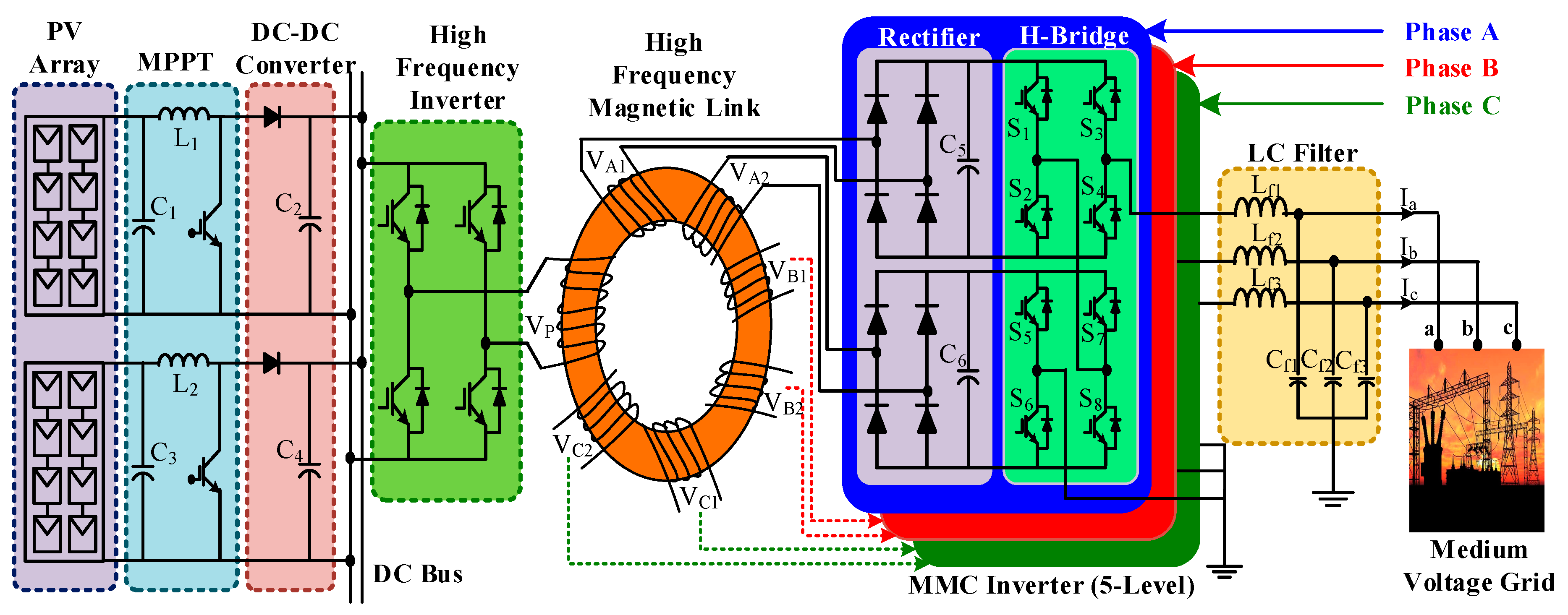
2. The MMC Inverter-Based Grid-Tied PV System

Step-up transformer-less direct medium voltage grid integration of PV array using a 5-level MMC inverter is shown in Figure 1. PV array feeds power to the DC link of the high-frequency inverter through a DC-DC converter. The DC-DC converter ensures maximum power extraction from the PV array and maintain a constant output voltage according to the voltage level of the DC link. The inverter is linked to the high-frequency magnetic-link’s primary winding, and each secondary winding operates via a bridge rectifier as an isolated source connected to the H-bridge cell. The magnetic-link (no voltage step-up) is used to generate isolated and balanced multiple power sources from a single source and to ensure galvanic isolation. THD decreases as the number of MMC inverter levels increases. The rectifier unit rectifies the high-frequency AC voltage to DC voltage, which creates isolated DC source for the H-bridge module. The THD and the switching loss can also be minimized using proper modulation methods for a specific inverter stage. The performance of the proposed modulation technique is analyzed in terms of the THD and the switching loss in the subsequent sections.

3. Existing and Proposed PWM Techniques

3.1. Existing PWM Techniques

The performance of the proposed switching technique is compared with the conventional PWM switching techniques, such as SPWM, THPWM, CSVPWM, THSDPWM, TDBCPWM, and SDBCPWM. The modulating signals of these conventional switching techniques are depicted in Figure 2.
Table 1 depicts the mathematical expressions of existing switching techniques.
The proposed switching technique along with other traditional PWM switching techniques are applied to a 3-phase 5-level MMC inverter modeled in MATLAB/Simulink environment. Figure 3 shows the output line voltage waveforms for the traditional modulation techniques. For each modulation technique, the frequency of the reference signal is kept 50 Hz and as a carrier signal, a 2 kHz phase-shifted triangular signal is used. In the simulations, the modulation index is considered 1. Figure 4 shows the frequency spectrum of the output line voltages for SPWM, THPWM, CSVPWM, THSDPWM, TDBCPWM, and SDBCPWM techniques.
It can be observed from Figure 4 that the THPWM presents the lowest and the SPWM presents the highest THD among all of these traditional switching strategies.
Table 2 shows the inverters line voltage THDs for existing SPWM, THPWM, CSVPWM, THSDPWM, TDBCPWM, and SDBCPWM techniques.

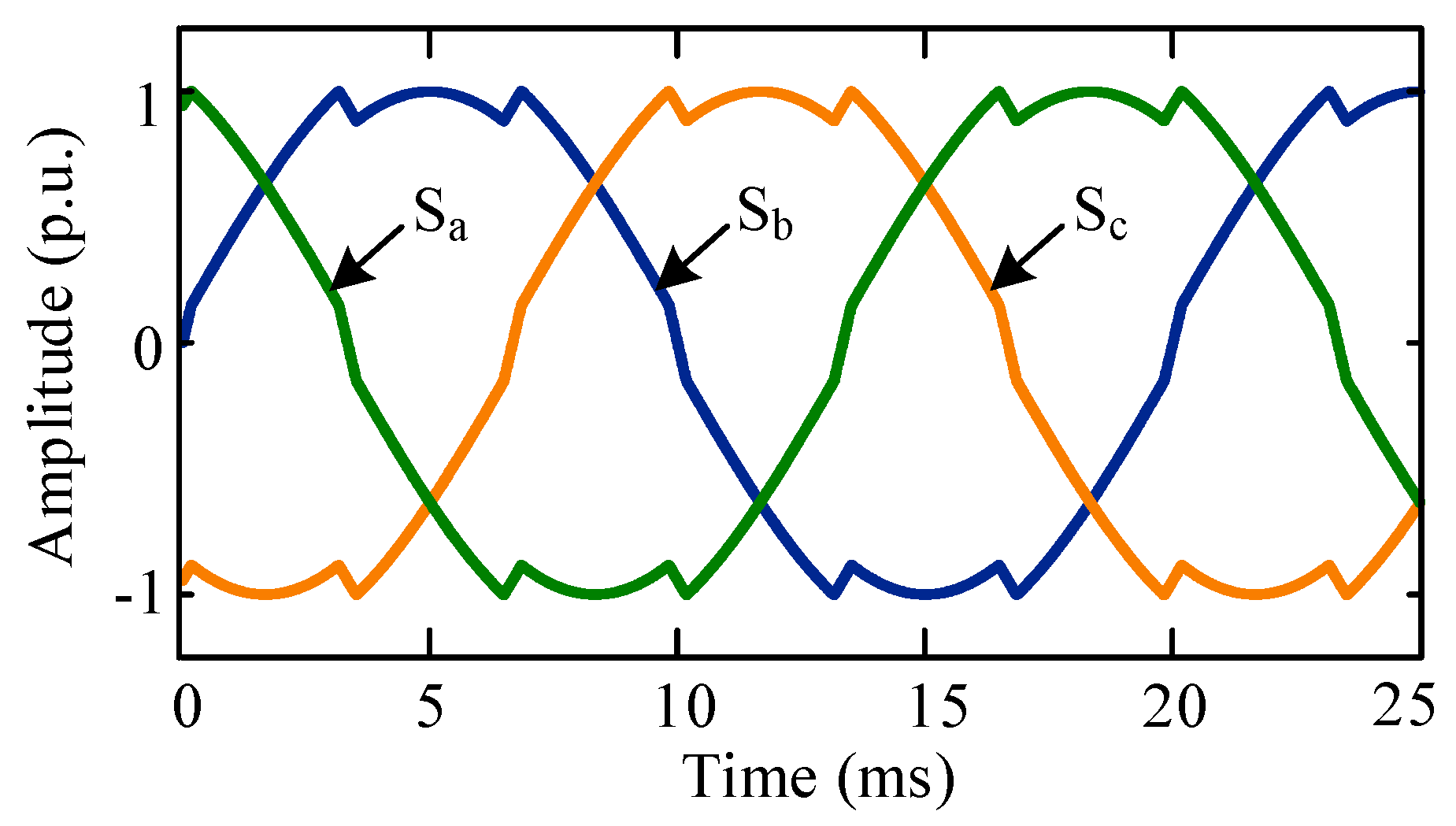
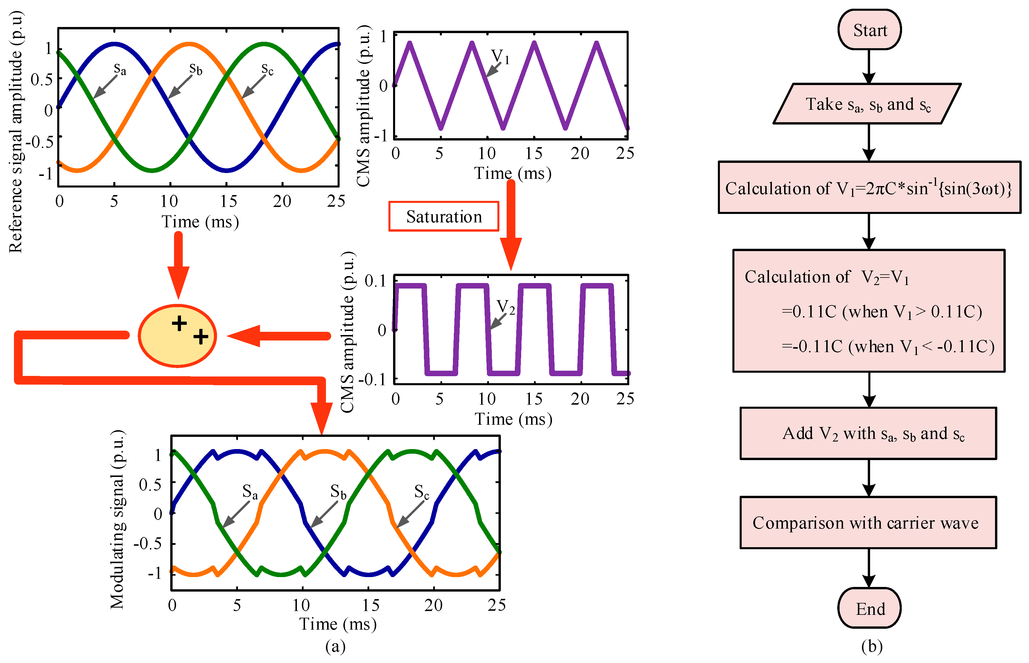
3.2. Proposed PWM Technique

The modulating signal for the proposed triangle saturated common mode-injected PWM technique is depicted in Figure 5. The signal is formed by adding a triangle saturated common mode signal to the three-phase sinusoidal reference signals.
Figure 6a shows the generation of the proposed modulating signal. Here, in this figure, sa, sb, and sc are the three phase sinusoidal signals, and can be expressed by Equations (1)–(3).
s a = A   sin ω t
s b = A   sin ( ω t 120 ° )
s c = A   sin ( ω t + 120 ° ) ,
where A represents the amplitude of the reference signals.
In the next step, a triangular signal, V1 of lower amplitude is generated, which is expressed by Equation (4).
V 1 = 2 π C sin 1 { sin ( 3 ω t ) } ,
where C = 0.77 A .
As depicted in Figure 6a, the common-mode signal, represented by V2, is generated by binding V1 in a region, where the maximum amplitude of the signal is 0.11 C, and the minimum amplitude is −0.11 C. The following equations explains the relation mathematically.
V 2 = V 1
= 0.11 C   ( w h e n   V 1 > 0.11 C )
= 0.11 C   ( w h e n   V 1 < 0.11 C ) .
Finally, the common-mode signal is added to the reference three-phase sinusoidal signals, as expressed in Equations (8)–(10).
S a = A   sin ω t + V 2
S b = A   sin ( ω t 120 ° ) + V 2
S c = A   sin ( ω t + 120 ° ) + V 2 ,
where Sa, Sb, and Sc are the modulating signals of the proposed switching technique for a three-phase MMC inverter.
Figure 6b shows the flowchart for the generation of the proposed TSCMPWM technique. Two phase-shifted carriers (where two carriers are out of phase by 90°) are compared with the modulating signals in the switching schemes and the corresponding gate pulses are produced for the insulated gate bipolar transistors (IGBTs). Figure 7 depicts the procedure of gate pulse generation using the proposed TSCMPWM technique, where a high-frequency triangular carrier signal (2 kHz used in the simulation) is compared with the proposed modulating signal of 50 Hz to generate the gate pulses.
This proposed switching technique is applied to the 3-phase 5-level MMC inverter for PV system, where the values taken for A and C are 1.09 and 0.84, respectively, at modulation index 1. Figure 8 shows the inverter output line voltage and its frequency spectra. The THD of the inverter output line voltage for the proposed technique is 13%, which is lower than the existing six modulation techniques.
The filtered line voltage waveforms and the THD for the proposed TSCMPWM scheme are shown in Figure 9. The filtered line voltage THD of 5-level MMC inverter for TSCMPWM scheme is 0.64%.
Figure 10 depicts the comparative THDs of inverter line voltage for the existing and the proposed TSCMPWM techniques.

4. Inverter Control for Grid Synchronization

For grid-tied operation, the amplitude and frequency of the inverter output voltage need to be synchronized with the grid. The output voltage and frequency of the generator are the leading parameters to synchronize with the grid in the conventional synchronous generator system. The generator synchronizes with the grid at the common coupling point (PCC) after proper matching of amplitude and frequency. Whether or not the synchronization is consistently maintained, it needs to be continuously monitored online. The synchronization condition determines the inverter’s gating signals.
Figure 11 depicts the overall control scheme for the MMC inverter-based PV system utilizing the proposed PWM technique. The reference direct axis component ( I d ) is initially obtained from the dc-link voltage regulator and the reference quadrature axis component ( I q ) is set to zero because of the unity power factor operation of the inverter. The error between the real injected grid currents (Id and Iq) and the reference currents ( I d and I q ) is then passed through the proportional-integral (PI) controllers, and the inverter reference voltage direct axis component ( V d ) and the inverter reference voltage quadrature axis component ( V q ) are determined. After that, the direct and quadrature axis components of the reference inverter voltage are converted into three-phase reference voltages, which are then added to the common mode signal to form the proposed modulating signal. Finally, the modulating signals are compared to the high-frequency carrier signals to produce the gate pulses for the MMC inverter.

5. Performance Evaluation

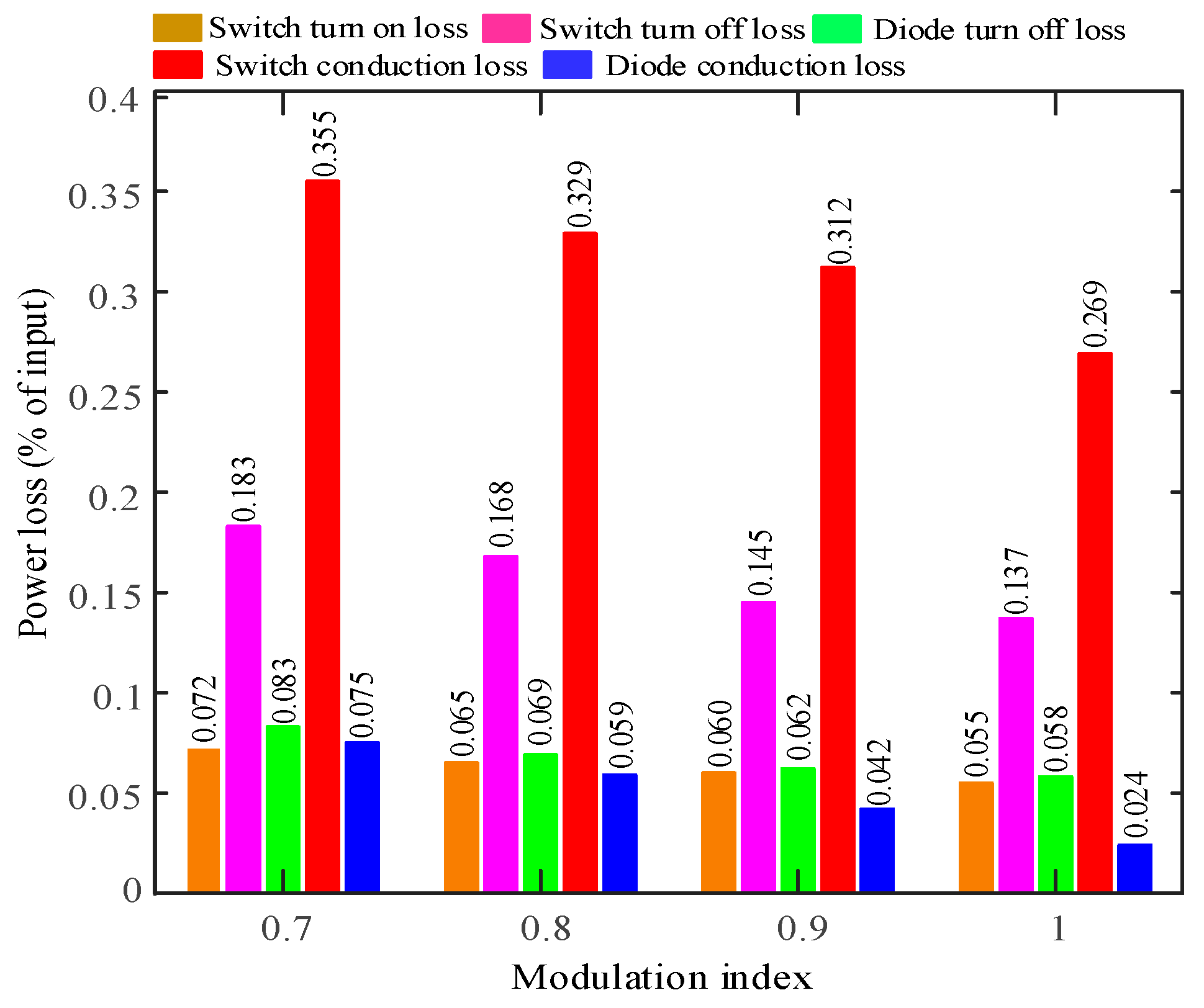
5.1. Loss Evaluation of the MMC Inverter

Inverter losses include switching loss (switch-off, switch-on, and diode turn-off losses) and conduction loss (losses for the switch and the diode conduction). In practice, diode turn-on loss is negligible due to first conducting nature of diode. IGBT module 5SNA 1500E250300 is taken as an example to perform the loss calculation. The equation of the total inverter loss (TIL) can be written as
TIL=Conduction loss (Pcond) + Switching loss (PSL).
Using Equations (12)–(14), the diode conduction loss (Pdcl), switch conduction loss (Pscl), and total conduction loss (Pcon) are calculated [9].
P d c l = 1 2 π 0 2 π [ v F ( t ) i c ( t ) ] d ( ω t )
P s c l = 1 2 π 0 2 π [ v c e ( t ) i c ( t ) ] d ( ω t )
P c o n d = k = 1 N [ P s c l ( k ) + P d c l ( k ) ] ,
where vF, ic, and vce are the voltage drop of antiparallel diode, collector current, and collector–emitter voltage drop, respectively.
For switching loss, switch turn-on loss (Eon) and switch turn-off loss (Eoff) are evaluated using the collector current characteristics curve taken from the datasheet of the IGBT module. The total switching loss (PSL) is calculated using Equation (15). In addition, using diode switch current and reverse recovery characteristics curve of the IGBT, diode switching loss (Erec) is calculated [9]. If N be the number of IGBTs, total diode switching loss (PrrL) can be calculated using Equation (16).
P S L = 1 T 0 j = 1 N [ E o n j ( i c ) + E o f f j ( i c ) ]
P r r L = 1 T 0 j = 1 N E r e c j ( i F ) ,
where iF is the forward diode current and N = 24 for 3-phase 5-level MMC inverter. Figure 12 depicts various loss components with the proposed TSCMPWM technique.

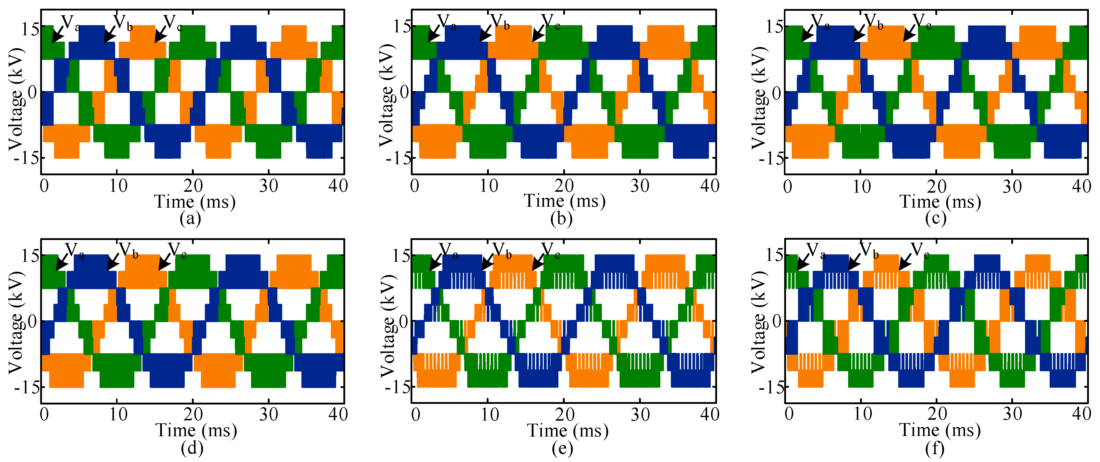
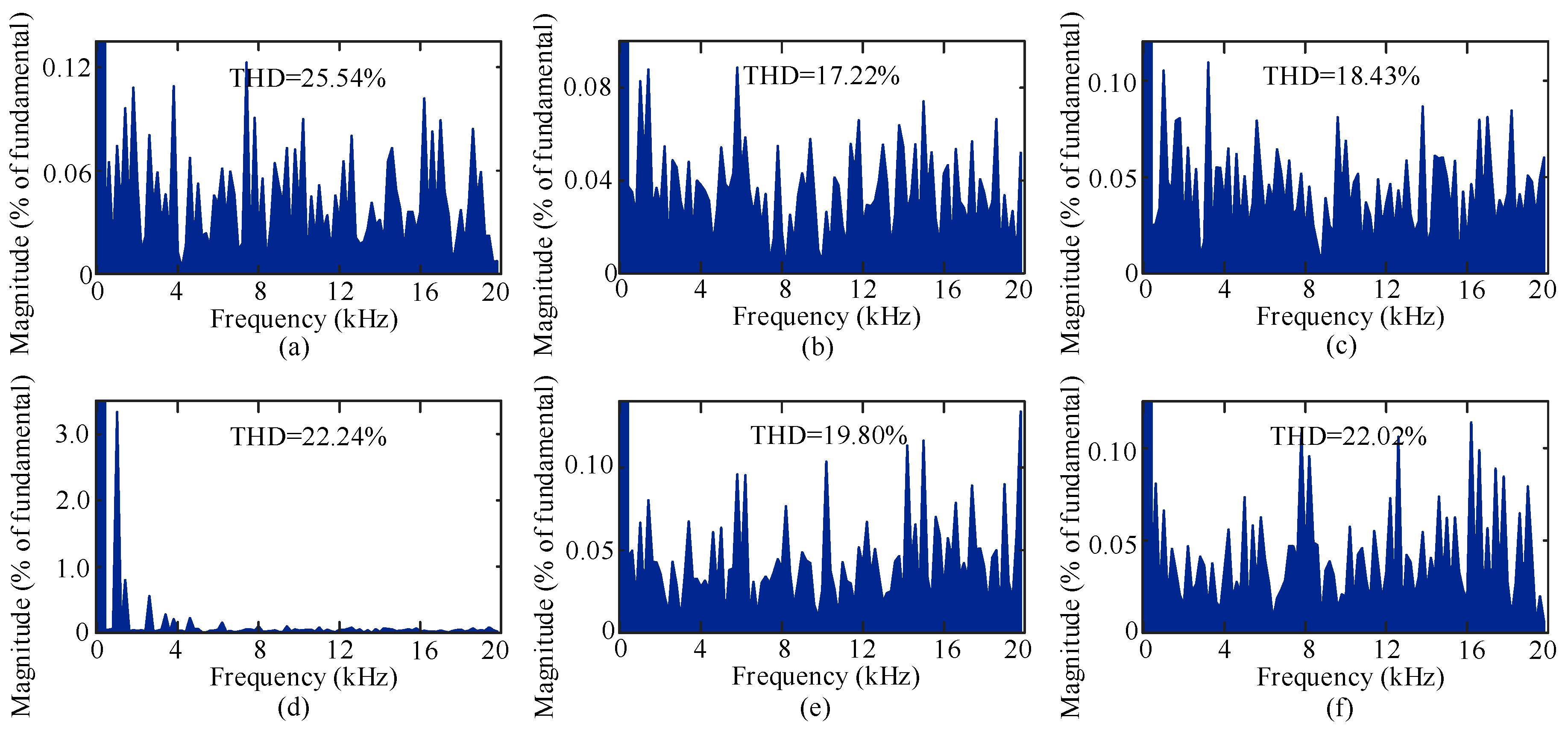
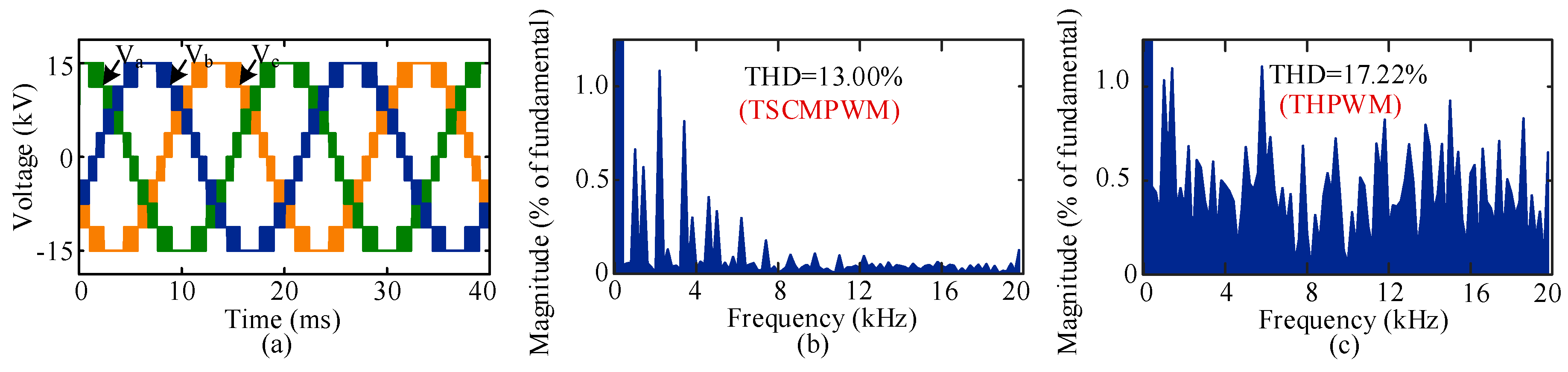
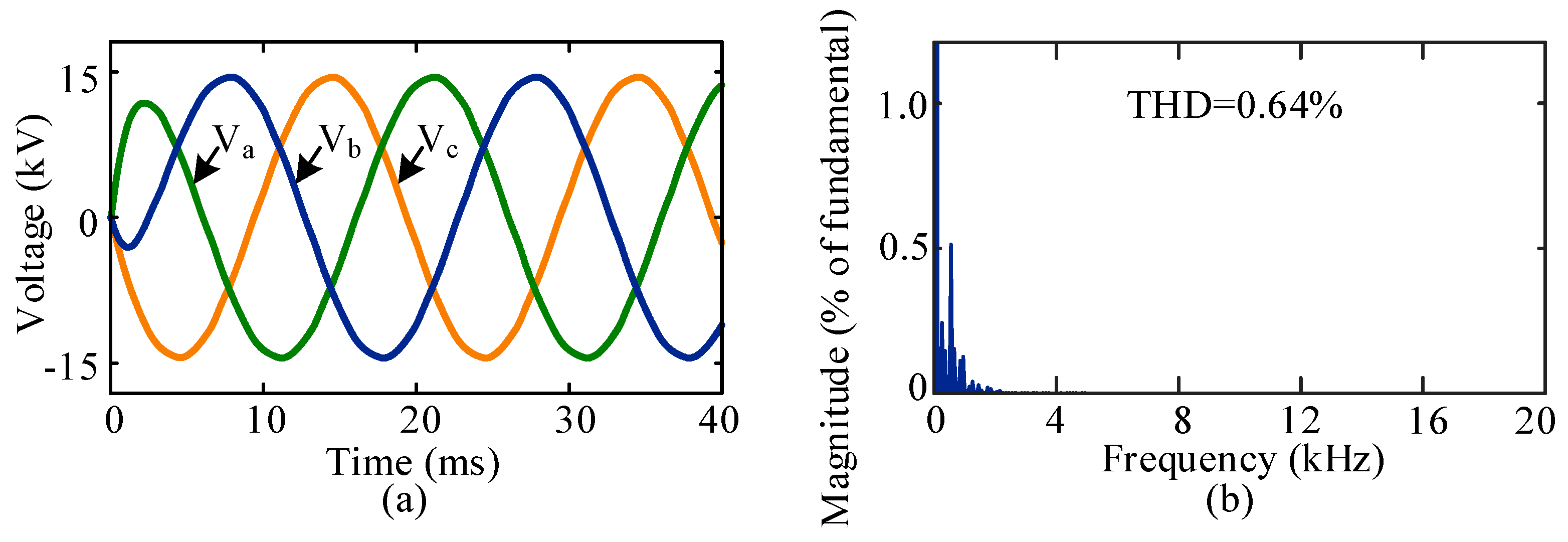
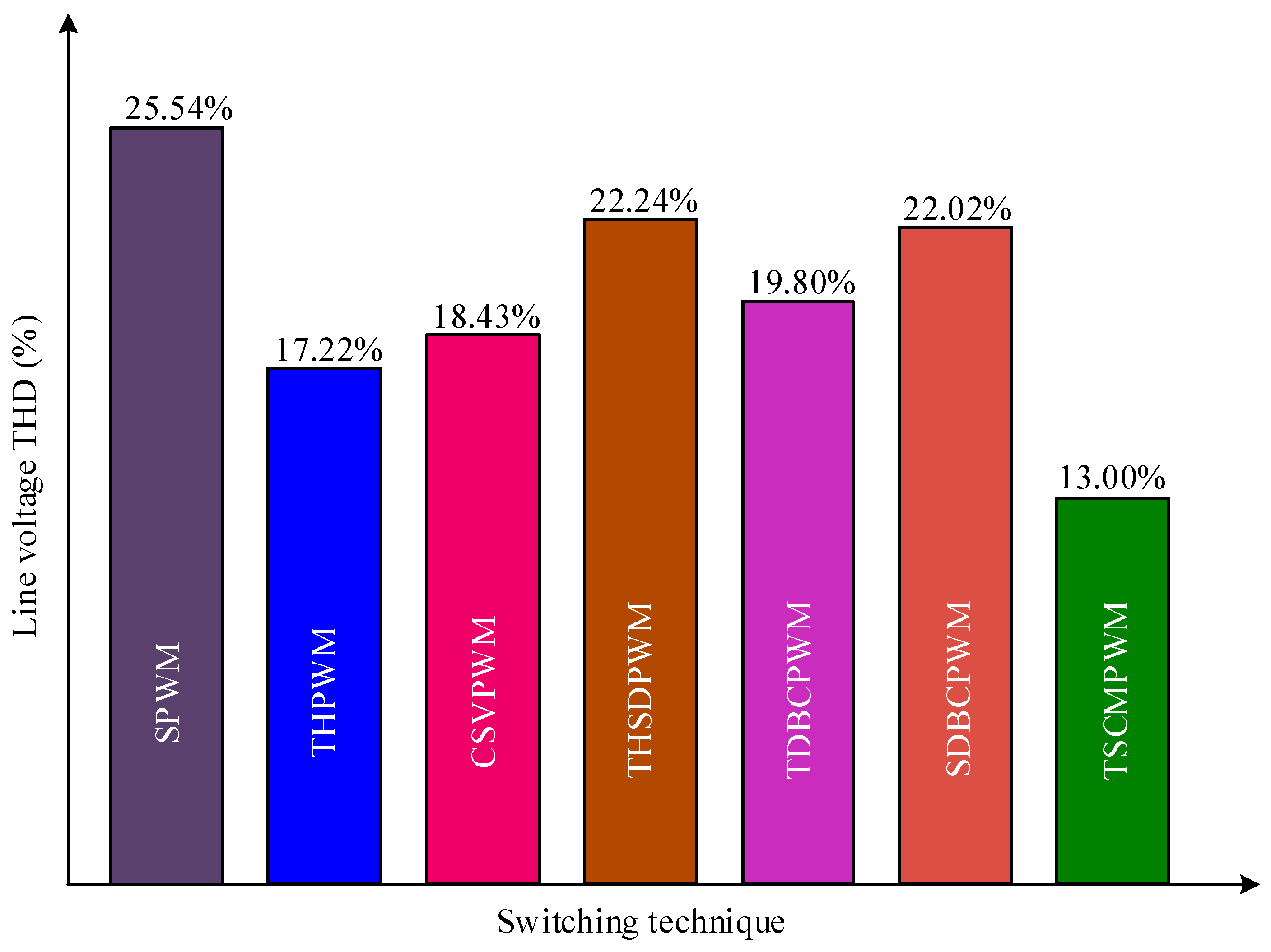
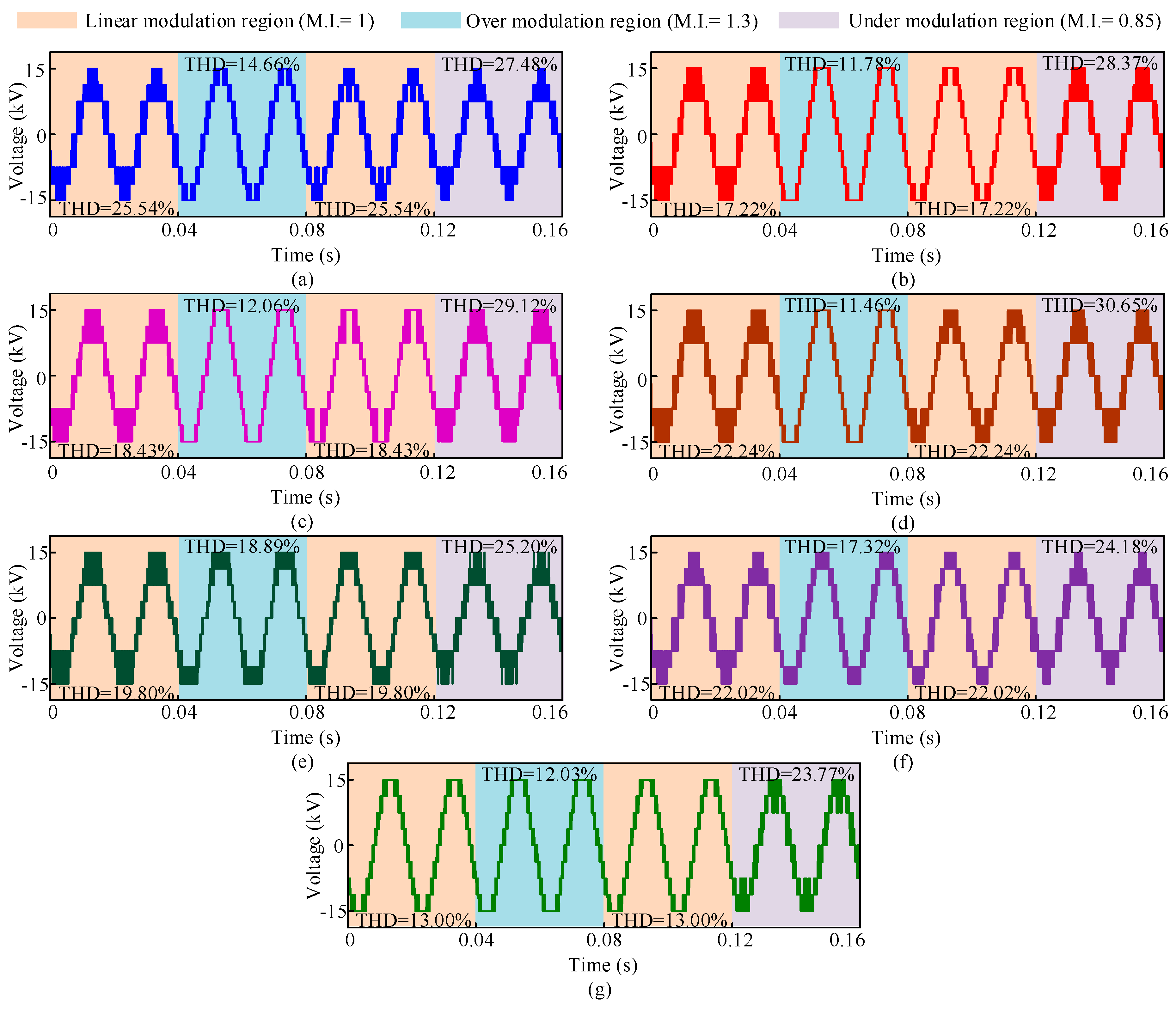
5.2. THD Profile of the MMC Inverter for Modulation Region Variation

Modulation index has significant impact on the THD of the inverter output voltage. Based on the grid conditions, controller varies the modulation index of the PWM technique employed in the inverter switching according to the requirement. There are three modulation regions of the PWM technique. These are under modulation region, linear modulation region, and over modulation region. Modulation region also affects the switching and conduction power losses of the inverter. As shown in Figure 13, detailed comparisons are made between the converter output line voltages with distinct modulation techniques in under, linear, and over modulation regions. It should be noted that the line voltage THD gets lower in over modulation region than that of linear and under modulation and the width of the gate pulses gets wider, which increases the conduction losses of the inverter. On the contrary, in under modulation region, lower order harmonics increase, which puts additional burden on the filtering circuitry. Therefore, for the desired output, the controller should return as soon as possible to the linear modulation mode. The proposed TSCMPWM offers 13.00%, 23.77%, and 12.03% THDs for linear, under, and over modulation regions, respectively. From Figure 13, it can be concluded that the proposed TSCMPWM technique shows better THD performance for three modulation regions compared to the existing SPWM, THPWM, CSVPWM, THSDPWM, TDBCPWM, and SDBCPWM techniques.

5.3. Dynamic Response of Inverter

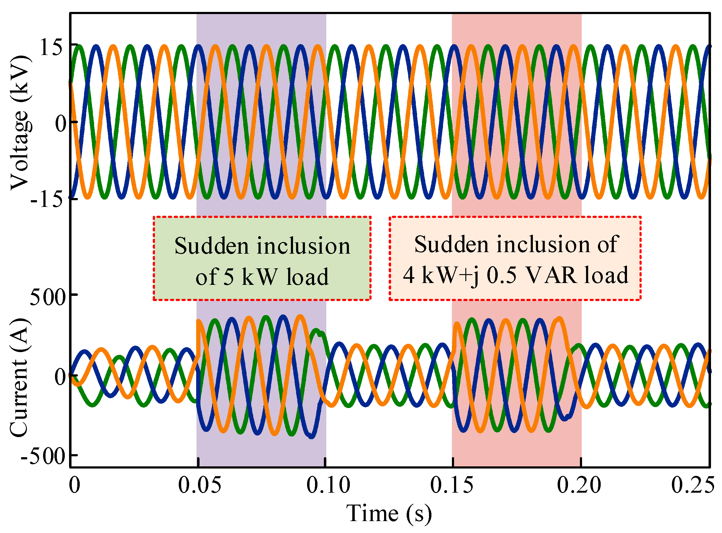
5.3.1. Sudden Load Change Response

Figure 14 depicts the dynamic load change response of the inverter voltage and current. Basically, the grid is connected to several local loads. At any instant of time, the total load on the inverter may change. So, it is mandatory to analyze the inverter current profile during load perturbations. At t = 0.05 s, 5 kW resistive type load is applied on the inverter suddenly and the load is withdrawn at t = 0.10 s. In this period, the inverter current has increased for the load changing effect, but it also shows the sinusoidal nature in the time of load changing period. Similarly, at t = 0.15 s, a 4 kW + j 0.5 VAR resistive-inductive type load is applied on the inverter and the load is withdrawn at t = 0.10 s. Same as before, the inverter current has increased during the load perturbation interval, which is also sinusoidal. Finally, from Figure 14, it can be concluded that the MMC inverter tied with medium voltage grid utilizing the proposed TSCMPWM technique shows satisfactory dynamic response during the load perturbation.

5.3.2. Voltage Sag/Swell Response

Figure 15a shows the inverter responses, such as the grid voltage sag and swell phenomenon, when there are variations in the grid. The voltage is sensed by the inverter when there is a voltage sag or swell on the grid side. The value of Vd (direct axis component of grid voltage) and Vq (quadrature axis component of grid voltage) are also modified due to the change in voltage amplitude, and the inverter modifies the modulation index accordingly. The inverter decreases its modulation index when voltage sags occur, and when voltage swells occur, the inverter raises its modulation index to cope with the grid voltage. Figure 15b depicts the zoomed inverter output phase voltage during sag and swell with the variation of the modulation index.

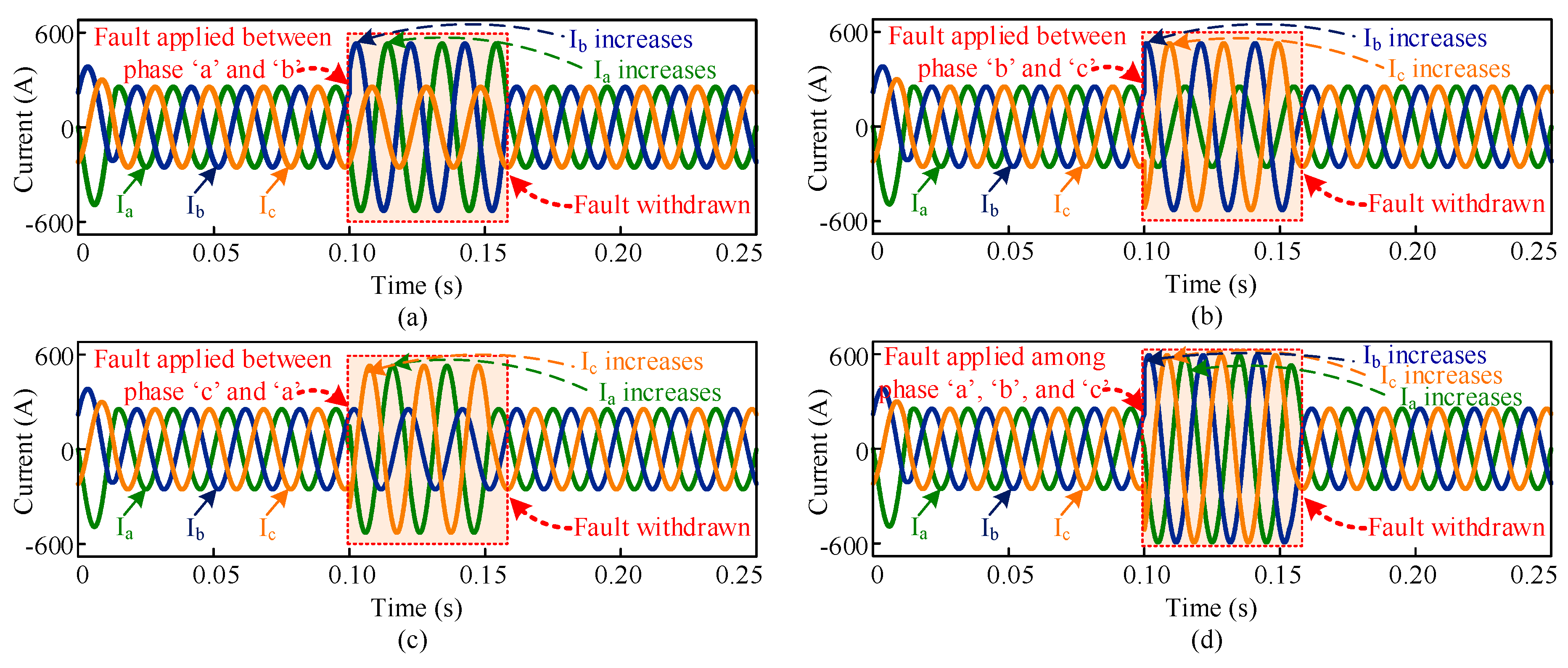
5.3.3. Response of Grid Current during Fault

The grid current is observed in this section under different fault conditions. Figure 16 describes the grid current profile under different fault conditions. The fault is applied in-between phases “a” and “b,” phases “b” and “c,” phases “a” and “c,” phases “a,” “b,” and “c” in Figure 16a–d, respectively. The amplitude of the current increases during fault period. After removing the fault, the current recovers its previous balanced condition very quickly, which demonstrates fast, robust, and dynamic characteristics of the system with the MMC inverter utilizing the proposed TSCMPWM technique for switching.

5.3.4. Comparative Analysis

In this section, the superiority of the proposed PWM technique with existing PWM techniques is investigated in terms of THD with the variation of modulation index and carrier frequency, inverter power loss, and THD variation with the change of inverter level. Table 3 shows the results of line voltage THDs by varying carrier frequency where modulation index is taken as 1. The proposed TSCMPWM offers low line voltage THD that of existing six PWM techniques.
Table 4 shows the results of line voltage THDs by varying modulation index where carrier frequency is taken as 2 kHz. For modulation index variation, the proposed TSCMPWM offers low line voltage THDs compared to existing six PWM techniques.
Figure 17 shows the inverter power losses for different PWM techniques with the variation of modulation index. Most of the practical system utilizes 0.7 to 1 modulation index variation. However, modulation index below 0.7 and over 1 have some detrimental effects on inverter performance. From Figure 17, it should be noted that the proposed TSCMPWM offers lower inverter power loss compared to existing six PWM techniques for a wide range of variation of modulation index.
Table 5 shows the results of line voltage THDs with the variation of inverter level. The proposed TSCMPWM technique offers 4.89% and 4.52% THD for 13 and 15 level MMC inverter, respectively, which complies IEEE 519-2014 standard. Compared to existing PWM techniques, the proposed TSCMPWM offers low line voltage THD for all inverter level as mentioned in Table 5.

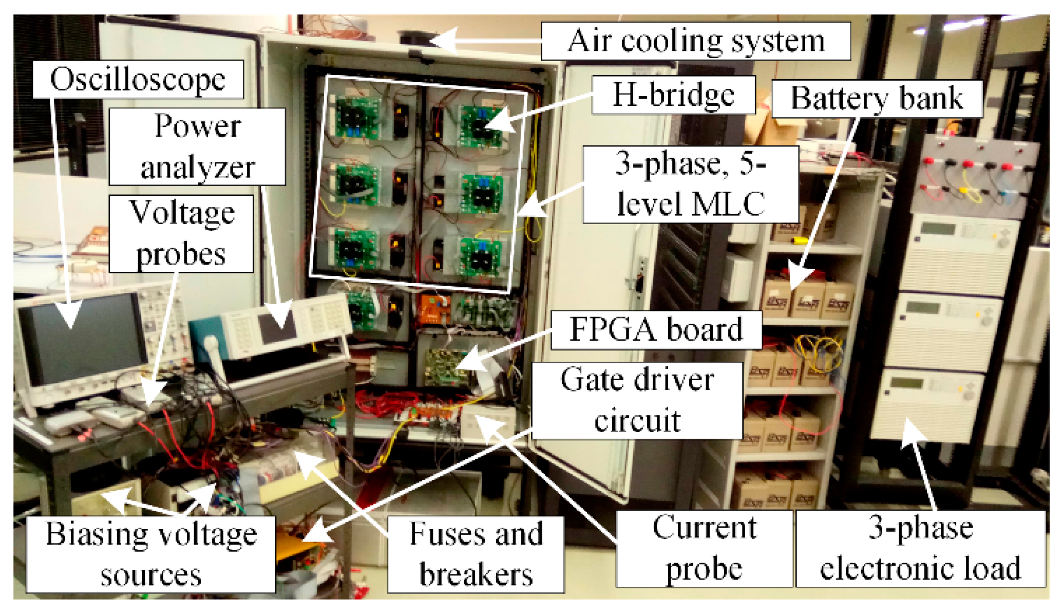
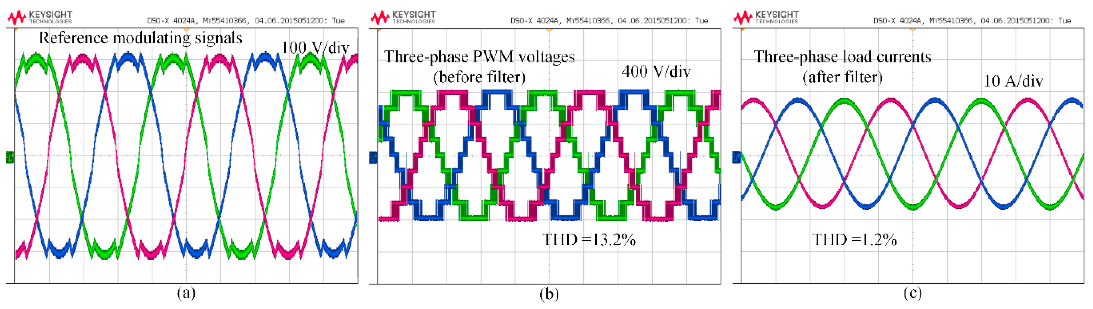
6. Experimental Validation

Figure 18 shows a down-scale laboratory setup of 5 kVA, 400 V, and 5-level MMC inverter. Necessary experiments are carried out on the MMC inverter to substantiate the improved performance of the proposed modulation technique. Three-phase electronic load module with a second-order LC filtering unit is connected at the output of the MMC inverter. To supply each H-bridge with 200 V dc, a battery bank is utilized, as shown in Figure 18. A Xilinx Spartan-3E FPGA is programmed to implement the proposed TSCMPWM scheme. Each H-bridge unit is made of compact SK30GH123 IGBT module from SEMIKRON, and all the switches are driven by a gate driver unit made of isolated gate driver SKHI 20opA.
Figure 19a shows the TSCMPWM reference modulating waveforms. The IGBT modules are operated with 1.2 kHz switching frequency. Figure 19b,c show the three-phase line–line PWM voltages before filter and three-phase line currents after filter, respectively. The voltage signals are collected with the KEYSIGHT N2791A voltage probes and the current signals are collected with the Agilent N2779A current probes. It can be observed from Figure 19b that the THD of the line–line voltages before filter under the proposed TSCMPWM is 13.2%, which is highly similar to the one found from simulations. Moreover, the line current THD is 1.2%, which is below the IEEE 519-2014 standard maximum THD limit (5%).
Figure 20 shows the load current performance under sudden load change conditions. First, a three-phase resistive load of 1.78 kW is connected in parallel, which causes high-current injection from the converter. The signals show steady and pollution free performance. Later, a load with pf of 0.9 (lagging) is connected in parallel. It can be observed from Figure 20 that the system offers distortion less signals even with the inclusion of the lagging load, however, the currents will be phase lagged.

7. Conclusions

In this paper, an advanced switching control technique for a 5 level grid-tied MMC inverter is proposed. The proposed technique offers 13% output line voltage THD (without line filter), which is lower than that of the existing most common PWM techniques. Moreover, the proposed technique ensures lower switching and conduction power losses of the inverter compared with the existing SPWM, THPWM, CSVPWM, THSDPWM, TDBCPWM, and SDBCPWM techniques. The proposed technique also provides better responses in terms of dynamic load change, fault, modulation index variation, and voltage sag/swell. Performance of the proposed modulation technique is evaluated in MATLAB/Simulink environment and tested with a reduced scale prototype test platform. Both simulation and experimental results show the effectiveness of the proposed modulation technique. The proposed PWM technique with the enlisted advantages could be a promising technology for the development of medium voltage power converters used in different emerging applications.

Author Contributions

Idea and conceptualization, S.H., S.P.B. and M.R.I.; design and simulation, S.H., S.P.B. and M.K.H.; prototyping, M.A.R., M.R.I. and S.P.B.; writing and drawing, S.H., S.P.B., S.J., M.A.R. and M.R.I.; revision and correction, M.R.I. and M.K.H. All authors have read and agreed to the published version of the manuscript.

Funding

This research received no external funding.

Institutional Review Board Statement

Not applicable.

Informed Consent Statement

Not applicable.

Data Availability Statement

Not applicable.

Conflicts of Interest

The authors declare no conflict of interest.

References

  1. Azmi, S.A.; Adam, G.P.; Ahmed, K.H.; Finney, S.J.; Williams, B.W. Grid interfacing of multimegawatt photovoltaic inverters. IEEE Trans. Power Electron. 2013, 28, 2770–2784. [Google Scholar] [CrossRef]
  2. Kroposki, B.; Johnson, B.; Zhang, Y.; Gevorgian, V.; Denholm, P.; Hodge, B.; Hannegan, B. Achieving a 100% renewable grid: Operating electric power systems with extremely high levels of variable renewable energy. IEEE Power Energy Mag. 2017, 15, 61–73. [Google Scholar] [CrossRef]
  3. Mondol, M.H.; Tür, M.R.; Biswas, S.P.; Hosain, M.K.; Shuvo, S.; Hossain, E. Compact three phase multilevel inverter for low and medium power photovoltaic systems. IEEE Access 2020, 8, 60824–60837. [Google Scholar] [CrossRef]
  4. Chowdhury, M.R.; Rahman, M.A.; Islam, M.R.; Mahfuz-Ur-Rahman, A.M. A New Modulation Technique to Improve the Power Loss Division Performance of the Multilevel Inverters. IEEE Trans. Ind. Electron. 2020. [Google Scholar] [CrossRef]
  5. Islam, M.R.; Mahfuz-Ur-Rahman, A.M.; Muttaqi, K.M.; Sutanto, D. State-of-the-art of the medium-voltage power converter technologies for grid integration of solar photovoltaic power plants. IEEE Trans. Energy Convers. 2019, 34, 372–384. [Google Scholar] [CrossRef]
  6. Perez, M.A.; Bernet, S.; Rodriguez, J.; Kouro, S.; Lizana, R. Circuit topologies, modeling, control schemes, and applications of modular multilevel converters. IEEE Trans. Power Electron. 2015, 30, 4–17. [Google Scholar] [CrossRef]
  7. McGrath, B.P.; Holmes, D.G.; Kong, W.Y. A decentralized controller architecture for a cascaded H-bridge multilevel converter. IEEE Trans. Ind. Electron. 2014, 61, 1169–1178. [Google Scholar] [CrossRef]
  8. Babaei, E.; Laali, S.; Alilu, S. Cascaded multilevel inverter with series connection of novel H-bridge basic units. IEEE Trans. Ind. Electron. 2014, 61, 6664–6671. [Google Scholar] [CrossRef]
  9. Buccella, C.; Cecati, C.; Cimoroni, M.G.; Razi, K. Analytical method for pattern generation in five-level cascaded H-bridge inverter using selective harmonic elimination. IEEE Trans. Ind. Electron. 2014, 61, 5811–5819. [Google Scholar] [CrossRef]
  10. Chattopadhyay, S.K.; Chakraborty, C. A new multilevel inverter topology with self-balancing level doubling network. IEEE Trans. Ind. Electron. 2014, 61, 4622–4631. [Google Scholar] [CrossRef]
  11. Soto-Sanchez, D.E.; Pena, R.; Cardenas, R.; Clare, J.; Wheeler, P. A cascade multilevel frequency changing converter for high-power applications. IEEE Trans. Ind. Electron. 2013, 60, 2118–2130. [Google Scholar] [CrossRef]
  12. Okazaki, Y.; Kawamura, W.; Hagiwara, M.; Akagi, H.; Ishida, T.; Tsukakoshi, M.; Nakamura, R. Experimental comparisons between modular multilevel DSCC inverters and TSBC converters for medium-voltage motor drives. IEEE Trans. Power Electron. 2017, 32, 1805–1817. [Google Scholar] [CrossRef]
  13. Kumar, Y.S.; Poddar, G. Control of medium-voltage ac motor drive for wide speed range using modular multilevel converter. IEEE Trans. Ind. Electron. 2017, 64, 2742–2749. [Google Scholar] [CrossRef]
  14. Sadigh, A.K.; Dargahi, V.; Corzine, K.A. Analytical determination of conduction and switching power losses in flying-capacitor-based active neutral-point-clamped multilevel converter. IEEE Trans. Power Electron. 2016, 31, 5473–5494. [Google Scholar] [CrossRef]
  15. Tian, H.; Li, Y.W. Carrier-based stair edge PWM (SEPWM) for capacitor balancing in multilevel converters with floating capacitors. IEEE Trans. Ind. Appl. 2018, 54, 3440–3452. [Google Scholar] [CrossRef]
  16. Sanchez-Ruiz, A.; Mazuela, M.; Alvarez, S.; Abad, G.; Baraia, I. Mediumvoltage–high power converter topologies comparison procedure, for a 6.6 kV drive application using 4.5 kV IGBT modules. IEEE Trans. Ind. Electron. 2012, 59, 1462–1476. [Google Scholar] [CrossRef]
  17. Haq, S.; Biswas, S.P.; Hosain, M.K.; Sheikh, M.R.I. Performance analysis of switching techniques in modular multilevel converter fed induction motor. In Proceedings of the 2019 4th International Conference on Electrical Information and Communication Technology (EICT), Khulna, Bangladesh, 20–22 December 2019; pp. 1–6. [Google Scholar] [CrossRef]
  18. Islam, M.M.; Rahman, M.A.; Islam, M.R. Power loss and thermal impedance modeling of multilevel power converter with discontinuous modulation. IEEE Trans. Energy Convers. 2020. [Google Scholar] [CrossRef]
  19. Mandol, M.H.; Biswas, S.P.; Roy, T.K.; Hosain, M.K.; Kibria, M.F. A novel modulation scheme to improve the injected power quality for modular multilevel medium voltage grid-tied power converters. In Proceedings of the 2019 International Conference on Electrical, Computer and Communication Engineering (ECCE), Cox’s Bazar, Bangladesh, 7–9 February 2019; pp. 1–6. [Google Scholar] [CrossRef]
  20. Chavarria, J.; Biel, D.; Guinjoan, F.; Meza, C.; Negroni, J.J. Energybalance control of PV cascaded multilevel grid-connected inverters under level-shifted and phase-shifted PWMs. IEEE Trans. Ind. Electron. 2013, 60, 98–111. [Google Scholar] [CrossRef]
  21. Zhao, D.; Hari, V.S.S.P.K.; Narayanan, G.; Ayyanar, R. Spacevector-based hybrid pulse width modulation techniques for reduced harmonic distortion and switching loss. IEEE Trans. Power Electron. 2010, 25, 760–774. [Google Scholar] [CrossRef]
  22. Mondol, M.H.; Biswas, S.P.; Roy, T.K. A new multilevel inverter with alleviated number of switches for renewable energy applications. In Proceedings of the 2020 IEEE Region 10 Symposium (TENSYMP), Dhaka, Bangladesh, 5–7 June 2020; pp. 961–964. [Google Scholar] [CrossRef]
  23. Biswas, S.P.; Anower, M.S.; Sheikh, M.R.I.; Islam, M.R.; Kouzani, A.Z.; Mahmud, M.A.P. A new modulation technique to improve the performance of three phase inverters. In Proceedings of the 2020 IEEE International Conference on Applied Superconductivity and Electromagnetic Devices (ASEMD), Tianjin, China, 16–18 October 2020; pp. 1–2. [Google Scholar] [CrossRef]
  24. Haq, S.; Biswas, S.P.; Jahan, S.; Islam, M.R.; Mahmud, M.A.P.; Kouzani, A.Z. An advanced modulation technique to improve the performance of modular multilevel converter. In Proceedings of the 2020 IEEE International Conference on Applied Superconductivity and Electromagnetic Devices (ASEMD), Tianjin, China, 16–18 October 2020; pp. 1–2. [Google Scholar] [CrossRef]
Figure 1. The modular multilevel cascaded (MMC) inverter-based grid-tied photovoltaic (PV) system.
Energies 14 00331 g001
Figure 2. Modulating signals with the modulation techniques: (a) sine pulse width modulation (SPWM), (b) third harmonic-injected PWM (THPWM), (c) conventional space vector PWM (CSVPWM), (d) third harmonic sixty-degree PWM (THSDPWM), (e) thirty-degree bus clamping PWM (TDBCPWM) and (f) sixty-degree bus clamping PWM (SDBCPWM).
Energies 14 00331 g002
Figure 3. Inverter line voltage with modulation techniques: (a) SPWM, (b) THPWM, (c) CSVPWM, (d) THSDPWM, (e) TDBCPWM, and (f) SDBCPWM.
Energies 14 00331 g003
Figure 4. Inverter line voltage total harmonic distortions (THDs) with the modulation techniques: (a) SPWM, (b) THPWM, (c) CSVPWM, (d) THSDPWM, (e) TDBCPWM, and (f) SDBCPWM.
Energies 14 00331 g004
Figure 5. Proposed triangle saturated common mode pulse width modulation (TSCMPWM) modulating signal.
Energies 14 00331 g005
Figure 6. Proposed TSCMPWM modulating signal generation technique: (a) step by step procedure and (b) flowchart/algorithm.
Energies 14 00331 g006
Figure 7. Illustration of gate pulse generation scheme using proposed TSCMPWM technique for 5-level MMC inverter (only modulating signal, Sa is shown here to demonstrate the system for better view).
Energies 14 00331 g007
Figure 8. (a) Output line voltage with TSCMPWM scheme, (b) frequency spectra of line voltage with TSCMPWM scheme, and (c) frequency spectra of line voltage with THPWM scheme.
Energies 14 00331 g008
Figure 9. With the proposed TSCMPWM: (a) filtered line voltages and (b) frequency spectra.
Energies 14 00331 g009
Figure 10. Comparisons of the MMC inverter line voltage THDs for the existing and the proposed TSCMPWM techniques.
Energies 14 00331 g010
Figure 11. Control scheme for the MMC inverter-based grid-tied PV system with the implementation of the proposed TSCMPWM technique.
Energies 14 00331 g011
Figure 12. Power loss analysis against modulation index variation for the proposed TSCMPWM technique.
Energies 14 00331 g012
Figure 13. Converter output voltage profiles with the variation of modulation region for different PWM schemes: (a) SPWM, (b) THPWM, (c) CSVPWM, (d) THSDPWM, (e) TDBCPWM, (f) SDBCPWM, and (g) proposed TSCMPWM.
Energies 14 00331 g013
Figure 14. Sudden load change response of the inverter.
Energies 14 00331 g014
Figure 15. Voltage sag/swell response: (a) grid line voltage and (b) zoomed inverter phase voltage.
Energies 14 00331 g015
Figure 16. Fault response in inverter current: (a) fault is applied in phase “a” and “b” (b) fault is applied in phase “b” and “c” (c) fault is applied in phase “c” and “a,” and (d) fault is applied in phase “a,” “b,” and “c.”
Energies 14 00331 g016
Figure 17. Inverter power loss for different PWM techniques with the variation of modulation index at 2 kHz carrier frequency.
Energies 14 00331 g017
Figure 18. Photograph of the experimental setup.
Energies 14 00331 g018
Figure 19. At steady-state condition: (a) proposed TSCMPWM modulating signals, (b) three-phase line–line PWM voltages before filter, and (c) three-phase load currents after filter.
Energies 14 00331 g019
Figure 20. Three-phase load currents under sudden load change.
Energies 14 00331 g020
Table 1. Mathematical expression of existing switching technique.
Switching TechniquesMathematical Expressions
SPWM S 1 = A   sin ( ω t + θ )
[ S 1 a S 1 b S 1 c ] = [ S 1 θ = 0 ° S 1 θ = 120 ° S 1 θ = 120 ° ]
THPWM B = k A   sin ( 3 ω t )
S 2 = A sin ( ω t + θ ) + B
[ S 2 a S 2 b S 2 c ] = [ S 2 θ = 0 ° S 2 θ = 120 ° S 2 θ = 120 ° ]
CSVPWM S 3 = 2 3   [ A   sin ( ω t + θ ) ] 1 2 { max ( S 1 a ,   S 1 b , S 1 c ) } + 1 2 { min ( S 1 a ,   S 1 b , S 1 c ) }
[ S 3 a S 3 b S 3 c ] = [ S 3 θ = 0 ° S 3 θ = 120 ° S 3 θ = 120 ° ]
THSDPWM X 1 = S 1
= 0.76 A   ( w h e n   S 1 > 0.76 A )
= 0.76 A   ( w h e n   S 1 < 0.76 A )
S 4 = X 1 = B
[ S 4 a S 4 b S 4 c ] = [ S 4 θ = 0 ° S 4 θ = 120 ° S 4 θ = 120 ° ]
TDBCPWM S 5 = A sin ( ω t + θ ) + f 1 ( α ) { V c max ( S 1 a ,   S 1 b , S 1 c ) } + f 2 ( α ) { V c min ( S 1 a ,   S 1 b , S 1 c ) }
Where, f 1 ( α ) = 0   ( w h e n   0 ° < α < 60 ° )
= 1   ( w h e n   60 ° < α < 120 ° )
f 2 ( α ) = 1   ( w h e n   0 ° < α < 60 ° )
= 0   ( w h e n   60 ° < α < 120 ° )
[ S 5 a S 5 b S 5 c ] = [ S 5 θ = 0 ° S 5 θ = 120 ° S 5 θ = 120 ° ]
SDBCPWM S 6 = A sin ( ω t + θ ) + f 2 ( α ) { V c max ( S 1 a ,   S 1 b , S 1 c ) } + f 1 ( α ) { V c min ( S 1 a ,   S 1 b , S 1 c ) }
[ S 6 a S 6 b S 6 c ] = [ S 6 θ = 0 ° S 6 θ = 120 ° S 6 θ = 120 ° ]
Table 2. Inverter line voltage total harmonic distortions (THDs) for different existing switching techniques.
PWM TechniquesSPWMTHPWMCSVPWMTHSDPWMTDBCPWMSDBCPWM
THD (%)25.5417.2218.4322.2419.8022.02
Table 3. Line voltage THDs of different pulse width modulation (PWM) techniques for carrier frequency variation.
Line Voltage THDs (%) for Different Carrier Frequencies (C. F.) with Modulation Index = 1
PWM TechniqueC.F. = 1 kHzC.F. = 2 kHzC.F. = 3 kHzC.F. = 4 kHz
SPWM25.4925.5425.5725.48
THPWM17.2017.2217.1917.24
CSVPWM18.3718.4318.3318.46
THSDPWM25.4922.2425.5725.48
TDBCPWM19.7619.8019.7519.84
SDBCPWM21.9122.0221.9121.98
TSCMPWM13.0613.0013.1113.07
Table 4. Line voltage THDs of different PWM techniques for modulation index variation.
Line Voltage THDs (%) for Different Modulation Indexes (M.I.) with Carrier Frequency = 2 kHz
PWM TechniqueM.I. = 0.7M.I. = 0.8M.I. = 0.9M.I. = 1.0
SPWM28.0429.7228.7125.54
THPWM36.2833.0426.5517.22
CSVPWM37.1334.1527.9918.43
THSDPWM37.1435.0529.8322.24
TDBCPWM32.6529.7925.6419.80
SDBCPWM25.2326.5225.6922.02
TSCMPWM24.5019.5414.4813.00
Table 5. Line voltage THDs of different PWM techniques for inverter level variation.
Line Voltage THDs (%)
PWM Technique5 Level7 Level9 Level11 Level13 Level15 Level
SPWM25.5414.9412.288.637.715.95
THPWM17.2211.899.487.406.145.47
CSVPWM18.4313.3610.558.757.356.28
THSDPWM22.2416.8112.519.878.547.33
TDBCPWM19.8011.659.538.366.385.18
SDBCPWM22.0211.4710.117.836.905.07
TSCMPWM13.009.4638.035.904.894.52
Publisher’s Note: MDPI stays neutral with regard to jurisdictional claims in published maps and institutional affiliations.

