Article

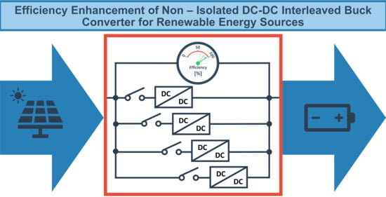
Efficiency Enhancement of Non-Isolated DC-DC Interleaved Buck Converter for Renewable Energy Sources

Department of Theoretical and Industrial Electrical Engineering, Technical University of Košice, 04200 Košice, Slovakia
*
Author to whom correspondence should be addressed.
Energies 2021, 14(14), 4127; https://doi.org/10.3390/en14144127
Submission received: 16 June 2021 / Revised: 5 July 2021 / Accepted: 6 July 2021 / Published: 8 July 2021
(This article belongs to the Special Issue DC-DC Converters Technologies, Applications and Optimization)

Abstract

:
The article describes the principles based on which it is possible to obtain energy from renewable sources more efficiently. The principles use the conventional DC-DC interleaved buck converter based on the common electronic component types and the control strategy. A novelty of such a proposed solution lies in the methods which are not new, but with the right combination, better results can be achieved. The resulting method can be implemented into various topologies where the highest efficiency for wide input power is required. In case of the renewable energy sources where the power can vary hugely during the day, the proposed method can be implemented. Therefore, the article provides several steps, from calculation through simulation to experimental results that brings reader close to understanding of a such proposed solution.

Graphical Abstract

1. Introduction

DC-DC converters play a very important role in drawing energy from the renewable energy sources. The main reason is that the renewable energy sources do not produce constant power during the day. Therefore, they cannot be connected to the constant load, or to the load directly. This main drawback has a solution in implementing the DC-DC converter which, with an appropriate control strategy, can change the load factor to draw maximum energy as possible, or create a desired voltage level for connected load [1].
Currently, there are many solutions for how to create a more effective control strategy, to find the maximum power point more accurately, and much quicker [2]. In this case, the article will be describing the power-related aspect of the interleaved DC-DC converters and a solution which can be used to enhance their efficiency.
Interleaved DC-DC converters provide several advantages against non-interleaved versions. For instance, the interleaved converter produces lower current ripple [3] for the same switching frequency, working in a narrower area of discontinuous current, and providing a higher efficiency of power conversion.
To achieve smaller size of input and output filters, and lighter weights of the converters, it is necessary to operate converters at the highest possible switching frequency. However, high-switching devices for high power are expensive compared to low-switching devices with low power. Therefore, using several DC-DC converters working in an interleaved mode creates a high-frequency output with current sharing between each individual leg. Therefore, the soft switching technique can be omitted due to its low switching frequency in each individual converter’s leg, and the expensive switching components can be replaced for inexpensive versions.
Interleaved DC-DC converters in various converter topologies can be found in many applications. In some cases, the interleaved mode can be implemented in novel topologies, or basic topologies with novel electrical components [4,5], and many other applications. For example, to enhance the output voltage ratio of boost converters [6,7,8], or for use in bidirectional connection [9,10], or for achieving better efficiency on passive components [11]. The interleaved connection finds its way in renewable energy sources [12,13,14], electrical vehicles [15], in isolated power sources [16,17], and many others. In all mentioned cases of DC-DC converters, the proposed solution can enhance their efficiency.
All of them use interleaved, multiphase or multi-leg connection, but none of the abovementioned explain why the specific converter leg number is used. Therefore, it is difficult to find similar comparable results in the literature. For instance, the references [18,19] describe the impact of number of phases in interleaved converters in different way that can be used for achieving more efficiency. Due to the of lack contribution numbers in the interleaved converter effective leg number field, the article in addition provides a simple solution to achieve better efficiency, which will be described later.
Due to the huge number of advantages in using interleaved DC-DC converters, their application for renewable energy sources is widely used. However, the number of converter legs that should be used with specific electrical components in specific range of input power is still an open question. If the control algorithm allows a converter leg number change, then, with the right implementation, it also could contribute to the enhancement of converter efficiency. The solution provided in this paper can be used to determine converters optimum leg number based on used electrical components, and input power to achieve better efficiency.
Therefore, the optimal number of legs in the interleaved buck converter with specific electrical components remains an open question. To answer that question, an analysis should be made from the perspective of achieving maximum efficiency. For that reason, the paper is further structured in the following way:
In the beginning, the paper describes the calculations used to obtain the final mathematical form. With such a mathematical form, the right interleaved converter legs number can be determined. Based on the expressed mathematical form, the control unit can select the optimum interleaved converter legs number to achieve better efficiency in various input power.
At the end of the paper, the simulation and experimental results on a four-leg DC-DC interleaved converter validate the proposed final mathematical form.

2. Interleaved DC-DC Converter Analysis

The schematic connection of the interleaved converter with n legs number is shown in Figure 1. The figure shows the basic scheme (see Figure 1a) and the scheme with parasitic electrical components of the converter (see Figure 1b). As the converter topology is a cascaded DC-DC Buck-Boost converter in this case, only work carried out in buck mode where the second transistor is omitted is considered [20]. However, the diodes D12 to Dn2 should be included for efficiency determination. Boost mode analysis is out of scope of this article. As will be described later, the calculation can be easily modified to achieve final mathematical form for any topology the application required. Because the simulations and the experimental results consist of the mentioned diodes, the analysis will also consider these diodes. The presence of the diodes does not invalidate following proposed analysis, the simulation or the validity of the experimental results.
All electrical components which contain index P represent the parasitic components of a real model of the converter. For electrical current, the first Kirchhoff law is applied (1).
i = j = 1 n i j
Each converter leg works with the same switching frequency and duty cycle as the other converter legs. The control signals are time shifted based on T/n, where T is switching period and the n is a quantity of converter legs. With such phase-shifted control signals, the interleaved mode will be achieved for every leg number change.

2.1. The First Time Period Analysis–Energy Accumulation

In this working period, the switching device in this case a MOSFET transistor is closed, which will cause the energy accumulation in the main induction element of the circuit. The described situation can be seen in Figure 2.
To the n conductive converter leg, the second Kirchhoff law can be applied (2).
V + R P n 1 i n + L P n 1 d i n d t + r D S ( o n ) n i n +   R L n i n + L n d i n d t + V F + R P n 2 i n +   L P n 2 d i n d t + V Z = 0
where V is an input voltage, RPn1 and LPn1 is a parasitic resistance and a parasitic inductance, respectively, of the input wire. rDS(on) is a MOSFET transistor resistance when it is turned on, RLn and Ln is a resistance and inductance of the main inductor, respectively. VF is a voltage drop on a diode, RPn2 is an output wire resistance leaded to load and the VZ is a voltage load.
Due of resistive and inductive load, the current waveform in continuous conduction mode (CCM) will have a shape according to Figure 3.
According to Figure 2, the loop circuit can be simplified by the parameter’s concentration (3)–(6).
V Z = Z I = Z i = 1 n i i Z n i n
V F = V T O + r F i n
R n 1 = R P n 1 + r D S ( o n ) + R L n + R P n 2 + r F
L n 1 = L P n 1 + L n + L P n 2
where VTO is a threshold voltage of the diode, Rn1 is a n-th leg resistance of the first time period, rF is a diode resistance in the forward direction and Ln1 is an induction of n-th leg converter in the first time period.
Based on (3) to (6), the (2) can be modified as follows (7):
V T O V + Z n i n + R n 1 i n + L n 1 d i n d t = 0
Rewriting (7) with shape operator, the equation will obtain the following format:
V T O V + Z n i ^ n + R n 1 i ^ n + p L n 1 i ^ n p L n 1 I 1 = 0
Now, from (8) the current can be expressed as follows:
i ^ n = V V T O ( R n 1 + n Z ) ( R n 1 + n Z ) L n 1 ( R n 1 + n Z ) L n 1 + p + I 1 p ( R n 1 + n Z ) L n 1 + p
By completing a back transformation of (9) to the time domain, we obtain (10).
i n = V V T O ( R n 1 + n Z ) ( 1 e ( R n 1 + n Z ) L n 1 t ) + I 1 e ( R n 1 + n Z ) L n 1 t
If, in this time domain, the expression of the current we substitute t = ton = D/f, then at a given moment in time, it obtains a current I2, according to Figure 3. The resulting equation for the current I2 takes a following form:
I 2 = V V T O ( R n 1 + n Z ) ( 1 e ( R n 1 + n Z ) L n 1 D f ) + I 1 e ( R n 1 + n Z ) L n 1 D f
where D is a duty cycle, and f is a switching frequency.
To obtain the current value I1, the second time period of the converter will be described.

2.2. The Second Time Period Analysis—Energy Transferred to the Load

In the second working period of the converter, the switching device will turn off and an accumulated energy in the main inductor will be transferred to the load through diodes Dn1 and Dn2, as seen in Figure 4.
For the n conductive converter leg, the second Kirchhoff law can be applied as follows (12).
V Z + V F + R L n i n + L n d i n d t +   V F + R P n 2 i n + L P n 2 d i n d t = 0
where (3) can be applied as well as the following equations to simplified loop circuit by parameter concentration:
R n 2 = R L n + 2 r F + R P n 2
L n 2 = L n + L P n 2
Applying equations for parameter concentration, the modified (12) will get the following form:
n Z i n + 2 V T O + R n 2 i n + L n 2 d i n d t = 0
Rewriting (15) with shape operator, the equation will obtain the following format:
n Z i ^ n + 2 V T O + R n 2 i ^ n + p L n 2 i ^ n p L n 2 I 2 = 0
Now, from (16), the current can be expressed as follows:
i ^ n = 2 U T O ( R n 2 + n Z ) ( R n 2 + n Z ) L n 2 ( R n 2 + n Z ) L n 2 + p + I 2 p ( R n 2 + n Z ) L n 2 + p
By completing a back transformation of (17) to the time domain, we obtain (18).
i n = 2 V T O ( R n 2 + n Z ) ( 1 e ( R n 2 + n Z ) L n 2 t ) + I 2 e ( R n 2 + n Z ) L n 2 t
If in this time domain expression of the current we substitute t = toff = (1 − D)/f, then at a given moment in time, it obtains a current I1, according to Figure 3. The resulting equation for the current I1 takes a following form:
I 1 = 2 V T O ( R n 2 + n Z ) ( 1 e ( R n 2 + n Z ) L n 2 ( 1 D ) f ) + I 2 e ( R n 2 + n Z ) L n 2 ( 1 D ) f

2.3. Total Power Loss Calculation

Based on (11) and (19), it is possible to obtain current values of the I1 and the I2 at the beginning of each time period.
Next, the current value of I2 from (11) is substituted into (19), which results in:
I 1 = 2 V T O ( R n 2 + n Z ) ( 1 e ( R n 2 + n Z ) L n 2 ( 1 D ) f ) +   ( V V T O R n 1 + n Z ( 1 e ( R n 1 + n Z ) L n 1 D f ) + I 1 e ( R n 1 + n Z ) L n 1 D f ) e ( R n 2 + n Z ) L n 2 ( 1 D ) f
The final expression of the I1 current value is obtained after adjusting (20) to the form:
I 1 = 2 V T O ( R n 2 + n Z ) ( 1 e ( R n 2 + n Z ) L n 2 ( 1 D ) f ) + ( ( V V T O ) ( R n 1 + n Z ) ( 1 e ( R n 1 + n Z ) L n 1 D f ) e ( R n 2 + n Z ) L n 2 ( 1 D ) f ) ( 1 e ( R n 1 + n Z ) L n 1 D f e ( R n 2 + n Z ) L n 2 ( 1 D ) f )
The current value expression of I2 can be achieved by substitution of (21) into (11), which results in:
I 2 = V V T O ( R n 1 + n Z ) ( 1 e ( R n 1 + n Z ) L n 1 z f ) +   ( 2 V T O ( R n 2 + n Z ) ( 1 e ( R n 2 + n Z ) L n 2 ( 1 D ) f ) + ( V V T O ( R n 1 + n Z ) ( 1 e ( R n 1 + n Z ) L n 1 D f ) e ( R n 2 + n Z ) L n 2 ( 1 D ) f ) ( 1 e ( R n 1 + n Z ) L n 1 D f e ( R n 2 + n Z ) L n 2 ( 1 D ) f ) ) e ( R n 1 + n Z ) L n 1 D f
Based on (10), (18), (21) and (22), the current waveform can be determined for any leg of the converter.
To determine the optimum legs number of the converter, the power losses based on leg number were determined. The power losses occur in conduction losses with static (quiescent) losses for both, time periods as well as for switching losses of the power converter. The considered losses in a power converter are the losses produced by the semiconductor switches (MOSFETs and diodes) and the passive components (inductors). Their losses can be expressed as follows:
Conduction losses:
-PRPn1—Power losses due to current flowing through input wire resistance of the converter n leg;
-PMF—Power losses in the MOSFET transistor in conductive state;
-PMR—Power losses in the MOSFET in non-conductive state (quiescent losses);
-PRLn—Power losses due to current flowing through inductor wire resistance of the converter n leg;
-PDF—Power losses in diode in conductive state;
-PDR—Power losses in the diode in non-conductive state (quiescent losses);
-PRPn2—Power losses due to current flowing through output wire resistance of the converter n leg.
Switching losses:
-PMon—Power losses in the MOSFET during the time it takes to turn on;
-PMoff—Power losses in the MOSFET during the time it takes to turn off;
-PDoff—Power losses in the diode during the time it takes to turn off;
-PDon—Power losses in the diode during the time it takes to turn on.
Considering the standard waveforms and the time taken by the semiconductors to turn on and off, and the (1), the total power losses PW can be determined as follows:
P W = P R P n 1 + P M F + P M R + P R L n + P D F + P D R +   P R P n 2 + P M o n + P M o f f + P D o f f + P D o n
An average current value of n leg of the converter can be determined as follows:
I n ( A V ) = I 1 + I 2 2 = I n
where the I is the average current value of the converter. Based on (24), the total power losses of the converter can be determined as follows:
P W = n R P n 1 ( I n ( A V ) ) 2 D + n r D S ( o n ) ( I n ( A V ) ) 2 D + n V I D S ( o f f ) ( 1 D ) + n R L n ( I n ( A V ) ) 2 +   n 2 ( V T O + r F ( I n ( A V ) ) ) I n ( A V ) ( 1 D ) + n ( V T O + r F ( I n ( A V ) ) ) I n ( A V ) D + n V I R D +   n R P n 2 ( I n ( A V ) ) 2 + n 0.5 V I 1 t o n f + n 0.5 V I 2 t o f f f +   n 0.5 Q r r V f + n 0.5 V F P I 2 t f r f
where the rDS(on) is an MOSFET channel (drain to source) resistance in time when it is turned on, rDS(off) is an MOSFET channel resistance in time when it is turned off, IR is the current flowing through diode in reverse direction, ton is the time when the MOSFET transistor takes to turn on, toff is the time when the MOSFET transistor takes to turn off, Qrr is a commutation charge of the diode and VFP is the voltage drop on diode during time tfr the diode takes to turn on.
By substituting (24) into (25), the total power losses can be expressed in simpler and final form, as follows:
P W = ( I 2 n ) ( R P n 1 D + r D S ( o n ) D + R L n + 2 r F ( 1 D ) + r F D + R P n 2 ) + n V I D S ( 1 D ) +   2 V T O I ( 1 D ) + V T O I D + n V I R D + n 0.5 V I 1 t o n f +   n 0.5 V I 2 t o f f f + n 0.5 Q r r V f + n 0.5 V F P I 2 t f r f
The converter efficiency can be determined as follows:
η = P o u t p u t P i n p u t = P i n p u t P W P i n p u t = 1 P W P i n p u t = 1 P W U   I
From (27) the efficiency is most influenced by the total power loss. The amount of total power loss highly depends on individual structural elements. In addition, it is possible to influence the total power losses by the number of converter legs connected in parallel, because in this way the input current is divided linearly between the legs, but the losses produced by parasitic resistance in each converter leg decrease quadratically. Thus, the total losses may be smaller for several legs than for one leg. However, due to the additional losses in the parallel legs, the statement that the larger the number of legs, the smaller the losses does not apply. As a result, it is possible to search for the optimal leg number for the required size of input power (at a constant input voltage, for the required size of input current, and thus the selected duty cycle). It is, therefore, possible to control the converter by changing the topology, so the highest possible efficiency is achieved at each value of the input power—of course, with fixed design components of the converter and their properties.
Equation (26) must be differentiated to determine the optimal legs number. By deriving this according to n, it is possible to obtain the result of the local extreme, thus, the expression of the number of legs for the minimum power loss.
P W = ( I 2 n 2 ) ( R P n 1 D + r D S ( o n ) D + R L n + 2 r F ( 1 D ) + r F D + R P n 2 ) +   V I D S ( 1 D ) + V I R D + 0.5 V I 1 t o n f +   0.5 V I 2 t o f f f + 0.5 Q r r V f + 0.5 V F P I 2 t f r f
If the result of the derivative is equal to zero, and n is expressed, (28) takes the following form:
n = I ( R p n 1 D + r D S ( o n ) D + R L n + 2 r F ( 1 D ) + r F D + R P n 2 ) V I D S ( 1 D ) + V I R D + 0.5 V I 1 t o n f + 0.5 V I 2 t o f f f + 0.5 Q r r V f + 0.5 V F P I 2 t F R f
It follows that, based on (29), it is possible to determine the most suitable number of legs using the design and operation parameters of the converter in the buck mode so that the converter delivers the greatest possible power to the load under all operation conditions [21]. To validate that statement, the simulations, as well as experimental results are provided later in this paper.

3. Calculated Efficiency Results Based on Legs Number and Input Power

For efficiency calculation, the four input power values were considered (3 W, 10 W, 40 W and 100 W). For such input power values, the result—showing how different leg numbers for converters impacts performance and, thus, how many should be used—was achieved. As an example, the four-leg converter was considered. For each input power the various legs number were used to calculate efficiency. The parameter values of the electrical components are in Table 1.
Based on provided parameters and (27), the calculated efficiency results were obtained. The input voltage was always the same. Thus, the input power (current) was controlled by duty cycle parameter. The Equation (29) takes into an account not only the current, but also the voltage changes.
Obtained results of the calculations are illustrated in Figure 5. For achieving such results, two steps of the same calculated value of input power, output power and efficiency were implemented. With such illustrated results the difference in efficiency values for different input powers as well as for different converter legs number can be easily spotted.
“L” means legs number and “Steps” means the number of calculation results, where, for the one leg, the calculation result is implemented two times. That creates a stair effect. It is not a time step. Therefore, for four different input power and four converter legs the sixteen calculations results were made and implemented into graph two times each.
From such proposed and illustrated calculated results as it can be seen in Figure 5, for different input power value, the different leg numbers of the converter should be used to make sure that the converter is working with maximum efficiency. As mentioned in the introduction, if the control algorithm allows the converter leg number to be changed, it can enhance the efficiency in wider input power area.

4. Simulated Efficiency Results Based on Legs Number and Input Power

To validate calculations a simulation model was created. The simulation model illustrated in Figure 6 was created with the help of a Proteus simulation environment. The 8.9 SP2 version of the Proteus was used. The Proteus simulation environment uses a PSpice as a simulation core.
The main advantage of using this simulation environment is in a capability to mixed digital devices such as microcontrollers with the analog devices. The microcontrollers can be programmed in their own programming environment. Then, the binary file can be directly used in the simulation environment.
The challenge was in creating the similar waveforms as for calculated one. Therefore, instead of the microcontroller unit, the VHDL script was used to achieve dynamic control signals. Signal upgrading and creating was much easier to do with VHDL than with the microcontroller, where every change in control signals, the whole control program must be compiled and uploaded into simulation program. The dynamic control signals, in the sense that the duty cycle of the control signals, even for the same input power, but for different converter leg numbers, can vary, and, therefore, it must be changed. The converter leg numbers are, in this case, changed every 2.5 ms. Thus, duty cycle, as well as the phase shift of control signals, must be changed. The VHDL script also changes duty cycle value to draw more current from the power source every 10 ms. Every 10 ms, the input power will increase due to duty cycle change in following steps: 3 W, 10 W, 40 W and 100 W. After that, the VHDL script started generating signals from the beginning (3 W …)—see Figure 7. In such a way of controlling the similar waveform results, an arrangement can be achieved, as shown in the case of calculation results—see Figure 5.
In the simulation program, the input, and the output power are calculated with the help of current controlled voltage source, voltage control voltage source, and an ideal four-quadrant multiplier. The results from the multipliers are in the next filtered by a Laplace first-order low-pass filter transfer function—see Figure 8. The value τ is set to 4 µs.
After the input and the output power determination, the efficiency can be easily calculated (see, Figure 9). The calculated efficiency result is in the next same as in the case of the input, and the output power filtered by Laplace first-order low-pass filter transfer function.
In the simulation, the same electrical components were used as for the calculation. However, after the simulation model was completed, the difference in calculation and simulation results occurred. The main difference was efficiency value. The difference could be in parameters values which in case of calculation were subtracted from manufacturer datasheets, and not from the real measured values. However, for the same four different input powers, the results show that even in the simulation model the different legs number should be used to achieve maximum efficiency, as seen in Figure 10. From the achieved results using the Proteus simulation environment, the efficiency can be easily determined.

5. Experimental Validation

To validate the mathematical and the simulation results, the experimental model was created. The block scheme of the experimental test is illustrated in the following Figure 11.
As a control unit to generate control signals a microcontroller STM32F446RET was used, which is a 32-bit microcontroller with a maximum CPU clock of 160 MHz. The microcontroller is sufficiently fast and can handle all four converter legs. To avoid converter damaging microcontroller in any way, the control signals are galvanically isolated through an optocoupler and isolated DC-DC converters on power side. Controlling signals for each converter leg uses a different timer of microcontroller. The reason is that each converter leg should be phase shifted to ensure interleave operation. The phase shift between the control signals is handled by another timer. The frequency of this timer varies based on the converter legs number and control signal switching frequency. This timer runs only once every leg number change.
The duty cycle changing was as same as in case of the simulations to achieve same input power for different converter legs number. The duty cycle also changes when the different input power should be drawn. In the results, the converter leg number is changing every 9 ms. At the start, the one converter leg is working. After 9 ms, two converter legs work with phase shifted control signals. After another 9 ms, the three converter legs work, etc. When the four converter legs work for a 9 ms duration for a specific input power, the next stage will begin. In the next stage, the duty cycle changes much more to draw more current from the power source. After each stage of drawing specific input power, the controller will start from beginning, from lower power to higher power at four stages. Each stage the converter draws different power from the power source. The input power values are the same as in case of simulation (3 W, 10 W, 40 W and 100 W).
The power switch of MOSFET IRF540N was utilized together with the power diode of MBR20100CT. The main inductor value of each converter legs was 106 µH. The switching frequency of each converter leg is 200 kHz. The experimental setup is illustrated in Figure 12.
The experimental waveform results are illustrated in Figure 13.
After using a math function in the oscilloscope (Tektronix DPO 7354) to determine the input and the output power, the filter functions were also implemented. Without them, the waveforms were unreadable. From achieved results by the experimental test, it can clearly be seen that the different converter legs number should be considered in different input power. For such presented results, it is not necessary the make separate measurements for different input power. All cases are illustrated in one figure. That was the reason why the control signal changes were made in the mentioned way.

6. Discussion

Based on (29) with the result in Figure 5 as well as the waveforms shown in Figure 10 and Figure 13, it is possible to obtain several important facts influencing the design and operation of interleaved multi leg converters. The first fact is that, in low-power inputs of the converter, the connection of a single leg converter is more effective in terms of higher efficiency compared to more active legs of the converter. However, this is no longer the case for higher input power, and more converter legs are more effective. The second fact that can be obtained from the analysis is the fact that the amount of power at which the single converter leg connection is effective in favor of multi-leg converter connection is influenced by both design and operating parameters of the converter, so it is more parametric. The third acquired knowledge is the fact that the principle that the more legs the converter has, the higher its efficiency, does not apply to larger power inputs, but it is true that for individual power values it is always possible to determine the final optimal converter legs number. The fourth important finding is the fact that the optimal design and operation of the buck mode of the DC-DC converter is such that from a design point of view, it is implemented as multi leg, but is operated with variable topology, depending on input power value, either as single leg, double leg or multi leg, so that the optimal number of legs is always selected.

7. Conclusions

It should be noted that the described procedure for determining the optimal converter legs number can be applied not only to the buck converter connection, but also to any type of DC-DC converter. With changing converters legs number to achieve better efficiency could be very useful for renewable energy sources, where the power can vary in a wider range.
The main drawback of the proposed solution is in the application difficulties. Because with the different electrical components, the calculation results will change as well as the efficiency for the same input power. Therefore, if the control algorithm does not consider the electrical components change, the whole system will be working in no sufficient way. The solution may be in the measuring input, and the output power continuously, which can contribute to higher price of the system.
In the future, a control strategy that consider a converter legs number change could bring a new idea with interesting results. Of course, with main drawback consideration.

Author Contributions

Conceptualization, B.F.; methodology, D.K.; software, T.V.; validation, D.K. and I.K., formal analysis, J.D.; investigation, Š.G.; resources, J.M.; data curation, I.T.; writing—original draft preparation, M.B.; visualization, P.J. All authors have read and agreed to the published version of the manuscript.

Funding

This research received no external funding.

Institutional Review Board Statement

Not applicable.

Informed Consent Statement

Not applicable.

Data Availability Statement

The data presented in this study are available on request from the corresponding author. The data are not publicly available as the data also forms part of an ongoing study.

Conflicts of Interest

The authors declare no conflict of interest.

References

  1. Hamidi, F.; Olteanu, S.C.; Popescu, D.; Jerbi, H.; Dincă, I.; Ben Aoun, S.; Abbassi, R. Model Based Optimisation Algorithm for Maximum Power Point Tracking in Photovoltaic Panels. Energies 2020, 13, 4798. [Google Scholar] [CrossRef]
  2. Farhat, M.; Barambones, O.; Sbita, L. A Real-Time Implementation of Novel and Stable Variable Step Size MPPT. Energies 2020, 13, 4668. [Google Scholar] [CrossRef]
  3. Park, J.-M.; Byun, H.-J.; Kim, B.-J.; Kim, S.-H.; Won, C.-Y. Analysis and Design of Coupled Inductor for Interleaved Buck-Type Voltage Balancer in Bipolar DC Microgrid. Energies 2020, 13, 2775. [Google Scholar] [CrossRef]
  4. Loncarski, J.; Monopoli, V.G.; Cascella, G.L.; Cupertino, F. SiC-MOSFET and Si-IGBT-Based dc-dc Interleaved Converters for EV Chargers: Approach for Efficiency Comparison with Minimum Switching Losses Based on Complete Parasitic Modeling. Energies 2020, 13, 4585. [Google Scholar] [CrossRef]
  5. Zhang, S.; Yu, X. A Unified Analytical Modeling of the Interleaved Pulse Width Modulation (PWM) DC–DC Converter and Its Applications. IEEE Trans. Power Electron. 2013, 28, 5147–5158. [Google Scholar] [CrossRef]
  6. Frivaldsky, M.; Hanko, B.; Prazenica, M.; Morgos, J. High Gain Boost Interleaved Converters with Coupled Inductors and with Demagnetizing Circuits. Energies 2018, 11, 130. [Google Scholar] [CrossRef] [Green Version]
  7. Lai, C.-M.; Cheng, Y.-H.; Teh, J.; Lin, Y.-C. A New Combined Boost Converter with Improved Voltage Gain as a Battery-Powered Front-End Interface for Automotive Audio Amplifiers. Energies 2017, 10, 1128. [Google Scholar] [CrossRef] [Green Version]
  8. Shen, C.-L.; Chiu, P.-C.; Lee, Y.-C. Novel Interleaved Converter with Extra-High Voltage Gain to Process Low-Voltage Renewable-Energy Generation. Energies 2016, 9, 871. [Google Scholar] [CrossRef] [Green Version]
  9. Lai, C.-M.; Teh, J.; Lin, Y.-C.; Liu, Y. Study of a Bidirectional Power Converter Integrated with Battery/Ultracapacitor Dual-Energy Storage. Energies 2020, 13, 1234. [Google Scholar] [CrossRef] [Green Version]
  10. Lai, C.-M. Development of a Novel Bidirectional DC/DC Converter Topology with High Voltage Conversion Ratio for Electric Vehicles and DC-Microgrids. Energies 2016, 9, 410. [Google Scholar] [CrossRef] [Green Version]
  11. Yao, Z.; Lu, S. A Simple Approach to Enhance the Effectiveness of Passive Currents Balancing in an Interleaved Multiphase Bidirectional DC–DC Converter. IEEE Trans. Power Electron. 2019, 34, 7242–7255. [Google Scholar] [CrossRef]
  12. Gosumbonggot, J.; Fujita, G. Partial Shading Detection and Global Maximum Power Point Tracking Algorithm for Photovoltaic with the Variation of Irradiation and Temperature. Energies 2019, 12, 202. [Google Scholar] [CrossRef] [Green Version]
  13. Farh, H.M.H.; Othman, M.F.; Eltamaly, A.M.; Al-Saud, M.S. Maximum Power Extraction from a Partially Shaded PV System Using an Interleaved Boost Converter. Energies 2018, 11, 2543. [Google Scholar] [CrossRef] [Green Version]
  14. Chen, S.-J.; Yang, S.-P.; Huang, C.-M.; Chou, H.-M.; Shen, M.-J. Interleaved High Step-Up DC-DC Converter Based on Voltage Multiplier Cell and Voltage-Stacking Techniques for Renewable Energy Applications. Energies 2018, 11, 1632. [Google Scholar] [CrossRef] [Green Version]
  15. Moradisizkoohi, H.; Elsayad, N.; Mohammed, O.A. An Integrated Interleaved Ultrahigh Step-Up DC–DC Converter Using Dual Cross-Coupled Inductors With Built-In Input Current Balancing for Electric Vehicles. IEEE J. Emerg. Sel. Top. Power Electron. 2020, 8, 644–657. [Google Scholar] [CrossRef]
  16. Wang, C.-S.; Li, W.; Wang, Y.-F.; Han, F.-Q.; Meng, Z.; Li, G.-D. An Isolated Three-Port Bidirectional DC-DC Converter with Enlarged ZVS Region for HESS Applications in DC Microgrids. Energies 2017, 10, 446. [Google Scholar] [CrossRef] [Green Version]
  17. Nymand, M.; Andersen, M.A.E. High-Efficiency Isolated Boost DC–DC Converter for High-Power Low-Voltage Fuel-Cell Applications. IEEE Trans. Ind. Electron. 2010, 57, 505–514. [Google Scholar] [CrossRef]
  18. Simon-Muela, A.; Alonso, C.; Boitier, V.; Estibals, B.; Chaptal, J.L. Comparative study of the optimal number of phases for interleaved Voltage regulator modules. In Proceedings of the 2007 European Conference on Power Electronics and Applications, Aalborg, Denmark, 2–5 September 2007; pp. 1–8. [Google Scholar] [CrossRef]
  19. Magne, P.; Liu, P.; Bilgin, B.; Emadi, A. Investigation of impact of number of phases in interleaved dc-dc boost converter. In Proceedings of the 2015 IEEE Transportation Electrification Conference and Expo (ITEC), Dearborn, MI, USA, 14–17 June 2015; pp. 1–6. [Google Scholar] [CrossRef]
  20. Zulkifli, S.A. Cascaded buck-boost converters: Output voltage regulation & constant inductor current. In Proceedings of the 2013 IEEE Symposium on Industrial Electronics & Applications. IEEE, Kuching, Malaysia, 22–25 September 2013; pp. 111–116. [Google Scholar] [CrossRef]
  21. Kováč, D.; Bereš, M.; Kováčová, I.; Vince, T.; Molnar, J.; Dziak, J.; Jacko, P.; Bučko, R.; Tomčíková, I.; Schweiner, D. Circuit elements influence on optimal number of phases of DC/DC buck converter. Electron. Lett. 2018, 54, 435–437. [Google Scholar] [CrossRef]
Figure 1. Schematic connection of n legs number of DC-DC converter (a) basic scheme (b) scheme with parasitic electrical components.
Energies 14 04127 g001
Figure 2. Substitute scheme for the first working period of the converter.
Energies 14 04127 g002
Figure 3. Current waveform in CCM of converters n leg.
Energies 14 04127 g003
Figure 4. Substitute scheme for the second working period of the converter.
Energies 14 04127 g004
Figure 5. Efficiency results achieved by proposed equations for various converter legs number and input powers.
Energies 14 04127 g005
Figure 6. Simulation model of the four-leg buck converter with the parasitic resistance.
Energies 14 04127 g006
Figure 7. VHDL script for creating dynamic control signals for second leg.
Energies 14 04127 g007
Figure 8. The input and the output power determination using ideal current control voltage sources, voltage control voltage sources, voltage multipliers and the Laplace first-order low-pass filter transfer functions.
Energies 14 04127 g008
Figure 9. Efficiency determination using divider function, arbitrary voltage control voltage source and the Laplace first-order low-pass filter transfer function.
Energies 14 04127 g009
Figure 10. Simulation results achieved by a simulation model of the converter and the help of VHDL script in a Proteus simulation environment.
Energies 14 04127 g010
Figure 11. The block scheme of the experimental test.
Energies 14 04127 g011
Figure 12. Experimental setup illustration.
Energies 14 04127 g012
Figure 13. The achieved efficiency waveform from experimental results for different input power values as well as different converter legs number. The input power (darker blue) and the output power (green) waveforms have 12 W/div and the efficiency waveform (light blue) has 10%/div. The time base is 20 ms/div.
Energies 14 04127 g013
Table 1. Electrical components parameters values.
ParameterDescriptionValue
nNumber of legs1–4
RPn1Input wire resistance0.2 [Ω]
RPn2Output wire resistance0.2 [Ω]
VInput voltage30 [V]
RDS(on)MOSFET drain source electric resistance when it is turned on0.07 [Ω]
RLnelectric resistance of main inductor0.044 [Ω]
rFDiode resistance in forward direction0.02 [Ω]
IDS(off)Leakage current of MOSFET250 [µA]
VTOThreshold voltage of diodes0.77 [V]
IRCurrent through diode in reverse direction2 [mA]
tonTime which transistor takes to turn on55 [ns]
toffTime which transistor takes to turn off96 [ns]
QrrCommutation charge of diode120 [nC]
VFPthe voltage drop on diode during time tfr the diode takes to turn on2 [V]
ffrequency200 [kHz]
tfrTime duration of voltage drop on diode which takes to turn it on2 [ns]
DDuty cycle0–1
ZResistive load4.7 [Ω]
-The MOSFET transistor type the IRF540N was used.
Publisher’s Note: MDPI stays neutral with regard to jurisdictional claims in published maps and institutional affiliations.

