
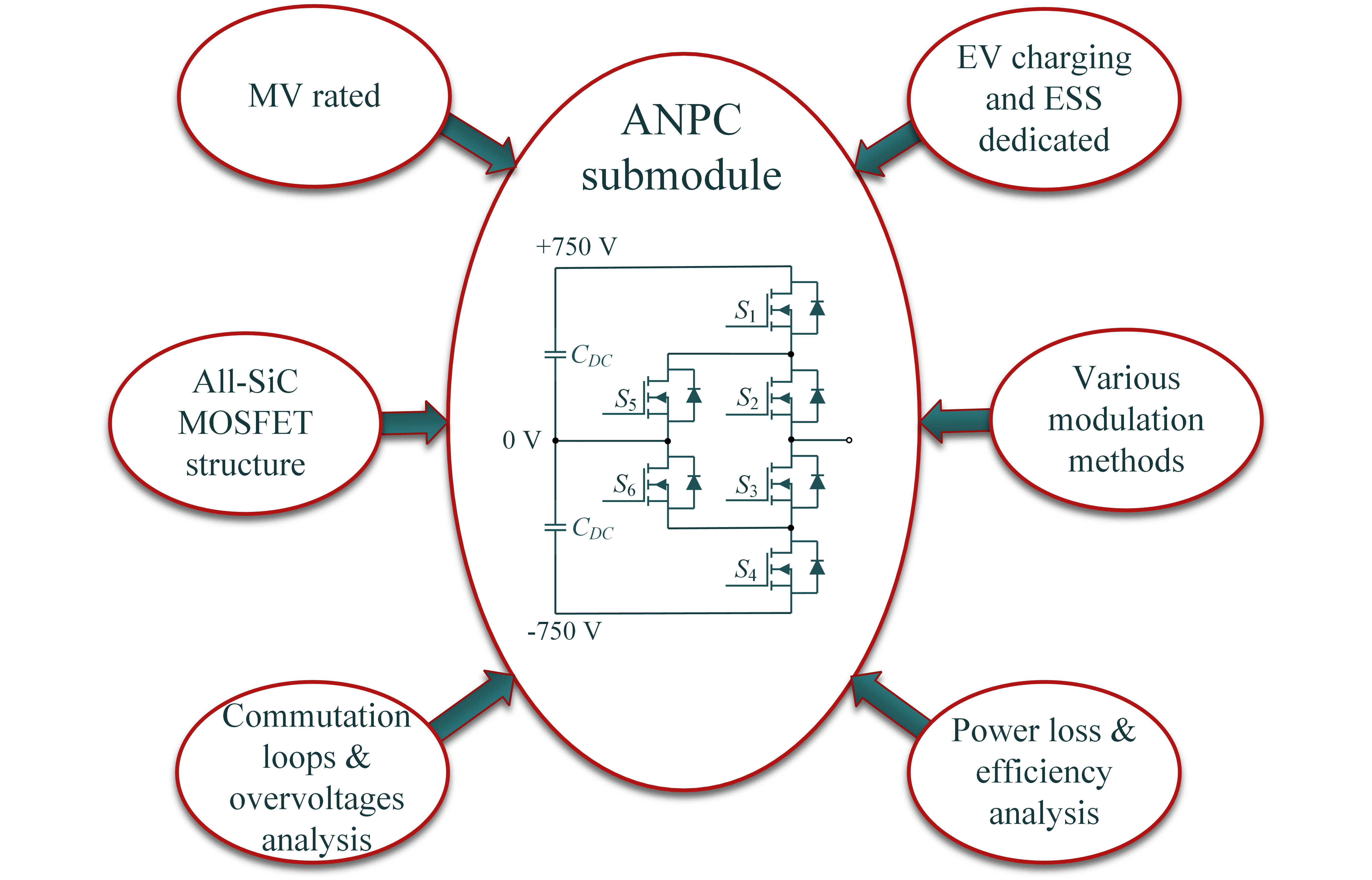
All-SiC ANPC Submodule for an Advanced 1.5 kV EV Charging System under Various Modulation Methods


Abstract
: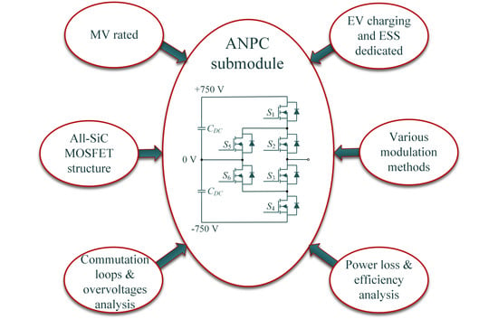
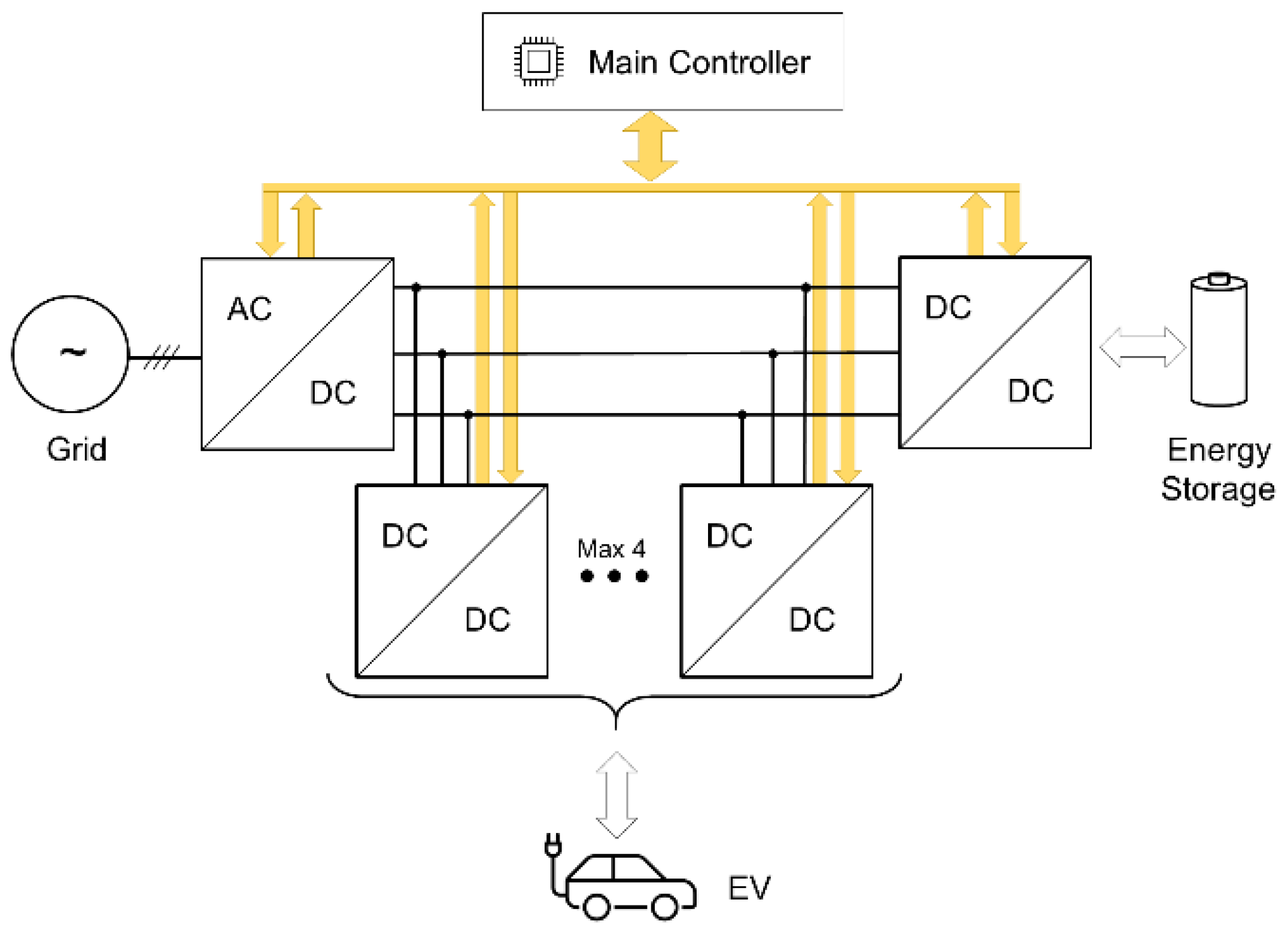
1. Introduction
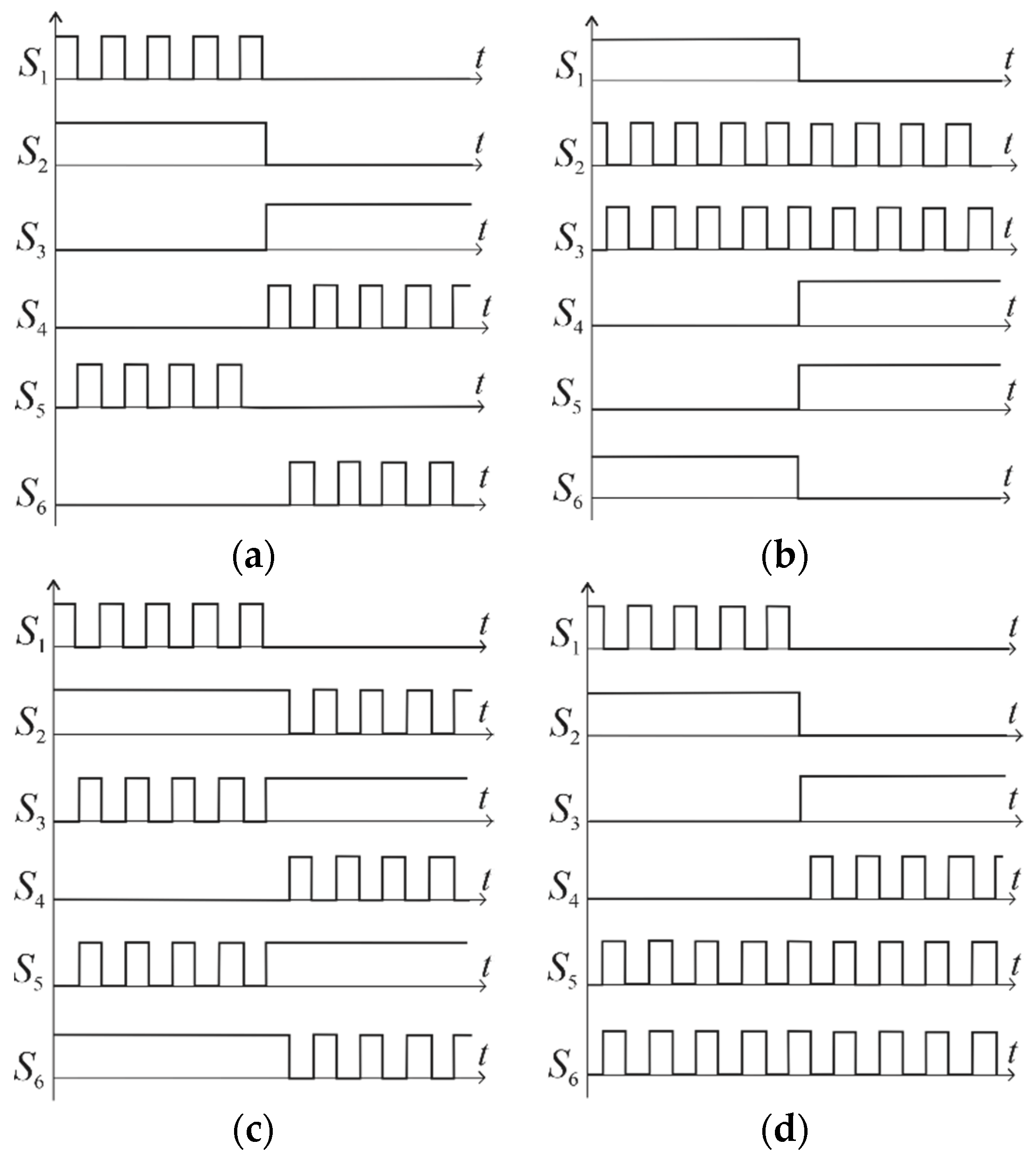
2. Modulation Strategies in Active Neutral Point Clamped (Anpc) Converter
3. Simulation Study
4. Experimental Study
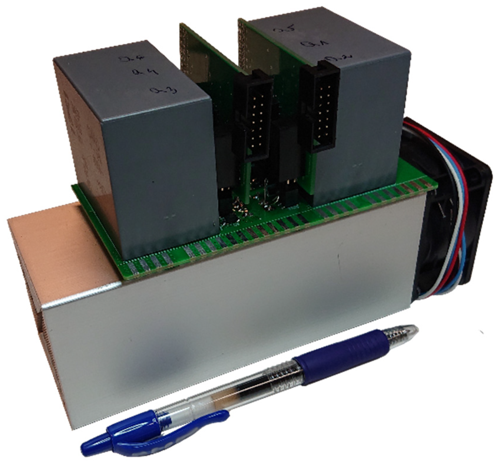
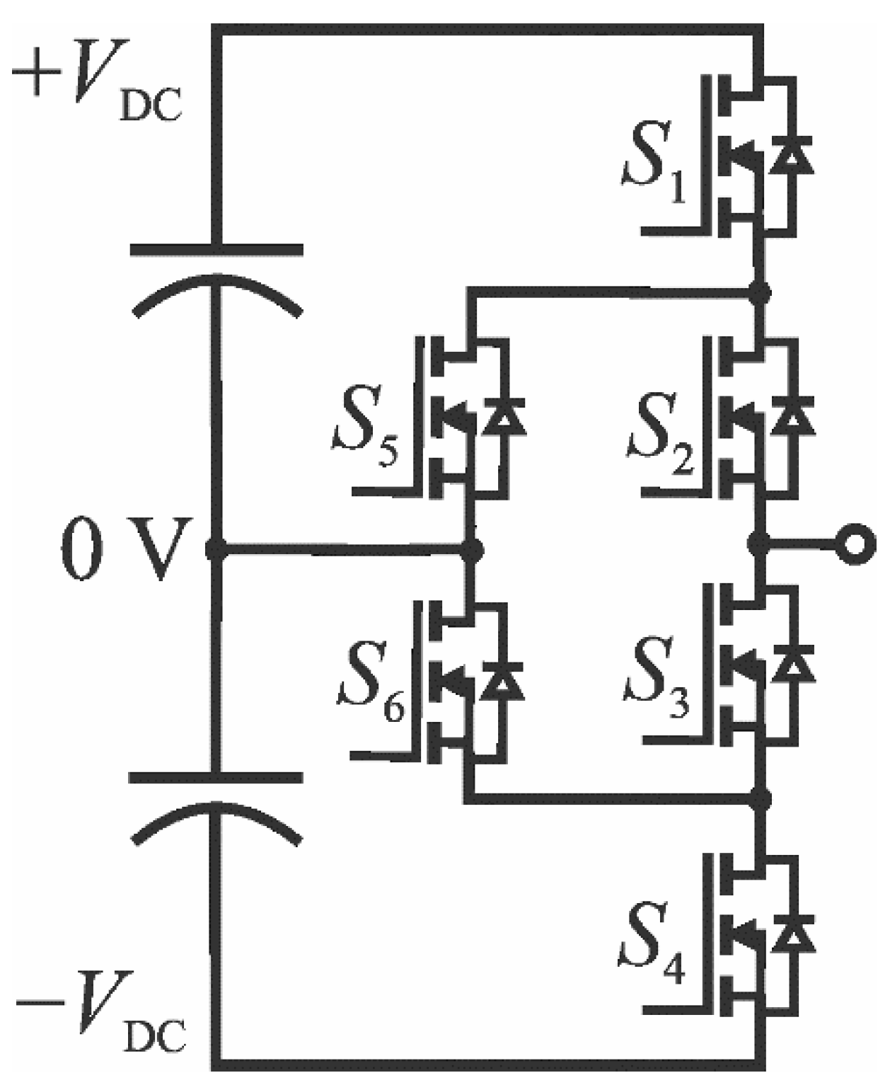
4.1. The ANPC Submodule Prototype
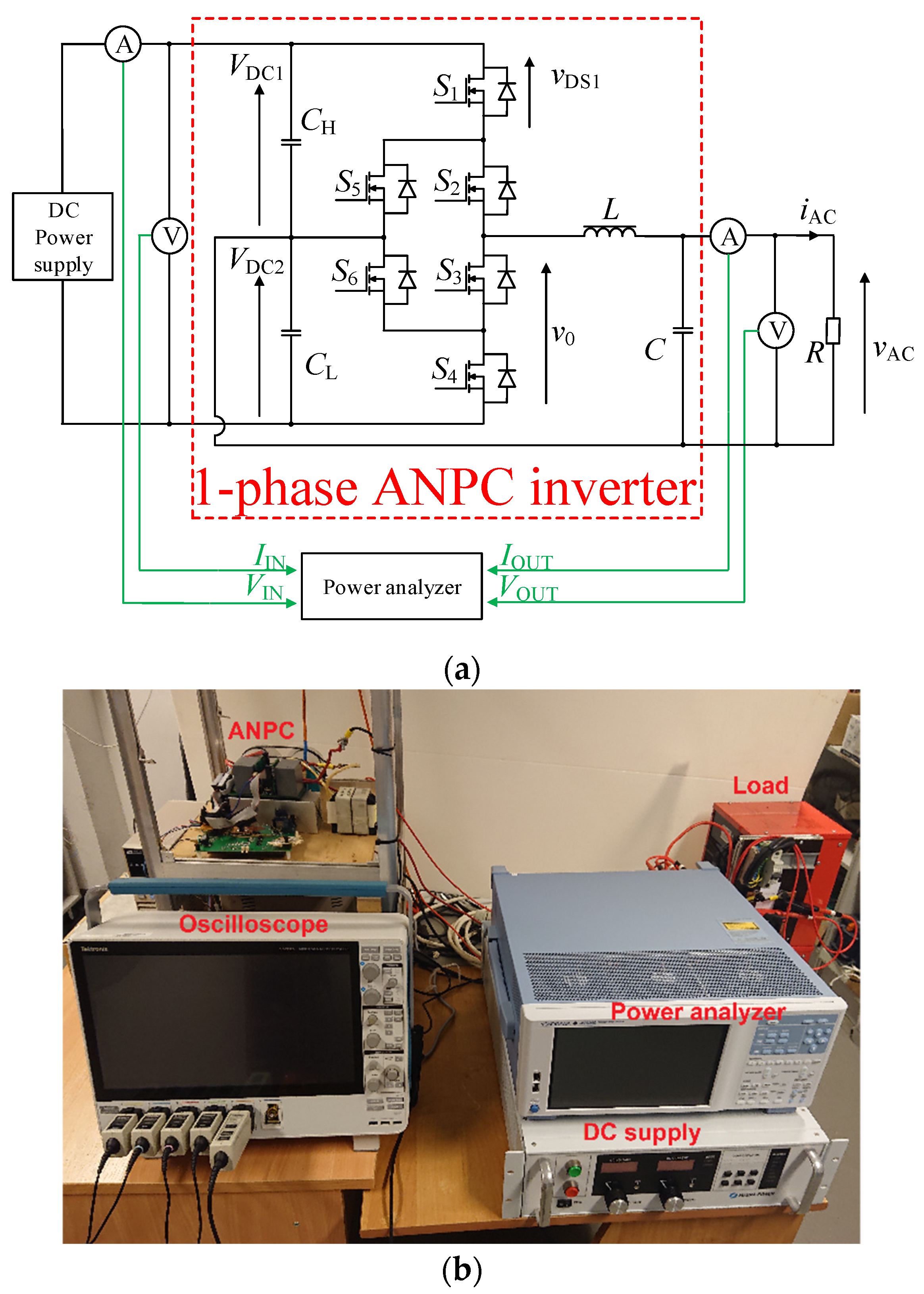
4.2. Experimental Setup
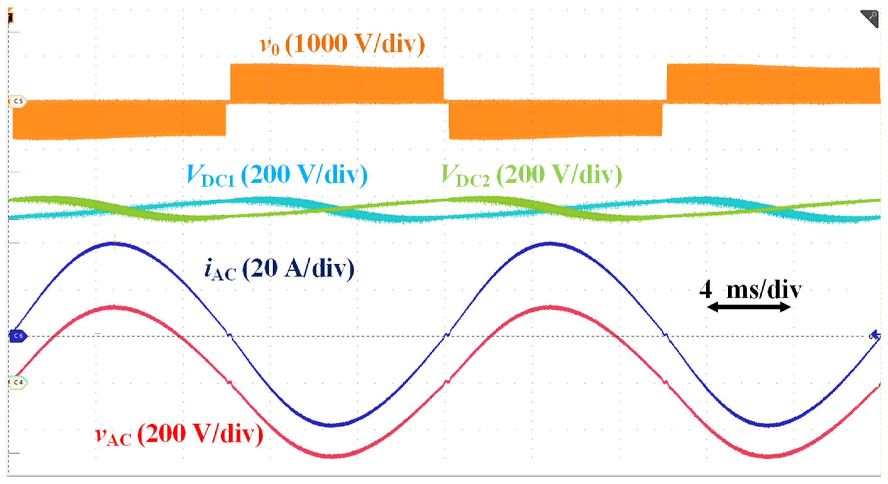
4.3. Results from the Experimental Study
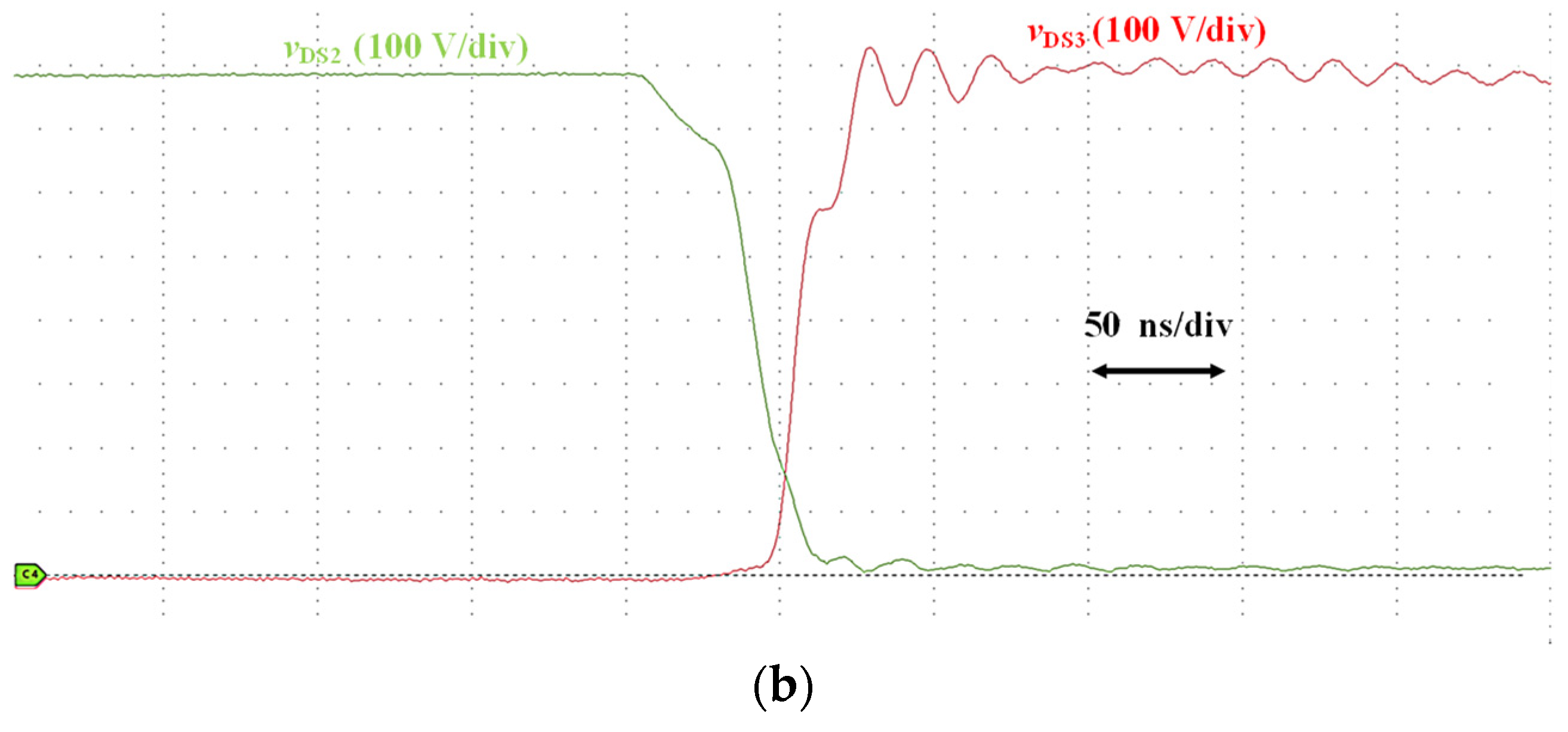
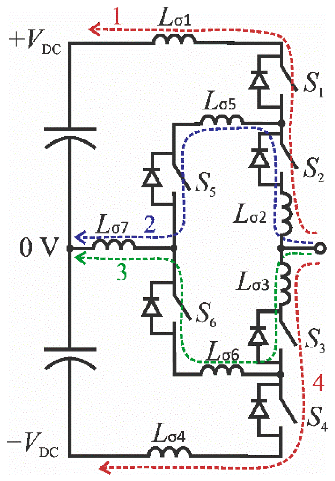
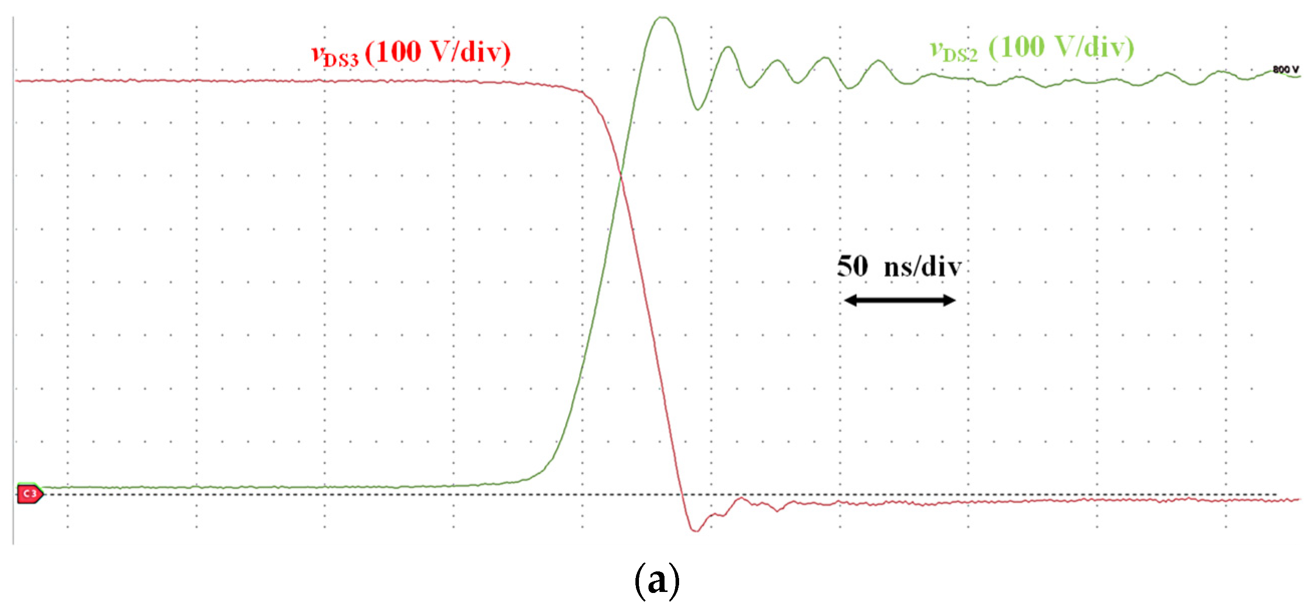
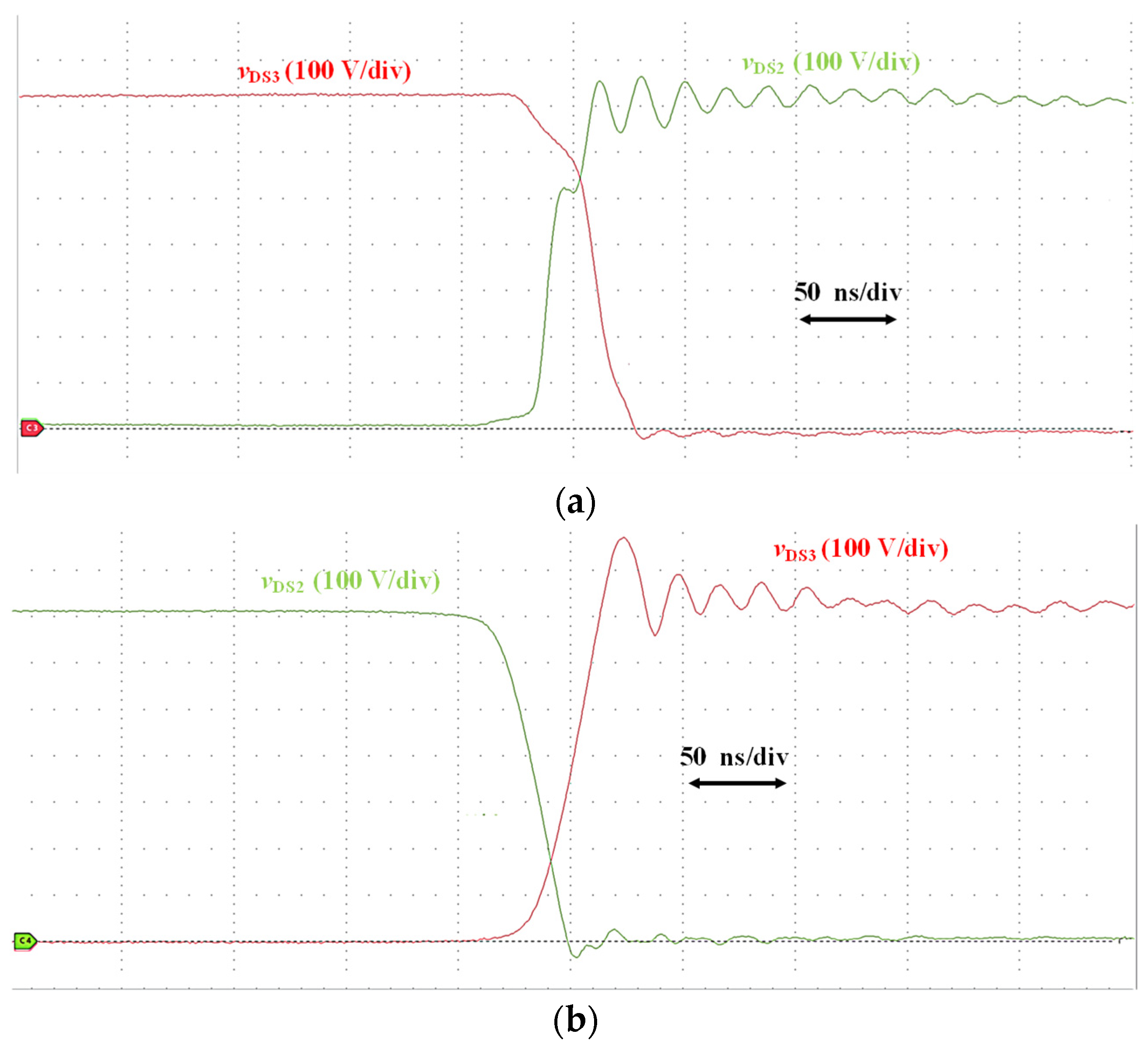
4.3.1. Transistor Overvoltage and Ringing
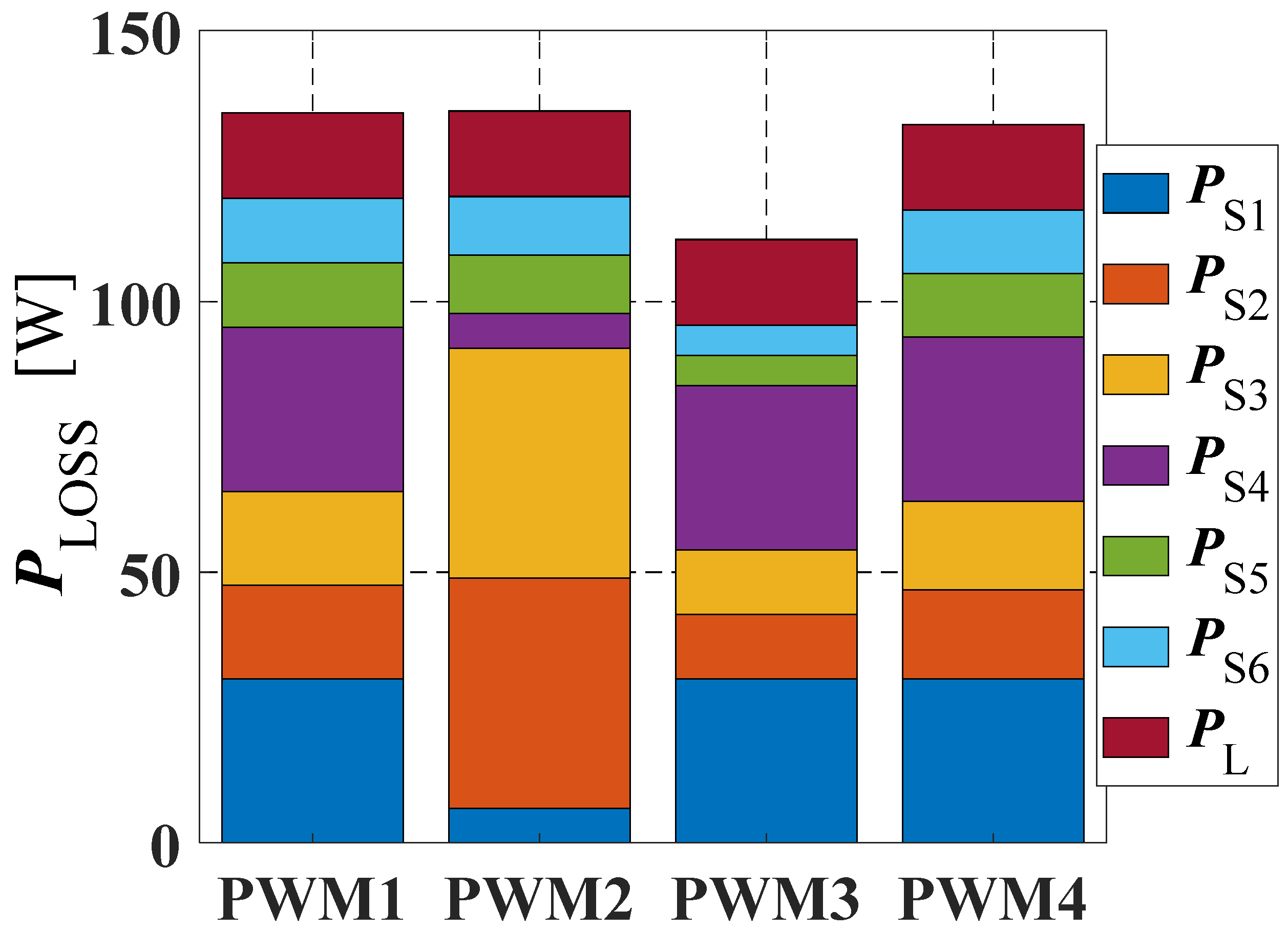
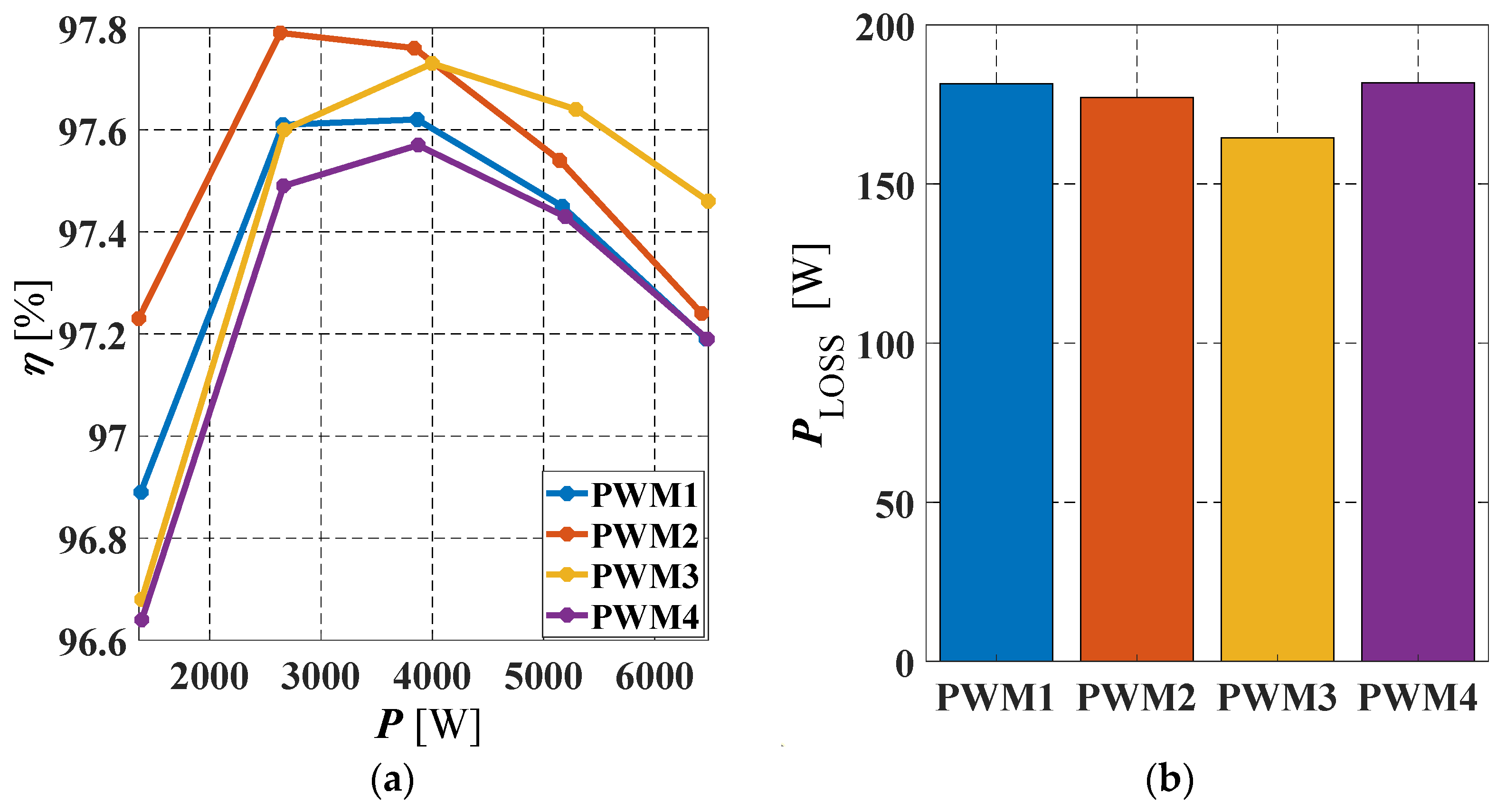
4.3.2. Power Losses
5. Conclusions
Author Contributions
Funding
Institutional Review Board Statement
Informed Consent Statement
Conflicts of Interest
References
- Rivera, S.; Kouro, S.; Vazquez, S.; Goetz, S.M.; Lizana, R.; Romero-Cadaval, E. Electric Vehicle Charging Infrastructure: From Grid to Battery. IEEE Ind. Electron. Mag. 2021, 15, 37–51. [Google Scholar] [CrossRef]
- Ghosh, A. Possibilities and Challenges for the Inclusion of the Electric Vehicle (EV) to Reduce the Carbon Footprint in the Transport Sector: A Review. Energies 2020, 13, 2602. [Google Scholar] [CrossRef]
- Ronanki, D.; Kelkar, A.; Williamson, S.S. Extreme Fast Charging Technology—Prospects to Enhance Sustainable Electric Transportation. Energies 2019, 12, 3721. [Google Scholar] [CrossRef] [Green Version]
- Hussain, A.; Bui, V.-H.; Baek, J.-W.; Kim, H.-M. Stationary Energy Storage System for Fast EV Charging Stations: Simultaneous Sizing of Battery and Converter. Energies 2019, 12, 4516. [Google Scholar] [CrossRef] [Green Version]
- Rafi, M.A.H.; Bauman, J. A Comprehensive Review of DC Fast-Charging Stations With Energy Storage: Architectures, Power Converters, and Analysis. IEEE Trans. Transp. Electrif. 2021, 7, 345–368. [Google Scholar] [CrossRef]
- Rivera, S.; Lizana, R.; Kouro, S.; Dragičević, T.; Wu, B. Bipolar DC Power Conversion: State-of-the-Art and Emerging Technologies. IEEE J. Emerg. Sel. Top. Power Electron. 2021, 9, 1192–1204. [Google Scholar] [CrossRef]
- Tahir, Y.; Khan, I.; Rahman, S.; Nadeem, M.F.; Iqbal, A.; Xu, Y.; Rafi, M. A state-of-the-art review on topologies and control techniques of solid-state transformers for electric vehicle extreme fast charging. IET Power Electron. 2021, 14, 1560–1576. [Google Scholar] [CrossRef]
- Poorfakhraei, A.; Narimani, M.; Emadi, A. A Review of Multilevel Inverter Topologies in Electric Vehicles: Current Status and Future Trends. IEEE Open J. Power Electron. 2021, 2, 155–170. [Google Scholar] [CrossRef]
- Bruckner, T.; Bemet, S. Loss balancing in three-level voltage source inverters applying active NPC switches. In Proceedings of the 2001 IEEE 32nd Annual Power Electronics Specialists Conference (IEEE Cat. No.01CH37230), Vancouver, BC, Canada, 17–21 June 2001; Volume 1132, pp. 1135–1140. [Google Scholar]
- Ma, L.; Kerekes, T.; Rodriguez, P.; Jin, X.; Teodorescu, R.; Liserre, M. A New PWM Strategy for Grid-Connected Half-Bridge Active NPC Converters With Losses Distribution Balancing Mechanism. IEEE Trans. Power Electron. 2015, 30, 5331–5340. [Google Scholar] [CrossRef] [Green Version]
- Bruckner, T.; Bernet, S.; Guldner, H. The active NPC converter and its loss-balancing control. IEEE Trans. Ind. Electron. 2005, 52, 855–868. [Google Scholar] [CrossRef]
- Schweizer, M.; Kolar, J.W. Design and Implementation of a Highly Efficient Three-Level T-Type Converter for Low-Voltage Applications. IEEE Trans. Power Electron. 2013, 28, 899–907. [Google Scholar] [CrossRef]
- Ronanki, D.; Williamson, S.S. Modular Multilevel Converters for Transportation Electrification: Challenges and Opportunities. IEEE Trans. Transp. Electrif. 2018, 4, 399–407. [Google Scholar] [CrossRef]
- Teston, S.A.; Vilerá, K.V.; Mezaroba, M.; Rech, C. Control System Development for the Three-Ports ANPC Converter. Energies 2020, 13, 3967. [Google Scholar] [CrossRef]
- Lara, J.; Masisi, L.; Hernandez, C.; Arjona, M.A.; Chandra, A. Novel Five-Level ANPC Bidirectional Converter for Power Quality Enhancement during G2V/V2G Operation of Cascaded EV Charger. Energies 2021, 14, 2650. [Google Scholar] [CrossRef]
- Rabkowski, J.; Peftitsis, D.; Nee, H. Silicon carbide power transistors: A new era in power electronics is initiated. IEEE Ind. Electron. Mag. 2012, 6, 17–26. [Google Scholar] [CrossRef]
- Biela, J.; Schweizer, M.; Waffler, S.; Kolar, J.W. Sic versus si—Evaluation of potentials for performance improvement of inverter and dc–dc converter systems by sic power semiconductors. IEEE Trans. Ind. Electron. 2011, 58, 2872–2882. [Google Scholar] [CrossRef]
- Feng, Z.; Zhang, X.; Yu, S.; Zhuang, J. Comparative Study of 2SiC&4Si Hybrid Configuration Schemes in ANPC Inverter. IEEE Access 2020, 8, 33934–33943. [Google Scholar] [CrossRef]
- Zhang, L.; Lou, X.; Li, C.; Wu, F.; Gu, Y.; Chen, G.; Xu, D. Evaluation of Different Si/SiC Hybrid Three-Level Active NPC Inverters for High Power Density. IEEE Trans. Power Electron. 2020, 35, 8224–8236. [Google Scholar] [CrossRef]
- Feng, Z.; Zhang, X.; Wang, J.; Yu, S. A High-Efficiency Three-Level ANPC Inverter Based on Hybrid SiC and Si Devices. Energies 2020, 13, 1159. [Google Scholar] [CrossRef] [Green Version]
- Zhang, L.; Liu, S.; Chen, G.; Yang, X. Evaluation of Hybrid Si/SiC Three-Level Active Neutral-Point-Clamped Inverters. In Proceedings of the 2019 IEEE 28th International Symposium on Industrial Electronics (ISIE), Vancouver, BC, Canada, 12–14 June 2019; pp. 840–845. [Google Scholar] [CrossRef]
- Zhang, D.; He, J.; Pan, D. A Megawatt-Scale Medium-Voltage High Efficiency High Power Density “SiC+Si” Hybrid Three-Level ANPC Inverter for Aircraft Hybrid-Electric Propulsion Systems. In Proceedings of the 2018 IEEE Energy Conversion Congress and Exposition (ECCE), Portland, OR, USA, 23–27 September 2018; pp. 806–813. [Google Scholar]
- Jiao, Y.; Lee, F.C. New Modulation Scheme for Three-Level Active Neutral-Point-Clamped Converter with Loss and Stress Reduction. IEEE Trans. Ind. Electron. 2015, 62, 5468–5479. [Google Scholar] [CrossRef]
- Floricau, D.; Gateau, G.; Leredde, A.; Teodorescu, R. The efficiency of three-level Active NPC converter for different PWM strategies. In Proceedings of the 2009 13th European Conference on Power Electronics and Applications, Barcelona, Spain, 8–10 September 2009; pp. 1–9. [Google Scholar]
- Belkhode, S.; Shukla, A.; Doolla, S. Enhanced Hybrid Active-Neutral-Point-Clamped Converter With Optimized Loss Distribution-Based Modulation Scheme. IEEE Trans. Power Electron. 2021, 36, 3600–3612. [Google Scholar] [CrossRef]
- Mayor, A.; Rizo, M.; Monter, A.R.; Bueno, E.J. Commutation Behavior Analysis of a Dual 3L-ANPC-VSC Phase-Leg PEBB Using 4.5-kV and 1.5-kA HV-IGBT Modules. IEEE Trans. Power Electron. 2019, 34, 1125–1141. [Google Scholar] [CrossRef]
- Jiao, Y.; Lu, S.; Lee, F.C. Switching Performance Optimization of a High Power High Frequency Three-Level Active Neutral Point Clamped Phase Leg. IEEE Trans. Power Electron. 2014, 29, 3255–3266. [Google Scholar] [CrossRef]
- Apeldoorn, O.; Odegard, B.; Steimer, P.; Bernet, S. A 16 MVA ANPC-PEBB with 6 kA IGCTs. In Proceedings of the Fourtieth IAS Annual Meeting. Conference Record of the 2005 Industry Applications Conference, Kowloon, Hong Kong, China, 2–6 October 2005; Volume 812, pp. 818–824. [Google Scholar]
- Chen, M.; Pan, D.; Wang, H.; Wang, X.; Blaabjerg, F. Investigation of Switching Oscillations for Silicon Carbide MOSFETs in Three-Level Active Neutral-Point-Clamped Inverters. IEEE J. Emerg. Sel. Top. Power Electron. 2021, 9, 4839–4853. [Google Scholar] [CrossRef]
- Jahns, T.M.; Dai, H. The past, present, and future of power electronics integration technology in motor drives. CPSS Trans. Power Electron. Appl. 2017, 2, 197–216. [Google Scholar] [CrossRef]
- Cittanti, D.; Guacci, M.; Mirić, S.; Bojoi, R.; Kolar, J.W. Comparative Evaluation of 800V DC-Link Three-Phase Two/Three-Level SiC Inverter Concepts for Next-Generation Variable Speed Drives. In Proceedings of the 2020 23rd International Conference on Electrical Machines and Systems (ICEMS), Hamamatsu, Japan, 24–27 November 2020; pp. 1699–1704. [Google Scholar]
- Teichmann, R.; Bernet, S. A comparison of three-level converters versus two-level converters for low-voltage drives, traction, and utility applications. IEEE Trans. Ind. Appl. 2005, 41, 855–865. [Google Scholar] [CrossRef]
- Schweizer, M.; Friedli, T.; Kolar, J.W. Comparative Evaluation of Advanced Three-Phase Three-Level Inverter/Converter Topologies Against Two-Level Systems. IEEE Trans. Ind. Electron. 2013, 60, 5515–5527. [Google Scholar] [CrossRef]
- He, J.; Zhang, D.; Pan, D. An Improved PWM Strategy for “SiC+Si” Three-Level Active Neutral Point Clamped Converter in High-Power High-Frequency Applications. In Proceedings of the 2018 IEEE Energy Conversion Congress and Exposition (ECCE), Portland, OR, USA, 23–27 September 2018; pp. 5235–5241. [Google Scholar]
- Guan, Q.; Li, C.; Zhang, Y.; Wang, S.; Xu, D.D.; Li, W.; Ma, H. An Extremely High Efficient Three-Level Active Neutral-Point-Clamped Converter Comprising SiC and Si Hybrid Power Stages. IEEE Trans. Power Electron. 2018, 33, 8341–8352. [Google Scholar] [CrossRef]
- Barater, D.; Concari, C.; Buticchi, G.; Gurpinar, E.; De, D.; Castellazzi, A. Performance Evaluation of a Three-Level ANPC Photovoltaic Grid-Connected Inverter With 650-V SiC Devices and Optimized PWM. IEEE Trans. Ind. Appl. 2016, 52, 2475–2485. [Google Scholar] [CrossRef] [Green Version]


| State | S1 | S2 | S3 | S4 | S5 | S6 | Conduction Path(s) | PWM Method |
|---|---|---|---|---|---|---|---|---|
| P | 1 | 1 | 0 | 0 | 0 | 1/0 | 1 | 1, 2, 3, 4 |
| 0U3 | 1 | 0 | 1 | 0 | 0 | 1 | 3 | 2 |
| 0U2 | 0 | 1 | 0 | 0 | 1 | 0 | 2 | 1 |
| 0U1 | 0 | 1 | 0 | 1 | 1 | 0 | 2 | 4 |
| 0F | 0 | 1 | 1 | 0 | 1 | 1 | 2 and 3 | 3 |
| 0L1 | 1 | 0 | 1 | 0 | 0 | 1 | 3 | 4 |
| 0L2 | 0 | 0 | 1 | 0 | 0 | 1 | 3 | 1 |
| 0L3 | 0 | 1 | 0 | 1 | 1 | 0 | 2 | 2 |
| N | 0 | 0 | 1 | 1 | 1/0 | 0 | 4 | 1, 2, 3, 4 |
| Parameter | Description |
|---|---|
| DC voltage | 1500 V |
| AC voltage | 230 V RMS/50 Hz |
| Rated power | 6.67 kVA (1/3 of 20 kVA) |
| Operating frequency | 64 kHz |
| SiC MOSFETs | NTH4L040N120SC1 |
| Filter inductor | 220 µH |
| Filter capacitor | 4.7 µF |
| DC capacitors | 2 × 610 µF |
| VDC = 1500 V; P = 6.5 kW; vAC = 230 V rms | ||||
|---|---|---|---|---|
| Parameter | PWM1 | PWM2 | PWM3 | PWM4 |
| P(S1,S4) [W] | 30.3 | 6.4 | 30.3 | 30.3 |
| P(S2,S3) [W] | 17.3 | 42.5 | 11.8 | 16.4 |
| P(S5,S6) [W] | 11.9 | 10.8 | 5.6 | 11.7 |
| VDC = 1500 V; P = 6.5 kW; vAC = 230 V rms | ||||
|---|---|---|---|---|
| Parameter | PWM1 | PWM2 | PWM3 | PWM4 |
| vDS_max(S3) [V] | 832 | 957 | 846 | 827 |
| vDS_max(S4) [V] | 889 | 802 | 868 | 873 |
| vDS_max(S6) [V] | 857 | 848 | 842 | 843 |
| PLOSS(exp.) [W] | 182 | 177 | 165 | 182 |
| PLOSS(sim.) [W] | 137 | 137 | 114 | 136 |
Publisher’s Note: MDPI stays neutral with regard to jurisdictional claims in published maps and institutional affiliations. |
© 2021 by the authors. Licensee MDPI, Basel, Switzerland. This article is an open access article distributed under the terms and conditions of the Creative Commons Attribution (CC BY) license (https://creativecommons.org/licenses/by/4.0/).
Share and Cite
Kopacz, R.; Harasimczuk, M.; Lasek, B.; Miśkiewicz, R.; Rąbkowski, J. All-SiC ANPC Submodule for an Advanced 1.5 kV EV Charging System under Various Modulation Methods. Energies 2021, 14, 5580. https://doi.org/10.3390/en14175580
Kopacz R, Harasimczuk M, Lasek B, Miśkiewicz R, Rąbkowski J. All-SiC ANPC Submodule for an Advanced 1.5 kV EV Charging System under Various Modulation Methods. Energies. 2021; 14(17):5580. https://doi.org/10.3390/en14175580
Chicago/Turabian StyleKopacz, Rafał, Michał Harasimczuk, Bartosz Lasek, Rafał Miśkiewicz, and Jacek Rąbkowski. 2021. "All-SiC ANPC Submodule for an Advanced 1.5 kV EV Charging System under Various Modulation Methods" Energies 14, no. 17: 5580. https://doi.org/10.3390/en14175580
APA StyleKopacz, R., Harasimczuk, M., Lasek, B., Miśkiewicz, R., & Rąbkowski, J. (2021). All-SiC ANPC Submodule for an Advanced 1.5 kV EV Charging System under Various Modulation Methods. Energies, 14(17), 5580. https://doi.org/10.3390/en14175580