
Implementation of a Resonant Converter with Topology Morphing to Achieve Bidirectional Power Flow

Abstract
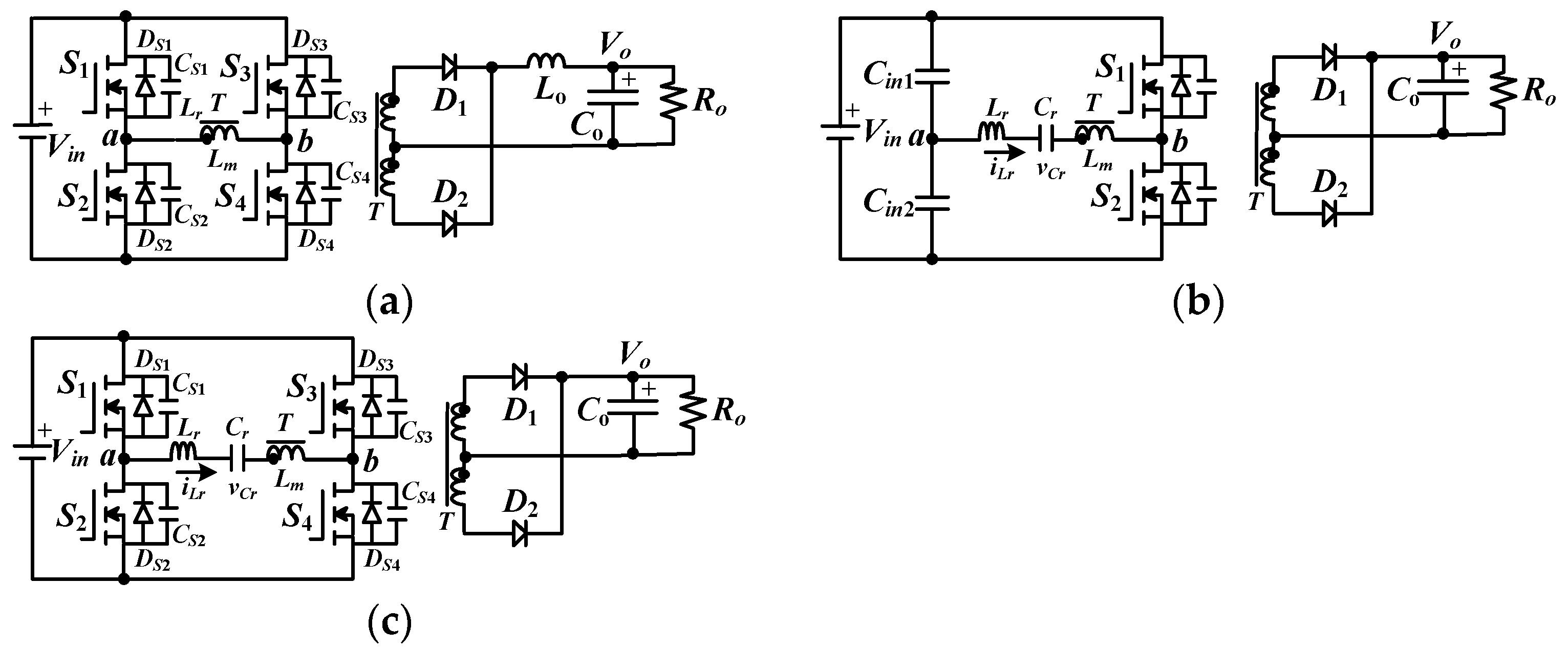
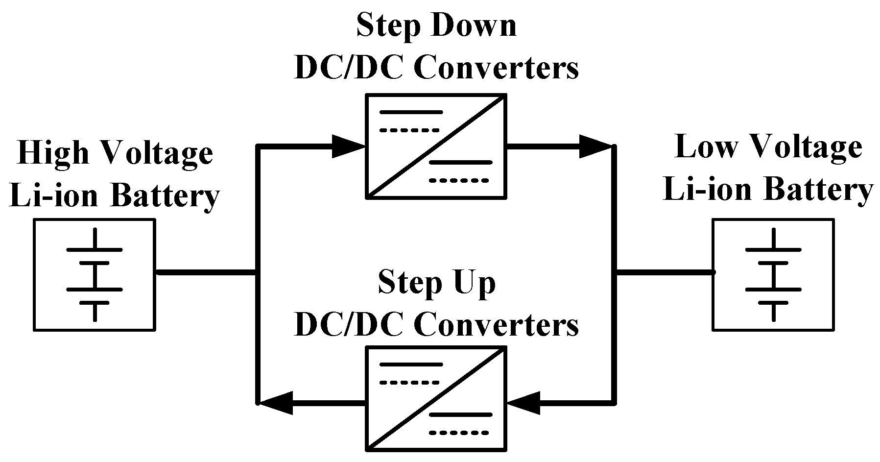
:1. Introduction
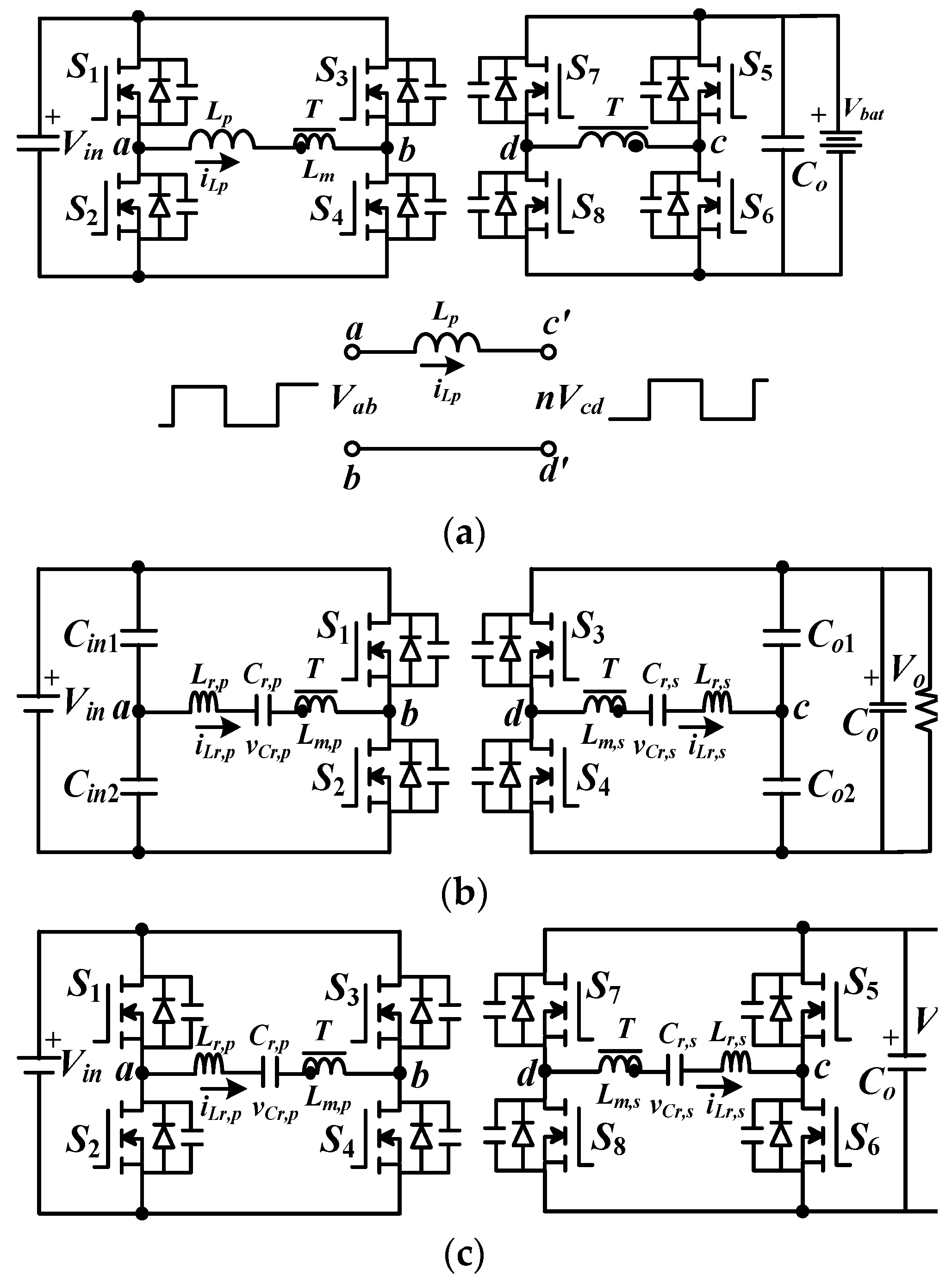
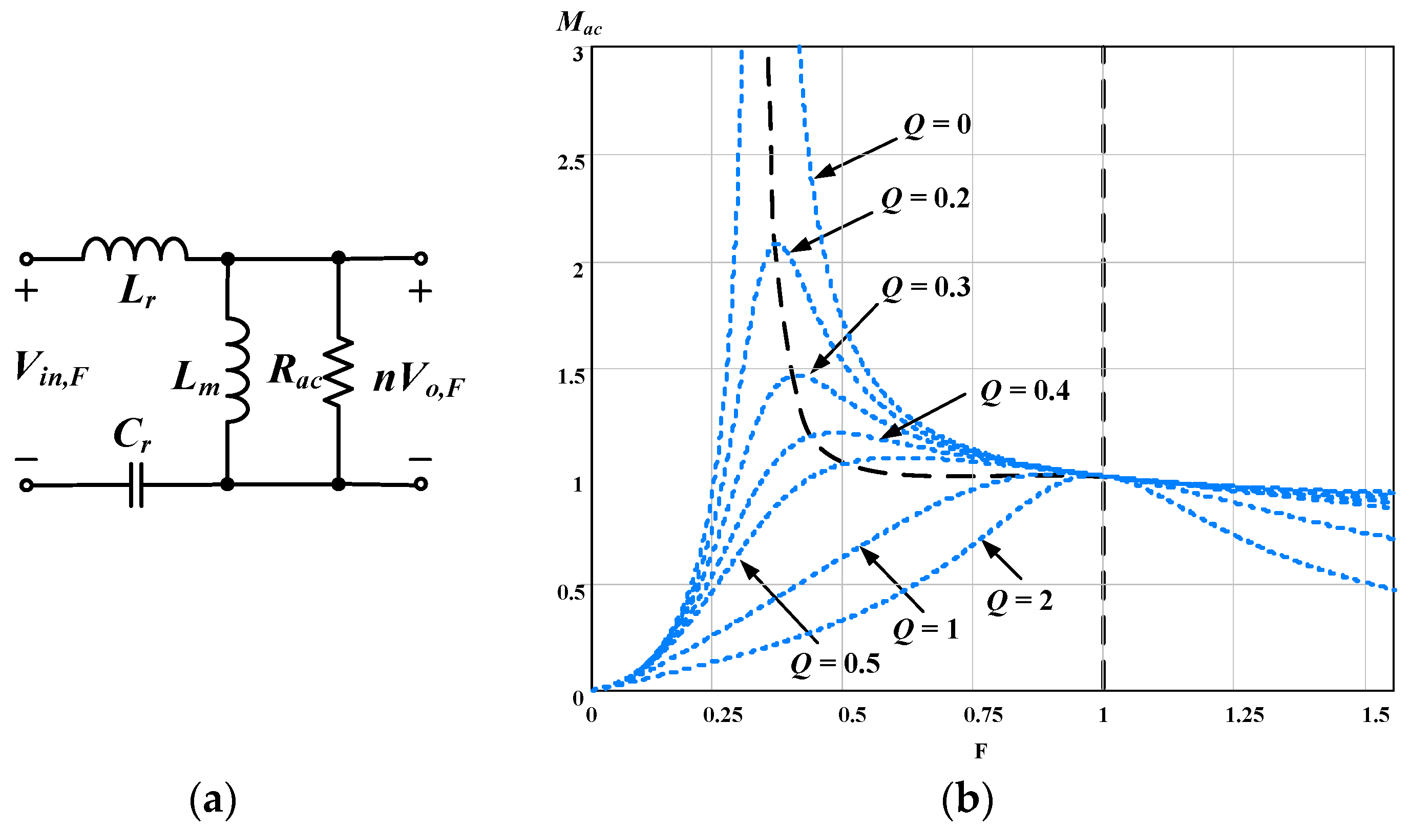
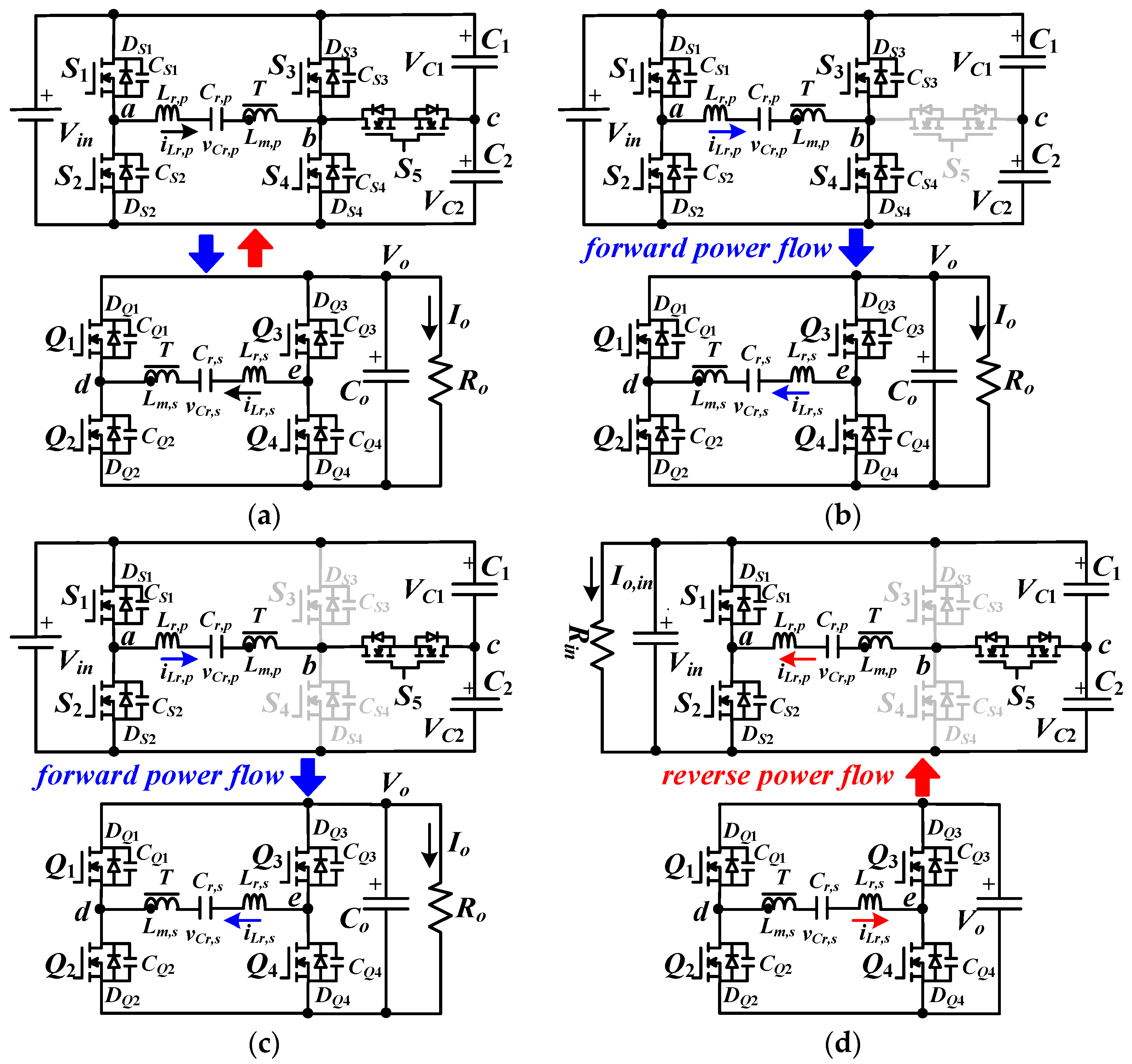
2. Circuit Schematic of the Developed Converter
3. Circuit Operation
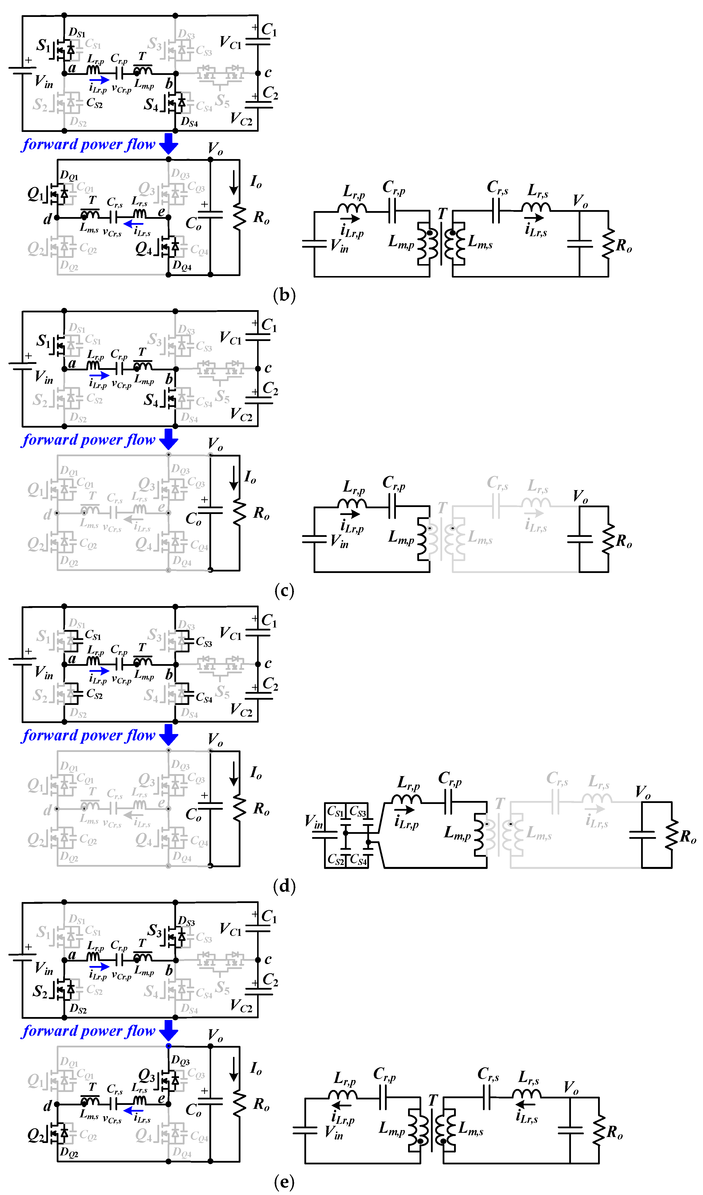
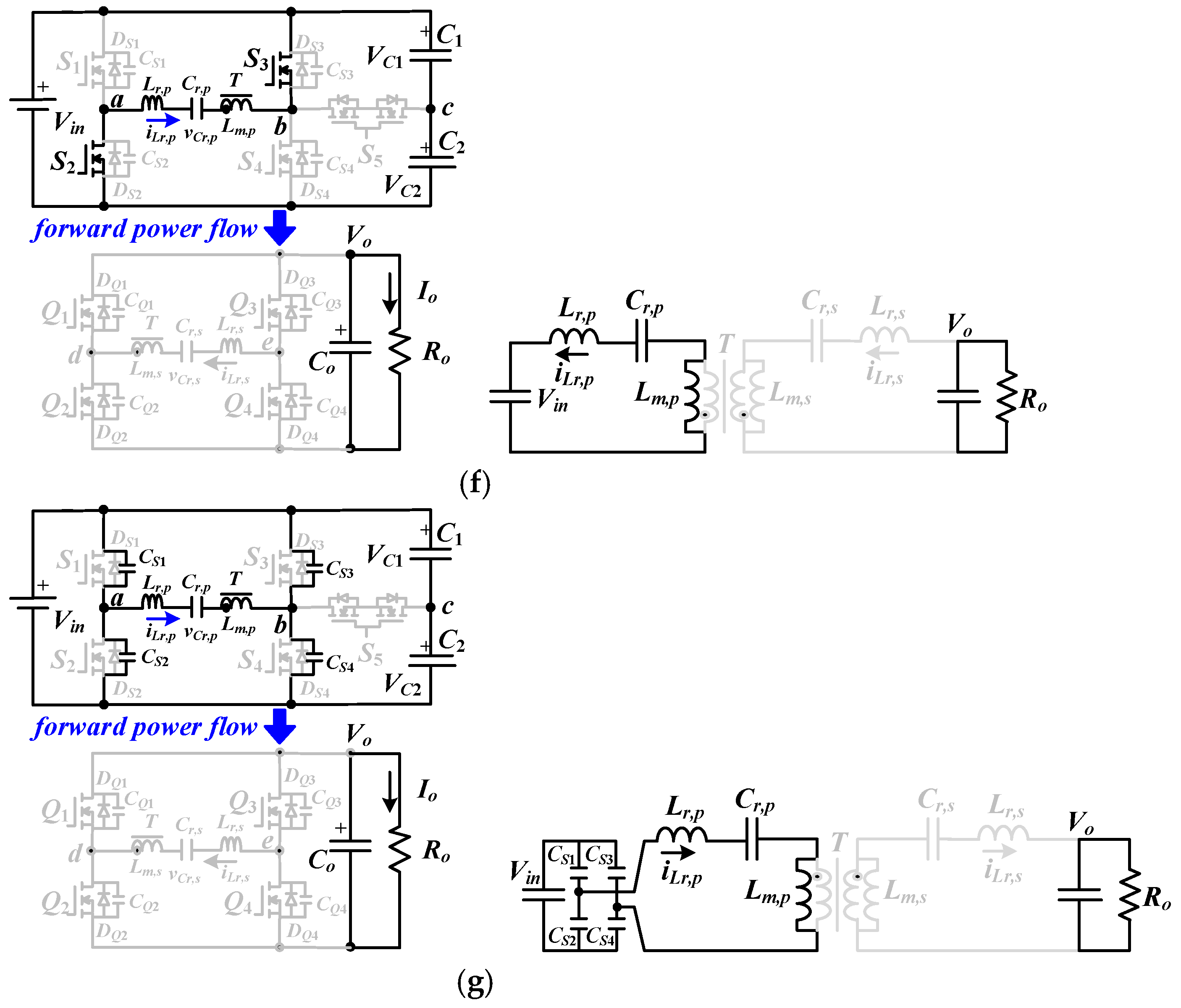
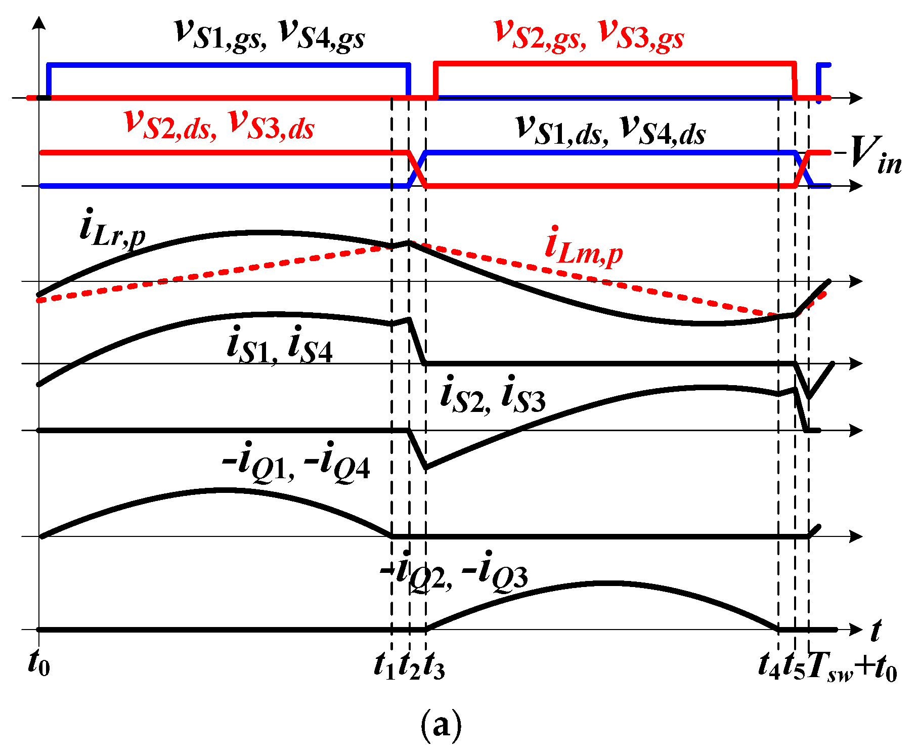
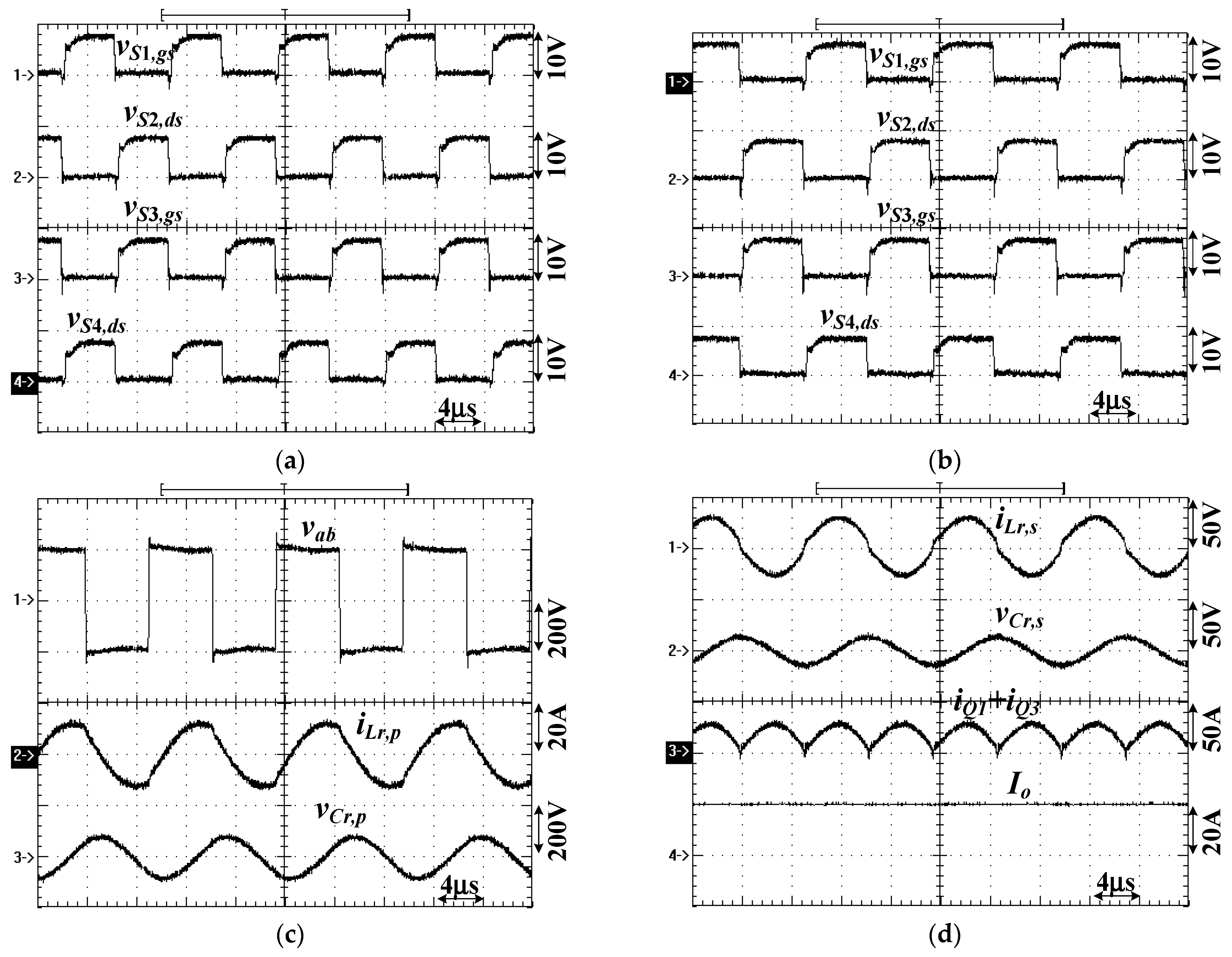
3.1. Forward Power Operation under Low Input Voltage Range
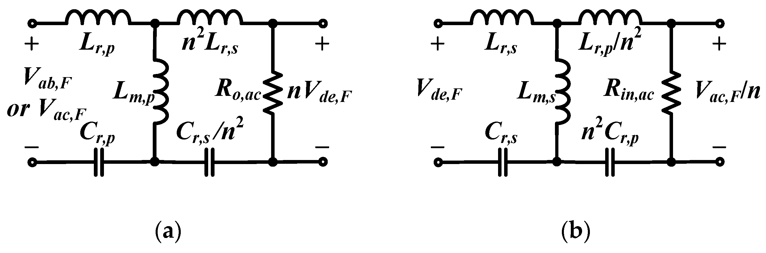
- Mode 1 [t0~t1]: At t0, S1, S4, Q1 and Q4 are on. The current iLr,p flows through S1, Lr,p, Cr,p, T and S4. The current iLr,s flows through Q4, Lr,s, Cr,s, T, Q1 and Co. Therefore, the leg voltages Vab = Vin and Vde = Vo. The resonant frequency is about . The primary and secondary currents, iLr,p and iLr,s, increase.
- Mode 2 [t1~t2]: For fr > fsw (i.e., F < 1), the secondary side current, ir,s, is decreased to 0 at t1. Then, Q1 and Q4 turn off. The resonant frequency becomes in mode two.
- Mode 3 [t2~t3]: At t2, S1 and S4 turn off and iLr,p discharges CS2 and CS3. If Equation (1) is established, vCS2 and vCS3 are 0 V at t3.where CS,eq = CS1 = CS2 = CS3 = CS4 and iLm,p,pk is the peak value of iLm,p.
- Mode4 [t3~t4]: At t3, vCS2 = vCS3 = 0 and DS2 and DS3 are forward biased due to iLr,p > 0. In this mode, S2, S3, Q2 and Q3 are on. In this mode, Vab = −Vin, Vde = −Vo and iLr,p and iLr,s both decrease.
- Mode 5 [t4~t5]: At time t4, iLr,p = iLm,p and iLr,s = 0. Thus, the synchronous switches Q3 and Q2 are off. Cr,p, Lr,p and Lm,p are resonant.
- Mode 6 [t5~Tsw + t0]: S2 and S3 turn off at t5 and iLr,p will discharge CS1 and CS4. Since CS1~CS4 are much less than Cr,p, the discharge time in mode six is fast enough to be neglected in the system analysis. The one switching cycle is ended at time Tsw + t0.
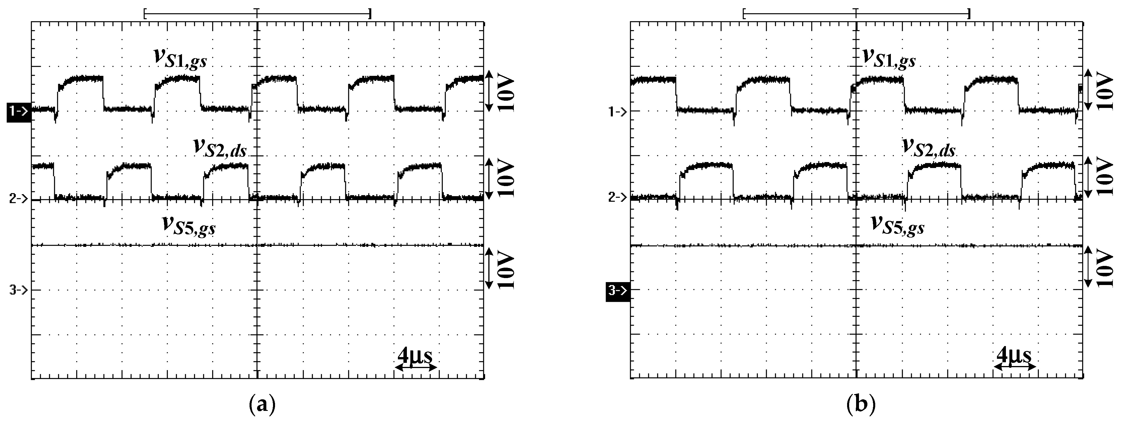
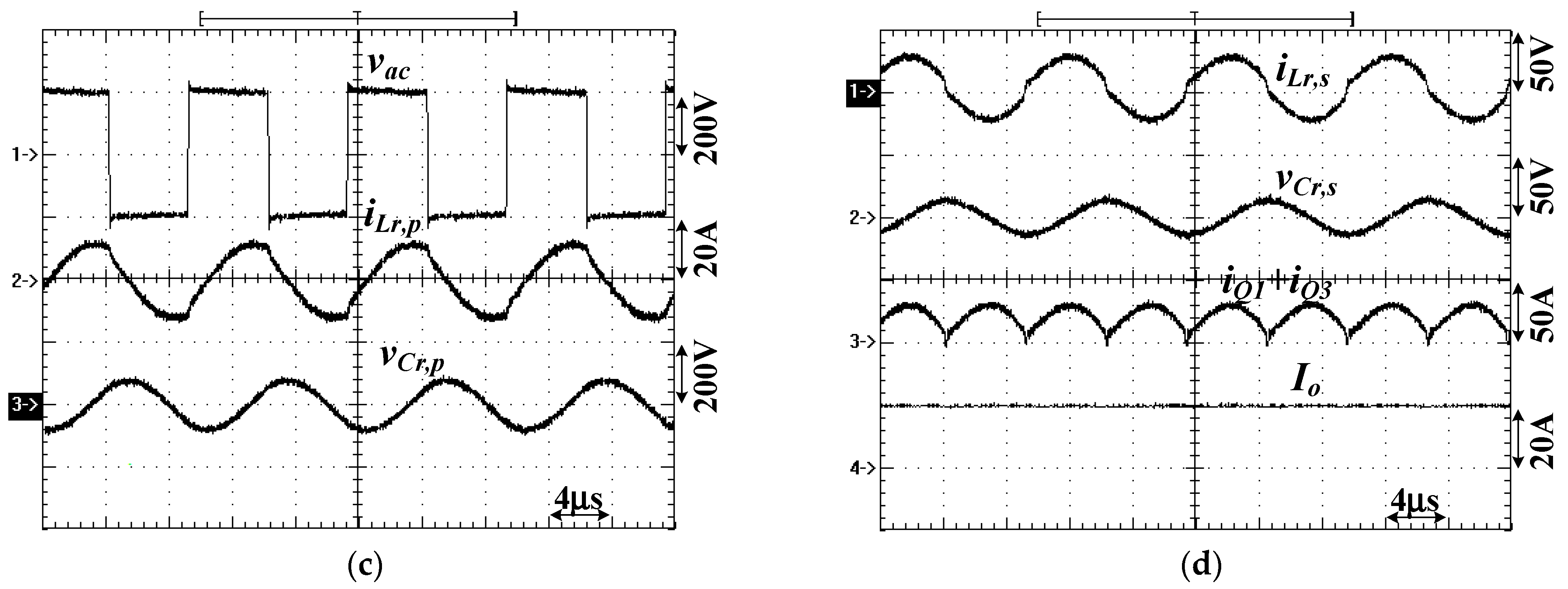
3.2. Forward Power Operation under High Input Voltage Range
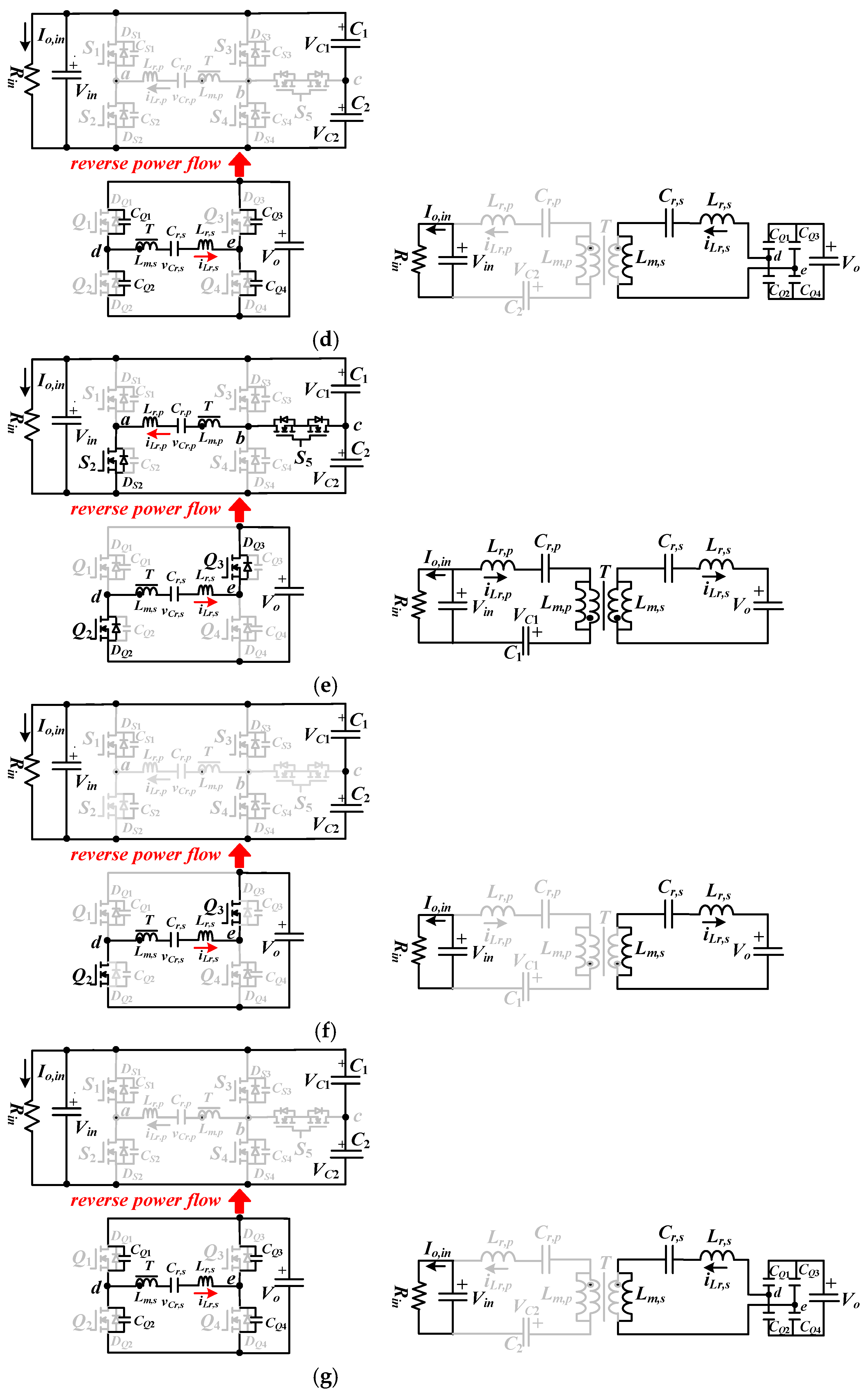
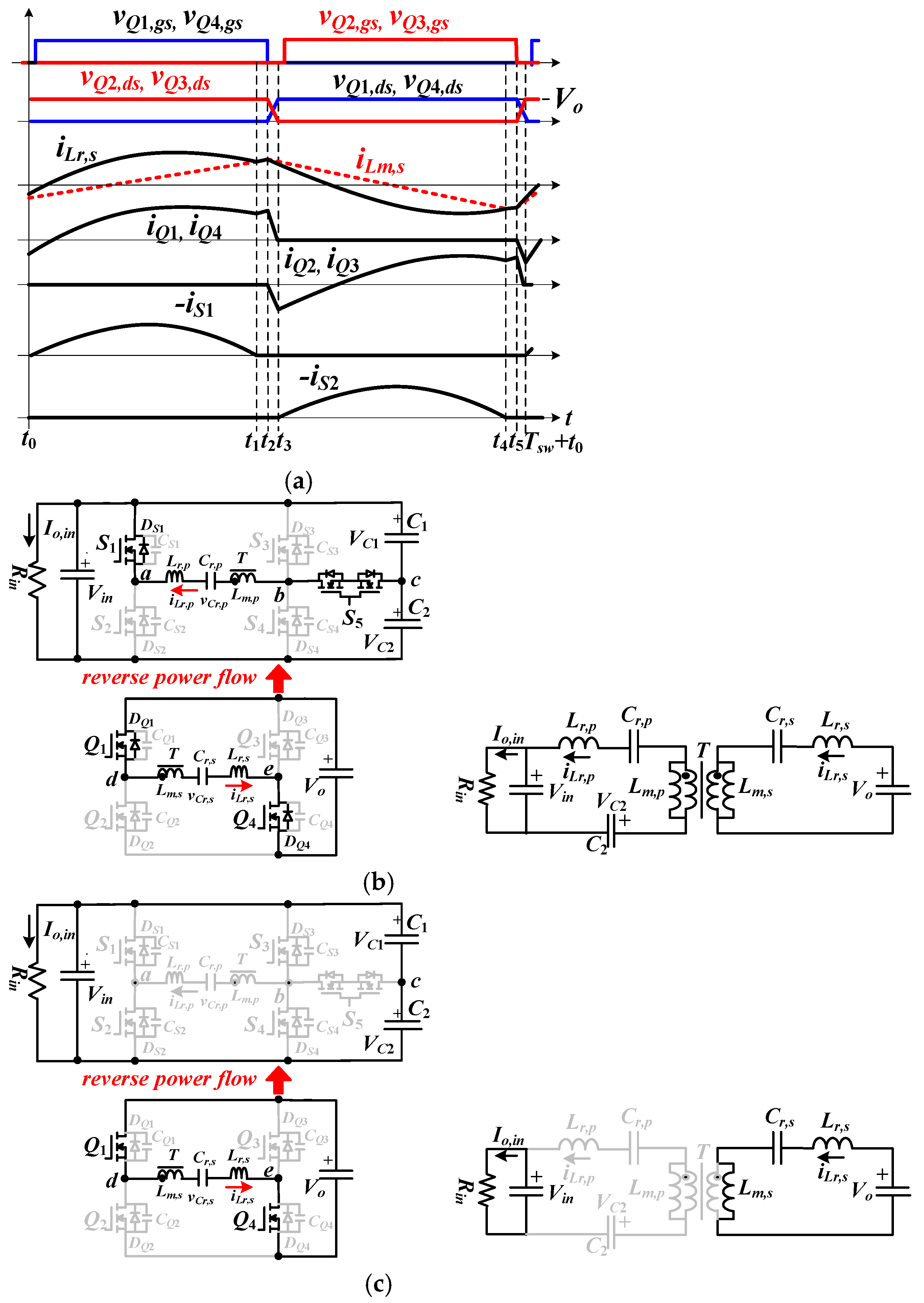
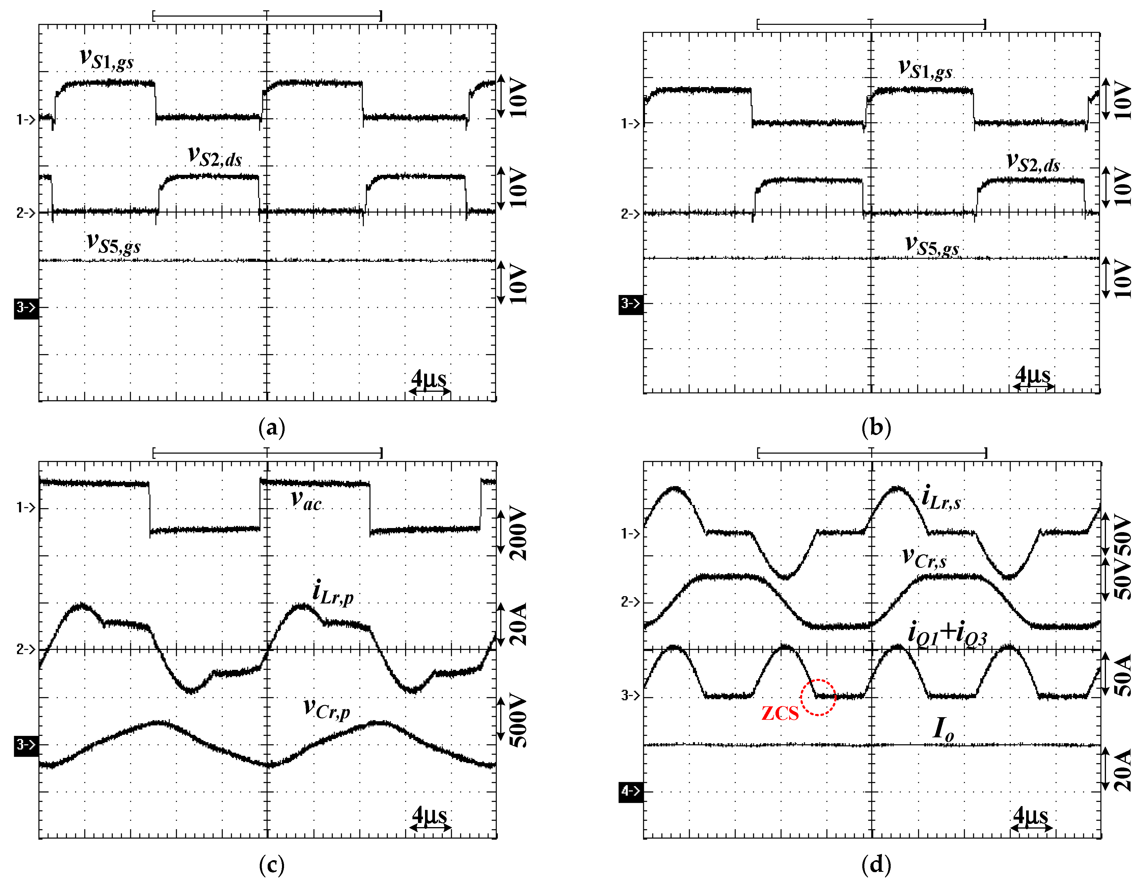
3.3. Reverse Power Operation
- Mode 1 [t0~t1]:vCQ1 = vCQ4 = 0 at t0 and iLr,s will flow through the diodes DQ1 and DQ4 due to iLr,s < 0. Therefore, active devices Q4 and Q1 turn on under zero voltage and Vde = Vo. Since iLr,p (t0) > 0, synchronous switch S1 is on and Vac = Vin.
- Mode 2 [t1~t2]: ir,p = 0 at time t1 and S1 turns off. The components Lr,s, Lm,s and Cr,s are resonant on the right-hand side of the equivalent circuit.
- Mode 3 [t2~t3]: Q1 and Q4 turn off at time t2 and iLr,s will discharge CQ2 and CQ3. CQ2 and CQ3 can be discharged to zero voltage if Equation (2) is satisfied.where CQ,eq = CQ1 = CQ2 = CQ3 = CQ4 and iLm,s,pk is the peak value of iLm,s.
- Mode4 [t3~t4]: vCQ2 and vCQ3 are decreased to 0 at t3. DQ2 and DQ3 are conducting due to iLr,s > 0. In mode four, active switches Q2, Q3 and synchronous switch S2 are on. Therefore, Vde = −Vo and Vac = −Vin.
- Mode 5 [t4~t5]: iLr,p = 0 at t4 and S2 turns off. Cr,s, Lr,s and Lm,s are resonant.
- Mode 6 [t5~Tsw + t0]: Q2 and Q3 turn off at t5 and iLr,s discharges CQ1 and CQ4 due to iLr,s < 0. At Tsw + t0, this switching cycle is completed.
4. Circuit Characteristics
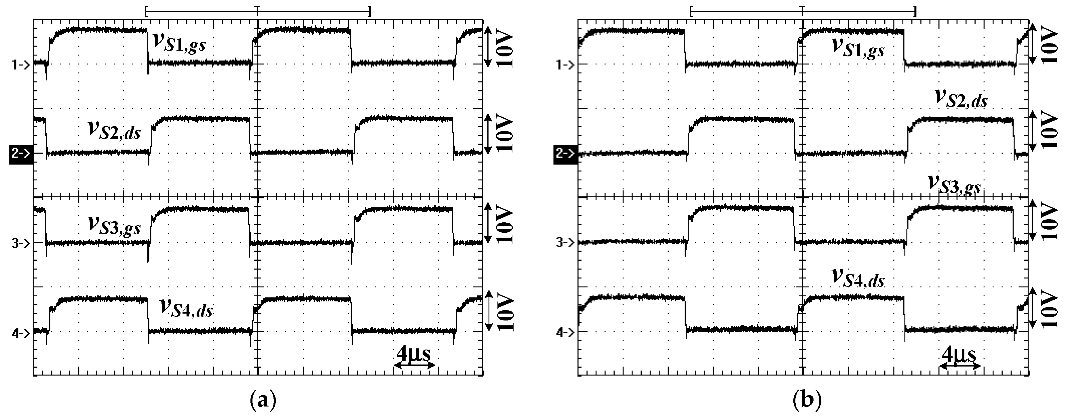
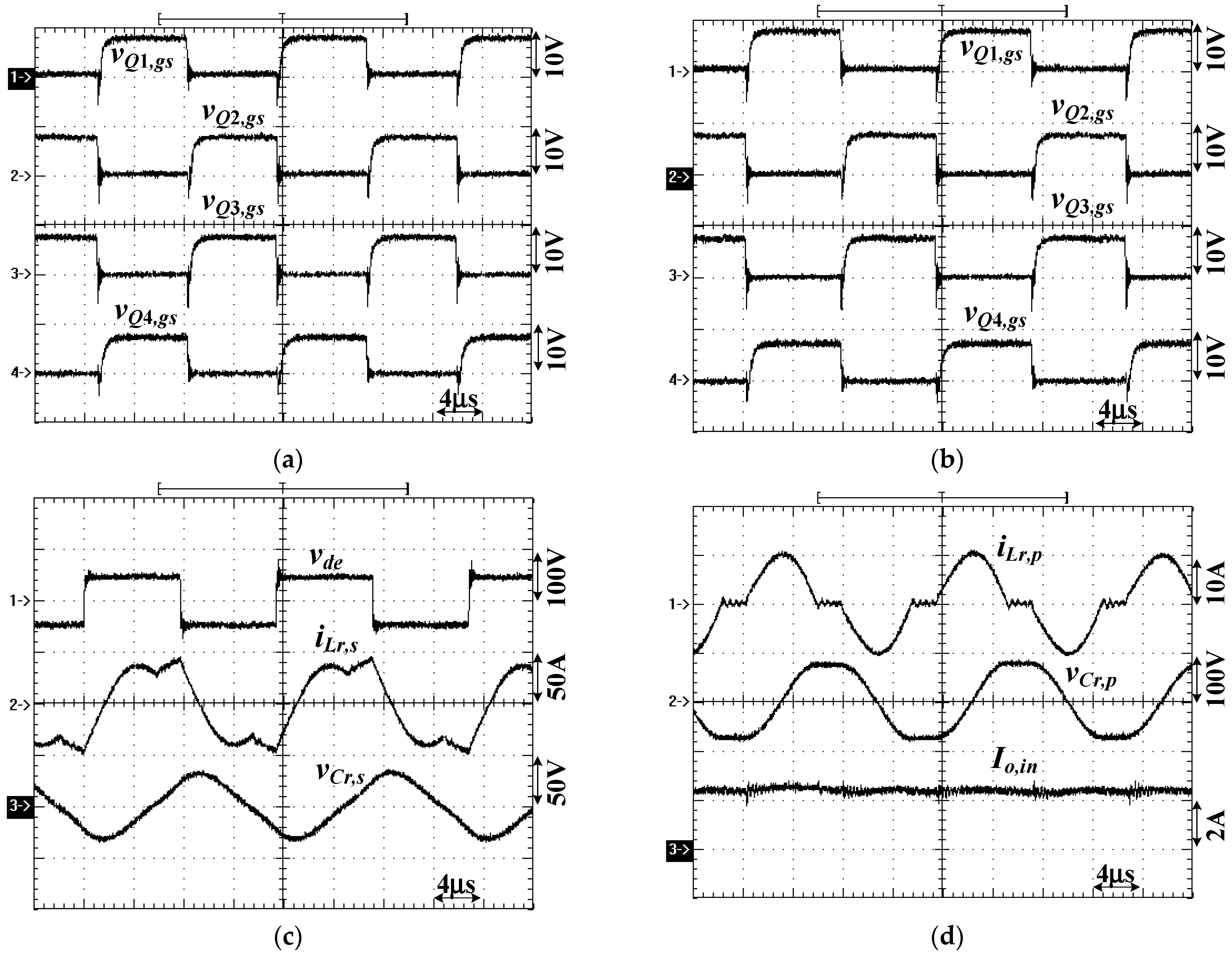
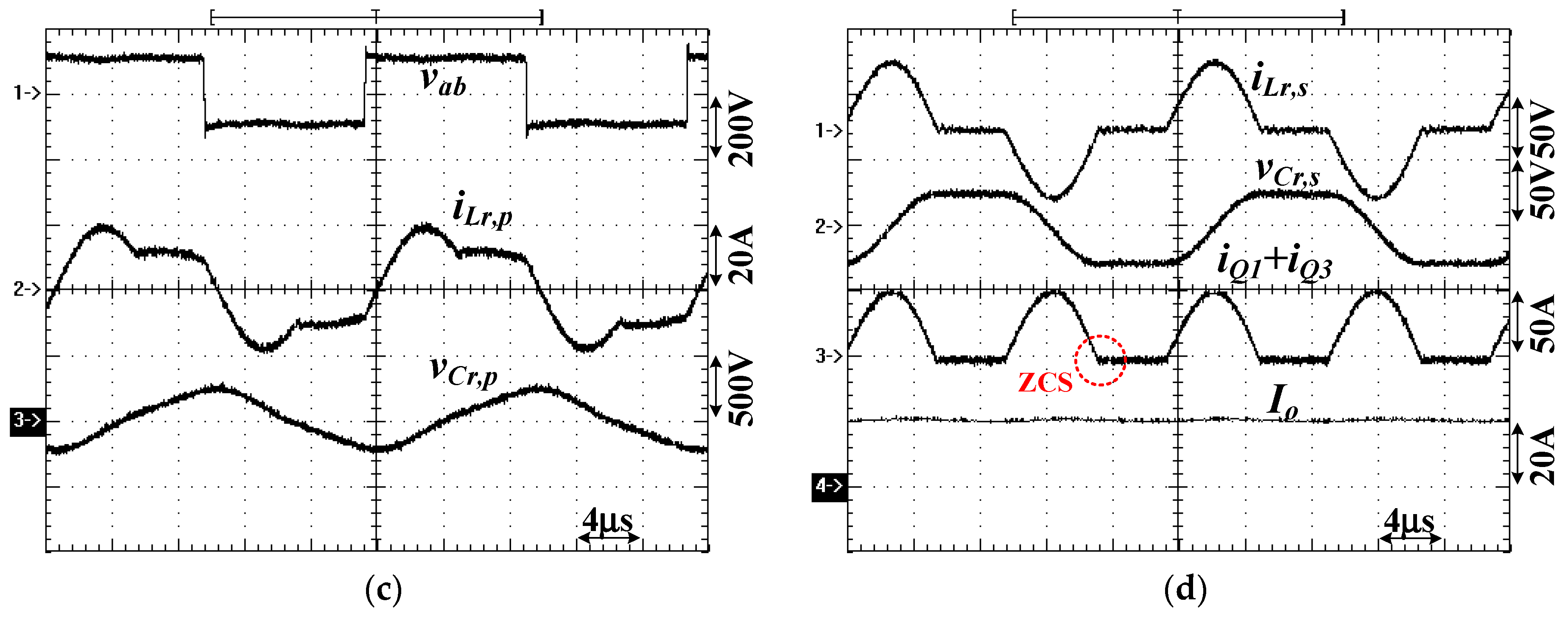
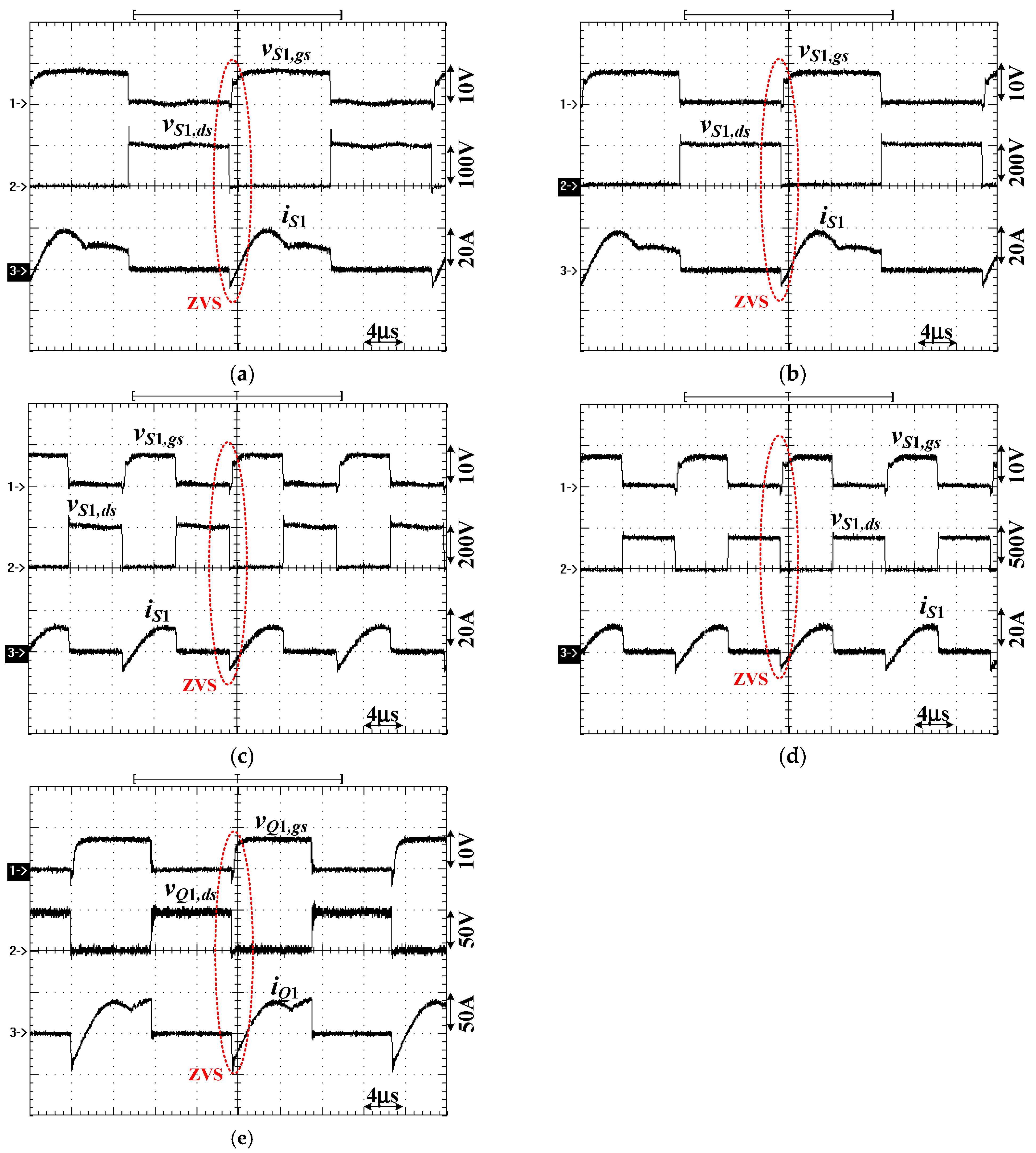
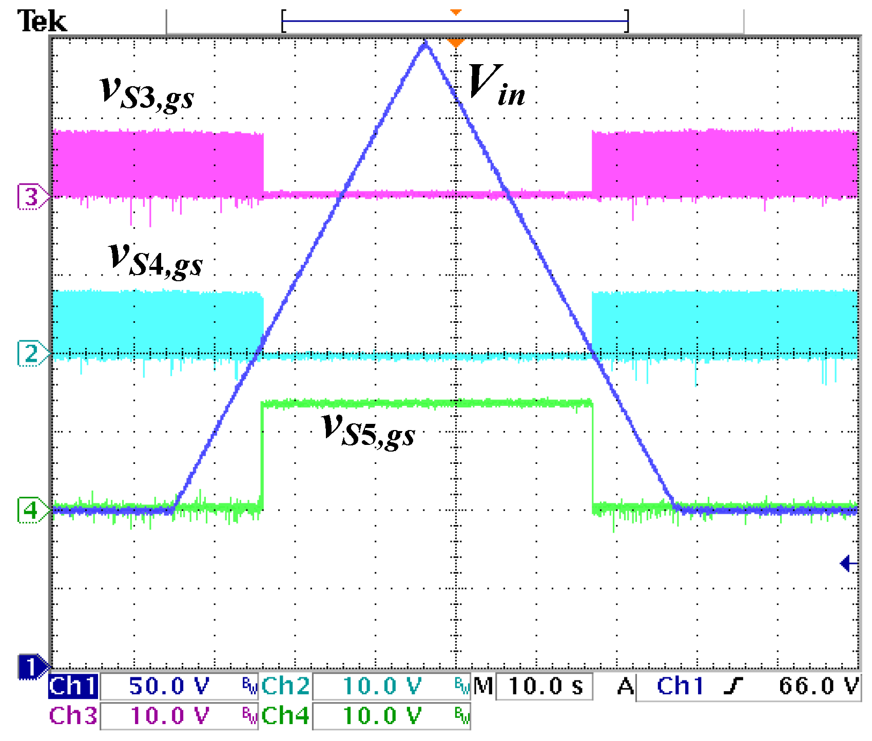
5. Prototype and Experimental Results
6. Conclusions
Funding
Acknowledgments
Conflicts of Interest
References
- Guerrero, J.M.; Loh, P.C.; Lee, T.L.; Chandorkar, M. Advanced control architectures for intelligent microgrids—Part II: Power quality, energy storage, and ac/dc microgrids. IEEE Trans. Ind. Electron. 2013, 60, 1263–1270. [Google Scholar] [CrossRef] [Green Version]
- Meng, L.; Shafiee, Q.; Trecate, G.F.; Karimi, H.; Fulwani, D.; Lu, X.; Guerrero, J.M. Review on control of DC microgrids and multiple microgrid clusters. IEEE J. Emerg. Sel. Top. Power Electron. 2017, 5, 928–948. [Google Scholar]
- Jing, W.; Lai, C.H.; Wong, S.H.W.; Wong, M.L.D. Battery-super capacitor hybrid energy storage system in standalone dc microgrids: A review. IET Renew. Power Gener. 2017, 11, 461–469. [Google Scholar] [CrossRef]
- Emadi, A.; Lee, Y.J.; Rajashekara, K. Power electronics and motor drives in electric, hybrid electric, and plug-in hybrid electric vehicles. IEEE Trans. Ind. Electron. 2008, 55, 2237–2245. [Google Scholar] [CrossRef]
- Mangu, B.; Akshatha, S.; Suryanarayana, D.; Fernandes, B.G. Grid-connected PV-wind-battery-based multi-input transformer-couple bidirectional dc-dc converter for household applications. IEEE J. Emerg. Sel. Top. Power Electron. 2016, 4, 1086–1095. [Google Scholar] [CrossRef]
- Yilmaz, M.; Krein, P.T. Review of battery charger topologies, charging power levels, and infrastructure for plug-in electric and hybrid vehicles. IEEE Trans. Power Electron. 2013, 28, 2151–2169. [Google Scholar] [CrossRef]
- Ahrabi, R.R.; Ardi, H.; Elmi, M.; Ajami, A. A novel step-up multi input dc-dc converter for hybrid electric vehicles application. IEEE Trans. Power Electron. 2017, 32, 3549–3561. [Google Scholar] [CrossRef]
- Xu, D.; Zhao, C.; Fan, H. A PWM plus phase-shift control bidirectional DC-DC converter. IEEE Trans. Power Electron. 2004, 19, 666–675. [Google Scholar] [CrossRef]
- Lara, J.; Masisi, L.; Hernandez, C.; Arjona, A.; Chandra, A. Novel five-level ANPC bidirectional converter for power quality enhancement during G2V/V2G operation of cascaded EV charger. Energies 2021, 14, 2650. [Google Scholar] [CrossRef]
- Rico, S.J.; Pagano, D.J.; Lucas, K.E. Bidirectional power sharing for DC microgrid enabled by dual active bridge DC-DC converter. Energies 2021, 14, 404. [Google Scholar]
- Jain, A.K.; Ayyanar, R. PWM control of dual active bridge: Comprehensive analysis and experimental verification. IEEE Trans. Power Electron. 2011, 26, 1215–1227. [Google Scholar] [CrossRef]
- Zou, S.; Lu, J.; Mallik, A.; Khaligh, A. Bi-directional CLLC converter with synchronous rectification for plug-in electric vehicles. IEEE Trans. Ind. Appl. 2018, 54, 998–1005. [Google Scholar] [CrossRef]
- Jung, J.H.; Kim, H.S.; Ryu, M.H.; Baek, J.W. Design methodology of bidirectional CLLC resonant converter for high-frequency isolation of DC distribution systems. IEEE Trans. Power Electron. 2013, 28, 1741–1755. [Google Scholar] [CrossRef]
- Liu, Y.; Du, G.; Wang, X.; Lei, Y. Analysis and design of high-efficiency bidirectional GaN-based CLLC resonant converter. Energies 2019, 12, 3859. [Google Scholar] [CrossRef] [Green Version]


| Topology | Power Switches | Split dc Capacitor | Resonant Components | Voltage Range, Power Rating |
|---|---|---|---|---|
| Proposed converter | 10 | 2 | 4 | Vin = 100–400 V, Vo = 48 V, Po = 1 kW |
| Half bridge CLLC converter | 4 | 4 | 4 | Vin = 400–600 V, Vo = 300–450 V, Po = 3.3 kW in [13] |
| Full bridge CLLC converter | 8 | 0 | 4 | Vin = 382–408 V, Vo = 50 V, Po = 400 W in [12] |
| Dual active bridge converter | 8 | 0 | 1 | Vin = 600 V, Vo = 300–450 V, Po = 10 kW in [12] |
| Items | Parameter |
|---|---|
| Primary side split capacitances C1, C2 | 220 μF/400 V |
| Primary side resonant capacitance Cr,p | 265 nF |
| Primary side resonant inductance Lr,p | 9.5 μH |
| Primary side magnetizing inductance Lm,p | 47.5 μH |
| Primary side switches S1–S5 | GP50B60PD1 (600 V/33 A) |
| Secondary side resonant capacitance Cr,s | 4.24 μF |
| Secondary side resonant inductance Lr,s | 0.6 μH |
| Secondary side switches Q1–Q4 | IPP05CN10N G (100 V/100 A) |
| Secondary output capacitance Co | 3000 μH/100 V |
| Transformer np:ns | 24:6 (PC40 EER42) |
Publisher’s Note: MDPI stays neutral with regard to jurisdictional claims in published maps and institutional affiliations. |
© 2021 by the author. Licensee MDPI, Basel, Switzerland. This article is an open access article distributed under the terms and conditions of the Creative Commons Attribution (CC BY) license (https://creativecommons.org/licenses/by/4.0/).
Share and Cite
Lin, B.-R. Implementation of a Resonant Converter with Topology Morphing to Achieve Bidirectional Power Flow. Energies 2021, 14, 5186. https://doi.org/10.3390/en14165186
Lin B-R. Implementation of a Resonant Converter with Topology Morphing to Achieve Bidirectional Power Flow. Energies. 2021; 14(16):5186. https://doi.org/10.3390/en14165186
Chicago/Turabian StyleLin, Bor-Ren. 2021. "Implementation of a Resonant Converter with Topology Morphing to Achieve Bidirectional Power Flow" Energies 14, no. 16: 5186. https://doi.org/10.3390/en14165186
APA StyleLin, B.-R. (2021). Implementation of a Resonant Converter with Topology Morphing to Achieve Bidirectional Power Flow. Energies, 14(16), 5186. https://doi.org/10.3390/en14165186