Article

High-Gain High-Efficiency DC–DC Converter with Single-Core Parallel Operation Switched Inductors and Rectifier Voltage Multiplier Cell

by
Eduardo Augusto Oliveira Barbosa
,
Márcio Rodrigo Santos de Carvalho
,
Leonardo Rodrigues Limongi
,
Marcelo Cabral Cavalcanti
*,
Eduardo José Barbosa
and
Gustavo Medeiros de Souza Azevedo
Department of Electrical Engineering, Federal University of Pernambuco, Recife 50740-550, Brazil
*
Author to whom correspondence should be addressed.
Energies 2021, 14(15), 4634; https://doi.org/10.3390/en14154634
Submission received: 2 July 2021 / Revised: 22 July 2021 / Accepted: 23 July 2021 / Published: 30 July 2021
(This article belongs to the Section F: Electrical Engineering)

Abstract

:
This paper proposes a high step-up high-efficiency converter, comprised of an active switched coupled-inductor cell. The secondary windings are integrated into a rectifier voltage multiplier cell in a boost-flyback configuration, allowing the operation with high voltage gain with low switches duty cycle and low turn-ratios on the coupled-inductors. Both coupled-inductors are integrated into a single core due to the parallel operation of the switches. The leakage inductances of the coupled-inductors are used to mitigate the reverse recovery currents of the diodes, while regenerative clamp circuits are used to protect the switches from the voltage spikes caused by the leakage inductances. The operation of the converter is analyzed both quantitatively and qualitatively, and the achieved results are validated through experimentation of a 400 W prototype. A 97.1% CEC efficiency is also reported.

1. Introduction

Currently, many applications require DC–DC low voltage (20–50 V) to high voltage (380–400 V) power conversion. In the context of sustainable energy generation, solar photovoltaic (PV) and fuel-cell (FC) are attractive alternative power sources in which power is generated at low voltage [1,2,3,4]. In electrical and hybrid vehicles, high voltage step-up is needed to convert the low voltage from the battery bank, FC or supercapacitors to the high voltage level required by the electric motors [5,6,7]. Other possible applications of high voltage converters are uninterruptible power supplies (UPS), high voltage light emitting diodes (LEDs), high intensity discharge (HID) lamps for vehicular headlights, among others [8,9,10,11].
The ideal boost converter can provide a high static voltage gain by operating with duty cycle near the unit. However, this generates elevated voltage stress on the semiconductor elements of the converter—which demands the use of high on-resistance semiconductors—and increases the reverse recovery current in the diodes resulting in higher losses. Moreover, the increased losses affect the static gain of the converter, resulting in decreased output voltage [12,13].
Many Switched-Inductor cell (SL)-based DC–DC converters have been proposed in the literature to achieve high voltage gain. In [2,9,14], DC–DC converters with high voltage gain were obtained by employing passive SL cells comprised of only diodes and inductors. However, this causes the main switches to suffer from high voltage stress, which demands the use of high on-resistance semiconductors. In [15,16], the Active Switched-Inductor cell (A-SL) is used, replacing the diodes with the dual active switches, which results in reduction of conduction losses due to decreased voltage stress. Moreover, as the switches are in parallel, the current on each switch is halved, decreasing the losses. The A-SL cell can employ P-SL cells along with magnetic coupling techniques [15,16,17,18] to further increase the static voltage gain by using coupled-inductors with proper turn-ratios, without operating at extreme duty cycle values. In addition, by using high frequency switching, it is possible to employ compact magnetic cores and reduce the converter total weight and volume, making the use of magnetic coupling very attractive [1,3,4,5,11,15,16,17,18,19,20,21,22,23,24,25,26,27]. Furthermore, the magnetic element leakage inductance [28] can be used to mitigate the recovery current of the diodes.
DC–DC converters based on Voltage Multiplier Cells (VMCs)—which are arrangements of semiconductors, capacitors and inductors generally introduced after the main switch—are able to provide high voltage gain with low component count. VMCs are modular and can be cascaded or combined with other VMCs in order to improve voltage gain, add positive traits or mitigate negative characteristics of other voltage gain enhancing techniques. To further improve the voltage gain, coupled-inductors and built-in transformers can be employed simultaneously with or integrated to the VMCs [22,23,24,25,26,29,30]. This versatility, which allows combining the positive characteristics of different voltage lifting techniques, in addition to simple structures and ease of integration to any converter allows the use of VMCs in DC–DC converters for a multitude of applications.
Interleaved DC–DC converters are capable to achieve high voltage gain and present the beneficial features of reduced current ripples and current stress on the switches, due to the input current sharing between phases, while still maintaining good power density [25,26,27]. This arrangement, however, leads to an increased number of components with the same power rating of a single switch converter, as each phase of the interleaved converter operates alternately to each other.
To overcome the aforementioned disadvantages, this paper proposes a new high step-up, high efficiency VMC coupled switched-inductors based DC–DC converter. The coupled-inductors primary windings are inside an A-SL cell and the secondary windings are placed in series as the input of a rectifier VMC. The VMC output capacitors are placed in a boost-flyback configuration, which permits high voltage gain with small voltage stress across all components, allowing the use of low R d s , o n semiconductors. Since both pairs of windings share the same operation modes, the magnetic components are integrated into a single core. Furthermore, the coupled-inductors leakage inductances are used to mitigate the diodes reverse current, further reducing conduction losses. To supress voltage spikes on the switches, regenerative clamper circuits are used.

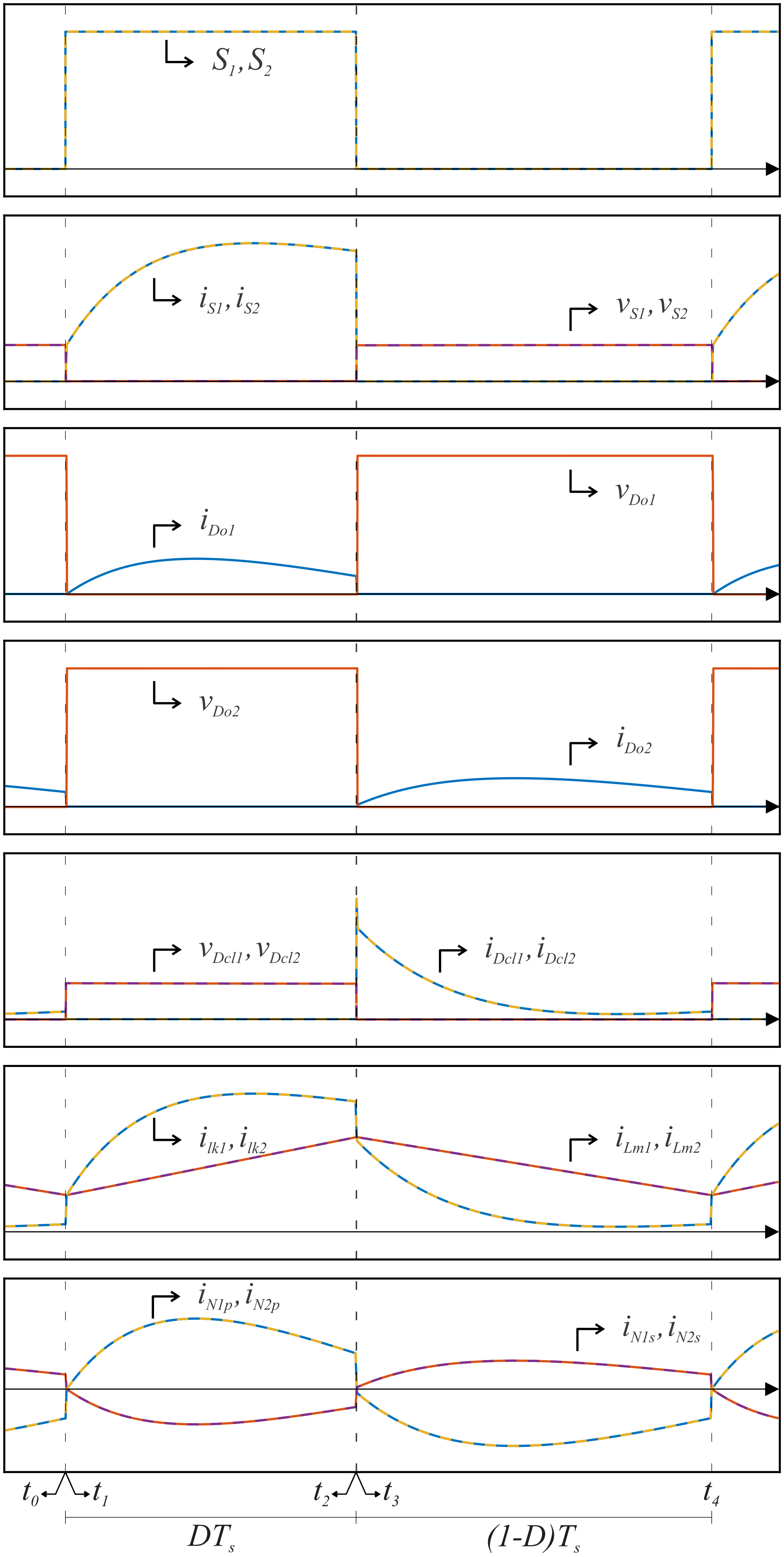
2. Proposed Converter Topology and Operation Analysis

The proposed converter is shown in Figure 1 and its main waveforms are shown in Figure 2, where:
  • N p 1 , N s 1 , N p 2 and N s 2 are, respectively, the number of turns of the primary and the secondary windings of the first and the second coupled-inductor, where N s 1 N p 1 = N s 2 N p 2 = n ;
  • r w 1 , r w 2 are the resistances on the windings of the first and the second coupled-inductor, respectively;
  • l l k 1 , l l k 2 are the leakage inductances of the first and the second coupled-inductor, respectively;
  • L m 1 and L m 2 are the magnetizing inductances of the first and the second coupled-inductor, respectively;
  • S 1 and S 2 are the switches;
  • D o 1 and D o 2 are the output diodes;
  • D c l 1 and D c l 2 are the clamper circuit diodes;
  • C o 1 , C o 2 and C o 3 are the output capacitors;
  • C c l 1 and C c l 2 are the clamper circuit capacitors;
  • C i n is the input capacitor.
Moreover, the converter operates at switching frequency f s and duty cycle D. The converter main operation states for the continuous conduction mode (CCM) are shown in Figure 3 and described as follows:

2.1. State I [ t 0 t 1 ]

At t 0 , switches S 1 and S 2 are turned on. The leakage inductances, l l k 1 and l l k 2 , are charged by capacitors C i n and C o 2 , while the magnetizing inductances, L m 1 and L m 2 , are discharged with voltage V C o 2 2 n . The difference between the currents on l l k 1 and l l k 2 and the current on L m 1 and L m 2 , respectively, flows through the primary windings of the coupled-inductors and through diode D o 2 , decaying until it reaches zero. All the remaining diodes are reverse biased. This state ends when the leakage currents, i l k 1 and i l k 2 , become equal in value to the magnetizing currents, i L m 1 and i L m 2 . Although there is a formation of a resonant circuit between the leakage inductances, C i n and C o 2 , this state is very brief as can be noted from Figure 2 and the currents on the components can be represented by a linear approximation as
i L m 1 ( t ) = V C o 2 2 n L m 1 ( t t 0 ) + i L m 1 ( t 0 ) ,
i l k 1 ( t ) = i S 1 ( t ) = V C o 2 2 n + V i n l l k 1 ( t t 0 ) + i L k 1 ( t 0 ) ,
i D o 2 ( t ) = V i n n l l k 1 + V C o 2 2 n 2 1 L m 1 + 1 l l k 1 ( t t 0 ) + i L m 1 ( t 0 ) n i L k 1 ( t 0 ) n .
Due to the circuit symmetry, all equations pertaining to the first pair of windings are also valid for the second pair of windings. The equivalent circuit of the converter during this state is shown in Figure 3a.

2.2. State II [ t 1 t 2 ]

Currents i l k 1 and i l k 2 values surpass i L m 1 and i L m 2 at instant t 1 , shown in Figure 3b. This causes the currents in both primary windings to change direction, which subsequently causes diode D o 1 to be forward biased and capacitor C o 1 to charge, while D o 2 becomes reverse biased. Due to D o 1 being forward biased, C o 1 is now in parallel with the secondary windings of the coupled-inductor, making L m 1 and L m 2 to be charged with voltage V C o 1 2 n and, consequently, l l k 1 and l l k 2 are charged with voltage V i n V C o 1 2 n . A resonant circuit is formed between i l k 1 , i l k 2 , C i n and C o 1 , leading to the appearance of high frequency sinusoidal currents in these components and semiconductors. This state ends when S 1 and S 2 are commanded to turn off. This state can be described by the following Equations:
i L m 1 ( t ) = V C o 1 2 n L m 1 ( t t 1 ) + i L m 1 ( t 1 ) ,
i l k 1 ( t ) = i S 1 ( t ) = V i n V C o 1 2 n r w 1 2 + ( ω d , I I l l k 1 ) 2 e α I I ( t t 1 ) sin ω d , I I ( t t 1 ) + V C o 1 2 n L m 1 ( t t 1 ) + i L m 1 ( t 1 ) ,
i D o 1 ( t ) = V i n V C o 1 2 n n r w 1 2 + ( ω d , I I l l k 1 ) 2 e α I I ( t t 1 ) sin ω d , I I ( t t 1 ) ,
where the equivalent elements regarding the resonant circuit during this state are:
R e q I I = r w 1 ,
L e q I I = l l k 1 ,
C e q I I = 2 n 2 C i n C o 1 C i n + 4 n 2 C o 1 .
Furthermore, the attenuation of the resonant circuit α I I is given by
α e q I I = r e q I I 2 L e q I I ,
and the resonant frequency of the circuit is
ω d , I I = 1 L e q I I C e q I I α I I 2 .
The equivalent circuit of the converter during this state can be seen in Figure 3b.

2.3. State III [ t 2 t 3 ]

At t 2 , both switches are turned off. Diodes D c l 1 and D c l 2 become forward biased and capacitors C c l 1 , C c l 2 and C o 3 start to be charged. This causes l l k 1 and l l k 2 to start discharging with voltage V i n V C o 1 2 n V C c l 1 , consequently leading their currents to decay. The diminishing currents on the leakage inductances cause the currents on the windings of the coupled-inductors and D o 1 to decay as well. This stage ends when i l k 1 and i l k 2 become equal to i L m 1 and i L m 2 . Similarly to State I, there is the formation of a resonant circuit between the leakage inductances, C i n , C o 1 and C o 3 , but this state is very brief and the currents on these components and the semiconductors can be represented by linear approximations. Throughout this state, Equation (4) is still valid, while the leakage inductances and diode D o 1 currents are given by:
i l k 1 ( t ) = i D c l 1 ( t ) = V i n V C o 1 2 n V C c l 1 l l k 1 ( t t 2 ) + i l k 1 ( t 2 ) ,
i D o 1 ( t ) = V i n V C c l 1 n l l k 1 V C o 1 2 n 2 1 L m 1 + 1 l l k 1 ( t t 2 ) i L m 1 ( t 2 ) + i L k 1 ( t 2 ) .
The converter equivalent circuit during this state is shown in Figure 3c

2.4. State IV [ t 3 t 4 ]

Currents i l k 1 and i l k 2 values become smaller than i m 1 and i L m 2 at t 3 , which change the primary winding currents direction once more. This results in D o 1 being reverse biased and D o 2 to be forward biased. Consequently, C o 2 is now in parallel with the secondary windings of the coupled-inductor, leading to L m 1 and L m 2 to be discharged with voltage V C o 2 2 n , while l l k 1 and l l k 2 are discharged with voltage V i n + V C o 2 2 n V c c l 1 . A resonant circuit is formed between l l k 1 , l l k 2 , C i n , C o 2 and C o 3 , leading to the appearance of high frequency sinusoidal currents in these components and semiconductors. This state ends when S 1 and S 2 are commanded to turn on at t 4 , restarting the cycle. The following equations can be used to describe this state:
i L m 1 ( t ) = V C o 2 2 n L m 1 ( t t 3 ) + i L m 1 ( t 3 ) ,
i l k 1 ( t ) = i D c l 1 ( t ) = V i n + V C o 2 2 n V C c l 1 r w 1 2 + ( ω d , I V l l k 1 ) 2 e α I V ( t t 3 ) sin ω d , I V ( t t 3 ) V C o 2 2 n L m 1 ( t t 3 ) + i L m 1 ( t 3 ) ,
i D o 2 ( t ) = V i n + V C o 2 2 n V C c l 1 n r w 1 2 + ( ω d , I V l l k 1 ) 2 e α I V ( t t 3 ) sin ω d , I V ( t t 3 ) .
where
R e q I V = r w 1 + r w 2 ,
L e q I V = l l k 1 + l l k 2 ,
C e q I V = n 2 C i n C o 2 C o 3 C i n + n 2 C o 2 + C o 3 ,
α e q I V = r e q I V 2 L e q I V ,
ω d , I V = 1 L e q I V C e q I V α I V 2 .
The converter equivalent circuit during this State can be seen in Figure 3d.

3. Proposed Converter Steady-State Analysis

In order to facilitate the steady-state analysis of the proposed converter, the following assumptions are made:
  • All components are ideal;
  • The magnetizing inductances have the same value;
  • N s 1 N p 1 = N s 2 N p 2 = n ;
  • The voltages across the capacitors are constant.
Since the leakage inductances influence is not represented, States I and III are not taken into consideration in the analyses made in this section, as these states are mainly characterized by the charge and discharge, respectively, of these inductances.

3.1. Voltage Stresses on the Capacitors

From Figure 3b, C i n is in parallel to the magnetizing inductances and the primary windings during State II, while C o 1 is in parallel to the secondary windings, resulting in
V C o 1 = 2 n V i n .
By applying the volt-second balance principle to the magnetizing inductances, it can be seen that during State IV
V C o 2 = 2 n D 1 D V i n .
Moreover, applying the Kirchhoff’s Voltage Law (KVL) to the lower loop of the circuit during State IV results in
V C o 3 = 1 + D 1 D V i n
The voltage across the clamper capacitors C c l 1 and C c l 2 can be found applying the KVL during State IV
V C c l 1 = V C c l 2 = 1 1 D V i n ,

3.2. Voltage Stresses on the Semiconductors

Since C c l 1 and C c l 2 are connected in parallel to S 1 and S 2 , respectively, during State IV, the voltage stress across the switches is given by Equation (25):
V S 1 = V S 2 = 1 ( 1 D ) V i n .
The output diodes D o 1 and D o 2 are subject to the sum of C o 1 and C o 2 voltages during States IV and II, respectively. Therefore, applying the KVL and using Equations (22) and (23) results in
V D o 1 = V D o 2 = 2 n ( 1 D ) V i n .
The clamper diodes D c l 1 and D c l 2 voltage stress can be obtained by applying the KVL during State II and using (25)
V D c l 1 = V D c l 2 = 1 ( 1 D ) V i n .

3.3. Voltage Gain

As can be seen from Figure 1, the output voltage V o is given by the sum of the output capacitors voltages
V o = V C o 1 + V C o 2 + V C o 3 .
The voltage gain G can be found by substituting Equations (22)–(24) into Equation (29), resulting in:
G = 1 + 2 n + D 1 D .
Figure 4 shows the static gain versus duty cycle curves for different turn ratio values. As can be seen, it is possible to achieve very high static gain without need for high duty cycle values.

3.4. Average Current Stresses

The average current through the magnetizing inductances and semiconductors in a switching cycle can be found by applying the ampere-second balance to the capacitors in Figure 1, resulting in
I ¯ L m 1 = I ¯ L m 2 = I i n + I o 2 = ( G + 1 ) 2 I o ,
I ¯ D o 1 = I ¯ D o 2 = I ¯ D c l 1 = I ¯ D c l 2 = I o ,
I ¯ S 1 = I ¯ S 2 = I i n I o 2 = ( G 1 ) 2 I o ,

3.5. Maximum Current Stresses

The maximum current on the magnetizing inductances is equal to its average value plus half of the total ripple. Therefore, utilizing Equations (4), (22) and (31) results in
I ^ L m 1 = I ^ L m 2 = ( G + 1 ) 2 + R D 2 G L m f s I o .
From Figure 2 and (14), the peak current on the clamper diodes occurs at t 3 and is equal to the magnetizing current at the same moment
I ^ D c l 1 = I ^ D c l 2 = ( G + 1 ) 2 + R D 2 G L m f s I o .
The maximum current on the diodes D o 1 and D o 2 can be found by not taking the attenuation during States II and IV into consideration. Since the average current on the output diodes is equal to the average output current (32), it means that
1 T s 0 D T s I ^ D o 1 sin ω d , I I t d t = I o ,
1 T s 0 ( 1 D ) T s I ^ D o 2 sin ω d , I V t d t = I o ,
where T s = 1 f s is the switching period. Thus, solving for the peak currents nets
I ^ D o 1 ω d , I I T s 1 cos ( ω d , I I D T s ) I o ,
I ^ D o 2 ω d , I V T s 1 cos ( ω d , I V ( 1 D ) T s ) I o .
The maximum value of the currents on the switches is difficult to obtain from (4) due to the need to solve a transcendental equation. However, it is easy to note that the maximum value is lesser or equal than the sum of the maximum linear and sinusoidal parts of the equation. As such, by disregarding, it is possible to state that:
I ^ S 1 = I ^ S 2 I ^ L m 1 + n I ^ D o 1 .
Substituting Equations (34) and (38) into Equation (41) results in
I ^ S 1 = I ^ S 2 ( G + 1 ) 2 + R D 2 G L m f s + n ω d , I I T s 1 cos ( ω d , I I D T s ) I o .

4. Performance Comparison

Table 1 shows the performance comparison between the proposed converter and some recently published topologies using some relevant metrics, such as number of total used switches, diodes, capacitors and magnetic cores, the voltage stress on the semiconductors and maximum efficiency. All of the compared converters are non-isolated, high-gain, high-efficiency topologies with similar nominal power rating, employing magnetic coupling, a low number of components and employ two switches.
The converters presented in [16,17] utilize the A-SL cell, substituting the normal inductors for coupled-inductors pairs to increase the voltage gain. Both topologies are very simple, employing a very low quantity of components. Since in both converters the coupled-inductors pairs are switched simultaneously, only one magnetic core is used. The low component count results in high voltage stress and the lack of an input filter results in very high current ripple in the input, which is detrimental to the lifespan of PV modules and fuel cells. Both converters also present low voltage gain when compared to most of the other converters shown.
In [18], a coupled-inductor A-SL converter is also proposed. This converter also employs a rectifier VMC in a boost-flyback configuration, which greatly improve the voltage gain of the converter when compared to [16,17], with the addition of only a few more components. This converter, however, employs two magnetic cores, increasing its volume and weight, and also presents very high input current ripple. Although the voltage stress on the switches and diodes is low, it presents comparatively low efficiency.
The converter proposed in [21] also has very low overall count of elements, using only one magnetic core, two diodes and three capacitors. However, it has one of the lowest voltage gains of all compared converters, which translates into higher voltage stresses on the semiconductor elements. Its voltage gain can be increased by changing the turn-ratio of the coupled-inductor or by cascading the used VMC, which, in turn, decreases the efficiency due to heightened conduction losses. Its maximum reported efficiency is also the lowest from all of the compared converters.
The converter presented in [22] uses its second switch in an active clamper circuit to achieve load-independent soft-switching. The converter voltage gain is low, however, and the voltage stresses between the diodes are not optimally distributed, resulting in several diodes presenting a maximum voltage equal to the output. The converter also presents two magnetic cores due to the interleaved nature of the switches operation. This converter presents high efficiency throughout the entire possible output power interval.
In [24], a soft switching boost-flyback converter with a rectifier VMC is presented. It presents a high voltage gain and efficiency, due to the use of the capacitors of the rectifier VMC and leakage inductances as resonant tanks, allowing for lossless turn-off of the diodes. Furthermore, the voltage stress on the semiconductor components are low and well-distributed. The ausence of a input filter allows for bidirectional currents in the input, which can be harmful to the input source.
An interleaved converter is presented in [26]. This converter features the highest voltage gain and the highest reported efficiency of all compared converters, while also presenting good voltage stress distribution between its semiconductor elements. However, this efficiency was reported at a low output power relative (10%) to the rated power of the converter. Moreover, it also features the highest number of components of all the presented converters.
The presented converter, therefore, shows promise as it achieves high voltage gain using low turn-ratios and duty cycles. It also employs an average number of components, whose voltage stresses are well distributed between them. The simultaneous operation of the switches permits the use of only one magnetic core and also decreases conduction losses due to the shared processing of power between them. Compared to [24], the proposed converter uses less diodes, and the added capacitor removes the high input current ripple, while maintaining the positive characteristics. This results in a high efficiency through all possible operation points.

5. Design Considerations

5.1. Semiconductors Design

The semiconductors can be chosen using Equations (26)–(28) for the maximum rated voltage, Equations (32) and (33) for the average current stress and Equations (35), (38), (39) and (41) for the peak current stress.

5.2. Coupled-Inductor Design

The turn-ratios can be chosen after the range of the duty cycle and the gain are set via
n = G ( 1 D ) 2 ( 1 + D ) .
However, as can be seen from Equations (35) and (41), the maximum current value on the clamper diodes and switches and, therefore, the RMS values of said currents increase along with the turn-ratios. Hence, using excessively high turn-ratios lead to high conduction losses and should be avoided.
The coupled-inductor magnetizing inductance is designed to have a current ripple, relatively to the average current, within the desired limits. The magnetizing currents ripple Δ I L m 1 and Δ I L m 2 are given by
Δ I L m 1 = Δ I L m 2 = 2 I ^ L m 1 I ¯ L m 1 .
Substituting Equations (31) and (34) into Equation (43) results in
Δ I L m 1 = Δ I L m 2 = V i n D L m 1 f s ,
To operate in the CCM, it is necessary that
I ¯ L m 1 Δ I L m 1 2 > 0 .
Substituting Equations (31) and (44) into Equation (45) results in
L m 1 = L m 2 > D R 2 G ( G 1 ) f s .

5.3. Capacitor Design

The voltage rating of the capacitors can be chosen from Equations (22)–(25). The capacitance values of the output capacitors are designed to limit the voltage ripple within the desired thresholds. During State IV, the output capacitor C o 1 discharges into the load with current I o . Thus, its charge variation during State IV can be given by
V C o 1 Δ V C o 1 = ( 1 D ) I o f s .
Substituting Equations (22) and (30) into Equation (47) yields:
C o 1 = ( 1 + D + 2 n ) 2 n R f s Δ V C o 1 / V C o 1 .
Similarly, output capacitors C o 2 and C o 3 discharge into the load during State II with current I o ; therefore:
Δ V C o 2 C o 2 = Δ V C o 3 C o 3 = D I o f s .
By substituting Equations (23) and (30) into Equation (49) it is possible to find
C o 2 = ( 1 + D + 2 n ) 2 n R f s Δ V C o 2 / V C o 2 ,
and substituting Equations (24) and (30) into Equation (49) results in
Δ V C o 3 = ( 1 + D + 2 n ) 2 n R f s Δ V C o 2 / V C o 2 .
The charge variation in the input capacitor C i n during State IV is equal to the sum of the charge variation in C o 2 reflected to the primary windings and C o 3 , resulting in
C i n Δ V i n = ( 2 n ( 1 D ) + 1 ) I o f s ,
and with some manipulations, it is possible to find that
C i n = ( 2 n ( 1 D ) + 1 ) G R f s ( Δ V i n / V i n ) .
It must be noted that all the previously designed capacitors compose the resonant circuits in States II or IV and their capacitance values impact the resonance frequency. As such, it is important to reach a compromise between the need for low voltage ripple in the capacitors with the high frequency resonant currents which can reduce switching losses.
The clamping capacitors need to be large enough to absorb the energy stored in the leakage inductances after the switches are opened and are given by
C c l 1 = C c l 2 = 1 + D π f s 2 1 l l k 1 + l l k 2 .

6. Experimental Results

A prototype with rated power of 400 W was created and tested in order to validate the theoretical analyses performed previously. The experimental prototype is shown in Figure 5 and its design parameters and components are shown in Table 2.
All waveforms measurements were performed using Yokogawa’s DL850 Oscilloscope. The switches gate signals, input voltage and output voltage are shown in Figure 6. It can be seen that the converter is capable of high voltage gain, above ten times, while maintaining low duty cycle, around 0.45, in accordance to Equation (30)
The currents and drain-source voltages waveforms on both switches are shown in Figure 7. The voltage stress on the switches are much smaller than the output voltage, around 70 V, validating Equation (26). This makes possible employing low-voltage rating and, therefore, low R D S , o n switches, decreasing the conduction losses.
From the output diodes waveforms, shown in Figure 8, it is possible to observe that the voltage stresses are lower than the output voltage. This, combined with the decaying currents, results in decreased switching losses. The use of ultrafast recovery diodes in the circuit causes the fast rise of current on the moment these diodes are forward biased, due to the forward recovery effect.
Similarly, from the clamper diodes waveforms, shown in Figure 9, it can be seen that the voltage stresses are as low as the voltage stresses on the switches, with reduced switching losses due to the naturally decaying current waveforms.
Finally, the currents on the magnetic components are shown in Figure 10. The magnetizing current shows that the converter is currently operating in the continuous conduction mode, while the leakage current shows the naturally decaying current waveform, which evidentiates the leakage inductances role in mitigating the diodes switching losses.
The efficiency of the proposed converter was measured using Yokogawa’s WT1800 power analyzer in two different tests. In the first test, the converter is submitted to resistive loads of different power under a constant output voltage and duty cycle. In the second test, the load power and output voltage are constant while the duty cycle is changed. From the efficiency results, shown in Figure 11, the CEC efficiency is given by
η C E C = 0.04 η 10 % + 0.05 η 20 % + 0.12 η 30 % + 0.21 η 50 % + 0.53 η 75 % + 0.05 η 100 % = 97.12 % .
where η X % indicates the efficiency at X % of the nominal rated power.

7. Conclusions

A new high-gain, high-efficiency converter utilizing active switched coupled-inductors and rectifier VMC techniques was proposed. By combining the AS-L cell with rectifier VMC techniques, the proposed converter is capable of achieving high voltage gain without high duty cycle and turn-ratios and low total component count. The use of coupled-inductor reduces the voltage stress on the switches, which enable the use of low R d s , o n switches, decreasing losses. Furthermore, since the switches are switched simultaneously, the current through each switch is halved. This also permits the integration of both coupled-inductors into a single-core, reducing volume and weight. The coupled-inductors leakage inductances are utilized to reduce the reverse-recovery current losses, and their energy are recycled through the use of regenerative clamper circuits. A 400 W prototype was tested, validating the previously performed analyses and achieving high efficiency.

Author Contributions

Analysis and Design, E.A.O.B.; Experiment, E.A.O.B., M.R.S.d.C. and E.J.B.; Writing, E.A.O.B., M.R.S.d.C. and E.J.B.; Review and Editing, L.R.L., G.M.d.S.A. and M.C.C.; Supervision, L.R.L.; Funding acquisition, L.R.L., G.M.d.S.A. and M.C.C. All authors have read and agreed to the published version of the manuscript.

Funding

This research was partially supported by Coordenação de Aperfeiçoamento de Pessoal de Nível Superior—CAPES, Conselho Nacional de Desenvolvimento Cientifico e Tecnologico—CNPq Grant No. 305901/2015-0 and 306304/2018-0 and Fundacao de Amparo a Ciencia e Tecnologia do Estado de Pernambuco—Facepe Grant No. APQ-0777-3.04/14.

Institutional Review Board Statement

Not applicable.

Informed Consent Statement

Not applicable.

Data Availability Statement

Not applicable.

Conflicts of Interest

The authors declare no conflict of interest.

References

  1. Chang, L.-Y.; Chang, J.-H.; Chao, K.-H.; Chung, Y.-N. A Low-Cost High-Performance Interleaved Inductor-Coupled Boost Converter for Fuel Cells. Energies 2016, 9, 792. [Google Scholar] [CrossRef] [Green Version]
  2. Ahmad, J.; Zaid, M.; Sarwar, A.; Lin, C.-H.; Asim, M.; Yadav, R.K.; Tariq, M.; Satpathi, K.; Alamri, B. A New High-Gain DC-DC Converter with Continuous Input Current for DC Microgrid Applications. Energies 2021, 14, 2629. [Google Scholar] [CrossRef]
  3. Sayed, K.; Gronfula, M.G.; Ziedan, H.A. Novel Soft-Switching Integrated Boost DC-DC Converter for PV Power System. Energies 2020, 13, 749. [Google Scholar] [CrossRef] [Green Version]
  4. Gu, B.; Dominic, J.; Chen, B.; Zhang, L.; Lai, J. Hybrid Transformer ZVS/ZCS DC–DC Converter with Optimized Magnetics and Improved Power Devices Utilization for Photovoltaic Module Applications. IEEE Trans. Power Electron. 2015, 30, 2127–2136. [Google Scholar] [CrossRef]
  5. Yan, F.; Li, J.; Du, C.; Zhao, C.; Zhang, W. A Coupled-Inductor DC-DC Converter with Input Current Ripple Minimization for Fuel Cell Vehicles. Energies 2019, 12, 1689. [Google Scholar] [CrossRef] [Green Version]
  6. Bi, H.; Wang, P.; Che, Y. A Capacitor Clamped H-Type Boost DC-DC Converter with Wide Voltage-Gain Range for Fuel Cell Vehicles. IEEE Trans. Veh. Technol. 2019, 68, 276–290. [Google Scholar] [CrossRef]
  7. Wu, X.; Yang, M.; Zhou, M.; Zhang, Y.; Fu, J. A Novel High-Gain DC-DC Converter Applied in Fuel Cell Vehicles. IEEE Trans. Veh. Technol. 2020, 69, 12763–12774. [Google Scholar] [CrossRef]
  8. Aamir, M.; Ullah Tareen, W.; Ahmed Kalwar, K.; Ahmed Memon, M.; Mekhilef, S. A High-Frequency Isolated Online Uninterruptible Power Supply (UPS) System with Small Battery Bank for Low Power Applications. Energies 2017, 10, 418. [Google Scholar] [CrossRef] [Green Version]
  9. Marroqui, D.; Garrigós, A.; Torres, C.; Orts, C.; Blanes, J.M.; Gutierrez, R. Interleaved, Switched Inductor and High-Gain Wide Bandgap Based Boost Converter Proposal. Energies 2021, 14, 800. [Google Scholar] [CrossRef]
  10. Forouzesh, M.; Yari, K.; Baghramian, A.; Hasanpour, S. Single-switch high step-up converter based on coupled inductor and switched capacitor techniques with quasi-resonant operation. IET Power Electron. 2017, 10, 240–250. [Google Scholar]
  11. Siwakoti, Y.P.; Blaabjerg, F. Single Switch Nonisolated Ultra-Step-Up DC–DC Converter with an Integrated Coupled Inductor for High Boost Applications. IEEE Trans. Power Electron. 2017, 32, 8544–8558. [Google Scholar] [CrossRef]
  12. Tofoli, F.L.; Pereira, D.D.C.; Josias de Paula, W.; Oliveira Junior, D.D.S. Survey on non-isolated high-voltage step-up dc-dc topologies based on the boost converter. IET Power Electron. 2015, 8, 2044–2057. [Google Scholar] [CrossRef] [Green Version]
  13. Wong, Y.-S.; Chen, J.-F.; Liu, K.-B.; Hsieh, Y.-P. A Novel High Step-Up DC-DC Converter with Coupled Inductor and Switched Clamp Capacitor Techniques for Photovoltaic Systems. Energies 2017, 10, 378. [Google Scholar] [CrossRef] [Green Version]
  14. Axelrod, B.; Berkovich, Y.; Ioinovici, A. Switched-Capacitor/Switched-Inductor Structures for Getting Transformerless Hybrid DC–DC PWM Converters. IEEE Trans. Circuits Syst. 2008, 55, 687–696. [Google Scholar] [CrossRef]
  15. Tang, Y.; Fu, D.; Wang, T.; Xu, Z. Analysis of Active-Network Converter with Coupled Inductors. IEEE Trans. Power Electron. 2015, 30, 4874–4882. [Google Scholar] [CrossRef]
  16. Liu, H.; Li, F. Novel High Step-Up DC–DC Converter with an Active Coupled-Inductor Network for a Sustainable Energy System. IEEE Trans. Power Electron. 2015, 30, 6476–6482. [Google Scholar] [CrossRef]
  17. Liu, H.; Li, F. A Novel High Step-up Converter with a Quasi-active Switched-Inductor Structure for Renewable Energy Systems. IEEE Trans. Power Electron. 2016, 31, 5030–5039. [Google Scholar] [CrossRef]
  18. Cao, Y.; Samavatian, V.; Kaskani, K.; Eshraghi, H. A Novel Nonisolated Ultra-High-Voltage-Gain DC–DC Converter with Low Voltage Stress. IEEE Trans. Ind. Electron. 2017, 64, 2809–2819. [Google Scholar] [CrossRef]
  19. Ai, J.; Lin, M. Ultralarge Gain Step-Up Coupled-Inductor DC–DC Converter with an Asymmetric Voltage Multiplier Network for a Sustainable Energy System. IEEE Trans. Power Electron. 2017, 32, 6896–6903. [Google Scholar] [CrossRef]
  20. Forouzesh, M.; Shen, Y.; Yari, K.; Siwakoti, Y.P.; Blaabjerg, F. High-Efficiency High Step-Up DC–DC Converter with Dual Coupled Inductors for Grid-Connected Photovoltaic Systems. IEEE Trans. Power Electron. 2018, 33, 5967–5982. [Google Scholar] [CrossRef]
  21. Ye, Y.; Cheng, K.W.E.; Chen, S. A High Step-up PWM DC-DC Converter with Coupled-Inductor and Resonant Switched-Capacitor. IEEE Trans. Power Electron. 2017, 32, 7739–7749. [Google Scholar] [CrossRef]
  22. Meier, M.B.; da Silva, S.A.; Badin, A.A.; Romaneli, E.F.R.; Gules, R. Soft-Switching High Static Gain DC–DC Converter without Auxiliary Switches. IEEE Trans. Ind. Electron. 2018, 65, 2335–2345. [Google Scholar] [CrossRef]
  23. Hassan, W.; Lu, D.D.-C.; Xiao, W. Single-Switch High Step-Up DC–DC Converter with Low and Steady Switch Voltage Stress. IEEE Trans. Ind. Electron. 2019, 66, 9326–9338. [Google Scholar] [CrossRef]
  24. Sathyan, S.; Suryawanshi, H.M.; Singh, B.; Chakraborty, C.; Verma, V.; Ballal, M.S. ZVS–ZCS High Voltage Gain Integrated Boost Converter for DC Microgrid. IEEE Trans. Ind. Electron. 2016, 63, 6898–6908. [Google Scholar] [CrossRef]
  25. Nouri, T.; Vosoughi, N.; Hosseini, S.H.; Babaei, E.; Sabahi, M. An Interleaved High Step-Up Converter with Coupled Inductor and Built-In Transformer Voltage Multiplier Cell Techniques. IEEE Trans. Ind. Electron. 2019, 66, 1894–1905. [Google Scholar] [CrossRef]
  26. Chen, S.-J.; Yang, S.-P.; Huang, C.-M.; Chen, Y.-H. Interleaved High Step-Up DC–DC Converter with Voltage-Lift and Voltage-Stack Techniques for Photovoltaic Systems. Energies 2020, 13, 2537. [Google Scholar] [CrossRef]
  27. De Carvalho, M.R.S.; Bradaschia, F.; Rodrigues Limongi, L.; de Souza Azevedo, G.M. Modeling and Control Design of the Symmetrical Interleaved Coupled-Inductor-Based Boost DC-DC Converter with Clamp Circuits. Energies 2019, 12, 3432. [Google Scholar] [CrossRef] [Green Version]
  28. Orosz, T.; Tamus, Z.Á. Non-linear Impact of the Short Circuit Impedance Selection on the Cost Optimized Power Transformer Design. Period. Polytech. Electr. Eng. Comput. Sci. 2020, 64, 221–228. [Google Scholar] [CrossRef] [Green Version]
  29. Alzahrani, A.; Shamsi, P.; Ferdowsi, M. Interleaved Multistage Step-Up Topologies with Voltage Multiplier Cells. Energies 2020, 13, 5990. [Google Scholar] [CrossRef]
  30. Forouzesh, M.; Siwakoti, Y.P.; Gorji, S.A.; Blaabjerg, F.; Lehman, B. Step-Up DC–DC Converters: A Comprehensive Review of Voltage-Boosting Techniques, Topologies, and Applications. IEEE Trans. Power Electron. 2017, 32, 9143–9178. [Google Scholar] [CrossRef]
Figure 1. Equivalent circuit of the proposed converter.
Energies 14 04634 g001
Figure 2. Converter main current and voltage waveforms during a switching cycle.
Energies 14 04634 g002
Figure 3. Topological states of the proposed converter. (a) State I, (b) State II, (c) State III, (d) State IV.
Energies 14 04634 g003
Figure 4. Duty cycle versus voltage gain curves under different turn-ratios.
Energies 14 04634 g004
Figure 5. The assembled 400 W laboratory prototype.
Energies 14 04634 g005
Figure 6. Top: switches gate signals v g s 1 and v g s 2 (5 V/div); bottom: input voltage v i n (20 V/div) and output voltage v o (100 V/div).
Energies 14 04634 g006
Figure 7. Top: switch S 1 voltage v S 1 (20 V/div) and current i s 1 (2 A/div); bottom: switch S 2 voltage v S 2 (20 V/div) and current i s 2 (2 A/div).
Energies 14 04634 g007
Figure 8. Top: diode D o 1 voltage v D o 1 (100 V/div) and current i D o 1 (500 mA/div); bottom: diode D o 2 voltage v D o 2 (100 V/div) and current i D o 2 (500 mA/div).
Energies 14 04634 g008
Figure 9. Top: diode D c l 1 voltage v D c l 1 (20 V/div) and current i D c l 1 (500 mA/div); bottom: diode D c l 2 voltage v D c l 2 (20 V/div) and current i D c l 2 (500 mA/div).
Energies 14 04634 g009
Figure 10. Top: primary winding N 1 p current (2 A/div) and secondary winding N 1 s (2 A/div); bottom: leakage inductance l k 1 current (2 A/div) and magnetizing inductance L m 1 current (2 A/div).
Energies 14 04634 g010
Figure 11. Efficiency tests results: different loads under constant duty cycle and 400 V output voltage, different duty cycle under constant 200 W and 400 V output voltage.
Energies 14 04634 g011
Table 1. Performance comparison between the proposed converter and other recently proposed topologies.
No. of Comp.Voltage GainMax. Voltage StressEfficiency
S D C Cor. Switches Diodes Max. Full Load
Proposed2461 1 + 2 n + D 1 D V o 1 + 2 n + D 2 n V o 1 + 2 n + D 97.3%95.9%
[16]2221 1 + 2 n D + D 1 D V o 1 + 2 n D + D ( 2 n + 1 ) V o 1 + 2 n D + D 95.9%95.1%
[17]2331 1 + 2 n D + D 1 D V o 1 + 2 n D + D 2 n V o 1 + 2 n D + D 96.4%95.2%
[18]2552 3 + 2 n + D 1 D V o 3 + 2 n + D 2 n D V o 3 + 2 n + D 94.0%93.0%
[21]2231 2 + n 1 D V o 2 + n ( n + 1 ) V o 2 + n 93.9%93.3%
[22]2652 2 + n D 1 D V o 2 + n D V o 96.1%95.9%
[24]2651 1 + 2 n 1 D V o 1 + 2 n n V o 1 + 2 n 96.5%95.5%
[26]2762 1 + 5 n 1 D V o 1 + 5 n 2 n V o 1 + 5 n 98.0%91.1%
Table 2. Operational parameters and components used on the prototype.
Parameter/ComponentValue/Specification
Rated Power400 W
Input Voltage25–45 V
Output Voltage400 V
Switching Frequency100 kHz
Coupled-InductorThornton NEE-55/28/21-496-IP12R
L m 1 = L m 2 = 76 μ H
1:1:2:2
C i n 2 × 10 μ F
C o 1 , C o 2 and C o 3 10 μ F
C c l 1 and C c l 2 1 μ F
S 1 and S 2 IPP110N20N3 G
D o 1 , D o 2 , D c l 1 and D c l 2 STTH3R04
Publisher’s Note: MDPI stays neutral with regard to jurisdictional claims in published maps and institutional affiliations.

