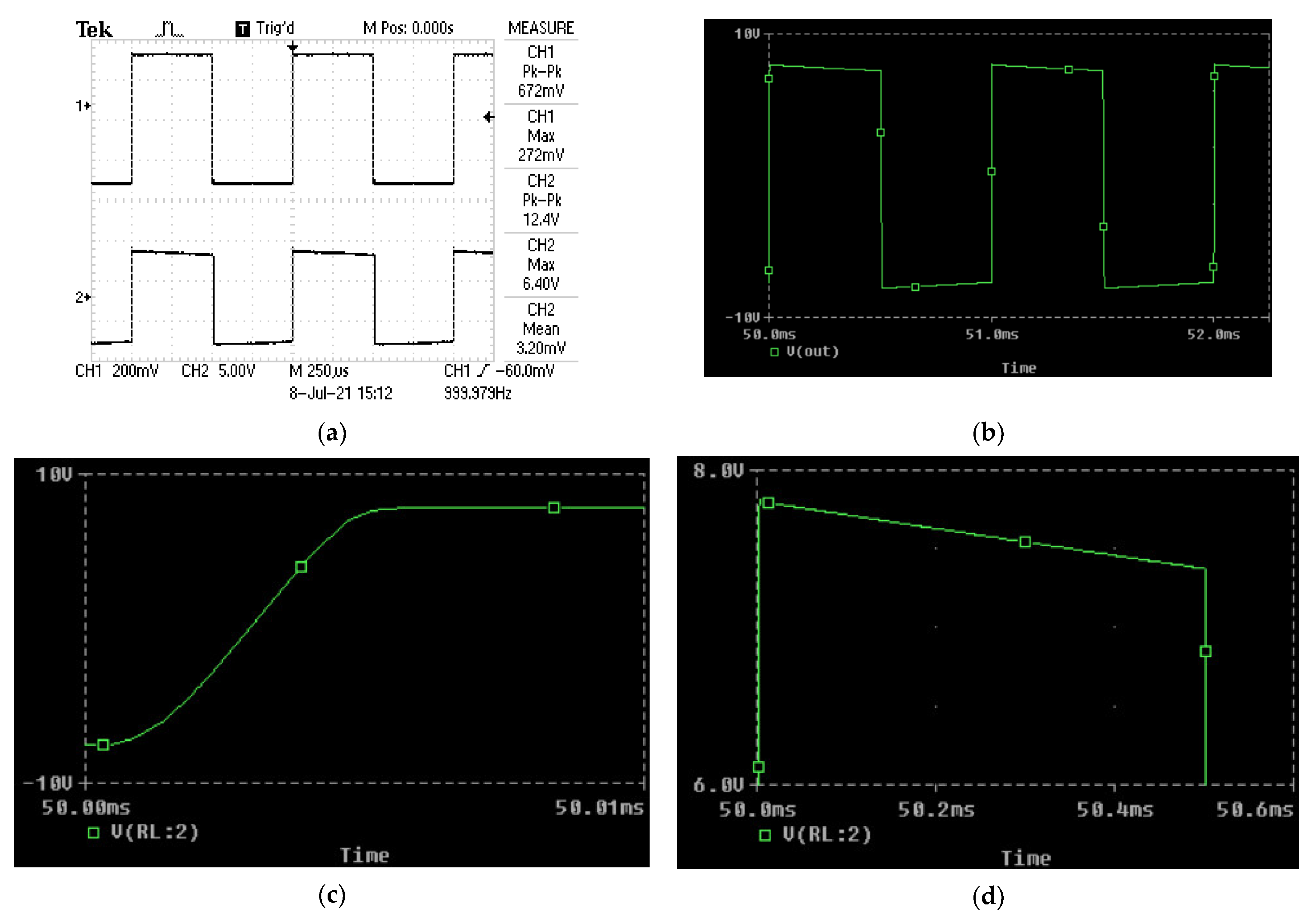
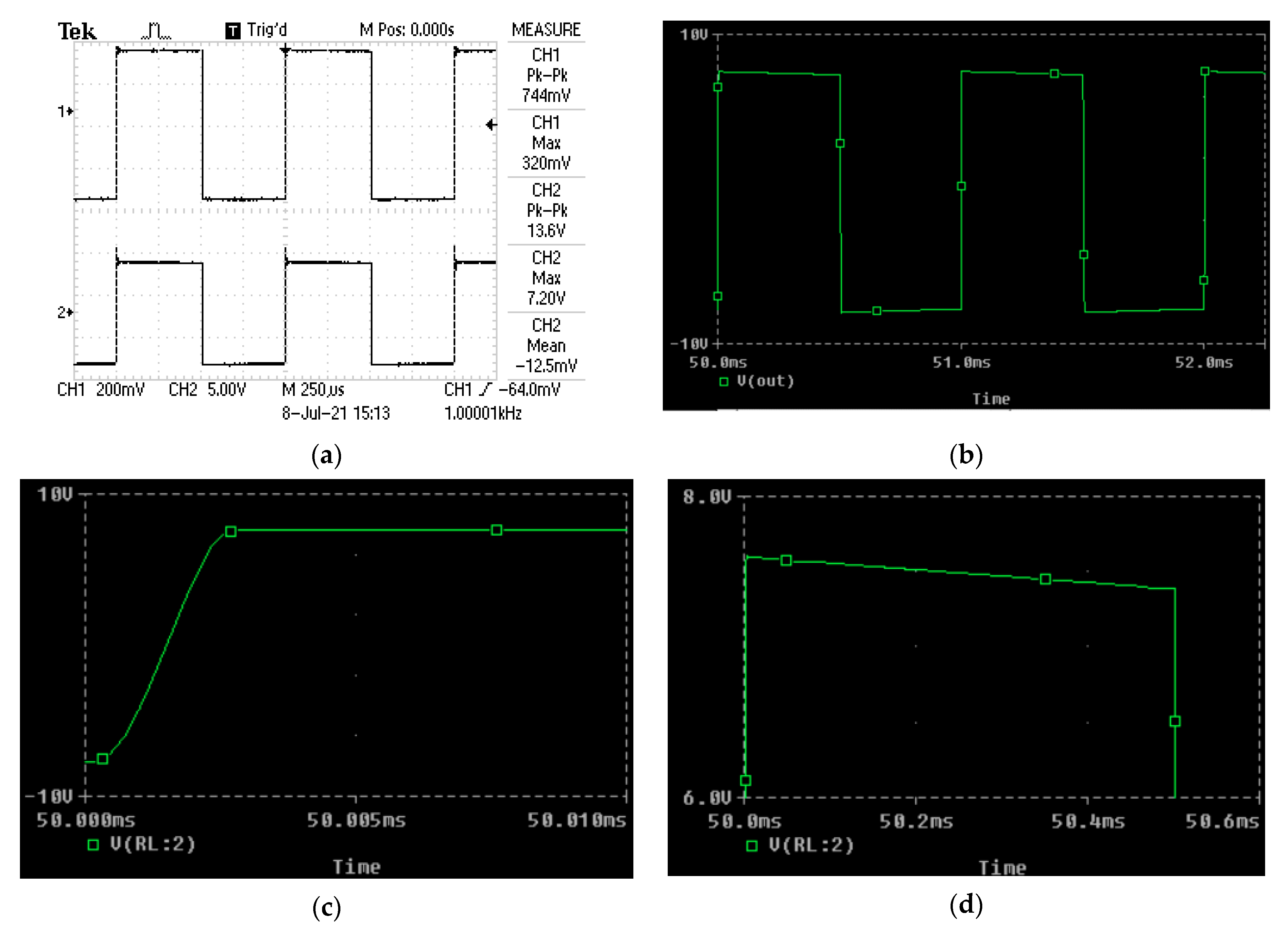
2.1. Macromodel Development
The basic technical requirements to the monolithic power amplifiers are: (1) to provide a certain electrical power to an external load, which in the general case has active and reactive components; (2) introduce minimal non-linear distortions into the wave-form of the amplified input signal; (3) to provide high energy efficiency (in this way, the greater economy is ensured, which is essential at high output power); (4) to have large input and small output resistance (this makes it easier to match the load with the output stage of the amplifier and achieves a high value of the power gain); (5) to have protection stages against short circuit or thermal overload of the output transistors. The implementation by the semiconductor manufacturers of the above requirements determines the efficiency and workability of the power amplifiers in a wide range of variations of the input voltage or power supply voltage.
Several semiconductor manufacturers, such as Maxim
®, Analog Devices
®, Philips
®, Sanyo
®, Samsung
®, SGS Thomson
®, ST Microelectronics
®, and Texas Instruments
® offer commercially available various types of monolithic power amplifiers. Some integrated circuits of the power amplifiers contain only an output stage, but often a preamplifier is included in the chip. Their basic electrical circuit is similar to those with discrete components [
11,
12,
13,
14,
15]. The passive components that cannot be integrated into the chip (such as, capacitors with high capacitance, coils, and potentiometers) are connected externally to the circuit. One of the basic monolithic integrated power amplifiers is those of the ST Microelectronics from the TDA-series [
14,
15]. The basic DC and AC parameters and their typical values for the monolithic amplifiers from TDA-series are presented in
Table 1.
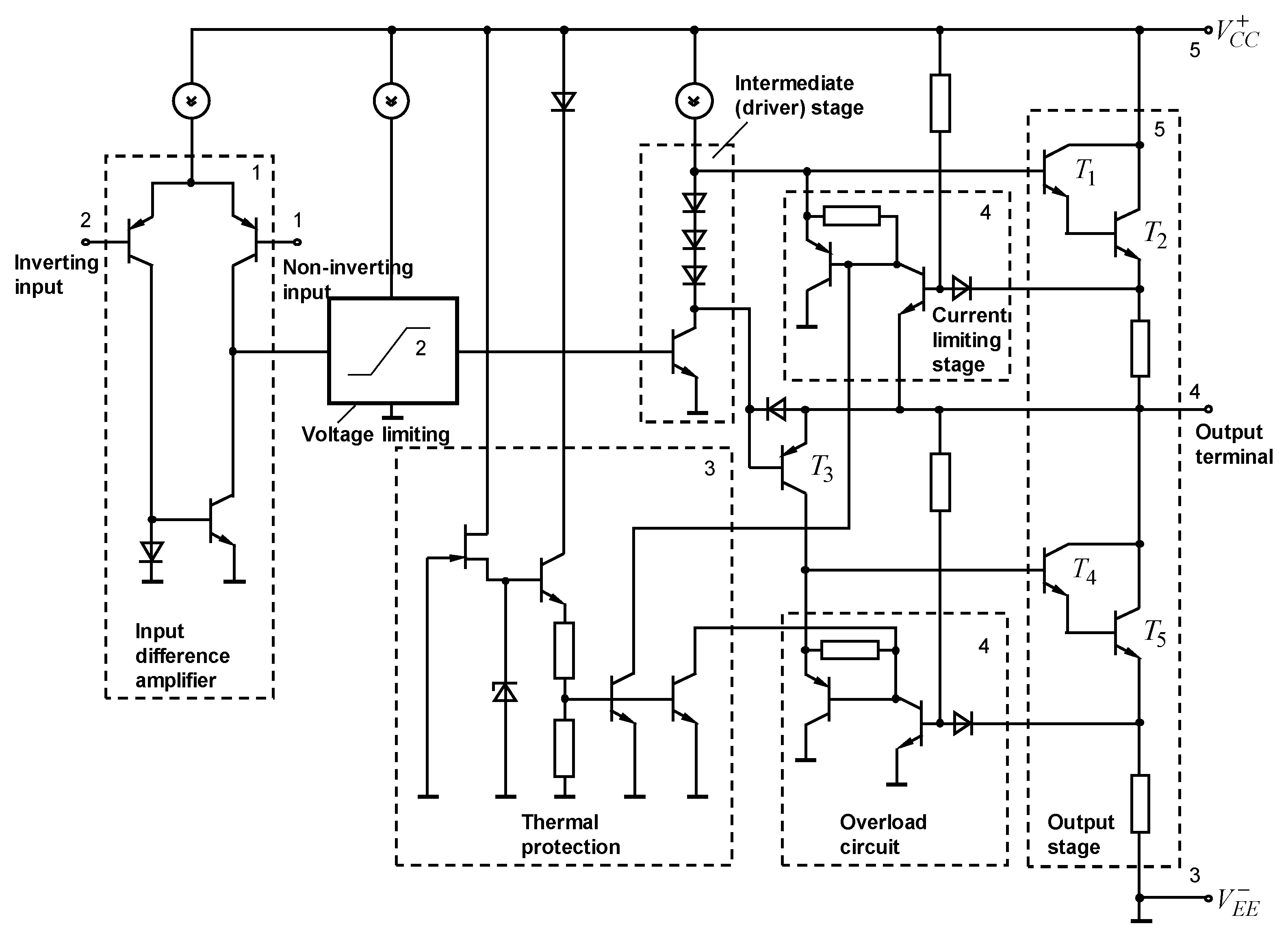
In
Figure 1 is a simplified circuit diagram of a TDA2030 power amplifier is given. As can be seen, the electrical circuit is divided into three sections (or stages): input stage, intermediate (or driver) stage and output stage. The input stage is a differential amplifier with a symmetrical input and single-ended output port. It provides the input impedance of the circuit and part of the open-loop voltage gain. The intermediate stage is an active-loaded common emitter amplifier, preceded by a voltage limiting circuit. From the output terminal of the intermediate stage, the signal is applied to the output stage. Its structure is similar to the basic output stage and includes two complementary Darlington transistors. The output stage provides the output voltage swing and output resistance. The transistors
, and
form the composite NPN-transistor according to the Darlington scheme, and the transistor
, together with the Darlington transistors
and
, form a composite PNP-transistor. In addition to the main amplifier stages, the chip also includes thermal protection and current limiting circuits.
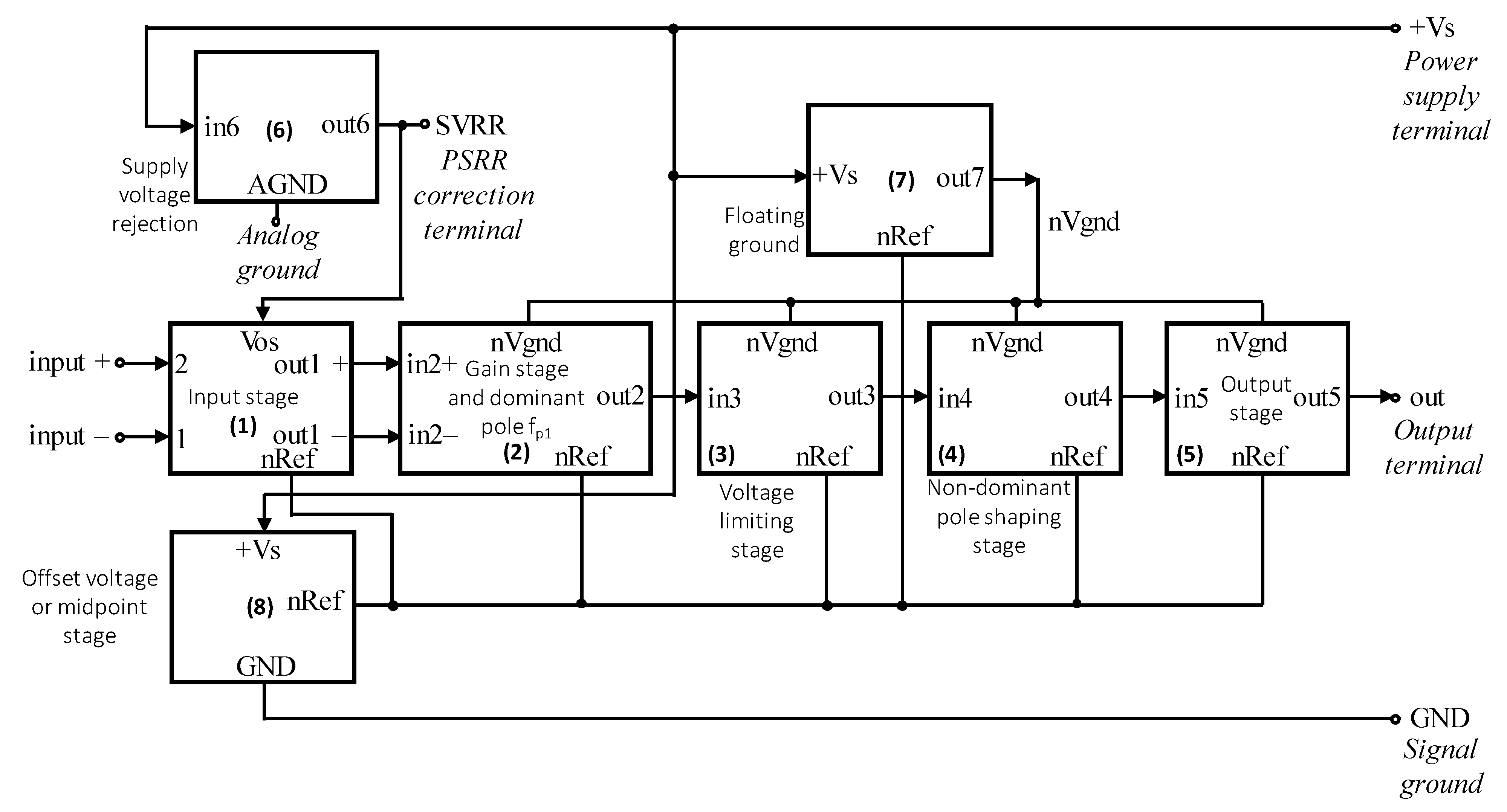
Based on the simplified circuit diagram in
Figure 1, a block diagram of the proposed model (
Figure 2) is developed. In
Figure 2, the block diagram includes basically an input stage, an intermediate (amplifying) stage, and an output stage connected in a cascade structure. Additionally, three blocks are connected to the structure, providing the midpoint of the model, the floating ground, and the supply voltage rejection ratio. According to the complexity of the amplitude-frequency characteristic of a concrete amplifier, the number of frequency-shaping stages can be increased, as well as the structure of the stage modeling the suppression of the pulsations in the supply voltage can be changed.
2.2. PSpice Implementation
To develop PSpice macro-model for monolithic power amplifiers, simplification and build-up techniques for macro-modeling of operational amplifiers was used [
1]. Based on the block diagram, shown in
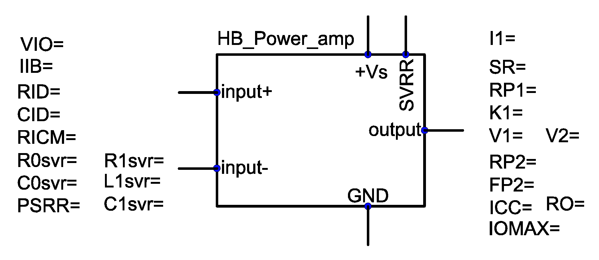
Figure 2, the macro-model was implemented as a two-level hierarchical structure. The higher-level block diagram with the modeling parameters, defined without concrete values, is presented in
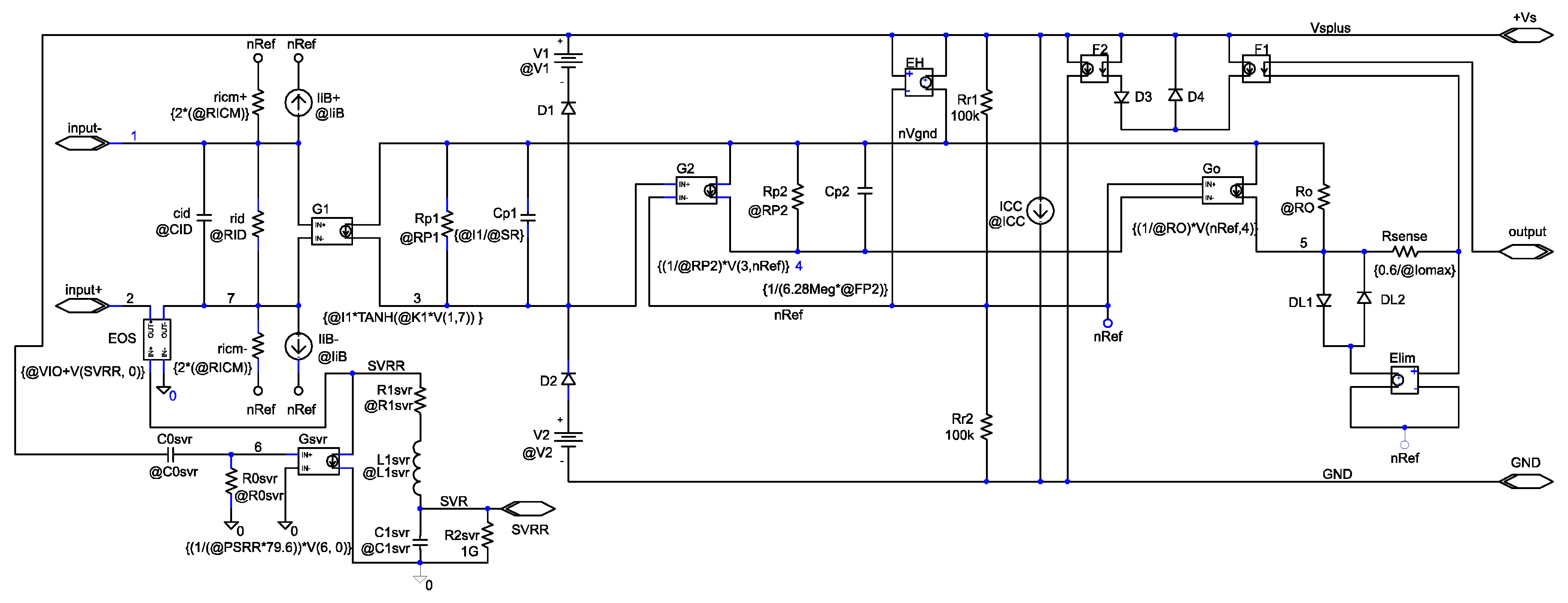
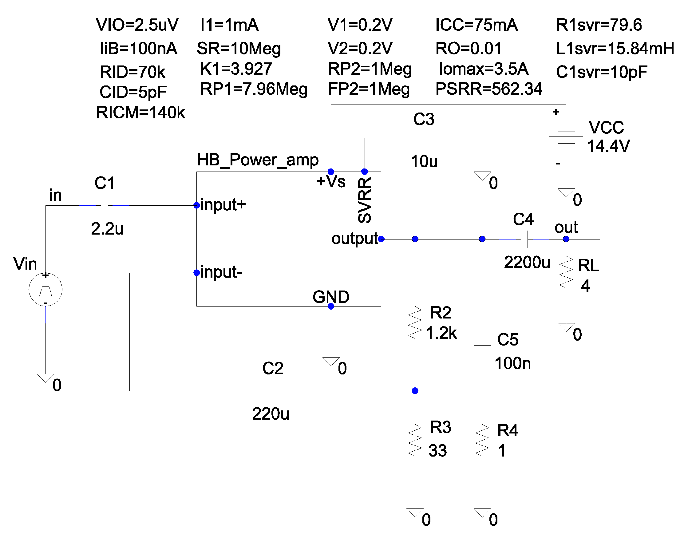
Figure 3. Depending on the choice of a certain type of amplifier in dialog mode, concrete numerical values can be set for the modeling parameters. The equivalent electrical circuit (the lower level of hierarchy) of the macro-model is given in
Figure 4. As can be seen, there is a correspondence between the names of the external terminals (or pins), and also in the description of the block diagram (
Figure 3) the name of the equivalent circuit in
Figure 4 was set, so that it can be loaded and processed during of the simulation process.
In particular, the structure of the equivalent circuit (
Figure 4) includes both standard PSpice components and analog behavioral modeling (ABM) blocks. The usage of ABM blocks, such as various controlled sources, provides the implementation of linear and non-linear mathematical functions in the PSpice program. As can be seen, the equivalent electrical circuit is represented as properly connected controlled sources, independently controlled sources, resistors, capacitors, and a small group of ideal diodes. The external interface terminals of the circuit are non-inverting input (
input+), inverting input (
input–), an output terminal (
out), supply voltage ripple rejection terminal (
SVRR), positive power supply (+
Vs), and analog ground (
GND). As can be seen, there is no ground reference in any of the signal-processing blocks. The only exception is the functional block, which simulates the attenuation of the power supply voltage ripples. All internally generated node voltages are referred to as the voltage at node nVgnd, which is the floating ground of the equivalent circuit. The node voltage nVgnd is produced by the VCVS
EH controlled by the midpoint and power supply voltage. The midpoint, called nVref in the model, was generated by two equal resistors (
Rr1 and
Rr2) connected between the supply rail and the external ground reference.
The input stage consists of
and
, modeling the input resistance and capacitance between the two input terminals (1 and 7) at a small signal.
and
are the input resistances, reflecting the behavior at a common-mode input signal. The input resistance
is defined as the resistance measured directly between the inverting and non-inverting input of the amplifier:
at
.
In the case of an amplifier circuit with asymmetric input, a circuit of a non-inverting amplifier with a grounded inverting input and an active non-inverting input are possible, and vice versa—a circuit of an inverting amplifier with a grounded non-inverting input.
The input resistance in these cases is represented by
The input common-mode resistance is represented, according to
For the majority of the amplifiers .
The input bias current was modeled by two ideal current sources (
and
), connected between the two input terminals (1 and 7) and midpoint nVref. The input offset voltage and offset drift as a result of the power supply ripples is represented with a voltage-controlled voltage source (VCVS)
, connected between nodes 2 and 7. The offset voltage modelling power supply ripples (PSRR—power-supply rejection ratio), which are accurately referred to the VCVS
, come from two separate frequency shaping stages in the model. The first additionally defined stage consisted of a capacitor
and a grounded resistor
. The
is connected between the power supply voltage (node Vsplus) and the input of the second shaping stage. The voltage drop over the
presents the voltage at a node 6 that depends on the ripples of the supply voltage (
). The transfer function of the stage is expressed by
The second stage consisted of a voltage-controlled current source (VCCS)
controlled by the power supply voltage, and the
RLC-stage. The current source was chosen to be linear one-port generator, following the equation
The current
will flow through the elements
,
, and
(where
is an external grounded capacitor, connected to node
SVR), towards the internal ground. In such a way, the voltage
V(
SVR,0) will depend on the amplitude and the frequency of the ripples of the supply line, and the transfer function of the stage can be expressed by
where
is DC proportionality constant,
is the time-constant of the polynomic in the numerator,
is the damping factor, and
is the time-constant of the polynomic in the denominator.
From the comparison of the left and right sides of the above equation, the following formulas were obtained for the main parameters:
,
—time constant determining the minimum in the frequency response,
and
, where
is equivalent series inductance,
is equivalent series capacitance, and
is equivalent parallel resistance. The proposed stage from
Figure 4 provides a serial resonance, determined by the inductance
, and the capacitance
, with a minimum value of the resonance resistance. The voltage generated at node SVRR is used for the equation of VCVS
as follows
The component
in Equation (6) determines the input offset voltage constant (
), the coefficient
presents the change in
as a result of changing the supply voltage. Then,
will be determined by the following expression
where
is the differential voltage gain of the amplifier and
is the voltage gain of the ripples in the power supply line.
The intermediate stage of the model consisted of controlled sources and ideal passive components. It simulated the open-loop voltage gain, the frequency resonance, and the output voltage limiting. The value of the open-loop voltage gain of the model is represented by the VCCS
, and the resistor
. Therefore, the voltage at a node 3 can be determined by
where
is the multiplication factor of the stage.
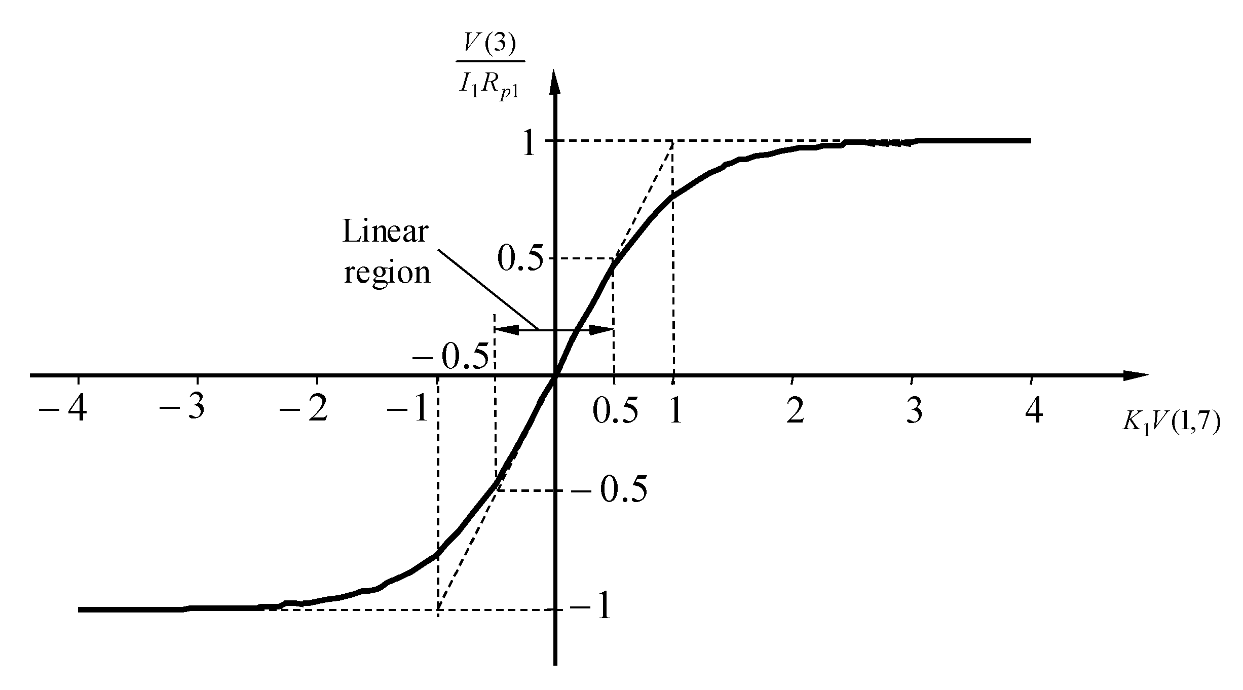
The transfer function (9) is represented in graphical form in
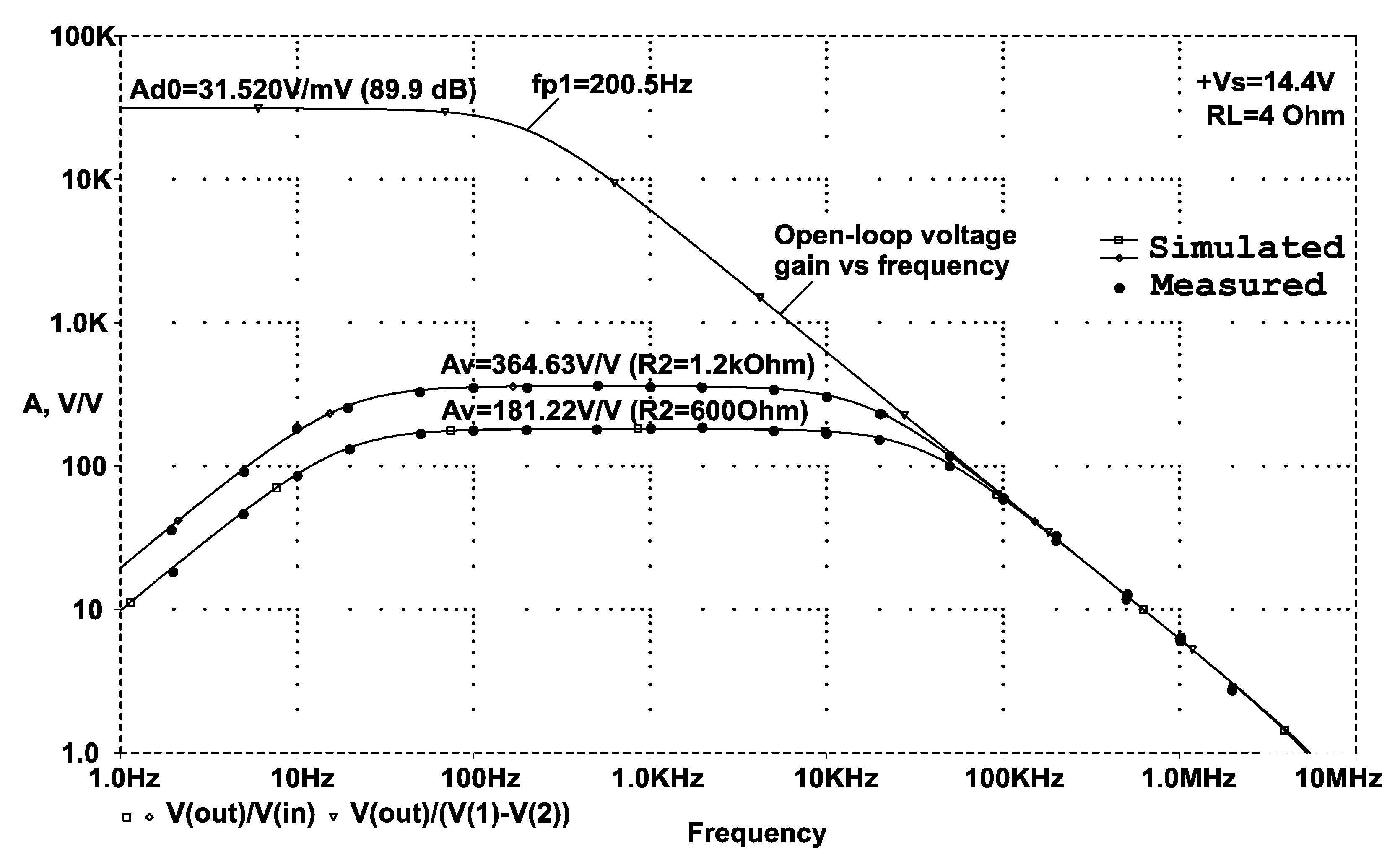
Figure 5. Approximately linear region of this function is
.
The simplification of expression (9) can be performed if the function is decomposed in the Taylor order, i.e.,
at
.
If
, elements can be taken only up to the third order term in the Taylor series, wherein the formula (9) yields
If
, the
. The maximum output current
charged the capacitor
, which created a change of the output voltage per unit time of the amplifier. This rate of change of the voltage per unit time defined the maximum
dV/
dt (voltage change rate) or slew rate (or SR) of the amplifier:
For the model’s small-signal open-loop DC voltage gain, is obtained
To obtain minimal nonlinear distortions in the waveform of the output voltage (), it is necessary that the input voltage is lower than . Since the mathematical function is symmetric with respect to the origin of the coordinate system, and with respect to the characteristics of the differential pair of transistors in the input stage (transistors have to be as close as possible to technological parameters, which is achieved by applying a single technological process of obtaining the electrical circuit), for the developed macro-model it is possible to obtain smaller values of the nonlinear distortions.
The voltage-limiting network consisted of two ideal diodes (
and
) and two voltage sources (
and
), connected in series. This network limited the voltage at node 3 and the other internal voltages of the macro-model up to values below the power supply voltage during an input-overdrive condition:
where
is the thermal voltage and
is the saturation current for the two diodes.
The first (dominant) and the second pole frequency are represented in the model by two frequency shaping stages. The dominant pole was modeled by the VCCS
, the resistor
and the capacitor
. The second (non-dominant) pole was modeled by the VCCS
, the resistor
and the capacitor
. The DC voltage gain of the second frequency-shaping block was equal to unity, because the
of the VCCS
is equal to the reciprocal of the resistance
, connected from each node of the VCCS to the floating node of the circuit. In a wide frequency range, the open-loop amplitude-frequency response of the model can be represented by
where
is the first pole frequency and
is the secondary pole frequency.
The output stage of the model consisted of controlled sources and passive components provided the output signal. It simulated the output resistance and the DC and dynamic of the current consumed by the external power supply device. The VCCS in the output block drives the resistor , connected between the node 5 and the floating ground. The acted as an active current generator and provided the desired voltage drop over its parallel resistor. The DC voltage gain of the output block was equal to unity, because the of the VCCS was equal to the reciprocal of the resistance .
The limitation of the output current was presented in the macro-model through the controlled voltage source
, the resistor
, and the pair of diodes
and
[
16]. When the voltage drop across the resistor
becomes approximately equal to 0.6 V, one of the two diodes (
or
) turns on and the current is limited to
.
When there is no load at the output, the model draws only a quiescent current from the power-supply rail by the independent current source
in the model, thus behaves similarly to an ideal class-B output stage with a gain equal to unity. When an AC voltage is applied to the input port, as a result of the amplification, the output voltage will have greater amplitude, which is obtained by increasing the power consumption. In the proposed model, the dynamic behavior of the supply current is produced through a pair of current-controlled current sources (CCCSs) (
and
) with unity gain and a pair of ideal diodes (
and
), similar to the op amp models, presented in [
2,
3,
6]. The
is controlled by the magnitude of the output current through the load, which in turn generates a current, driving the two diodes. Depending on the magnitude and the direction of the current through the
F2, an AC current flows from the power supply to the ground, which average value
is proportional to the real consumed current. Another technique for modeling the supply current variations is by using relatively complex high-order (
n > 2) nonlinear current source
F2 [
4].


