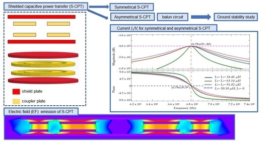
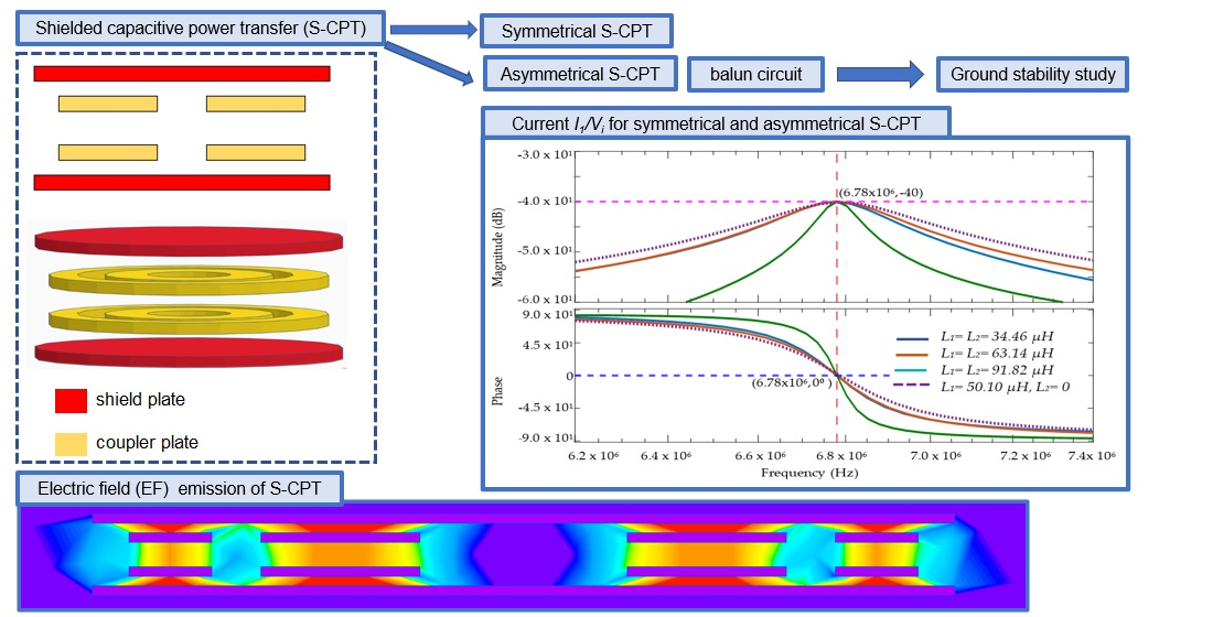
2. S-CPT System
A generalised circuit of S-CPT can be formed into symmetrical and asymmetrical topologies in which the symmetrical topology has advantages in terms of the stability of the load changing, whereas the asymmetrical topology has the advantage of being lightweight at the receiver side [
20]. Symmetrical and asymmetrical S-CPTs systems must be designed in resonance and matching conditions as the major design requirements. In the resonance condition, the S-CPT system has a total impedance of the resistive part with zero reactance part, with a total admittance equal to 0.01 in the matching condition for transferring maximum power [
20].
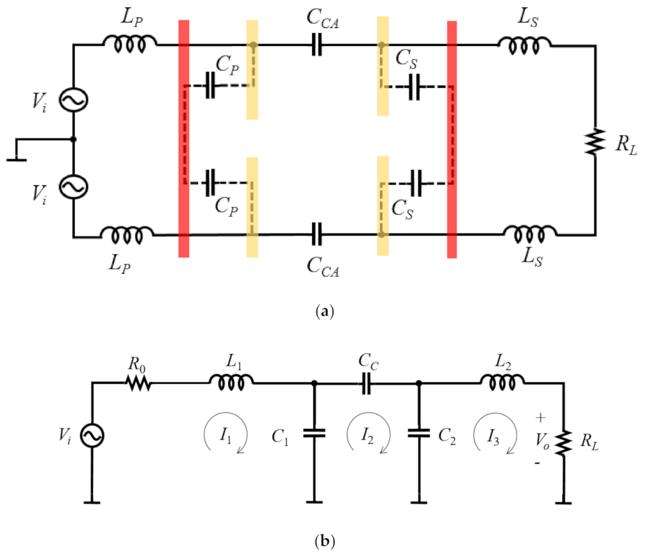
Figure 2a shows the S-CPT system with an inductor at both the primary and secondary sides. Eliminating the inductor on the secondary side transforms the symmetrical circuit into an asymmetrical topology. The inductor’s internal series resistance affects the total current in S-CPT in terms of loss and efficiency [
20]. Eliminating the secondary circuit resulted in a lightweight and compact S-CPT design. Therefore, for applications such as drones and robots that must be lightweight, the symmetrical topology has a potential solution for wireless power transfer. Accordingly, this study focused on the asymmetrical configuration and investigated the ground voltage stability and EF emission.
Figure 2a shows the component arrangement in the S-CPT system, in which the capacitance represents the six-coupler plate structure with a voltage input
Vi and load resistance
RL. The capacitance of the S-CPT structure is modelled by the primary coupler to the secondary coupler and the parasitic capacitance between the coupler and shielding plate only. Other parasitic characteristics were excluded—such as cross-coupling capacitance, edge side-to-side capacitance, and shield plate to ground capacitance—from the analysis. Therefore,
Figure 2a presents the capacitance model, with
Cc as the capacitance between the coupler plate and at the primary and secondary sides. The parasitic capacitance at the primary
CP is the capacitance between the coupler plate and shielding plate. The parasitic capacitance
CS is the capacitance between the coupler and the shielding plate at the secondary part. The inductor
LP is placed on the primary side, and the load
RL is located in the secondary part. On the secondary side, the inductor
LS is connected to the load. The S-CPT circuit diagram can be simplified into an equivalent circuit [
20], as shown in
Figure 2b, by mirroring the
x-axis structure shown in
Figure 2a.
Figure 2b shows the equivalent circuit of S-CPT to represent the symmetrical circuit, as shown in
Figure 2a, where
R0 is the internal characteristic of the power source.
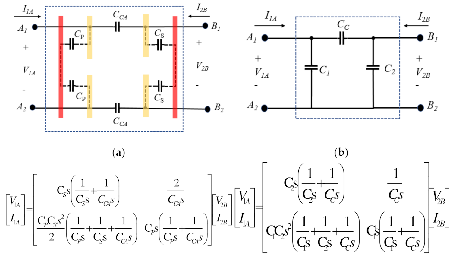
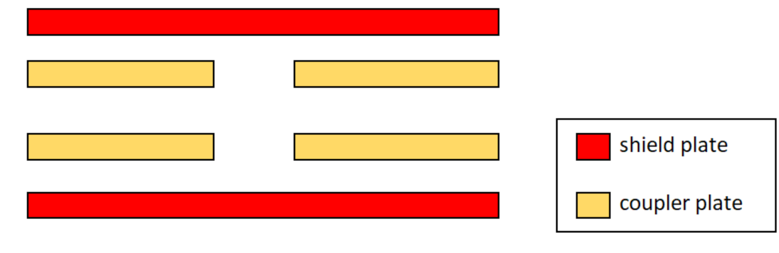
Figure 3a shows the coupler structure of S-CPT with four coupler and two shield plates, and
Figure 3b shows the equivalent circuit of the coupler. In
Figure 3b, the capacitance
C1 is denoted by the total series capacitance
CP on the primary side.
The secondary capacitance,
C2, equals the total series of inductor C
S. Obtaining the capacitance parameters shown in
Figure 3b involves using the two-port network method, assuming that both circuits in
Figure 3a,b have the same value as the ABCD transmission parameter matrix as in Equation (1) and
s =
j *
ω, in which
ω is the angular frequency. Solving both circuits in
Figure 3 using a MATLAB simulation with the same parameters of the ABCD matrix implies Equation (2) provides the coupling capacitance
Cc, whilst Equations (3) and (4) provide the primary and secondary capacitances, respectively.
When the inductor at the primary
L1 is inserted at the circuit, as shown in
Figure 2b, the inductor in
Figure 2a will become half of
L1 because the total inductors for both circuits are the same. In the simplification expression,
LP = 0.5 ×
L1, and
LS = 0.5 ×
L2. On the secondary side, the secondary capacitance
C2 and secondary inductor
L2 are denoted by the total series capacitance
C2 and double value of the secondary inductor
LS. Therefore, the equivalent circuit shown in
Figure 2b is formed from
Figure 2a based on the relationship between the parameters. In
Figure 2b, the Kirchhoff voltage law (KVL) represents
I1,
I2, and
I3. Using the same analysis as described in [
20], the KVL equations of
I1,
I2, and
I3 can be obtained as in Equation (5). Solving the expressions of
I1,
I2, and
I3 involves using linear methods with a variable method, and the current to voltage equation,
I1/
Vi, can be obtained as in Equation (6).
where
.
The ratio of the secondary capacitor C2 to the primary capacitor C1, r = C2/C1, and the relationship between the coupling capacitance and the shield coupler is a = 1 + C/Cc + 1/r.
The value of the operating frequency f and angular frequency ω = 2πf. The value C is equal to the primary capacitance, C = C1.
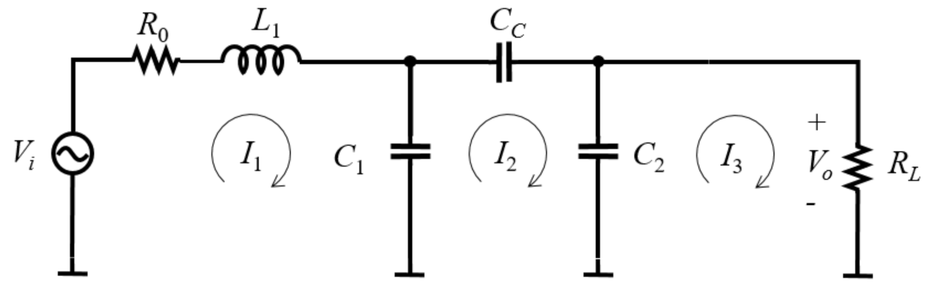
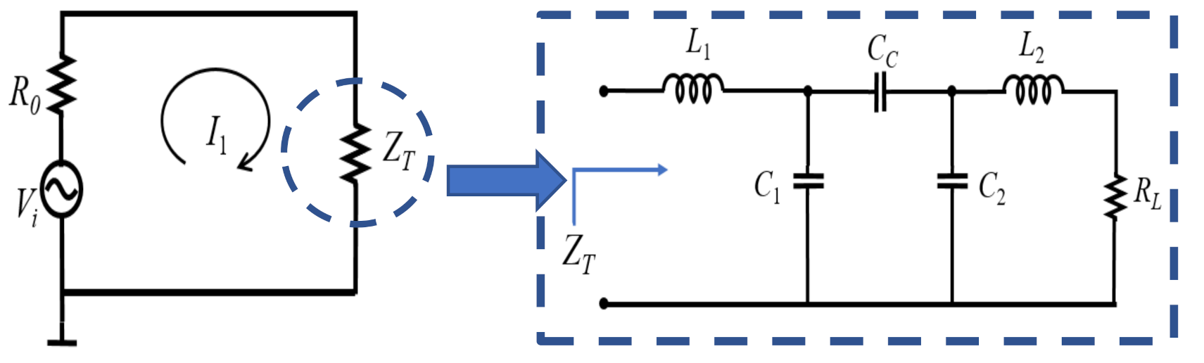
Two approximations have been used to analyse and simplify the S-CPT circuit. First, total impedance can be calculated if a resonance condition occurs in the circuit with the assumption that all components in the S-CPT system are modelled by the single impedance
ZT. Second, the match impedance condition in which the impedance at the input is equal to the output impedance by considering that the input power supply device has a match impedance load to S-CPT. Therefore, the equivalent circuit in
Figure 2b can be simplified into a series circuit, as shown in
Figure 4, in which it is arranged with total impedance
ZT. The circuit consists of the total impedance
ZT as the output impedance, voltage source
Vi with an operating frequency
f, and internal series resistance
R0 as the input load.
Figure 4 shows the simplified circuit model for the analysis process, assuming that the circuit is in the resonance and match impedance conditions. In the resonance condition, the total impedance
ZT is given by the resistive part with zero reactance. In the match impedance circuit, the impedance
ZT is equal to the input impedance
R0 to transfer the maximum power. Therefore, the
I1/
Vi shown in Equation (6) is solved in the resonance condition to deduce the inductor value by taking the total reactance in the circuit to be equal to zero, in which the total circuit impedance is contributed by the resistive part with no imaginary part. In the match impedance condition, the magnitude of current to voltage, |
I1/
Vi|, is equal to 1/100 or 0.01 [
19] by taking both the input internal resistance and output load impedance equal to 50 Ω, in which the total impedance is equal to 100 Ω. Therefore, the S-CPT system in this analysis considers a 50 Ω impedance match between the supply load and S-CPT load.
In the symmetrical circuit, the primary inductor
L1 is equal to the secondary inductor
L2, whereas the shield plate capacitance at both the primary and secondary parts are the same,
C =
C1, with the ratio of the primary capacitance to the secondary capacitance
r = 1. Therefore, the deduced inductor value that uses Equation (2) with the resonance condition is obtained in Equation (7). A MATLAB simulation was used to perform the calculation process.
Equation (7) shows the relationship between the inductor and other parameters, which shows that the symmetrical circuit produces three possible values of inductors in which it can be formed into three topologies of symmetrical S-CPT. In reference to Equation (7), one of the S-CPT systems has no relationship between the
RL load and the inductor value, whilst the other two systems have a relationship between the inductor and the
RL load. Based on the symmetrical S-CPT analysis, the S-CPT topologies are formed into asymmetrical topologies, as shown in
Figure 5.
Figure 5 shows asymmetrical S-CPT in which the primary inductor
L1 is arranged with the shield plate capacitance
C1 and
C2 and the coupling capacitance
CC with no inductance at the secondary side. Therefore, the primary inductor
L1 can be expressed in Equation (6) by having the secondary inductor
L2 equal to zero and the obtained equation calculated as in Equation (8).
Equation (8) shows the relationship between the primary inductor
L1 and other parameters in the S-CPT system. Further analysis was performed to calculate the inductor value in both symmetrical and asymmetrical topologies using the analysis test parameters listed in
Table 1. Moreover, these topologies were tested in a simulation to study the performance of the resonance and matching impedance conditions.
Table 1 lists the analysis test parameters for both the symmetrical and asymmetrical circuits. An operating frequency of 6.78 MHz is selected with a 50 Ω load. The S-CPT system uses an operating frequency of 6.78 MHz, which is the lowest value used for the industrial, scientific, and medical bands for MHz wireless power transfer. The International Telecommunication Union Radio recommends an operating frequency of 6.78 MHz because it has little or no negative effect on other licensed bands [
19]. The primary capacitance C
1 and the secondary capacitance C
2 with the ratio
r = 1 is selected in the analysis study. The relationship between the coupling capacitance and the shield coupler is given by
a = 3.2.
Based on the analysis of the calculation process in the MATLAB simulation, the inductor value was obtained. In symmetrical S-CPT, Equation (3) was used to calculate the inductor’s value both at the primary and secondary sides as 34.46 µH, 63.14 µH, and 91.82 µH. Symmetrical S-CPT has three different values of inductor for the three topologies of symmetrical S-CPT, as discussed in the analysis section. In the asymmetrical S-CPT analysis, Equation (8) was used to calculate an inductor value at the primary side with zero inductance value at the secondary side.
Table 2 presents the results of the analyses.
Table 2 shows the calculated results obtained from the MATLAB simulation. The analysis parts with calculated inductor values show that S-CPT can be formed into symmetrical and asymmetrical topologies. Symmetrical S-CPT has three topologies, considering the three different inductors, whereas asymmetrical S-CPT has an inductor value at the primary but no inductor at the secondary.
Based on the findings of the analysis,
I1/
Vi, as in Equation (6), was used to further analyse the symmetrical and asymmetrical S-CPT with the calculated values and parameters in
Table 1. The magnitude |
I1/
Vi| for S-CPT was simulated in MATLAB software using the value of inductors, as shown in
Table 2. The simulation of |
I1/
Vi| was performed to investigate the resonance and matching impedance conditions of the S-CPT system in both symmetrical and asymmetrical topologies.
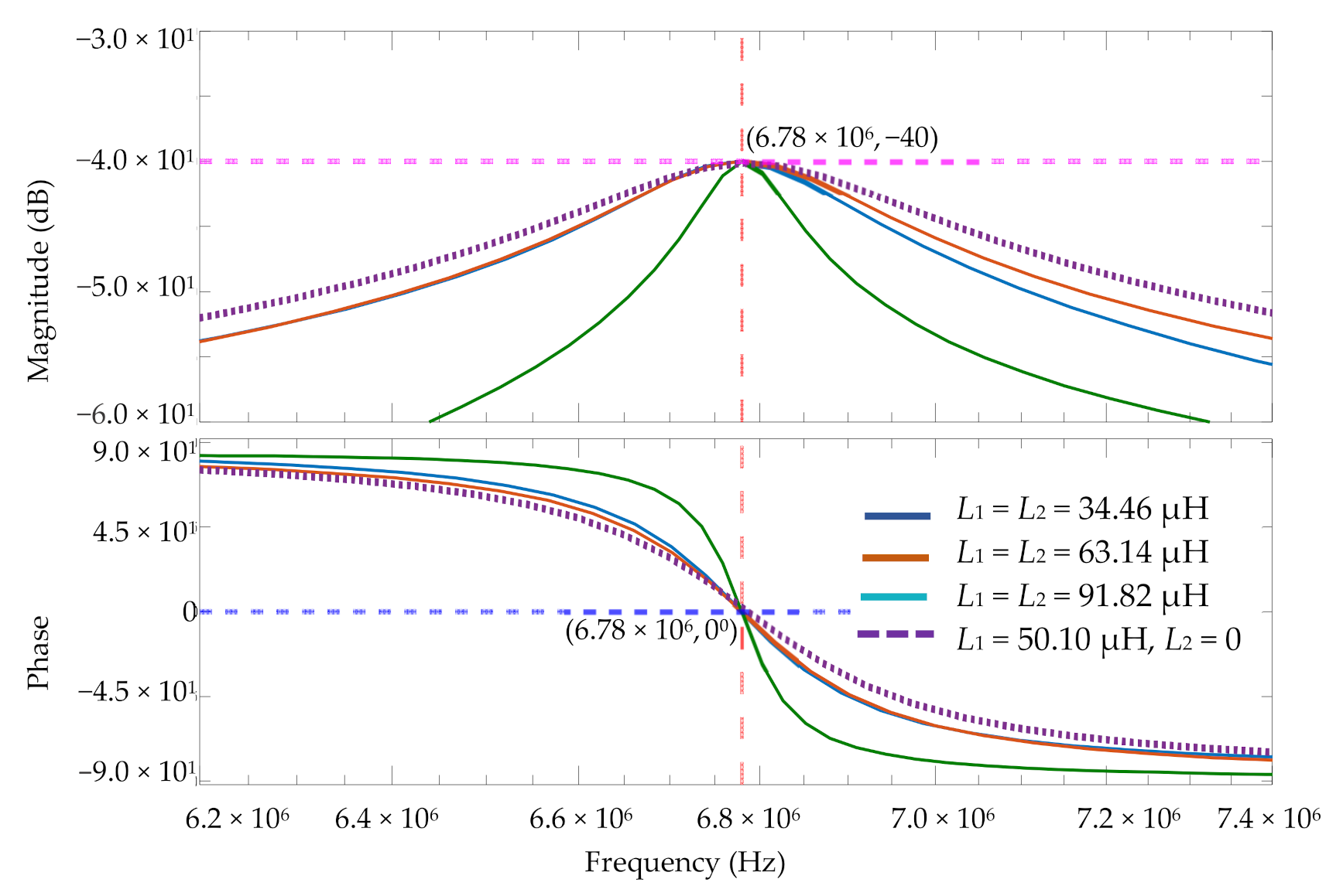
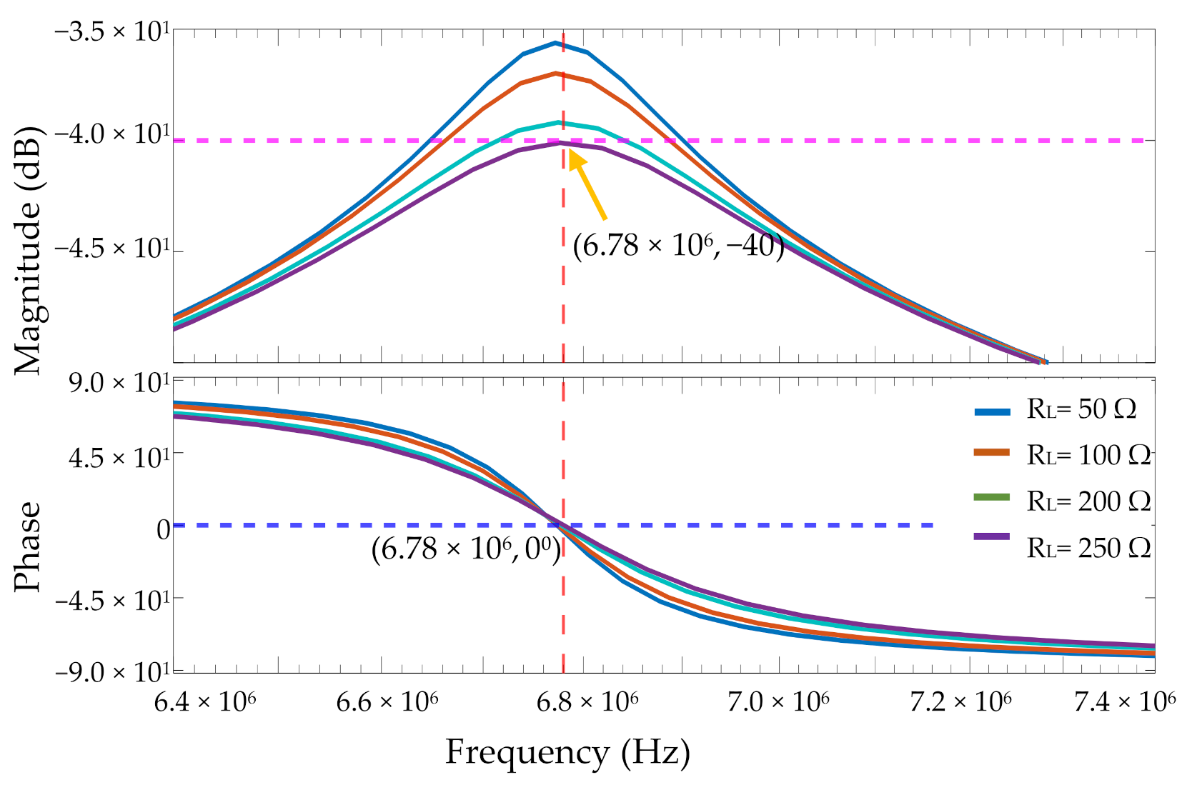
Figure 6 plots the results obtained based on the simulation.
Figure 6 shows the magnitude and phase of
µH I1/
Vi for symmetrical S-CPT (
L1 =
L2 = 34.46 µH, 63.14 µH = 91.82 µH) and asymmetrical S-CPT (
L1 = 50.10 µH,
L2 = 0). A straight line plotted in the graph at the
x-axis of 6.78 MHz shows the operating frequency. In the phase part, all the topologies have the same value of 0° at 6.78 MHz. In the resonance condition, the current to magnitude |
I1/
Vi| is 0° in phase owing to the total impedance of S-CPT, and
ZT has a resistive part and zero reactance. Therefore, the line plotted along the
y-axis at the 0° phase serves as a reference to the obtained result. The result shows that both symmetrical and asymmetrical topologies are under the resonance condition by the plotting graph passing through the 0° phase at 6.78 MHz.
The S-CPT topology is under the match impedance condition at the magnitude of |
I1/
Vi| = 0.01 [
19,
20] or −40 dB, as discussed in the analysis section by referring to
Figure 4, in which S-CPT has a match impedance between the input and output impedances to maximise the power transfer.
Figure 6 shows the magnitude of both the symmetrical and asymmetrical S-CPT topologies approaching −40 dB at 6.78 MHz. In the match impedance condition, the total impedance
ZT equals the internal series resistance of the power supply
R0. Symmetrical S-CPT B (
L1 =
L2 = 63.14 µH), as shown in
Table 2, approaches −40 dB at 6.78 MHz or in the match impedance when the load equals 30 kΩ because the inductor has no relationship with the load resistance
RL, as reflected in Equation (2). Therefore, S-CPT B has an effective load of 30 kΩ to obtain the match impedance condition. S-CPT A and S-CPT C have an effective load of 50 Ω, and asymmetrical S-CPT has an effective load of 250 Ω. The effect of the load on asymmetrical S-CPT was studied and the results of the magnitude and phase
|I1/Vi| are presented in
Figure 7.
The values of the parameters in asymmetrical S-CPT were calculated under resonance and match impedance conditions. The circuit must comply with both resonance and match impedance conditions to ensure the best performance of the system. Therefore, Equations (6) and (8) were used, and the graph shown in
Figure 7 was plotted to calculate the inductor
L1. The value of the load resistance,
RL, was adjusted from 50 Ω to 250 Ω to obtain the best fit at the 0° phase and −40 dB for the resonance condition and the match impedance condition, respectively. As shown in
Figure 7, through a MATLAB simulation, the obtained load was determined to be 250 Ω, and symmetrical S-CPT attained the resonance condition and match impedance at 6.78 MHz. Notably, when the load resistance is 250 Ω, the magnitude value of |
I1/
Vi| approaches 0.01, or −40 dB, at 6.78 MHz with 0°. Therefore, S-CPT works in maximum power transfer with a load resistance of 250 Ω. In different applications with different loads, an additional matching impedance circuit is required to match the output of S-CPT to the application.
In the simulation, the symmetrical and asymmetrical topologies demonstrated a good agreement between the analysis and simulation results. It found that S-CPT can be formed into symmetrical and asymmetrical topologies. Therefore, the work proceeds with the asymmetrical S-CPT topology to investigate the hardware performance using the experimental setup.
In designing the asymmetrical S-CPT system, the coupler capacitance (
Cc) and capacitance of the shield coupler (
C1 and
C2) were determined based on the coupler size;
Table 3 lists the design values. The resistance load
RL at 250 Ω was selected as the calculated load obtained in the analysis.
Table 3 lists the design and measurement values of S-CPT, which are the calculated and hardware measurement values. The hardware value was determined by measuring the fabricated coupler. The parameters show a slight difference between the design value and hardware value owing to the fabrication process of the coupler and inductor.
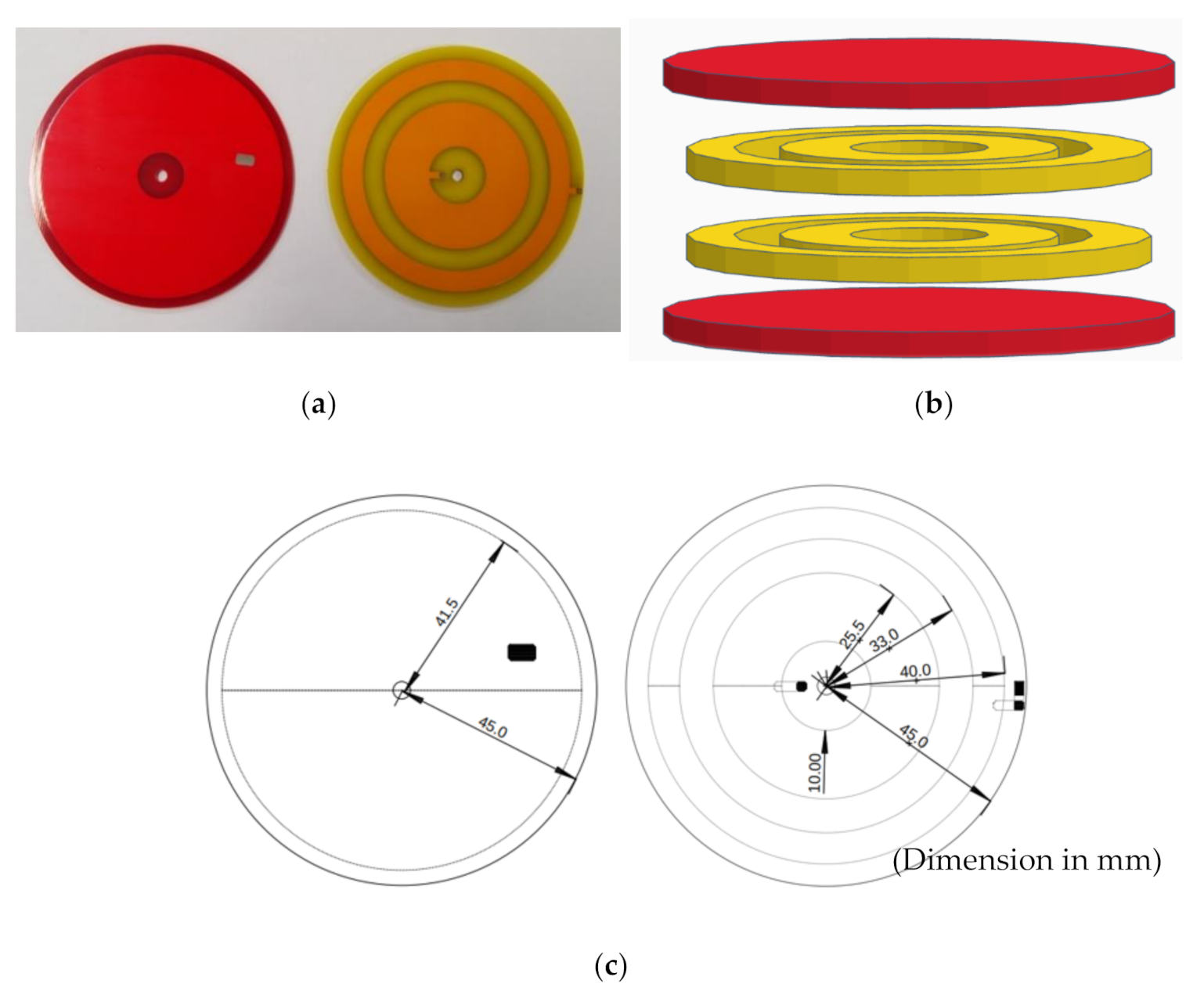
2.1. Coupler Structure
A four-coupler structure with a shielding plate was designed and fabricated, as shown in
Figure 8.
Figure 8a shows the S-CPT system fabricated on a printed circuit board comprising FR4 material with a thickness of 1.6 mm.
Figure 8b shows the shield plate and coupler plate arranged in parallel, using air as the dielectric.
Figure 8c shows the dimensions of the coupler design. The gap between the couplers was adjusted to meet the design value, as shown earlier in
Table 1; the measured hardware value indicates that the fabricated coupler has a tolerance of +3% from the design value.
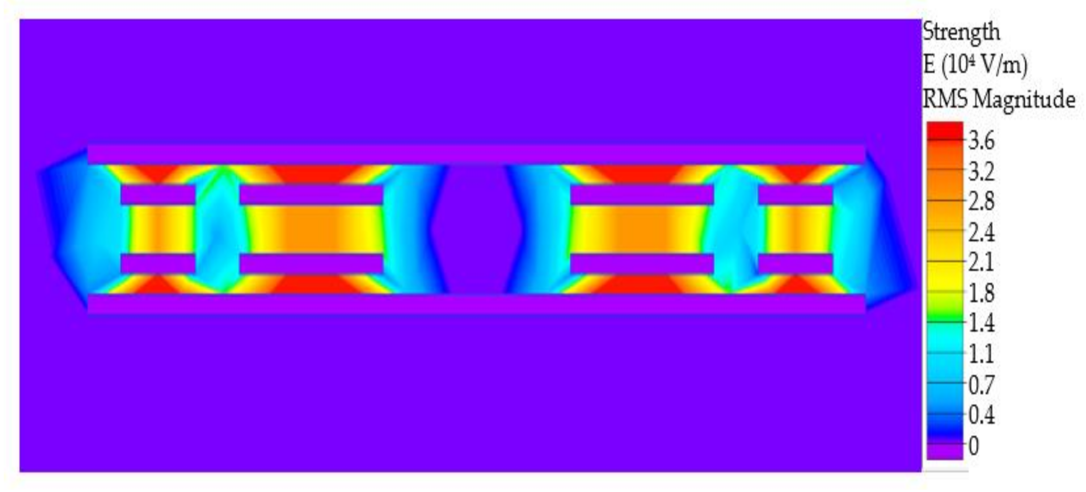
Figure 9 illustrates the EF emission in the S-CPT coupler with the actual dimensions of the fabricated coupler, as shown earlier in
Figure 8c, in which the gap between the shield plate and coupler is 1 mm, whilst the gap between the coupler and coupler is 2.5 mm. Quick Field software was used to simulate the EF emission with the actual fabricated dimensions and with the material properties between the plate and the air. The loading source and model class in the simulation was set to AC conduction and plane parallel, respectively. Furthermore, the frequency of 6.78 MHz was set with the measurement in mm value in the Cartesian coordinate system and the voltage at the coupler plate to 50 V for analysis purposes.
Figure 9 shows the EF emissions.
In
Figure 9, the EF emission behind the shield plate is between 0 and 1 kV/m. EF emission occurs inside the coupler and at both the edges of the coupler. Based on the analysis result, the coupling and shield plates emit an EF with a maximum value of 35.4 kV/m, whereas the coupler-to-coupler has a maximum EF value of 28.3 kV/m. Moreover, an air breakdown voltage occurs when the EF reaches a limit value of 3000 kV/m or 30 kV/cm [
19]. Therefore, the coupler design is under the breakdown voltage limit with a maximum EF emission of 35.4 kV/m. The simulated results also show that the shield plate in the S-CPT system minimises the EF reduction and acts as a safety feature in the system.
The International Commission on Non-Ionizing Radiation Protection (ICNIRP) guidelines set the exposure EF emission limit for humans to meet the safety requirements in designing S-CPT [
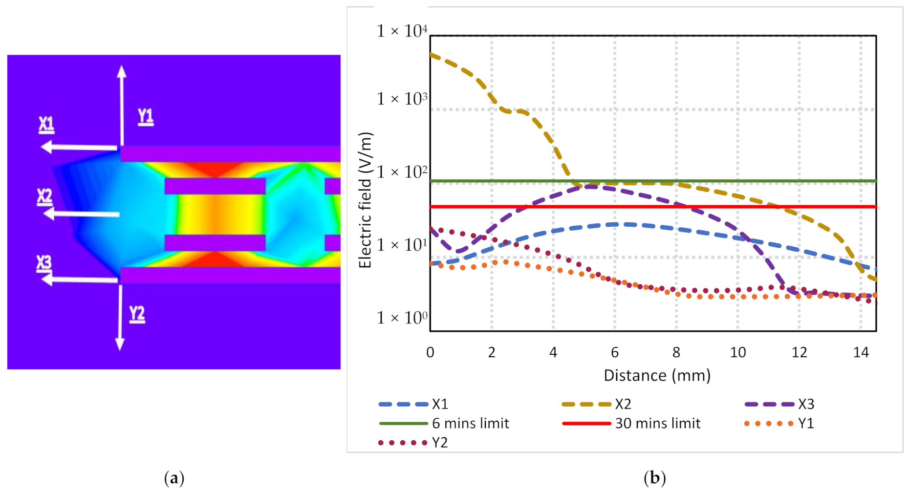
22]. According to the ICNIRP guidelines, the EF emission with a 13.56 MHz frequency to the general public is 108.18 V/m and 48.48 V/m for 30 min and 6 min, respectively. Therefore, the EF emission was measured at the coupler edge to study the safety distance from the coupler.
Figure 10 presents the data.
Figure 10 shows the electric emission at the edge of the S-CPT plates in which the measurement was performed on the
x- and
y-axes. The electric measurement was considered from 0 to 14.5 mm from the edge to study the electric field emission.
Figure 10a shows the electric field emission measurement from the edge in the
y-axis at the top shield point Y1 and bottom shield point Y2. Points X1, X2, and X3 show the measurement in the
x-axis at the top shield and the centre point between the shield plate and bottom shield plate, respectively.
Figure 10b shows the EF emission results at the edge, with the public exposure limit plotted at 108.18 V/m and 48.48 V/m in the graph. Notice in
Figure 10b that the safe distance from EF emission is 12 mm from the coupler both at the
x- and
y-axes because the EF emission values from points X1, X2, X3, Y1, and Y2 are below the EF exposure limit. Y1 and Y2 indicate that the shield plate in S-CPT acts as a safety feature, with the EF emission values from 0 mm to 14.5 mm under both 108.18 V/m and 48.48 V/m. However, on the
x-axis, the safe condition from EF exposure was 12 mm from the edge of the coupler.
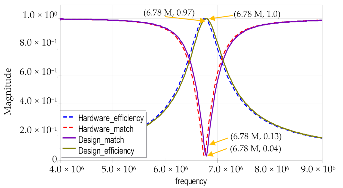
Figure 11 shows the efficiency and impedance matching of the designed coupler and the fabricated hardware coupler. In terms of both efficiency and impedance matching, the fabricated hardware agrees with the designed coupler.
Figure 11 indicates that the efficiency of the designed coupler is 1, whereas the hardware varies by 2%, which equals 0.98. The ideal value for the impedance matching of S-CPT is 0; however, the obtained design and hardware values are 0.03 and 0.13, respectively. Increasing the impedance matching value increases the reflected voltage through the primary side. Consequently, a high impedance matching value increases the loss. Therefore, good S-CPT designs have an impedance matching value close to 0.
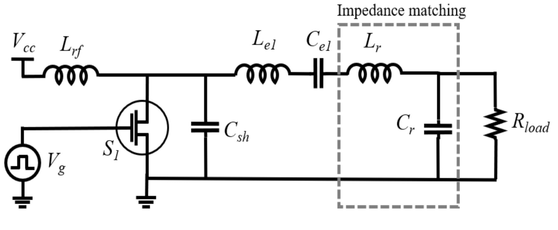
2.2. Class-E Inverter with a Balun
The class-E power amplifier in
Figure 12 was designed with a 10-W S-CPT system, with an operating frequency of 6.78 MHz. Class E was designed using the equations [
23].
Figure 12 presents the components of class E, whereas
Table 4 lists the obtained parameters.
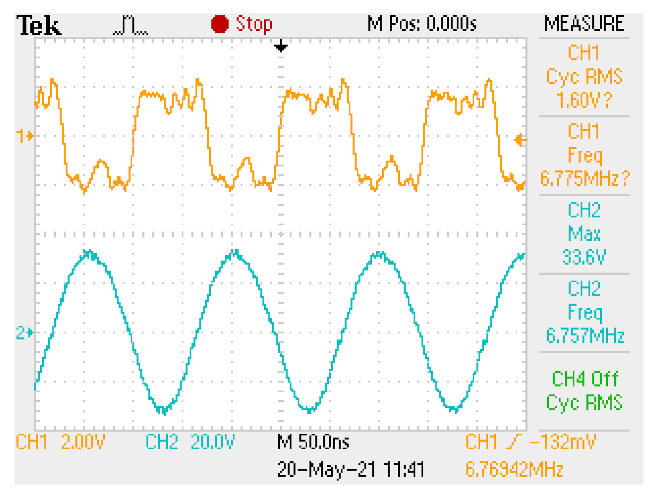
The clock IC drives the voltage signal to the driver of the GanFET during the commuting process.
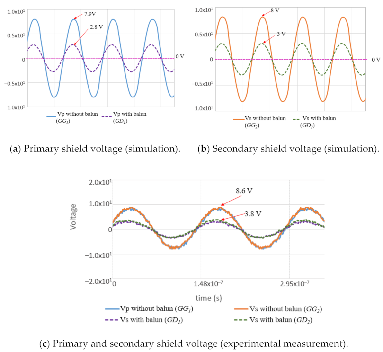
Figure 13 shows the generated clock IC voltage and the output of the class-E inverter. The class-E inverter reached an efficiency of 79% with an output load of 50 Ω.
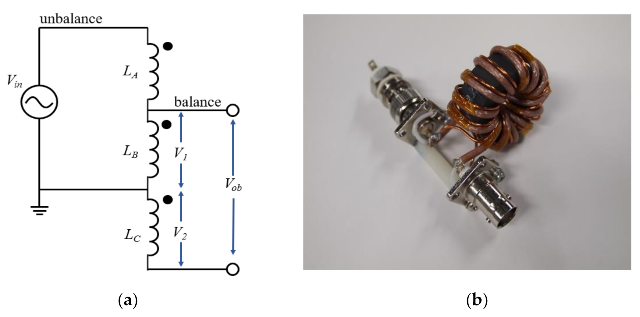
A balun converts a single unbalanced signal into two balanced differential signals [
24]. The Ruthroff-type balun has a lower insertion loss than a transformer type and requires ferrite as the core material to maintain its performance [
25]. A narrow bandwidth moderates the insertion loss of the transformer type owing to its resonance mechanism [
26]. Therefore, the S-CPT system used a Ruthroff 1:1 balun to convert the differential voltage, which was used as input for the CPT system.
Figure 14 shows the Ruthroff balun with two output voltages, and the relationship between the voltage outputs
Vob and output voltage is given in Equations (5) and (6).
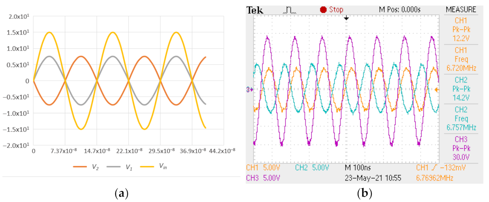
The balun was analysed via both a simulation and an experiment, and
Figure 15a,b presents the results, respectively.
Figure 15a shows the simulated result of the balun with an input amplitude voltage of 15 V. Both the output voltages
V1 and
V2 exhibited an amplitude of 7.5 V. The experimental result in
Figure 15b displays the input amplitude voltage of 15 V, in which the output voltages
V1 and
V2 were 6.1 and 7.1 V, respectively. These results show good agreement between the simulation and hardware values of the balun.
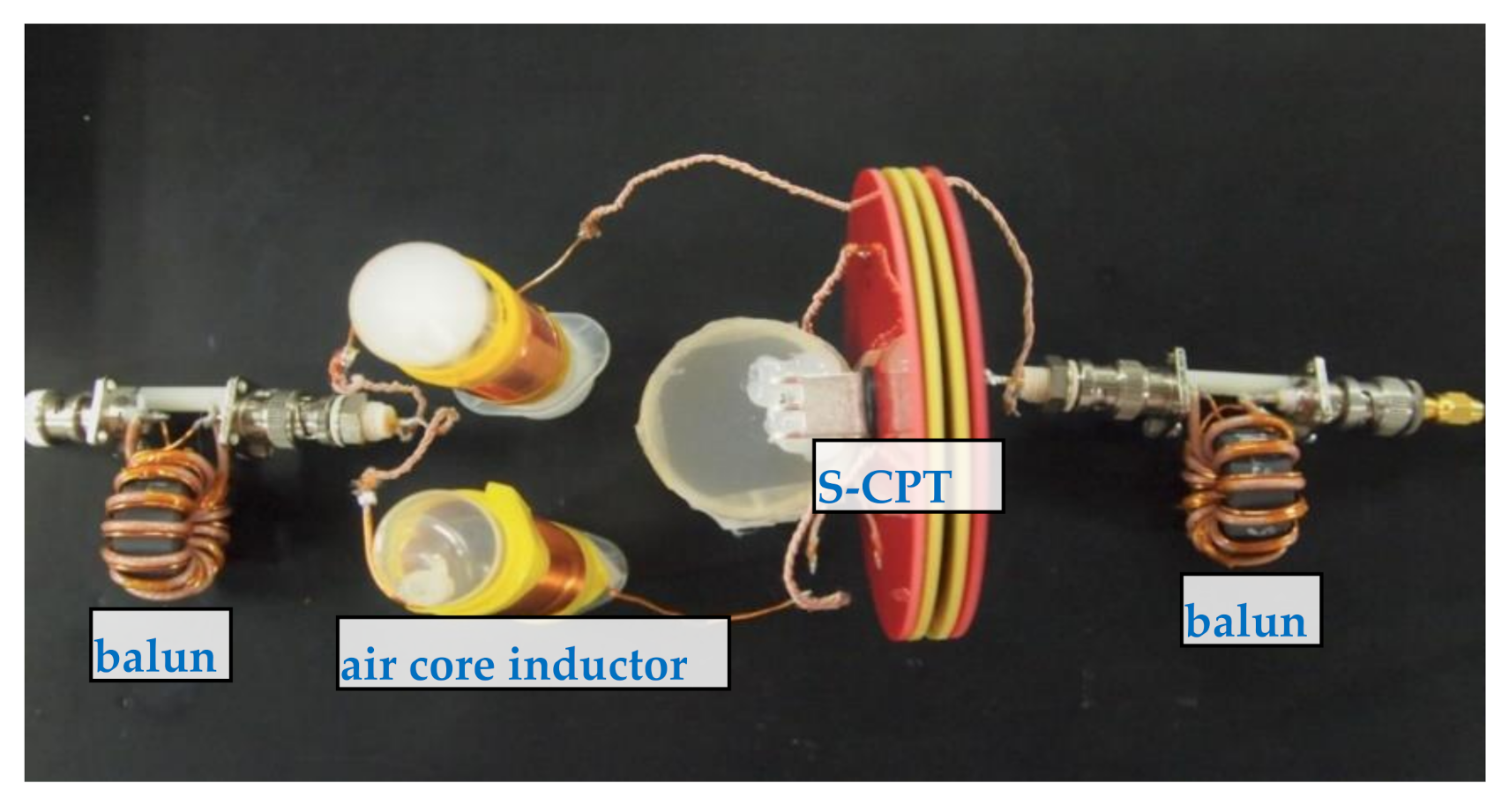
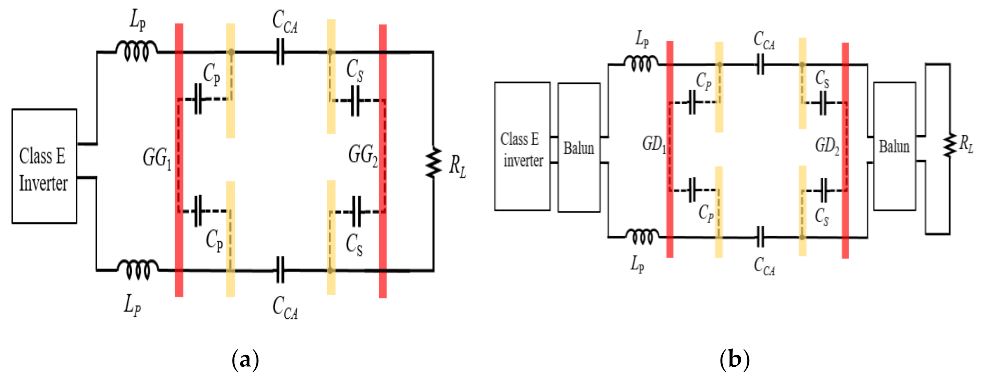
The S-CPT system was set up as shown in
Figure 16a,b to compare the voltage at the shield plate with and without the balun circuit.
Figure 16a shows the connection of the components in the S-CPT system with class E, with the voltage points at the primary and secondary sides represented by
GG1 and
GG2, respectively. The balun is connected to the inductor, and the complete topology is shown in
Figure 16b with the voltage point at the shield plate in the primary part
GD1 and that in the secondary part
GD2.
Figure 17 shows the experimental setup with a balun. A Litz wire connects the balun to the air-core inductor. The coupler was fabricated and measured to meet the closest design value;
Table 1 lists the measured values. The hardware experiment was set up to measure the voltage at the shield for S-CPT without and with the balun, as shown in
Figure 16a,b, respectively.
An LTspice simulation was used to investigate the voltage point in both circuits using a sinusoidal approach to observe and compare both topologies with the simulation results.
Figure 18 shows the simulation and experimental results.


