Article

PWM Strategy to Alleviate Common-Mode Voltage with Minimized Output Harmonic Distortion for Five-Level Cascaded H-Bridge Converters

1
Faculty of Electronics and Electrical Engineering, Ho Chi Minh City University of Technology (HCMUT), 268 Ly Thuong Kiet Street, District 10, Ho Chi Minh City BP 70000, Vietnam
2
Vietnam National University Ho Chi Minh City, Vietnam Linh Trung Ward, Thu Duc District, Ho Chi Minh City BP 70000, Vietnam
3
Faculty of Electrical and Electronics Engineering, Ho Chi Minh City University of Technology and Education, Ho Chi Minh City BP 70000, Vietnam
*
Author to whom correspondence should be addressed.
Energies 2021, 14(15), 4476; https://doi.org/10.3390/en14154476
Submission received: 28 June 2021 / Revised: 19 July 2021 / Accepted: 21 July 2021 / Published: 24 July 2021
(This article belongs to the Section F: Electrical Engineering)

Abstract

:
High-frequency components of common-mode voltage (CMV) induce the shaft voltage and bearing current, which lead to premature failures in motors. In addition, due to non-zero average CMV, the low-frequency components of CMV, particularly the third-order harmonic component, have been reported to cause difficulties in common-mode filter design. Furthermore, the utilization of distant voltage vectors in the pulse-width modulation (PWM) with reduced CMV magnitudes gives rise to high output harmonic distortion compared to PWM ones without CMV reduction. In an attempt to solve the aforementioned issues, this article presents a PWM strategy that features reduced CMV magnitudes, zero average CMV, and improved output harmonic distortion for a five-level cascaded H-bridge (CHB) converter. In addition, the carrier rotation technique based on the phase-leg redundancy of the CHB topology is also combined with the proposed scheme to achieve equal power loss distribution among power switching devices. Both simulation and experimental results confirm that the proposed strategy produces better output harmonic distortion than that of POD-SPWM and APOD-SPWM under the condition of reduced CMV magnitudes, zero average CMV, and equal power loss distribution.

1. Introduction

Multilevel converters have found themselves in many industrial motor-drive applications. Several advantages, when compared to two-level ones, include lower harmonic distortion, higher blocking voltage, a more significant number of redundant switching states, lower electromagnetic interference (EMI), and lower dv/dt [1]. Some prominent multilevel converter topologies are neutral point clamped (NPC), flying capacitor (FC), and cascaded H-bridge (CHB) converters. Among them, CHB converter topologies have been widely used in industrial applications, especially for the number of levels being greater than or equal to 5 (n 5). Aside from inheriting all the strengths of multilevel converters, they also possess some other merits such as a modular structure [2], a smaller number of switching devices as opposed to NPC converter topologies for the same number of levels [3]. With regard to the DC-link voltage levels among different cells in the same phase leg, the CHB converters can be classified as asymmetric and symmetric ones. The asymmetric CHB topologies aim at reducing the number of isolated DC-link voltages required for a given number of voltage levels [4]. The ratio of DC-link voltage levels among different cells in the same phase leg can be binary [5] or trinary [6]. In the binary asymmetric CHB topology [5], the research work further reduces the number of isolated DC-link voltages in a phase leg to one while the remaining DC-link voltages of other cells in the same phase leg are floating and are balanced by a technique called level doubling network. Similarly, the work in [6] proposed a modulation scheme for a trinary asymmetric CHB topology to balance the floating capacitor voltages of the remaining cells by utilizing the redundancies available in the trinary space vector diagram. In general, the unequal DC-link voltages in the asymmetric CHB topologies lead to complicated modulation schemes and uneven power-sharing among different cells. On the contrary, the power loss balance among switching devices can be achieved thanks to phase-leg redundancy in the symmetric CHB converters. This unique feature in the symmetric CHB converters manifests itself in the form of carrier rotation in which numerous research works [7,8,9,10] have utilized to equally distribute power loss among switching devices for a whole modulation range. The underlying principle of the carrier rotation is to rotate the carrier in a cyclic manner, which could be a fundamental modulating cycle [7], a full carrier cycle [8], a half carrier cycle [9], or a quarter of carrier cycle [10]. The choice of carrier-rotation cycle depends upon the modulation schemes and the total time required to achieve power balance [9,10]. In contrast, due to the lack of phase-leg redundancy of an NPC converter, the power loss balance cannot be realized, thereby reducing its reliability in the long run [11]. Moreover, the DC-link capacitor voltage balancing control in the NPC converter is relatively complex for five levels or above (n 5), rendering it unattractive for industrial applications as opposed to the CHB counterpart. The research work in [12] proposed a carrier-overlapped PWM for neutral-point (NP) voltage balancing in a five-level NPC inverter. Despite successfully balancing the NP voltage in a five-level NPC converter, the total harmonic distortion given by the proposed strategy is even inferior to that of the three-level NPC inverter for the modulation range of m 0.6 while using twice the number of switching devices in comparison to the three-level NPC one. The research work in [13] extends the one in [12] for n-level NPC inverters. However, the proposed scheme was applied to a five-level NPC inverter in both simulation and experiment, and the output harmonic distortion is once again higher than that of a three-level NPC one for m 0.6, albeit being capable of balancing the NP voltage.
Despite having the merits mentioned above, CMV still occurs in CHB converters. Large magnitudes and high-frequency components of CMV give rise to shaft voltage and bearing current, thereby leading to premature failures in motors as indicated in [14]. Moreover, in medium-voltage motor-drive applications, high CMV magnitude leads to the destruction of motor insulation [15]. Hence, the magnitude of which must be reduced. Aside from the high-frequency components of CMV, its low-frequency components, especially the third-order harmonic component of CMV, have been reported to cause difficulties in filter design, as well as heated CM inductors as reported in [16]. In an attempt to solve this problem, the zero-average CMV in a sampling period is, therefore, introduced in [16] to suppress the third-order harmonic component of CMV in a two-level converter. In practice, long cables, connected between the converter and the motor, would exacerbate undesired phenomena associated with CMV, as previously mentioned [17]. Therefore, CMV magnitude reduction and zero average CMV in one sampling period must be ensured.
In terms of solutions for CMV reduction, they can be classified as hardware and software solutions. On the hardware front, the research work in [18] proposed a CM filter to attenuate the conducted EMI generated by CMV. In [19], the researchers proposed a passive EMI filter for eliminating bearing current and ground leakage current. In [20], an integrated AC choke, which combines a common-mode and a differential-mode filter, was presented to suppress the adverse effects caused by CMV. However, the hardware solutions increase the cost and volume of a system. On the contrary, software methods only involve modifying PWM strategies. Hence, they are more preferred over the hardware ones.
From the perspective of CMV alleviation, PWM methods can be classified as fully-eliminated-CMV PWM, partially-eliminated-CMV PWM, and non-eliminated-CMV strategies. Under the fully-eliminated-CMV PWM schemes, CMV can be theoretically eliminated to zero by avoiding all switching states that generate CMV magnitudes. Due to having no zero-CMV-magnitude vectors in the two-level space-vector diagram, the complete CMV elimination cannot be achieved in a conventional two-level converter [21] and is only feasible for odd n-level converters. As a result, the research work in [22] proposed a fully-eliminated-CMV strategy in conjunction with switching loss reduction under different power factor conditions for odd n-level converters. The switching loss reduction is realized based on the redundancies of implementation of zero-CMV switching sequences in a carrier period, in which the sequence with double switching commutations is assigned to one of the three phases with maximum absolute current magnitude. However, the total harmonic distortion of the proposed strategy in [22] is significantly higher than that of in-phase disposition sinusoidal PWM (IPD-SPWM) due to the use of distant zero-CMV vectors. The fully-eliminated-CMV scheme proposed in [23] aims to solve the deficiency of high harmonic distortion in [22] by once again utilizing the redundancies of implementation of zero-CMV switching sequences. The analytical harmonic distortion factor then determines which redundancy that leads to minimum harmonic distortion. The research work in [24] further improves the harmonic distortion produced in [23] by modifying the switching sequence in a carrier period. In [25], a marginal improvement of harmonic distortion is observed for a fully-eliminated-CMV PWM strategy with the use of a sawtooth carrier over the one in [24]. Even though the CMV magnitude is theoretically eliminated to zero, the CMV spike still occurs due to the deadtime effect. As a result, the work in [26] was presented to reduce the CMV spike. Nevertheless, the CMV spike is reduced at the expense of high switching loss. Although significant efforts have been made to reduce the harmonic distortion and switching loss in the fully-eliminated-CMV PWM strategies, both harmonic distortion and switching loss are still significantly higher than those of partially-eliminated-CMV PWM and non-eliminated-CMV PWM ones [27], thereby raising the torque pulsation in motors and reducing the overall efficiency of a system. The partially-eliminated-CMV schemes offer a nice balance among the CMV magnitude reduction, the THD of outputs, and the switching loss by neglecting switching states that generate high CMV magnitudes. In the conventional two-level converters, owing to the nonexistence of zero-CMV voltage vectors, significant attention has been paid to reduce the CMV magnitudes by avoiding the two zero voltage vectors. Several PWM strategies include remote state PWM (RSPWM) [28], active zero-state PWM (AZPWM) [29], and near state PWM (NSPWM) [30]. A comparative analysis of harmonic distortion for the above-mentioned PWM strategies is included in [31]. As demonstrated in [31], a common drawback of these strategies is the deteriorated output quality compared to the non-eliminated-CMV strategy such as SPWM. Therefore, the demand for both CMV-magnitude reduction and improved output quality gives rise to the adoption of multilevel converters. Owing to the complex control of NP voltage balancing for n 5 and uneven power loss distribution in an NPC converter, a CHB converter topology is generally preferred.
The partially-eliminated-CMV PWM strategy typically used in a CHB converter is phase opposition disposition SPWM (POD-SPWM), whereas the non-eliminated-CMV-PWM ones are IPD-SPWM and alternate phase opposition disposition SPWM (APOD-SPWM). Regarding the output quality, as demonstrated in [32], IPD-SPWM produces the best output harmonic distortion performance compared to APOD-SPWM and POD-SPWM due to the use of three nearest vectors. Unfortunately, the CMV magnitude given by IPD-SPWM is twice as high as that of POD-SPWM. Although the CMV magnitude reduction is achieved in POD-SPWM, its total harmonic distortion is noticeably higher than IPD-SPWM, as indicated in [32].
As a result, this article presents a PWM strategy with reduced CMV magnitude and zero average CMV in conjunction with minimized output harmonic distortion for a five-level CHB converter. The key contributions of the article include:
(1)
A PWM strategy featuring reduced CMV magnitudes, zero average CMV, and minimum output harmonic distortion is extended from a three-level NPC [33] to a five-level CHB converter;
(2)
A carrier-rotation technique [7] is combined with the proposed scheme for even power loss distribution in a five-level CHB converter, thereby enhancing the efficiency and reliability over the long term compared to a five-level NPC one;
(3)
A power loss analysis conducted in a PLECS thermal module is presented to confirm the even distribution of power loss, and to establish the condition of equivalent switching loss power under which the harmonic distortion of different PWM strategies is fairly compared against one another;
(4)
A detailed comparative analysis of output harmonic distortion on the basis of comparable switching loss power is conducted in both simulation and experiment for the proposed strategy, POD-SPWM, APOD-SPWM, and IPD-SPWM.
Finally, the article is organized as follows: Section 2.1 presents a mathematical model of a five-level CHB converter for a seamless extension of the proposed PWM strategy. Section 2.2 further enhances the performance of the proposed one by employing the carrier-rotation technique unique to a CHB topology for even power loss distribution. Section 3 illustrates some fundamental performance criteria for evaluating any PWM strategy, such as power loss (conduction and switching loss), total harmonic distortion, weighted total harmonic distortion, and RMS value of phase current ripple. Section 4 details a comparative analysis of output harmonic distortion, CMV magnitudes, and power loss in the simulation for the proposed one, POD-SPWM, APOD-SPWM, and IPD-SPWM. Section 5 demonstrates a comparative analysis of harmonic distortion in the experiment for the strategies mentioned above. Section 6 includes key remarks on the performance of the proposed scheme over POD-SPWM, APOD-SPWM, and IPD-SPWM.

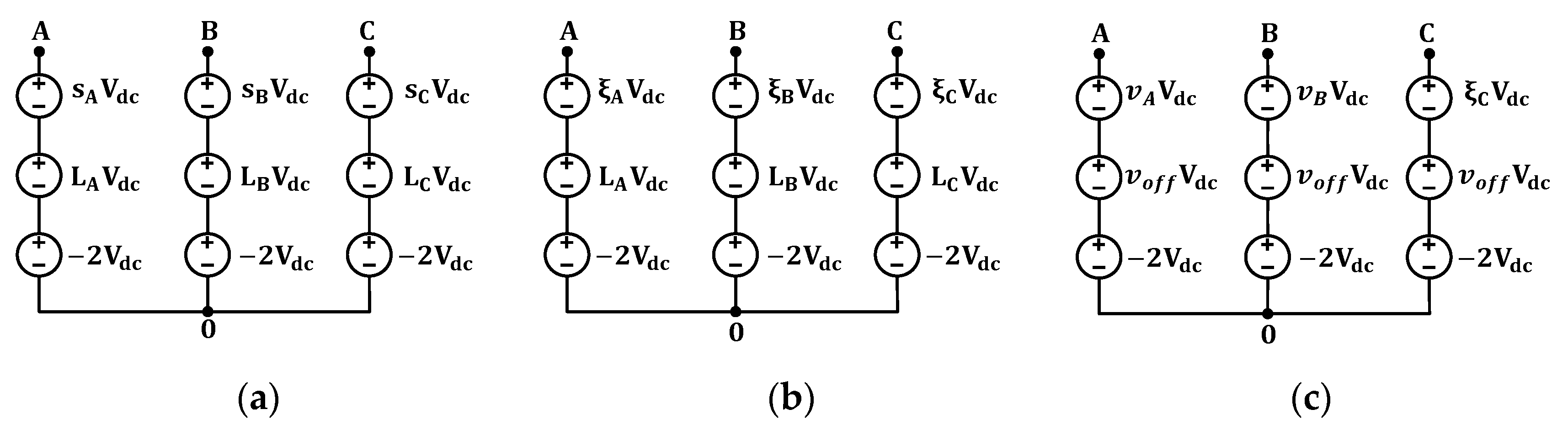
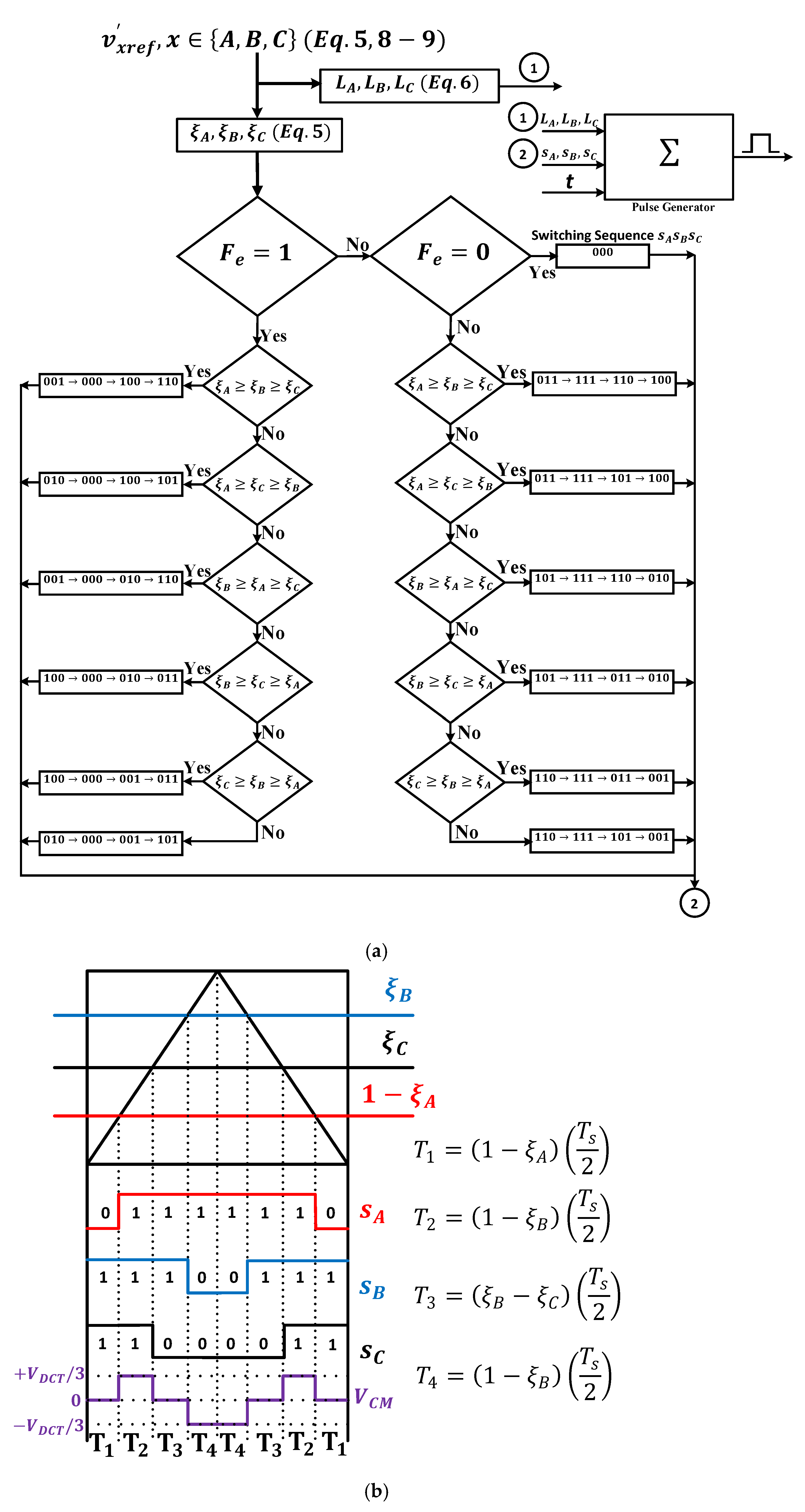
2. PWM Strategy to Alleviate CMV with Improved Output Harmonic Distortion and Equal Loss Distribution

2.1. With CMV Alleviation and Improved Output Harmonic Distortion

This section presents a PWM method for CMV alleviation, which can be achieved by reducing CMV magnitudes and maintaining zero average CMV in one sampling period. In addition, the output harmonic distortion is also minimized, thereby enhancing the overall efficiency of a system.
The PWM strategy for a 5-level CHB converter is derived based upon the equal DC-link voltage condition, which can be obtained by multi-pulse diode rectifiers [1]. Hence, the instantaneous pole voltages of phase leg A ( V A O ), phase leg B ( V B O ), and phase leg C ( V C O ) as shown in Figure 1a can be expressed as:
V A O = ( S 1 A + S 2 A + S 3 A + S 4 A ) × V d c 2 V d c
V B O = ( S 1 B + S 2 B + S 3 B + S 4 B ) × V d c 2 V d c
V C O = ( S 1 C + S 2 C + S 3 C + S 4 C ) × V d c 2 V d c
where S i x , i { 1 , 2 , 3 , 4 }   x { A , B , C } is regarded as a switching state of SWix, which assumes a value of 0 or 1.
The virtual instantaneous normalized switching voltage of phase leg A ( V A N ), phase leg B ( V B N ), and phase leg C ( V C N ) can then be written as:
V A N = ( S 1 A + S 2 A + S 3 A + S 4 A ) , 0 V A N 4
V B N = ( S 1 B + S 2 B + S 3 B + S 4 B ) , 0 V B N 4
V C N = ( S 1 C + S 2 C + S 3 C + S 4 C ) , 0 V C N 4
As for 5-level NPC converters, there is a restriction over the switching states constituting the normalized switching voltage V x N , i.e., S 1 x S 2 x S 3 x S 4 x [22]. However, there is no such restriction in 5-level CHB converters. This characteristic is referred to as phase-leg redundancy on which the carrier-rotation techniques [7,8,9,10] are based to distribute the power loss among switching devices equally.
The instantaneous normalized switching voltage of phase leg A ( V A N ) in (4), phase leg B ( V B N ) in (5), and phase leg C ( V C N ) in (6) can be decoupled into 2 components.
V A N = s A + L A
V B N = s B + L B
V C N = s C + L C
where s x is the active switching state of phase leg x { A , B , C } which takes a value of 0 or 1. L x is the base voltage of phase leg x { A , B , C } .
The instantaneous CMV can be defined as [22,23,24,25,26]:
V C M = ( V A O + V B O + V C O ) 3 = ( V A N + V B N + V C N 6 V d c ) 3
The average value of V A N , V B N , V C N in one sampling period can be written as:
V A N ¯ = v A r e f = v A r e f + v o f f = ξ A + L A
V B N ¯ = v B r e f = v B r e f + v o f f = ξ B + L B
V C N ¯ = v C r e f = v C r e f + v o f f = ξ C + L C
L A = { I n t ( v A r e f ) , v A r e f < 4 3 ,   v A r e f = 4
L B = { I n t ( v B r e f ) , v B r e f < 4 3 ,   v B r e f = 4
L C = { I n t ( v C r e f ) , v C r e f < 4 3 ,   v C r e f = 4
where v x r e f is the reference voltage signal of phase x { A , B , C } .
v o f f is the offset voltage.
ξ x is the average active switching state of phase x { A , B , C } .
L x is the base voltage of phase x { A , B , C } . and I n t ( v x r e f ) returns the smallest integer value of v x r e f .
For ease of understanding, the instantaneous, and average voltage models of three-phase legs are illustrated in Figure 2.
The average CMV in one sampling period can be then written as:
V C M ¯ = v C M = ( v A O + v B O + v C O ) 3 = ( v A r e f + v B r e f + v C r e f + 3 v o f f 6 ) V d c 3
The three-phase reference voltage signals in (5) can be expressed as:
v A r e f = 2 m 3 × cos ( ω t )
v B r e f = 2 m 3 × cos ( ω t 2 π 3 )
v C r e f = 2 m 3 × cos ( ω t 4 π 3 )
The condition of zero average CMV dictates the limit of linear modulation region, i.e., 0 m 3 2 . This condition also leads to v o f f in (17) being equal to 2.
Let us define F T , F e , and F L as total switching voltage, total average active switching voltage, and total base voltage, respectively.
F T = F e + F L
F e = ξ A + ξ B + ξ C
F L = L A + L B + L C
The zero average CMV in one sampling period results in F T = 6 in (21). Figure 1b shows that the red-line hexagon is the region where the average CMV is zero. This region consists of six sub-regions corresponding to two cases of F L = 4 and F L = 5 , as shown in Figure 3. The reference vector v r e f in the five-level space vector diagram can be synthesized by ξ r e f in the two-level one with the aid of the base voltage vector L , as illustrated in Figure 1b. Under the condition of zero average CMV and reduced CMV magnitude, three possible switching sequences can be used to synthesize ξ r e f , as shown in Figure 3b, for F L = 4 and ξ r e f in the area (1). Among these, there is only one switching sequence that yields the best output harmonic distortion, i.e., 011 111 110 100 110 111 011 [33]. The dwell time calculation of which is also shown in Figure 4b, along with the flowchart featuring switching sequences for the areas (1)–(6) which also gives the minimum output harmonic distortion. In this article, they are referred to as RCMV1-PWM.

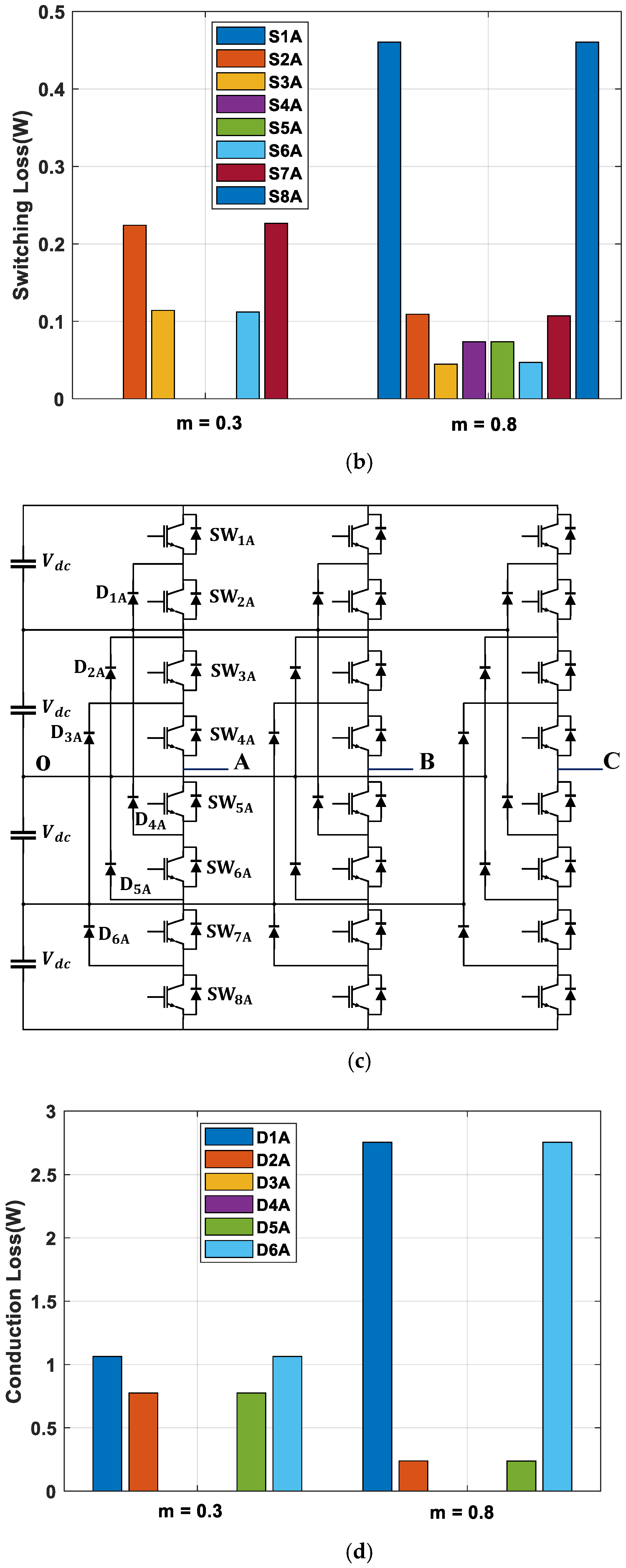
2.2. With Equal Loss Distribution

The presented RCMV1-PWM strategy ensures the zero average CMV, reduced CMV magnitude, and minimum output harmonic distortion. In addition to those, equal power loss distribution among switching devices is also realized by cyclically changing the switching states after a fundamental period of T 0 as per Table 1. In the latter section, RCMV1-PWM is evaluated thoroughly against other methods to confirm the equal distribution of power loss indicated in this section.

3. Performance Criteria for Evaluation

This section presents two important criteria, including the power loss and the harmonic distortion, to evaluate PWM strategies. The power loss estimation is used to verify the power loss balance of the proposed strategy among switching devices, as mentioned in the previous section. In addition, it establishes the condition of comparable power loss on which the harmonic distortion calculation is based to fairly compare across different PWM strategies.

3.1. Power Loss

The power loss, which typically consists of the conduction and switching loss, can be readily estimated by the thermal module in the PLECS simulation program [34]. The principle of power loss calculation is explained in detail in [35]. The power switching devices (IGBTs) with an antiparallel diode used in the five-level CHB inverter are IKW15N120H3, of which the thermal characteristics can be obtained from the manufacturer’s website [36] and imported into the thermal module. For comparison, the power loss distribution of a five-level NPC inverter is also included. The power switching devices IGBTs used in the five-level NPC topology are the same as those in the five-level CHB one and the clamping diode type is IDP30E120, of which the datasheet and thermal characteristics can be found in [37]. For easy reference, some main parameters of IGBT IKW15N120H3 and clamping diode IPD30E120 are tabulated in Table 2 and Table 3.

3.2. Harmonic Distortion

The harmonic distortion performance of each PWM strategy is evaluated by the THD of the voltage and current outputs, the weighted THD (WTHD) of the voltage output, and the root mean square (RMS) of current ripple in Ampere. The formulas of these performance metrics are given as follows [33]:
T H D V L = 1 V m L n = 2 V n L 2
W T H D V L = 1 V m L n = 2 ( V n L n ) 2
T H D I = 1 I m n = 2 I n 2
RMS   current   ripple = 1 T 0 0 T 0 ( i m e s i f u n d ) 2
where: V m L and V n L are the fundamental magnitude and the nth harmonic magnitude of line voltage output, respectively. I m and I n are the fundamental magnitude and the nth harmonic magnitude of phase current output, respectively. I m e s and I f u n d are the measured and the fundamental component of phase current, respectively.

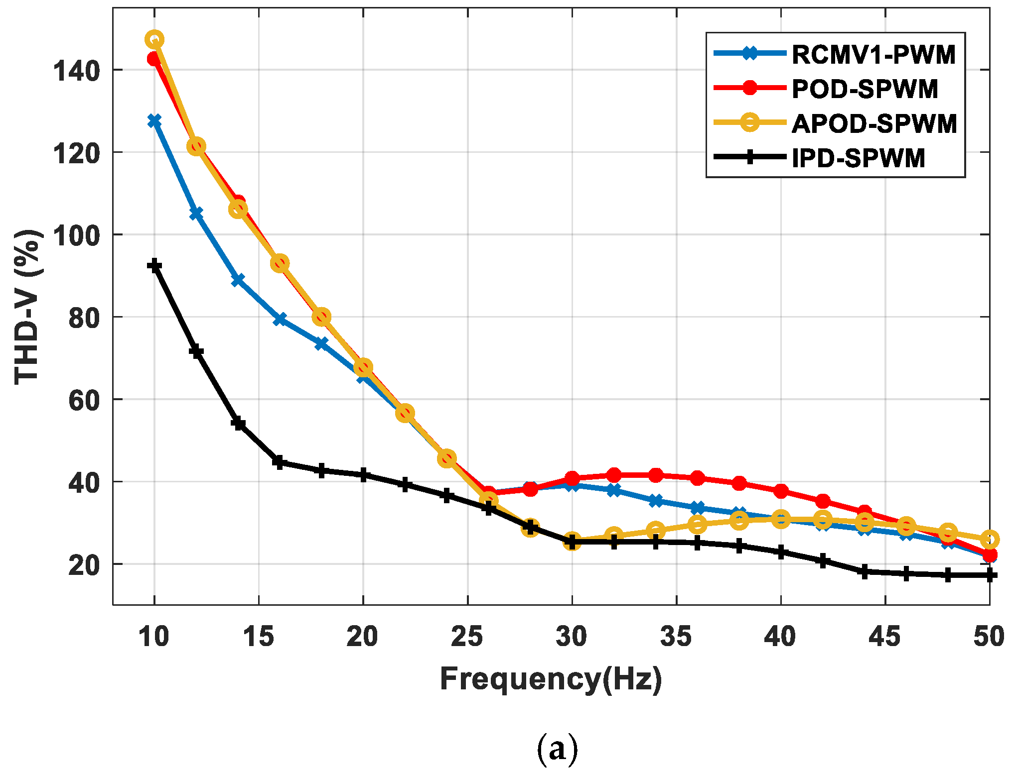
4. Simulation Results

The simulation is conducted in MATLAB/Simulink environment under the condition of V d c = 200   V , f 0 = 50   Hz , f c a r r i e r = 5   KHz , R a = R b = R c = 33.3   Ω , L a = L b = L c = 2.7   mH , C = 4700   μ F for a five-level CHB converter. The comparative analysis of RCMV1-PWM will be conducted against POD-SPWM, APOD-SPWM, and IPD-SPWM in terms of the performance criteria presented in the previous section.

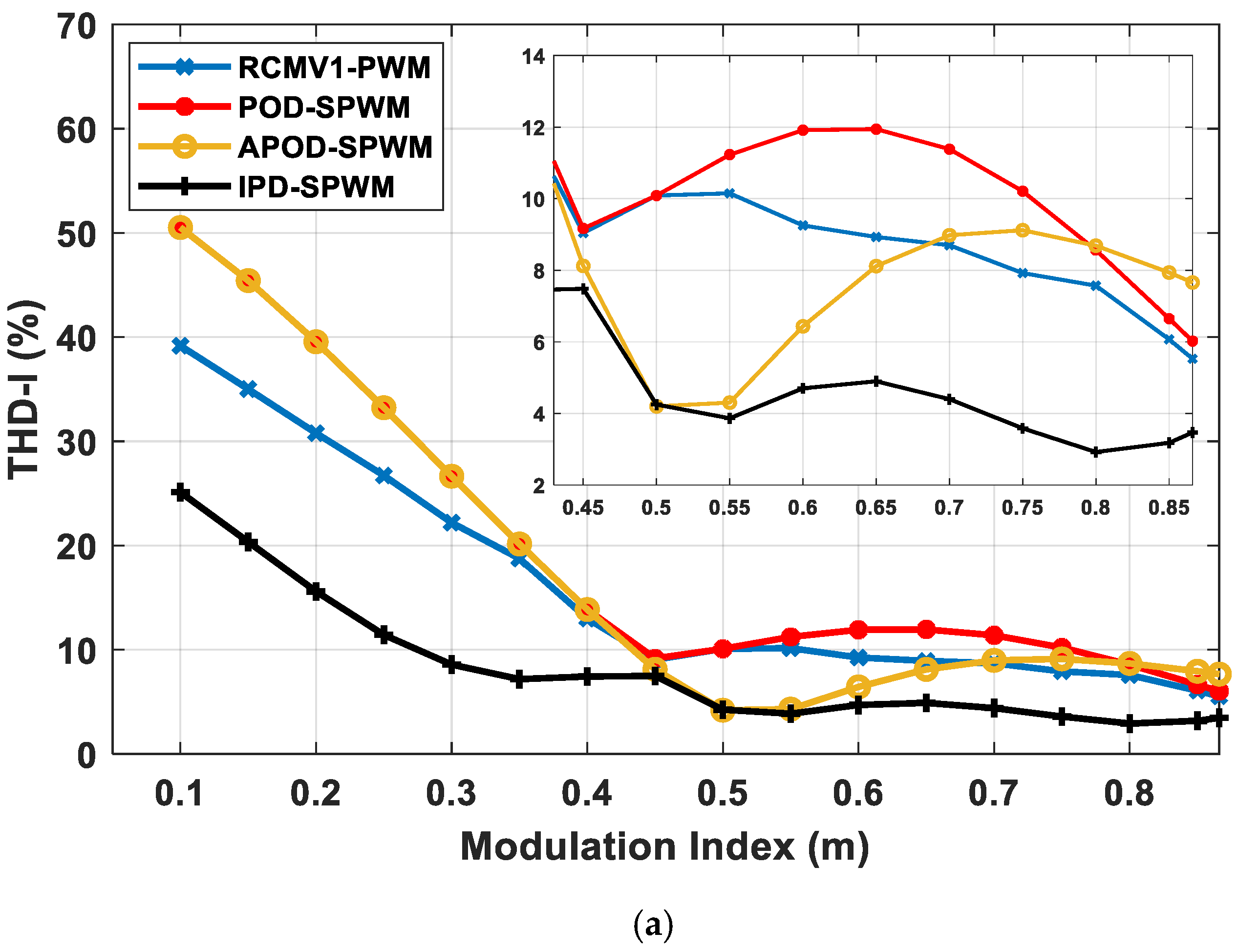
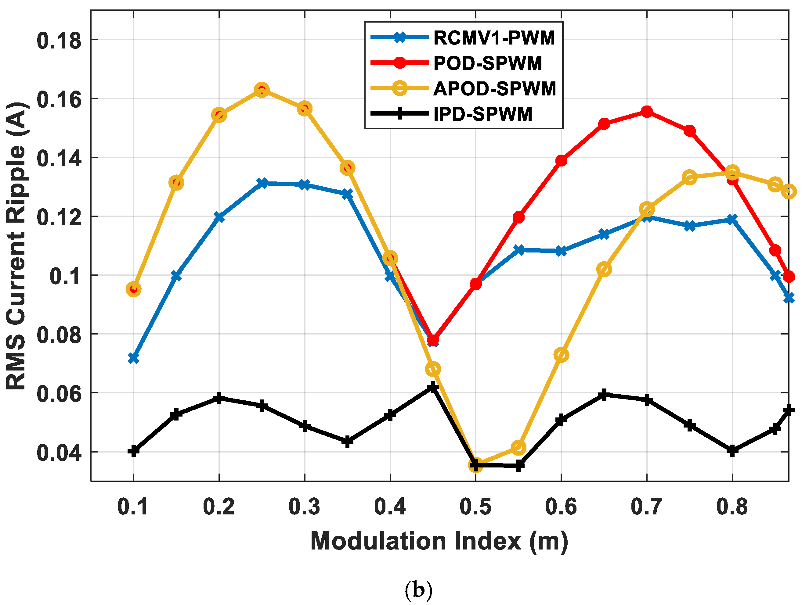
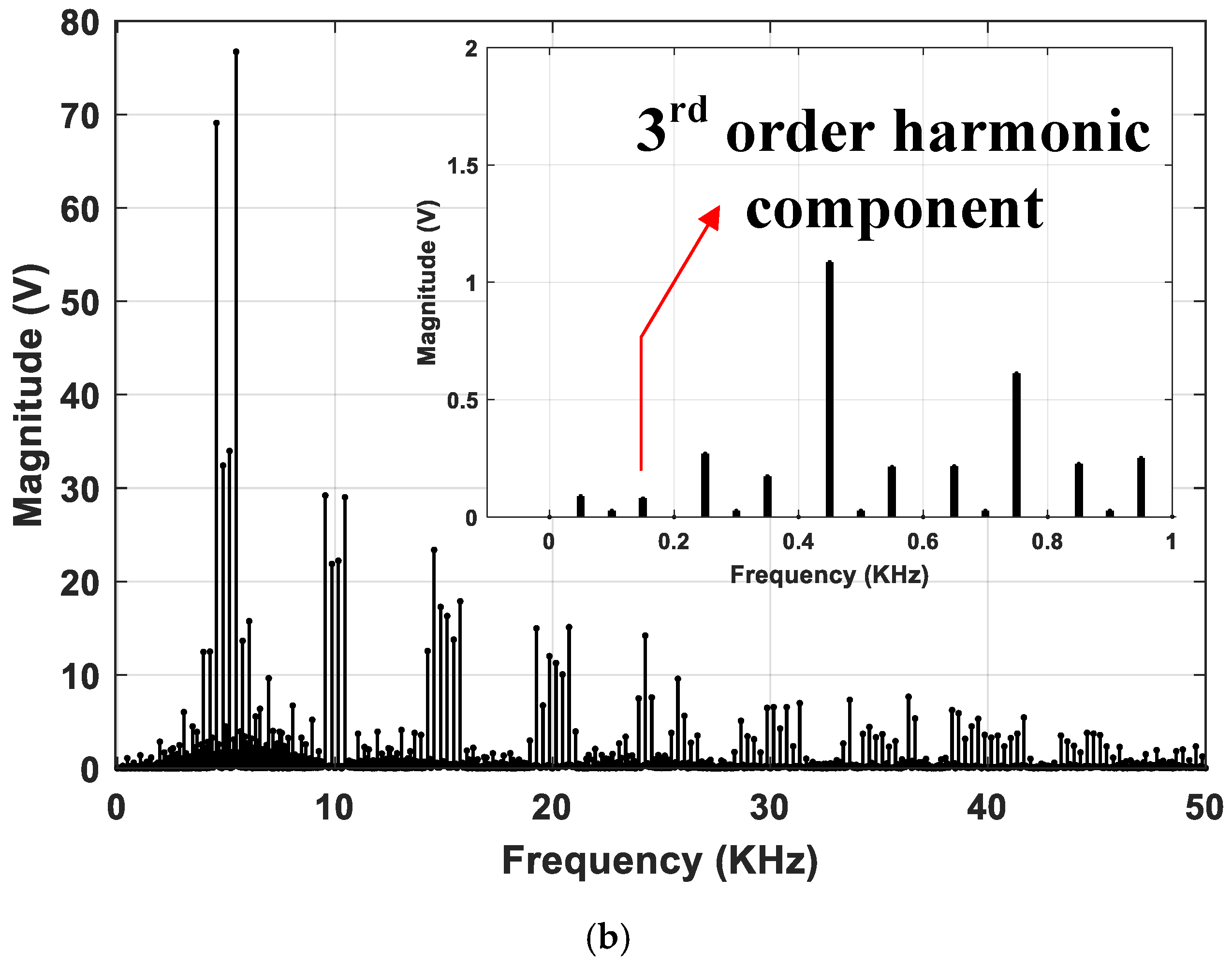
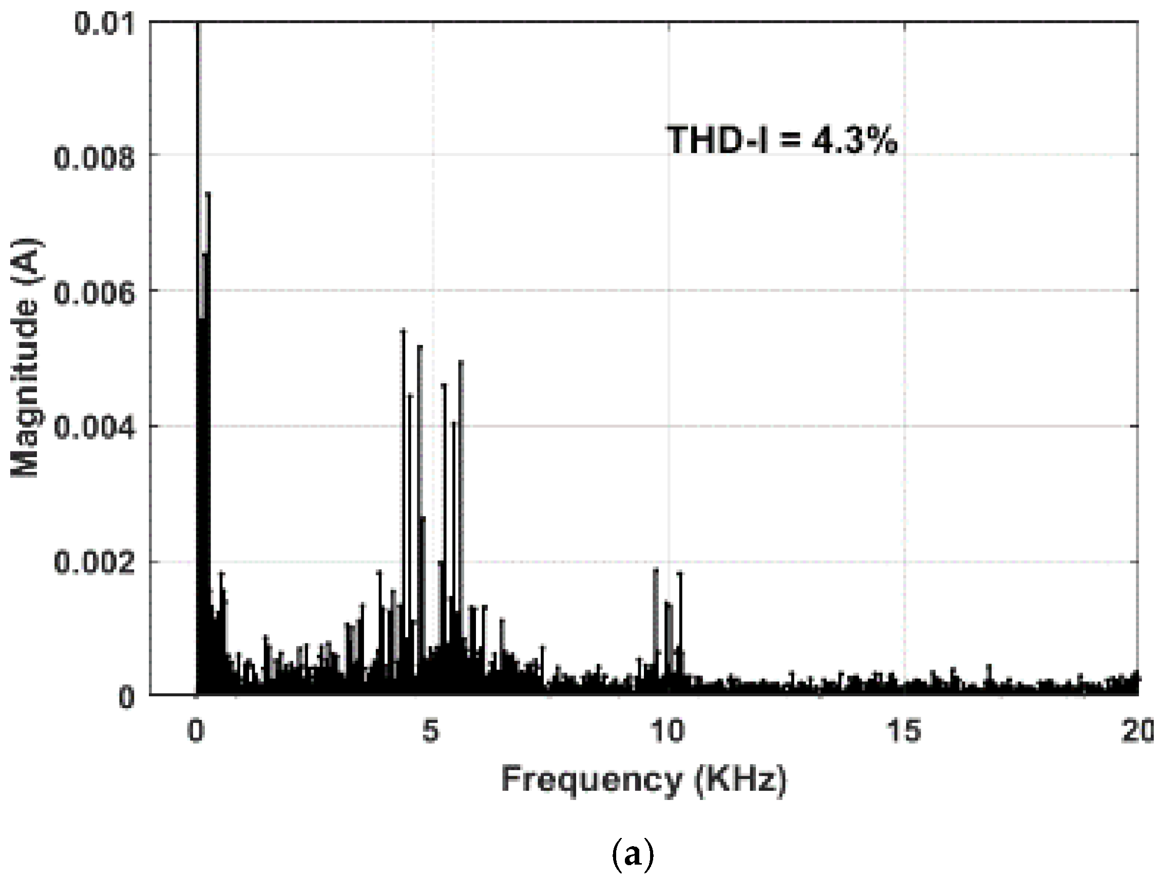
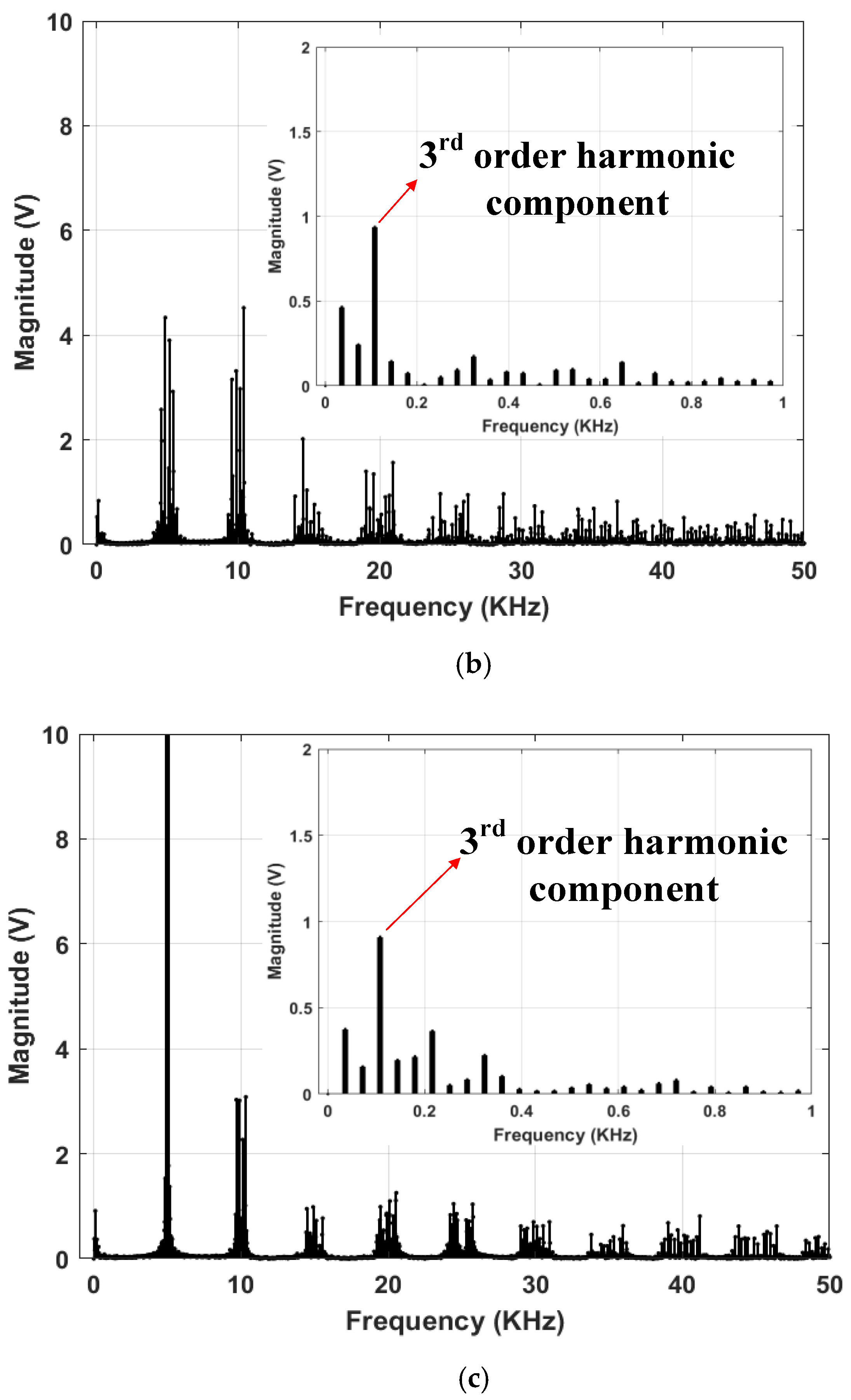
4.1. Harmonic Distortion Evaluation

On the basis of the comparable power loss set forth in Section 4.2, the output harmonic distortion performance of RCMV1-PWM is compared against that of other methods. The THD and WTHD of voltage and the THD of current, as well as the RMS value of current ripple, are evaluated with regard to the modulation index for four strategies. Figure 5 and Figure 6 shows that the IPD-SPWM gives the best output quality for a whole modulation range due to the three nearest vectors principle. However, the magnitude of CMV is twice as high as that of other strategies, as illustrated in Figure 7a. Hence, it is unfavorable in motor-drive applications due to adverse effects of high CMV magnitude, as mentioned earlier. As demonstrated in Figure 5 and Figure 6, the proposed RCMV1-PWM produces better output harmonic performance than the POD-SPWM over a whole modulation range. For example, at m = 0.3, the THD values of voltage and current outputs are 61.78% and 22.19%, respectively, for RCMV1-PWM as opposed to 73.55% and 26.65%, respectively, for POD-SPWM. This translates to a more than 10% improvement of THD of voltage output and a more than 4% improvement of THD of current output. Likewise, at m = 0.3, the WTHD of voltage output, and the RMS value of phase current ripple, are 0.61% and 0.13 A, respectively, for RCMV1-PWM in comparison to 0.73% and 0.16 A, respectively, for POD-SPWM. Both RCMV1-PWM and POD-SPWM produce a reduced magnitude of CMV of V d c / 3 for a whole modulation range, as shown in Figure 7a. As a result, under the reduced-CMV-magnitude condition, RCMV1-PWM is more favorable than POD-SPWM in motor-drive applications due to the lower output harmonic distortion. As for APOD-SPWM, its THD and WTHD of both voltage and current outputs, as well as RMS value of current ripple, are inferior to those of RCMV1-PWM for m 0.45 and m 0.7 . For these two modulation ranges, both APOD-SPWM and RCMV1-PWM obtain a reduced CMV magnitude of V d c / 3 as demonstrated in Figure 7a. For 0.45 m 0.7 , the output harmonic performance of APOD-SPWM is better than that of RCMV1-PWM. However, the CMV magnitude of APOD-SPWM in this modulation range is the same as that of IPD-SPWM, i.e., 2 V d c / 3 as shown in Figure 7a. Hence, the better output harmonic performance of APOD-SPWM is achieved at the expense of higher CMV magnitude. Therefore, under the reduced-CMV-magnitude condition, the proposed RCMV1-PWM gives the most optimum output harmonic performance.
The frequency spectrum of CMV for RCMV1-PWM is also shown in Figure 7b. As can be observed from this figure, the third harmonic component of the CMV ( f 0 = 150   Hz ) is virtually nonexistent, which indicates the zero average CMV in one sampling period is maintained.

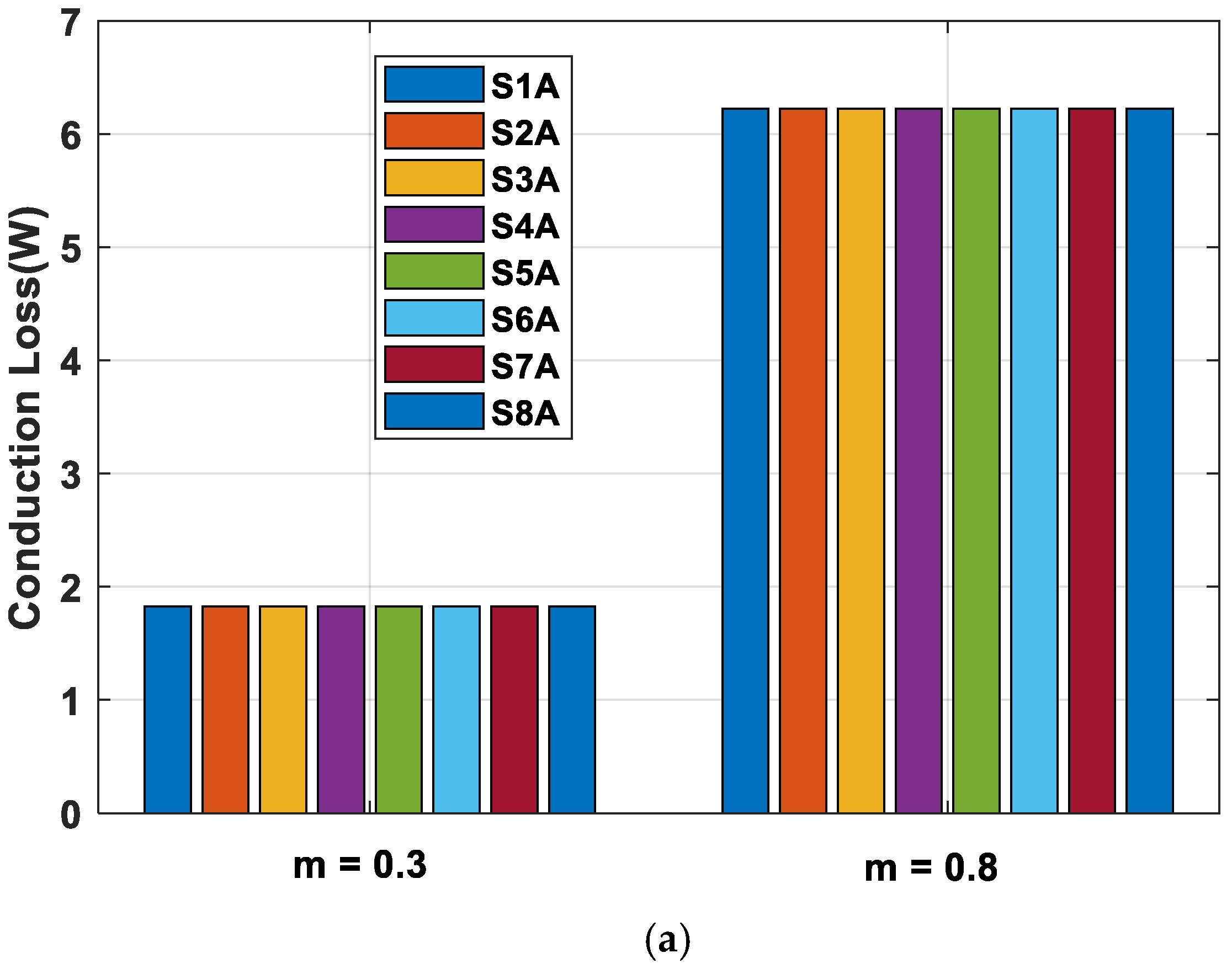
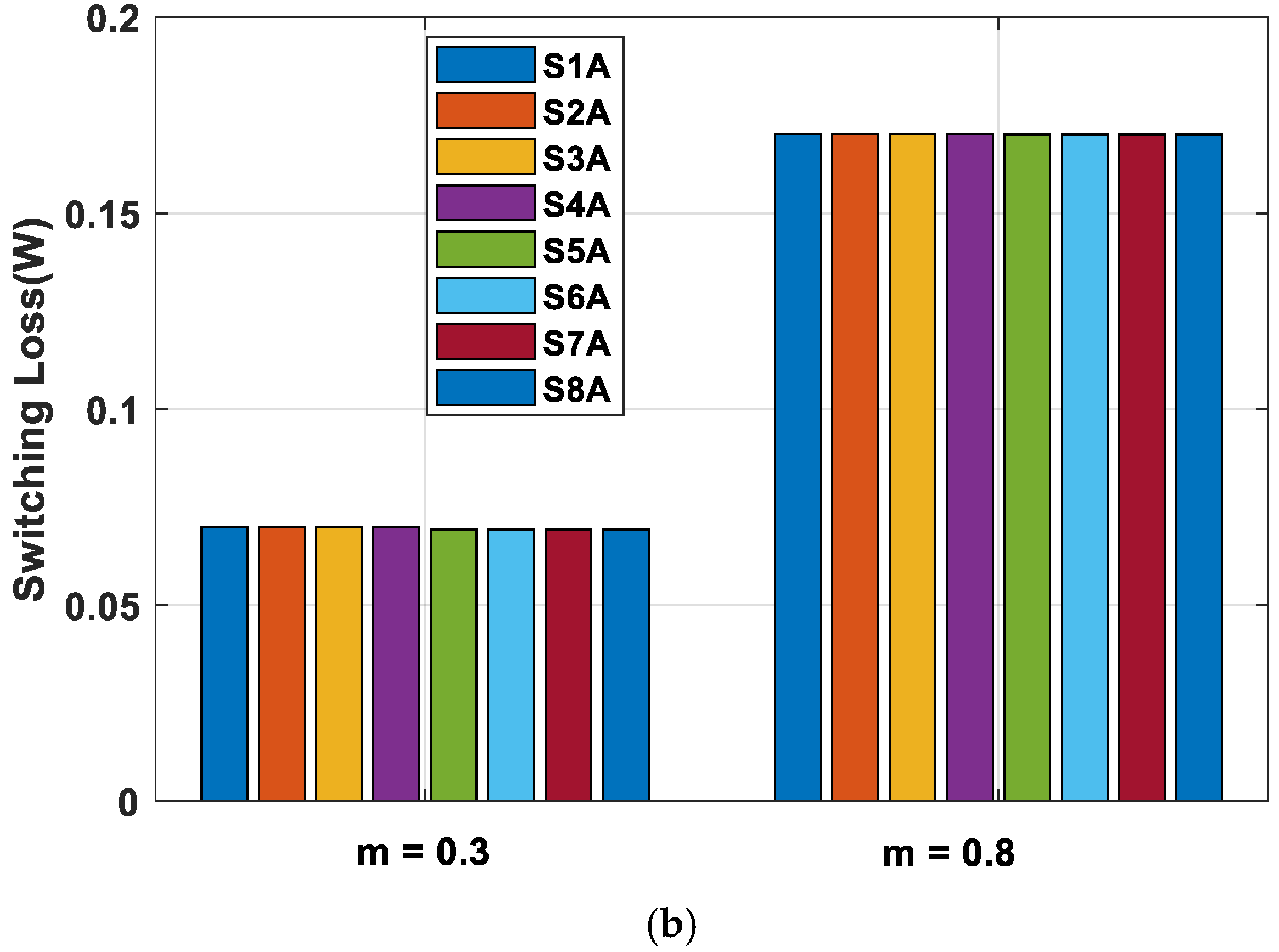
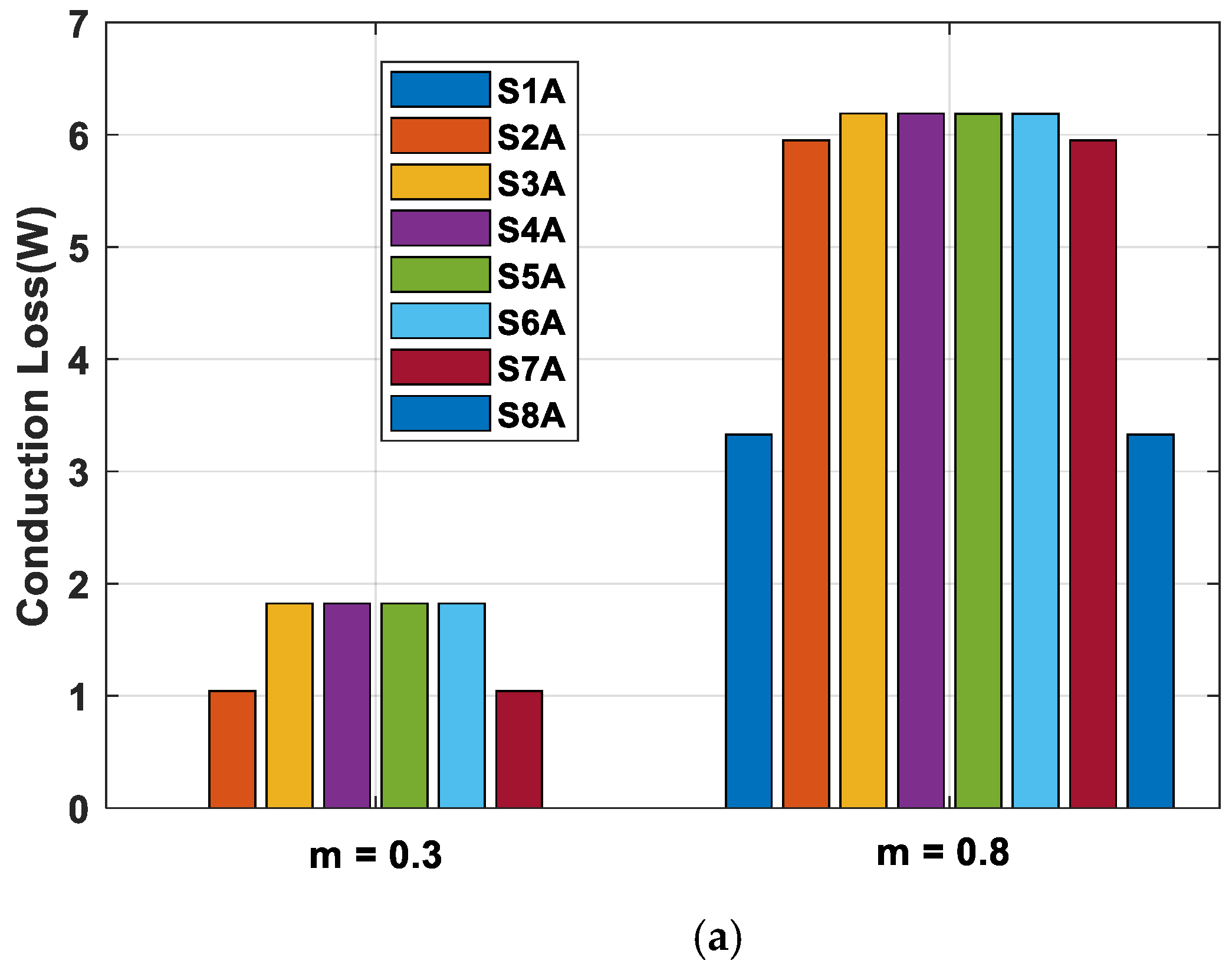
4.2. Power Loss Comparison

The conduction and switching loss of eight IGBTs of the phase leg A for RCMV1-PWM at m = 0.3 and m = 0.8 under the power factor of 0.99 in the five-level CHB inverter are shown in Figure 8. As shown in Figure 8, the equal power loss distribution among switching devices is achieved for the proposed strategy, as indicated in Section 2.
By contrast, the NPC converter, which has the issue of unequal power loss distribution [11] illustrated in Figure 9 for a five-level NPC inverter, possibly leads to failures in some switching devices that have to experience a considerable amount of power loss over a long-term operation, thereby reducing the efficiency and reliability of a system, as well as the overall switch utilization [11]. The active neutral point clamped (ANPC) converter was proposed in [11] to resolve this issue. However, the increase in the number of switching devices results in higher power loss, and the control strategy is more complicated when compared to the CHB converter at the same number of levels. Therefore, the CHB converter topology with the proposed strategy featuring lower CMV magnitude, zero average CMV, and improved output harmonic distortion, as well as equal power loss distribution among switching devices, becomes a topology of choice due to higher efficiency and reliability over a long-term operation as opposed to the NPC one for the number of levels being greater than or equal to 5 (n 5).
In order to further evaluate the power loss performance of RCMV1-PWM, the comparison of its power loss is made against that of POD-SPWM, APOD-SPWM, and IPD-SPWM at m = 0.2, 0.5, and 0.8, as illustrated in Figure 10. As can be seen from Figure 10, both the total switching loss and the total conduction loss of RCMV1-PWM are equivalent to those of other strategies at three modulation indices.

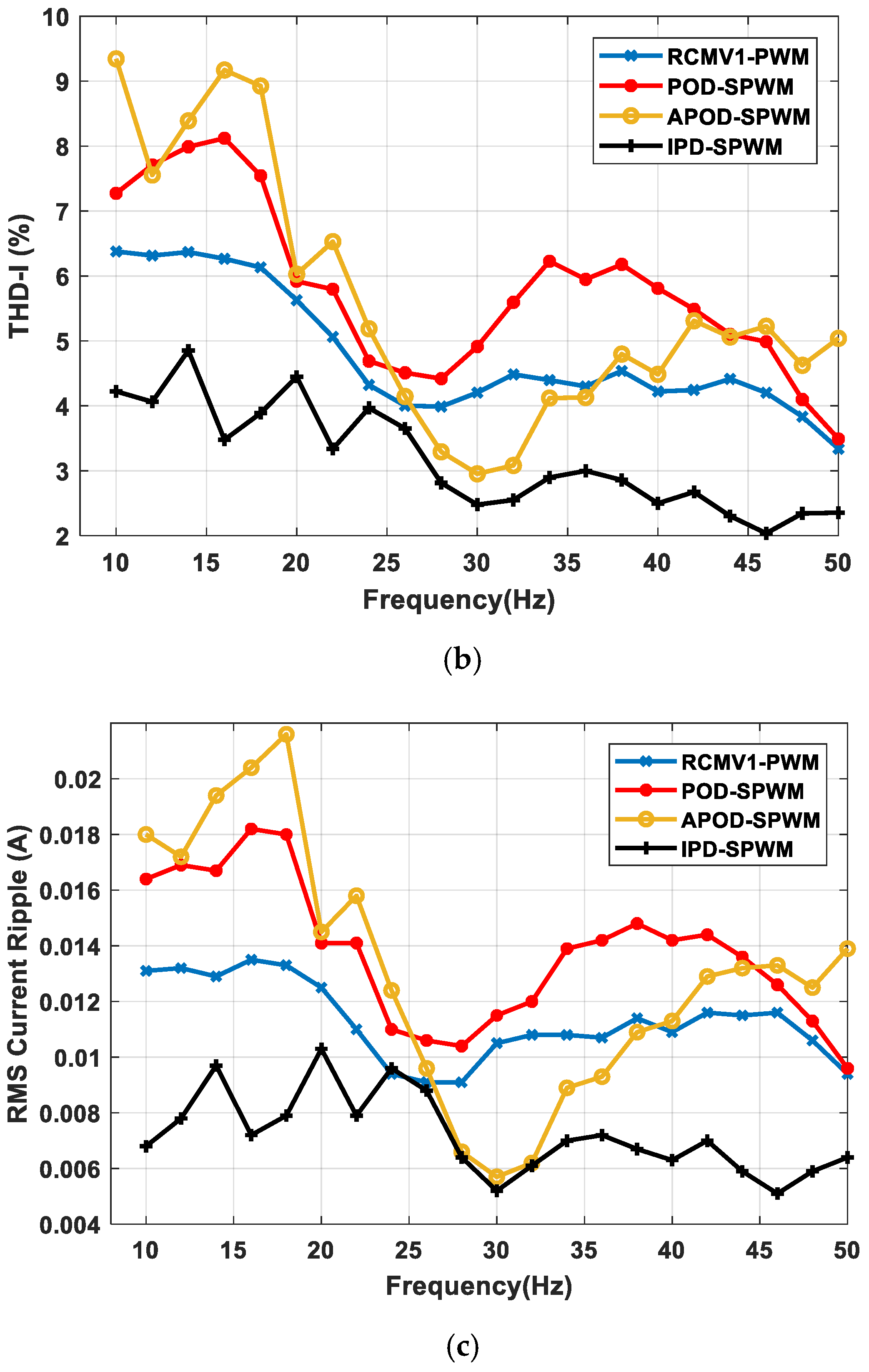
5. Experimental Results

The experiment is conducted on a five-level CHB converter with a no-load three-phase induction motor under the condition of V d c = 50   V , C = 4700   μ F , f c a r r i e r = 5   KHz , f 0 = 50   Hz , deadtime = 2 μ s . The parameters of the three-phase induction motor are as follows: 1.49 KW, 380 V r m s , 50 Hz, Y-connected, R s = 8.68   Ω , R r = 8.3   Ω , L l s = 17.5   mH , L l r = 17.5   mH , L m = 0.862   H . The V/f control is used such that the maximum linear modulation index m = 0.866 corresponds to the rated frequency of 50 Hz. The microcontroller, TMS320F28377D, has been used to fire the gating signals for the switching devices in the five-level CHB converter.
The experimental line voltage and the phase current, as well as the common-mode voltage waveforms, are shown in Figure 11a–c, respectively, for RCMV1-PWM, POD-SPWM, and APOD-SPWM at f0 = 36 Hz (m = 0.623) under the no-load condition. In addition, to demonstrate the output harmonic distortion performance, the experimental THD of line voltage, and the phase current, as well as the RMS values of phase current ripple of RCMV1-PWM, are compared against those of other strategies. As can be observed from Figure 12a, the THD of line voltage of RCMV1-PWM is better than that of POD-SPWM for a whole fundamental frequency range. This is consistent with the simulated one, as shown in Figure 8a. The most noticeable reduction in THD of voltage happens at f0 = 14 Hz, at which it is 88.9% for RCMV1-PWM, as opposed to 106.1% for POD-SPWM. These results in an 18.87% improvement of THD of voltage for RCMV1-PWM over POD-SPWM. The frequency spectra of line voltage at f0 = 36 Hz are shown in Figure 13a,b to further illustrate the THD reduction in line voltage of RCMV1-PWM over POD-SPWM. As can be observed from Figure 13a,b, the harmonic components around the switching frequency (f = 5 KHz) of RCMV1-PWM are significantly less than those of POD-SPWM. In particular, they are less than 14 V in RCMV1-PWM as opposed to more than 25 V in POD-SPWM. With regard to APOD-SPWM, the THD of voltage of RCMV1-PWM is lower than that of APOD-SPWM for f0 < 26 Hz (m < 0.45) and f0 > 40 Hz (m > 0.69). The most significant improvement of the THD of line voltage happens at f0 = 10 Hz, at which it is 127.59% for RCMV1-PWM compared to 147.32% for APOD-SPWM. This translates to a 19.72% improvement of the THD of the voltage of RCMV1-PWM over APOD-SPWM. For 26   Hz f 0 40   Hz , the THD value of the voltage of APOD-SPWM is better than that of RCMV1-PWM. However, this frequency range 26   Hz f 0 40   Hz ( 0.45 m 0.69 ) coincides with the higher CMV magnitude ( 2 V d c / 3 ) of APOD-SPWM than that ( V d c / 3 ) of RCMV1-PWM and POD-SPWM, as demonstrated in Figure 10a. As can be observed from Figure 12a, IPD-SPWM still produces the best output harmonic distortion. However, its magnitude of CMV is twice as high as that of RCMV1-PWM and POD-SPWM for a whole frequency range and is the same as that of APOD-SPWM for f 0 26   Hz ( m 0.45 ).
With regard to the current, the THD of current and the RMS values of current ripple of RCMV1-PWM are consistently better than those of POD-SPWM for a whole fundamental frequency range, as illustrated in Figure 12b,c, respectively. This is further supported by the frequency spectra of current of both RCMV1-PWM and POD-SPWM as shown in Figure 14a,b at f0 = 36 Hz. As can be observed from Figure 14a,b, the harmonic components around the switching frequency (f = 5 KHz) are significantly less than 6 mA in RCMV1-PWM, as opposed to more than 10 mA in POD-SPWM. Similar to the THD of voltage, the THD of current and the RMS values of current ripple of APOD-SPWM are lower than those of RCMV1-PWM for 26   Hz f 0 36   Hz ( 0.45 m 0.62 ), which corresponds to a higher CMV magnitude of APOD-SPWM. As for f0 < 26 Hz (m < 0.45) and f0 > 36 Hz (m > 0.62), the THD of current, as well as the RMS value of current ripple of APOD-SPWM are worse than those of RCMV1-PWM, as evidenced in Figure 12b,c. The harmonic distortion calculations, including THD and WTHD in both simulation and experiment, are calculated up to the 200th harmonic of the fundamental frequency.
As for the CMV reduction performance, both RCMV1-PWM and POD-SPWM produce a reduced magnitude of CMV of V d c / 3 for a whole fundamental frequency range. In particular, the CMV waveforms and their frequency spectra are shown in Figure 11a,b and Figure 15a,b, respectively, at f0 = 36 Hz (m = 0.623). The CMV reduction performance is demonstrated by the reduction in the magnitude of CMV components around the switching frequency (f = 5 KHz). Specifically, they are less than 5 V for both RCMV1-PWM and POD-SPWM compared to more than 10 V for APOD-SPWM at f0 = 36 Hz (m = 0.623), as shown in Figure 15. Moreover, the 3rd harmonic component of CMV, as shown in Figure 15, is well less than 1 V, which accounts for less than 2% of Vdc (Vdc = 50 V), thereby ensuring the zero average CMV in one sampling period for RCMV1-PWM. Therefore, under the condition of the reduced magnitude of CMV, the zero average CMV, and the equal distribution of power loss, the proposed strategy produces the most optimum output harmonic performance when compared to POD-SPWM, and APOD-SPWM.

6. Conclusions

This article presents a reduced-CMV PWM strategy with zero average CMV and minimum output harmonic distortion for a five-level CHB converter. The CMV magnitude reduction aims to alleviate the shaft voltage and bearing current problems that lead to premature failures in motors while the zero average CMV is maintained to avoid the complications in CM filter design. The switching loss analysis conducted in the PLECS thermal module confirms that the proposed strategy, namely RCMV1-PWM, gives the comparable switching loss to that of POD-SPWM, APOD-SPWM, and IPD-SPWM. On the basis of equal switching loss power, the CMV reduction and the output harmonic distortion are compared for different PWM strategies. In terms of the CMV magnitude reduction, both RCMV1-PWM and POD-SPWM produce the same reduced CMV magnitude while the CMV magnitude of IPD-SPWM is twice as high as that of RCMV1-PWM and POD-SPWM over a whole range of modulation. Concerning output harmonic distortion, RCMV1-PWM gives better output harmonic distortion than that of POD-SPWM over a whole range of modulation under the condition of the reduced CMV magnitude. Moreover, in the modulation range that the CMV magnitude of APOD-SPWM is the same as that of RCMV1-PWM and POD-SPWM, the output harmonic distortion of APOD-SPWM is inferior to that of RCMV1-PWM. Therefore, under the condition of the equivalent switching loss power, the reduced CMV magnitude, and the zero average CMV, the proposed scheme, namely RCMV1-PWM, gives the most optimum harmonic distortion as opposed to that of POD-SPWM and APOD-SPWM, thereby reducing the torque vibration attributed to high harmonic distortion, as well as adverse effects caused by the high CMV magnitude in motor-drive applications. Finally, thanks to equal power loss distribution, the proposed strategy, when applied to a five-level CHB converter, yields higher efficiency and reliability than a five-level NPC counterpart.

Author Contributions

Formal Analysis by Q.V.N., Investigation by K.D.P., Software by K.D.P. and Q.V.N., Supervision by N.-V.N., Validation by N.-V.N., Writing—Original Draft by K.D.P., Writing—Review and Editing by N.-V.N. All authors have read and agreed to the published version of the manuscript.

Funding

This research and the APC were funded by the Vietnam National University Ho Chi Minh City (VNU-HCM) under grant number C2021-20-12.

Institutional Review Board Statement

Not applicable.

Informed Consent Statement

Not applicable.

Acknowledgments

This research was funded by the Vietnam National University Ho Chi Minh City (VNU-HCM) under grant number C2021-20-12. We acknowledge the support of time and facilities from Ho Chi Minh City University of Technology (HCMUT), VNU-HCM for this study.

Conflicts of Interest

The authors declare no conflict of interest.

References

  1. Wu, B.; Narimani, M. Cascaded H-Bridge Multilevel Inverters. In High-Power Converters and ac Drives; Wiley: Hoboken, NJ, USA, 2016; pp. 119–141. [Google Scholar]
  2. Elsanabary, A.I.; Konstantinou, G.; Mekhilef, S.; Townsend, C.D.; Seyedmahmoudian, M.; Stojcevski, A. Medium Voltage Large-Scale Grid-Connected Photovoltaic Systems Using Cascaded H-Bridge and Modular Multilevel Converters: A Review. IEEE Access 2020, 8, 223686–223699. [Google Scholar] [CrossRef]
  3. Jing, T.; Maklakov, A.S. A Review of Voltage Source Converters for Energy Applications. In Proceedings of the Ural Conference on Green Energy (UralCon) 2018 International, Chelyabinsk, Russia, 4–6 October 2018; pp. 275–281. [Google Scholar]
  4. Jiang, W.; Ren, K.; Xue, S.; Yang, C.; Xu, Z. Research on the Asymmetrical Multilevel Hybrid Energy Storage System Based on Hybrid Carrier Modulation. IEEE Trans. Ind. Electron. 2021, 68, 1241–1251. [Google Scholar] [CrossRef]
  5. Vasu, R.; Chattopadhyay, S.K.; Chakraborty, C. Asymmetric Cascaded H-Bridge Multilevel Inverter with Single DC Source per Phase. IEEE Trans. Ind. Electron. 2019, 67, 5398–5409. [Google Scholar] [CrossRef]
  6. Rajesh, V.; Chattopadhyay, S.K.; Chakraborty, C. Self-Balancing Trinary Asymmetric Three-Phase Multilevel Inverter. In Proceedings of the IECON 2018—44th Annual Conference of the IEEE Industrial Electronics Society, Washington, DC, USA, 21–23 October 2018; pp. 4480–4485. [Google Scholar]
  7. Sreenivasarao, D.; Agarwal, P.; Das, B. Performance evaluation of carrier rotation strategy in level-shifted pulse-width modulation technique. IET Power Electron. 2014, 7, 667–680. [Google Scholar] [CrossRef]
  8. Gupta, K.K.; Bhatnagar, P.; Vahedi, H.; Al-Haddad, K. Carrier based PWM for even power distribution in cascaded H-bridge multilevel inverters within single power cycle. In Proceedings of the IECON 2016—42nd Annual Conference of the IEEE Industrial Electronics Society, Florence, Italy, 23–26 October 2016; pp. 6470–6475. [Google Scholar]
  9. Ye, M.; Ren, W.; Le Chen, C.; Wei, Q.; Song, G.; Li, S. Research on Power-Balance Control Strategy of CHB Multilevel Inverter Based on TPWM. IEEE Access 2019, 7, 157226–157240. [Google Scholar] [CrossRef]
  10. Ye, M.; Zhang, J.; Chen, L.; Kang, L.; Wu, H.; Li, S.; Le Chen, C. Modified Modulation Strategy with Balanced Power and Switching Losses Distributed for Seven-Level Cascaded H-Bridge Inverters. IEEE Access 2019, 7, 134036–134046. [Google Scholar] [CrossRef]
  11. Bruckner, T.; Bernet, S.; Guldner, H. The Active NPC Converter and Its Loss-Balancing Control. IEEE Trans. Ind. Electron. 2005, 52, 855–868. [Google Scholar] [CrossRef]
  12. Kui, W.; Zedong, Z.; Lie, X.; Yongdong, L. Neutral-Point Voltage Balancing Method for Five-Level NPC Inverters Based on Carri-er-Overlapped PWM. IEEE Trans. Power Electron. 2021, 36, 1428–1440. [Google Scholar]
  13. Kui, W.; Zedong, Z.; Lie, X.; Yongdong, L. A Generalized Carrier-Overlapped PWM Method for Neutral-Point-Clamped Multi-level Converters. IEEE Trans. Power Electron. 2020, 35, 9095–9106. [Google Scholar]
  14. Fan, F.; See, K.Y.; Banda, J.K.; Liu, X.; Gupta, A.K. Investigation and mitigation of premature bearing degradation in motor drive system. IEEE Electromagn. Compat. Mag. 2019, 8, 75–81. [Google Scholar] [CrossRef]
  15. Wu, B.; Narimani, M. Transformerless MV Drives. In High-Power Converters and ac Drives; Wiley: Hoboken, NJ, USA, 2016; pp. 417–445. [Google Scholar]
  16. Kai, T.; Jiacheng, W.; Bin, W.; Dawei, X.; Zhongyuan, C.; Navid, R.Z. A virtual space vector modulation technique for the reduction com-mon-mode voltages in both magnitude and third-order component. IEEE Trans. Electron. 2016, 31, 839–848. [Google Scholar]
  17. Pengkang, X.; Jiazheng, L.; Henglin, C. Influence of motor cable on common-mode currents in an inverter-fed motor drive sys-tem. Front. Inf. Technol. Electron. Eng. 2018, 19, 273–284. [Google Scholar]
  18. Kumar, M.; Jayaraman, K. Common Mode Impedance Shaping Choke to Attenuate the Conducted EMI in Three Phase Drive. In Proceedings of the 2020 IEEE International Conference on Power Electronics, Drives and Energy Systems (PEDES), Jaipur, India, 16–19 December 2020; pp. 1–5. [Google Scholar]
  19. Akagi, H.; Tamura, S. A Passive EMI Filter for Eliminating Both Bearing Current and Ground Leakage Current from an Inverter-Driven Motor. IEEE Trans. Power Electron. 2006, 27, 1152–1158. [Google Scholar] [CrossRef]
  20. Zhu, N.; Kang, J.; Xu, D.; Wu, B.; Xiao, Y. An Integrated AC Choke Design for Common-Mode Current Suppression in Neutral-Connected Power Converter Systems. IEEE Trans. Power Electron. 2011, 27, 1228–1236. [Google Scholar] [CrossRef]
  21. Wu, B.; Narimani, M. Two-Level Voltage Source Inverter. In High-Power Converters and ac Drives; Wiley: Hoboken, NJ, USA, 2016; pp. 93–117. [Google Scholar]
  22. Nguyen, N.-V.; Nguyen, T.-K.T.; Lee, H.-H. A Reduced Switching Loss PWM Strategy to Eliminate Com-mon Mode Voltage in Multilevel Inverters. IEEE Trans. Power Electron. 2015, 30, 5425–5438. [Google Scholar] [CrossRef]
  23. Nguyen, T.-K.T.; Nguyen, N.-V.; Prasad, N.R. Eliminated Common-Mode Voltage Pulsewidth Modu-lation to Reduce Output Current Ripple for Multilevel Inverters. IEEE Trans. Power Electron. 2016, 31, 5952–5966. [Google Scholar] [CrossRef]
  24. Nguyen, T.-K.T.; Nguyen, N.-V.; Prasad, N.R. Novel Eliminated Common-Mode Voltage PWM Sequences and an Online Al-gorithm to Reduce Current Ripple for a Three-Level Inverter. IEEE Trans. Power Electron. 2017, 32, 7482–7493. [Google Scholar] [CrossRef]
  25. Nguyen, T.-K.T.; Nguyen, N.-V. An Efficient Four-State Zero Common-Mode Voltage PWM Scheme with Reduced Current Distortion for a Three-Level Inverter. IEEE Trans. Ind. Electron. 2018, 65, 1021–1030. [Google Scholar] [CrossRef]
  26. Pham, K.D.; Nguyen, N.V. Pulse-Width Modulation Strategy for Common Mode Voltage Elimination with Reduced Common Mode Voltage Spikes in Multilevel Inverters with Extension to Over-Modulation Mode. J. Power Electron. 2019, 19, 727–743. [Google Scholar]
  27. Tsai, M.-J.; Chen, H.-C.; Tsai, M.-R.; Wang, Y.B.; Cheng, P.-T. Evaluation of Carrier-Based Modulation Techniques with Com-mon-Mode Voltage Reduction for Neutral Point Clamped Converter. IEEE Trans. Power Electron. 2018, 33, 3268–3275. [Google Scholar] [CrossRef]
  28. Cacciato, M.; Consoli, A.; Scarcella, G.; Testa, A. Reduction of common mode currents in PWM inverter motor drives. IEEE Trans. Ind. Appl. 2002, 35, 469–476. [Google Scholar] [CrossRef]
  29. Ali, S.M.; Reddy, V.V.; Kalavathi, M.S.; Ali, S.M. Simplified active zero state PWM algorithms for vector controlled induction motor drives for reduced common mode voltage. In Proceedings of the International Conference on Recent Advances and Innovations in Engineering (ICRAIE-2014), Jaipur, India, 9–11 May 2014; pp. 1–7. [Google Scholar]
  30. Un, E.; Hava, A.M. A Near-State PWM Method with Reduced Switching Losses and Reduced Common-Mode Voltage for Three-Phase Voltage Source Inverters. IEEE Trans. Ind. Appl. 2009, 45, 782–793. [Google Scholar] [CrossRef]
  31. Vazquez, G.; Hernandez-Avila, I.; Sosa, J.; Limones-Pozos, C.A.; Arau, J. A Comparative Analysis of Space-Vector PWM Techniques for Transformerless Three-Phase Voltage Source Inverters. In Proceedings of the 2018 14th International Conference on Power Electronics (CIEP), Cholula, Puebla, Mexico, 24–26 October 2018; pp. 183–187. [Google Scholar]
  32. Renge, M.M.; Suryawanshi, H.M. Multilevel Inverter to Reduce Common Mode Voltage in AC Motor Drives Using SPWM Technique. J. Power Electron. 2011, 11, 21–27. [Google Scholar] [CrossRef] [Green Version]
  33. Pham, K.D.; Nguyen, N.V. A Reduced Common-Mode-Voltage Pulsewidth Modulation Method with Output Harmon-ic Distortion Minimization for Three-Level Neutral-Point-Clamped Inverters. IEEE Trans. Power Electron. 2020, 35, 6944–6962. [Google Scholar] [CrossRef]
  34. PLECS. Available online: https://www.plexim.com/download (accessed on 28 June 2021).
  35. PLECS. Available online: https://www.plexim.com/sites/default/files/plecsmanual.pdf (accessed on 28 June 2021).
  36. Infineon. Available online: https://www.infineon.com/cms/en/product/power/igbt/igbt-discretes/ikw15n120h3/#!simulation (accessed on 28 June 2021).
  37. Infineon. Available online: https://www.infineon.com/cms/en/product/power/diodes-thyristors/silicon-diodes/idp30e120/ (accessed on 28 June 2021).
Figure 1. (a) Five-level CHB converter topology, (b) five-level space vector diagram and transformed two-level one.
Energies 14 04476 g001
Figure 2. (a) Instantaneous voltage model of phase leg x { A , B , C } , (b,c) average voltage model of phase leg x { A , B , C } .
Energies 14 04476 g002
Figure 3. (a) Two-level space vector diagrams for F L = 4 and F L = 5 , (b) The synthesis of ξ r e f for F L = 4 and ξ r e f in the area (1) [33] by using three switching sequences.
Energies 14 04476 g003
Figure 4. (a) Flowchart of RCMV1-PWM implementation, (b) dwell time calculation for F L = 4 and ξ r e f in area (1) [33].
Energies 14 04476 g004
Figure 5. Comparative analysis of (a) THD and (b) WTHD of line voltage output for different PWM strategies with respect to modulation index.
Energies 14 04476 g005aEnergies 14 04476 g005b
Figure 6. Comparative analysis of (a) THD and (b) RMS ripple of current ripple for different PWM strategies with respect to modulation index.
Energies 14 04476 g006aEnergies 14 04476 g006b
Figure 7. (a) Comparison of CMV magnitudes for RCMV1-PWM, POD-SPWM, APOD-SPWM, and IPD-SPWM at V d c = 400   V , (b) frequency spectrum of CMV for RCMV1-PWM at m = 0.623.
Energies 14 04476 g007aEnergies 14 04476 g007b
Figure 8. Comparison of (a) conduction loss and (b) switching loss of the eight IGBTs of the phase leg A in a five-level CHB converter for RCMV1-PWM at PF = 0.99.
Energies 14 04476 g008aEnergies 14 04476 g008b
Figure 9. Comparison of (a) conduction loss and (b) switching loss of the eight IGBTs, (c) five-level NPC topology, (d) conduction loss, and (e) switching loss of clamping diodes of the phase leg A in the Five-level NPC converter for RCMV1-PWM at PF = 0.99.
Energies 14 04476 g009aEnergies 14 04476 g009bEnergies 14 04476 g009c
Figure 10. Comparison of (a) total conduction loss and (b) total switching loss for RCMV1-PWM, POD-SPWM, APOD-SPWM, and IPD-SPWM at 3 different modulation indices in a five-level CHB converter under PF = 0.99.
Energies 14 04476 g010aEnergies 14 04476 g010b
Figure 11. Top trace: line voltage waveform; Middle trace: CMV waveform; Bottom trace: phase current waveform of (a) RCMV1-PWM, (b) POD-SPWM, (c) APOD-SPWM for f0 = 36 Hz (m = 0.623) under no-load condition.
Energies 14 04476 g011
Figure 12. Experimental comparative analysis of (a) THD of voltage, (b) THD of current, (c) RMS current ripple for RCMV1-PWM, POD-SPWM, APOD-SPWM, and IPD-SPWM.
Energies 14 04476 g012aEnergies 14 04476 g012b
Figure 13. Experimental frequency spectra of voltage for (a) RCMV1-PWM, (b) POD-SPWM, (c) APOD-SPWM at f0 = 36 Hz (m = 0.623).
Energies 14 04476 g013aEnergies 14 04476 g013b
Figure 14. Experimental frequency spectra of current for (a) RCMV1-PWM, (b) POD-SPWM, (c) APOD-SPWM at f0 = 36 Hz (m = 0.623).
Energies 14 04476 g014aEnergies 14 04476 g014b
Figure 15. Experimental frequency spectra of common mode voltage for (a) RCMV1-PWM, (b) POD-SPWM, (c) APOD-SPWM at f0 = 36 Hz (m = 0.623).
Energies 14 04476 g015aEnergies 14 04476 g015b
Table 1. Pulse generator of RMCV1-PWM with equal power loss distribution.
sx + Lx 0 t T 0 T 0 t 2 T 0 2 T 0 t 3 T 0 3 T 0 t 4 T 0
0 S 1 x = S 2 x = S 3 x = S 4 x = 0
1 S 1 x = 1 ; S 2 x = 0
S 3 x = 0 ; S 4 x = 0
S 1 x = 0 ; S 2 x = 1
S 3 x = 0 ; S 4 x = 0
S 1 x = 0 ; S 2 x = 0
S 3 x = 1 ; S 4 x = 0
S 1 x = 0 ; S 2 x = 0
S 3 x = 0 ; S 4 x = 1
2 S 1 x = 1 ; S 2 x = 1
S 3 x = 0 ; S 4 x = 0
S 1 x = 0 ; S 2 x = 1
S 3 x = 1 ; S 4 x = 0
S 1 x = 0 ; S 2 x = 0
S 3 x = 1 ; S 4 x = 1
S 1 x = 1 ; S 2 x = 0
S 3 x = 0 ; S 4 x = 1
3 S 1 x = 1 ; S 2 x = 1
S 3 x = 1 ; S 4 x = 0
S 1 x = 0 ; S 2 x = 1
S 3 x = 1 ; S 4 x = 1
S 1 x = 1 ; S 2 x = 0
S 3 x = 1 ; S 4 x = 1
S 1 x = 1 ; S 2 x = 1
S 3 x = 0 ; S 4 x = 1
4 S 1 x = S 2 x = S 3 x = S 4 x = 1
Table 2. IGBT IKW15N120H3 specification [36].
ParametersSymbolsValue
Maximum Collector-Emitter VoltageVce-max1200 V
Maximum Continuous Collector Current at Tj = 25 °CIc-max30 A
Maximum Continuous Collector Current at Tj = 100 °CIc-max15 A
Maximum Junction TemperatureTj-max175 °C
Gate Emitter VoltageVGE±20 V
Collector-Emitter Saturation Voltage at Tj = 25 °CVCEsat2.05 V
Turn-On Delay Time at Tj = 25 °Ctd(on)21 ns
Turn-Off Delay Time at Tj = 25 °Ctd(off)260 ns
Turn-On Energy at Tj = 25 °CEon1.10 mJ
Turn-Off Energy at Tj = 25 °CEoff0.45 mJ
Diode Forward Voltage at Tj = 25 °C, IF = 15 AVF2.4 V
Diode Forward Current at Tj = 25 °CIF15 A
Diode Reverse Recovery Time at Tj = 25 °Ctrr260 ns
Diode Reverse Recovery Charge at Tj = 25 °CQrr0.80 μC
Diode Peak Reverse Recovery Current at Tj = 25 °CIrrm7.7 A
Table 3. Clamping diode IDP30E120 specification [37].
ParametersSymbolsValue
Peak Reverse VoltageVRRM1200 V
Maximum Continuous Collector Current at Tj = 25 °CIF-max50 A
Maximum Continuous Collector Current at Tj = 90 °CIF-max30 A
Maximum Junction TemperatureTj-max150 °C
Forward Voltage Drop at IF = 30 A, Tj = 25 °CVF1.65 V
Reverse Recovery Time at Tj = 25 °Ctrr243 ns
Reverse Recovery Charge at Tj = 25 °CQrr2630 nC
Peak Reverse Recovery Current at Tj = 25 °CIrrm23.7 A
Publisher’s Note: MDPI stays neutral with regard to jurisdictional claims in published maps and institutional affiliations.

