1. Introduction
Today’s power electronics converters are increasingly more often build using the Wide Bandgap (WBG) semiconductor switches. These allow operating with higher switching frequency and shorter turn on and turn off times. Unfortunately, it is a reason for increasing the electromagnetic interference (EMI), oscillations, and overvoltages. For the designing process of the power converter, it is preferred to forecast the high-frequency phenomena with satisfying accuracy, in the early stage of design. The WBG semiconductors like Silicon Carbide (SiC) or Gallium Nitride (GaN) require improving the simulation methods with high precision of model parameters and accurate results.
Many authors present the wideband modeling methods for predicting EMI [
1,
2,
3,
4]. In [
5], the models of SiC power modules and Schottky diode based on I-V and C-V characteristic are presented. The high-frequency model of GaN-Based LLC Half-Bridge Converter—shown in [
6]—allows forecasting CM current, but semiconductor devices’ models are too simple to obtain an accurate result. The precise model of GaN-HEMT transistor can be found in [
7], but the demonstrated circuit of boost converter does not include the parasitics of other components and layout. The model of boost converter from in [
8] yields accurate results, but it is not described in detail. In [
9], the authors focus on cable and motor impact on high frequency oscillations and power losses.
In this paper, the general procedure of wideband modeling of switched-mode power supply (SMPS) based on GaN-HEMT transistors is presented by the example of DC-DC buck converter. The operation mode, the switching strategy, and the efficiency of converter are described in details in [
10]. The main objective of this paper is to build the converter model which allows forecasting of EMI generation in the conducting interference frequency range for effective overvoltage limitation in the design stage. First, the topology of the converter is presented. In
Section 3, the modeling procedure of semiconductor device is shown. In
Section 4, models of passive components are briefly described. Next, layout of the PCB model and its reduction are shown in
Section 5. Finally, simulation results are compared with measurement in
Section 6, and the simulation is used to find the optimal value of snubber capacitor in
Section 7.
2. Topology of GaN Buck Converter
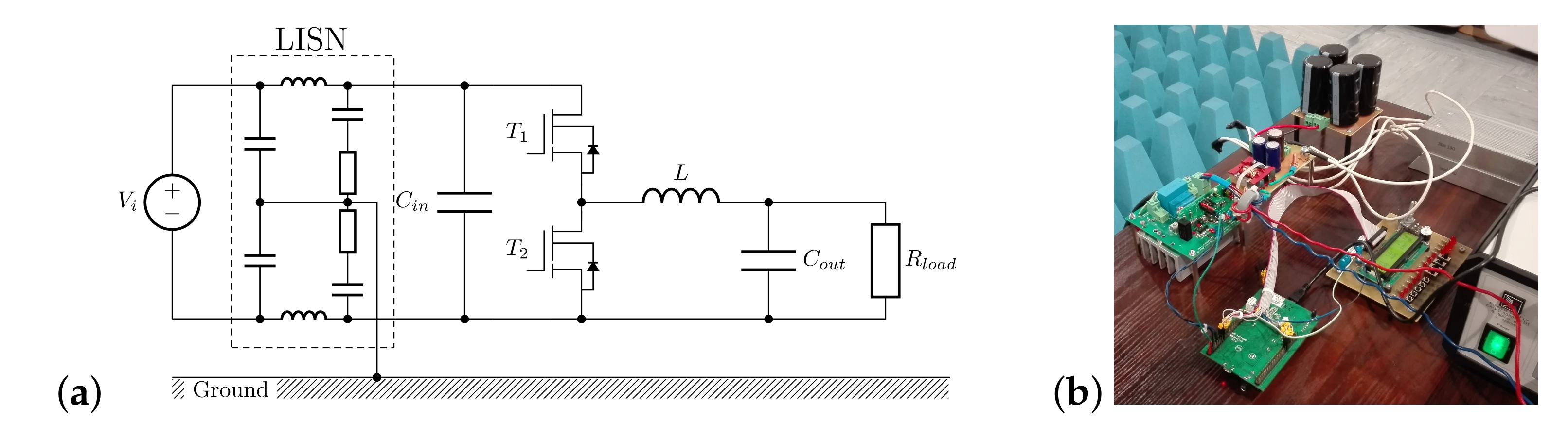
The converter including GaN HEMTs in cascode structure from Transphorm
(TPH3207WS: 650 V/50 A) supplied through the line stabilization network (LISN) Schaffner NNB 41 from the DC voltage source is presented in
Figure 1. The input capacitor
consisted of three parallel connected polypropylene capacitors (5
F, 10 nF, and 100 nF). The output low pass LC filter was sized to the cut-off frequency
= 1630 Hz. In the load
, the power of 350 W was dissipated at the output value
= 55 V. The gate driver based on Si8275 IC enabled control signal insulation and the output stage of the driver [
11]. This topology allows operating in synchronous and asynchronous mode. In this paper, the converter operation was tested in discontinuous current mode and triangular current mode [
12], where only the upper transistor was controlled and only the lower side reverse diode of the Cascode GaN structure was used.
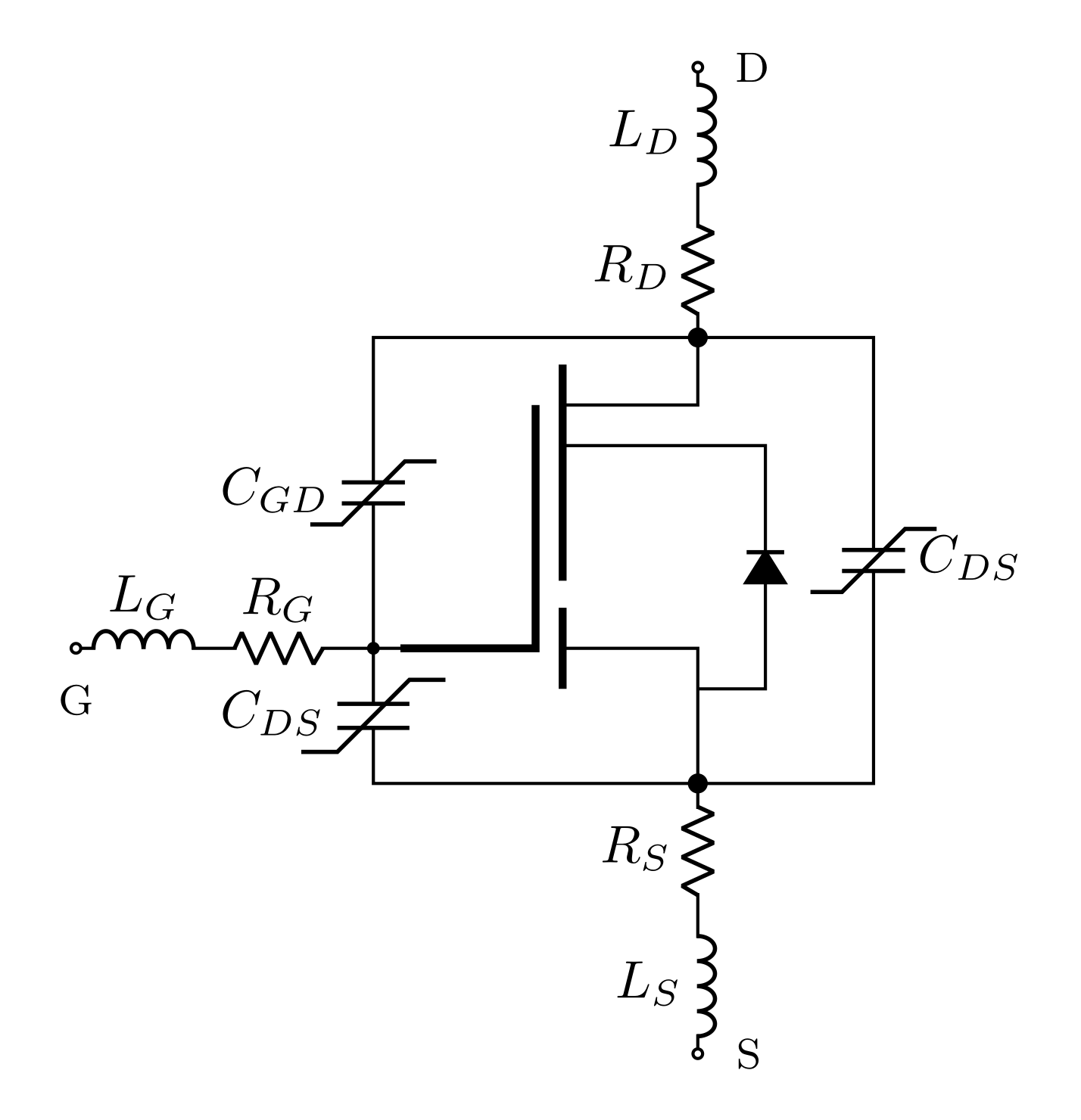
3. GaN HEMT Transistor Model
The GaN transistors are characterized by the possibility of changing their state in a very short time with the fast switching edges. The rapid changes in voltages and currents in the converter are the main origin of the EMI generation. The transistor model should reflect its dynamic including recharging of nonlinear capacitance. Moreover, the parasitic components should be included, because they are usually a part of the internal resonant circuit in the converter and play a great role in oscillation and overvoltage generation. The instantaneous value of internal capacitance depends on voltage
. The characteristics can be found in the manufacturer’s data sheet, but the given values there may be burdened with a statistical error that may significantly affect the simulation results. The wideband model of GaN transistor applied for simulation study is presented in
Figure 2.
The internal structure of the GaN FET transistor used is cascode of high-voltage GaN HEMT and low-voltage MOSFET [
13,
14]. Without knowing the internal structure, it is impossible to measure the capacitance of each of these transistors separately. Therefore, the capacitances have been modeled as it is presented in manufacturer data-sheet. Moreover, the tools included in Saber@Sketch allow to model only one internal transistor.
The parasitic capacitance of a transistor results from its internal structure, in which the areas with different potentials are very close to each other. Typical capacitance characteristics in transistor data sheets are input capacitance
, output capacitance
, and transfer capacitance
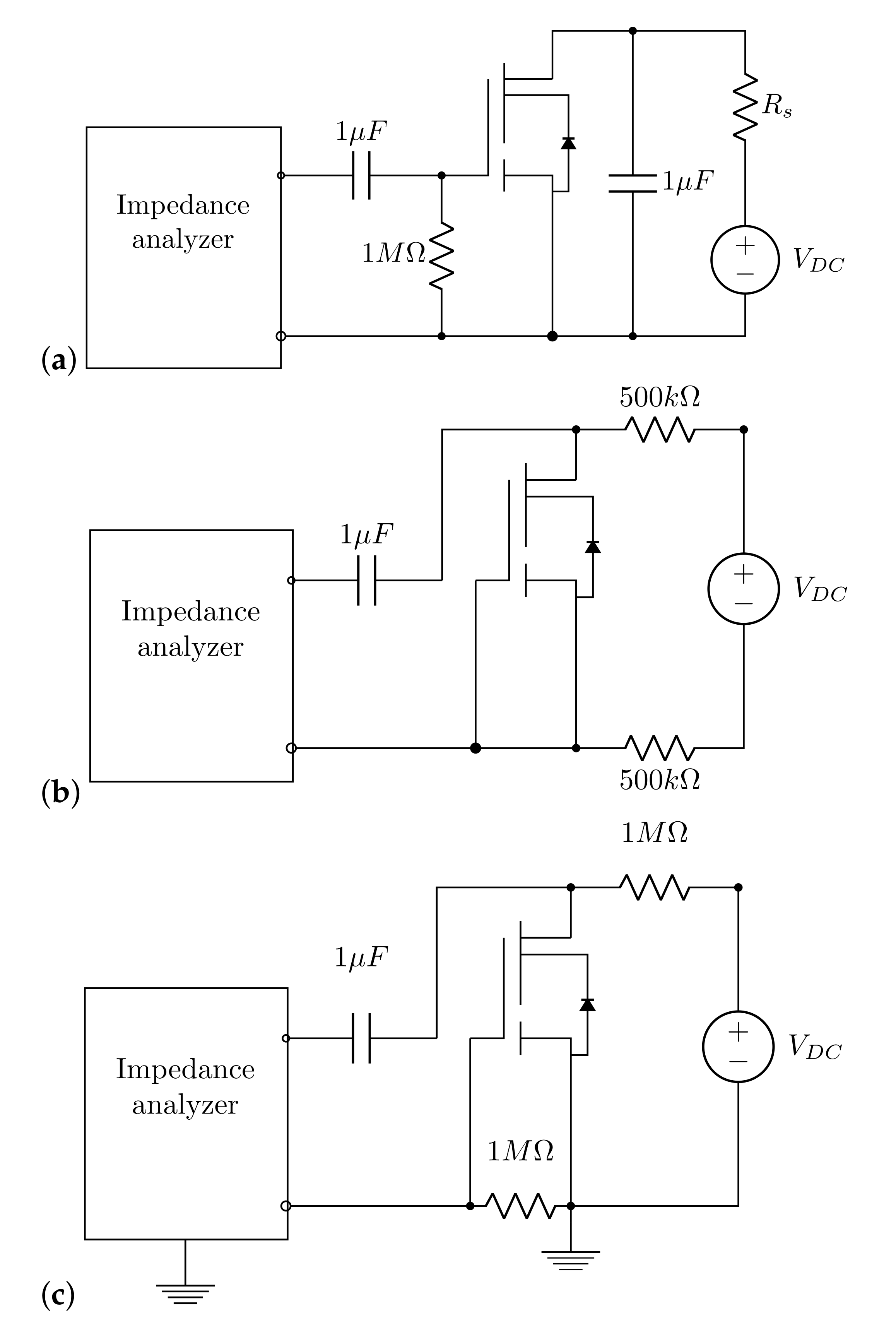
. In order to obtain a precise model, the characteristics of internal capacitances should be measured for the applied transistors. The direct measurement of these parameters with impedance analyzer or RLC bridge is not possible, because the mentioned devices do not provide a sufficiently high voltage, which should be applied between drain and source of the transistor. Accordingly, external auxiliary circuits have been proposed in [
15] enabling the measurement with suitable voltage range of
from an external source. The isolating ceramic or polypropylene capacitor
F connected to the impedance analyzer provides isolation between the measuring device and the positive node of DC voltage (
Figure 3).
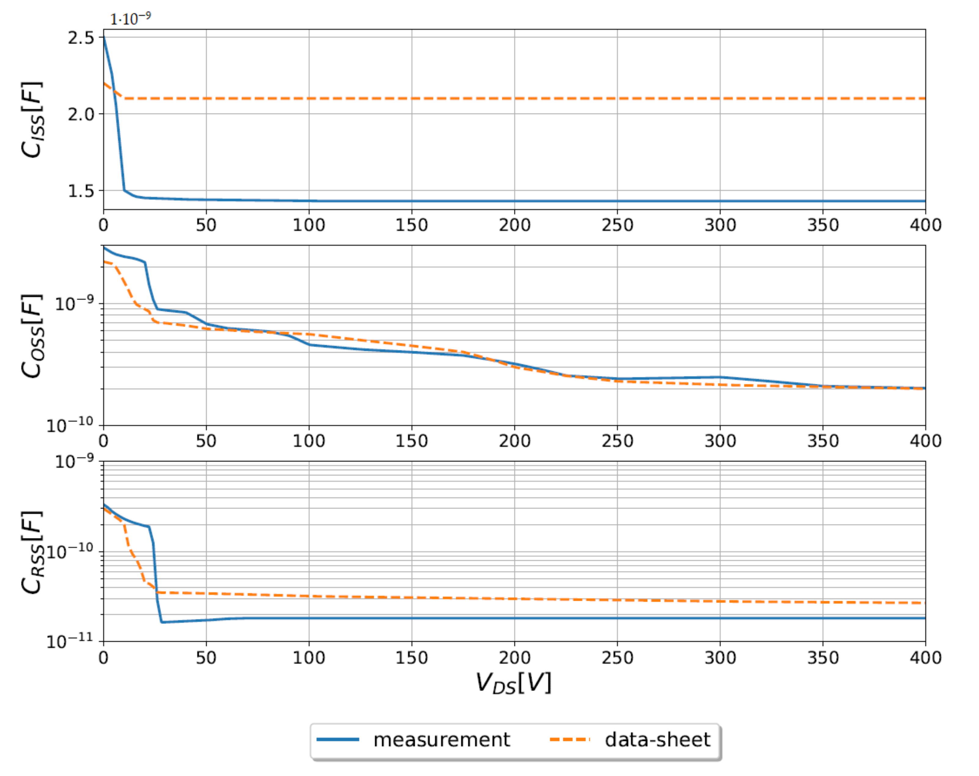
In the considered converter, the capacitances have been measured using impedance analyzer Keysight E4990A. The results of measurement are compared with data from producer data-sheet in
Figure 4. The presented differences— especially for
—result from the technological spread in the production of transistors. Note that in the simulation of experimental setup, such a discrepancy can cause significant errors.
The internal gate resistance is modeled as a series resistor and represents a combination of many internal resistances in a semiconductor structure. The value of this resistance is an important parameter as it directly influences the RC time constant of the gate and determines the maximum switching speed of the transistor. However, usually this parameter is not listed in data-sheets, but it can be measured. The gate resistance of the TPH3207WS transistor measured with an impedance analyzer is .
The total stray inductances of the transistors are composed of two different parts: internal and external (connections). The internal stray inductances cannot be measured by the user as there is no access to the internal structure of the transistor. Accordingly, the building of the transistor model should consider internal stray inductance (values delivered by the manufacturer in the datasheet or extracted from the simulation model) and external ones (measured by the user). The assembly technology affects the model to be accompanied by a parasitic inductance of connections of transistor-external stray inductance. For SMD (surface mount), inductances that come from connections could be neglected, but for THT (through-hole-technologies assembly) connecting wires should be included in the total value of
,
, and
(
Figure 2). The resistance of the connection is negligibly small. For the considered transistor housing TO-247, the connection is 10mm long, which results in parasitic inductance of about 10 nH (total stray inductance values:
= 12 nH,
= 13 nH,
= 11 nH). Note that these values are given for the nominal length of connections but in the real converter, they can be smaller because of the quality of mounting (shorter connections between TO-247 and PCB).
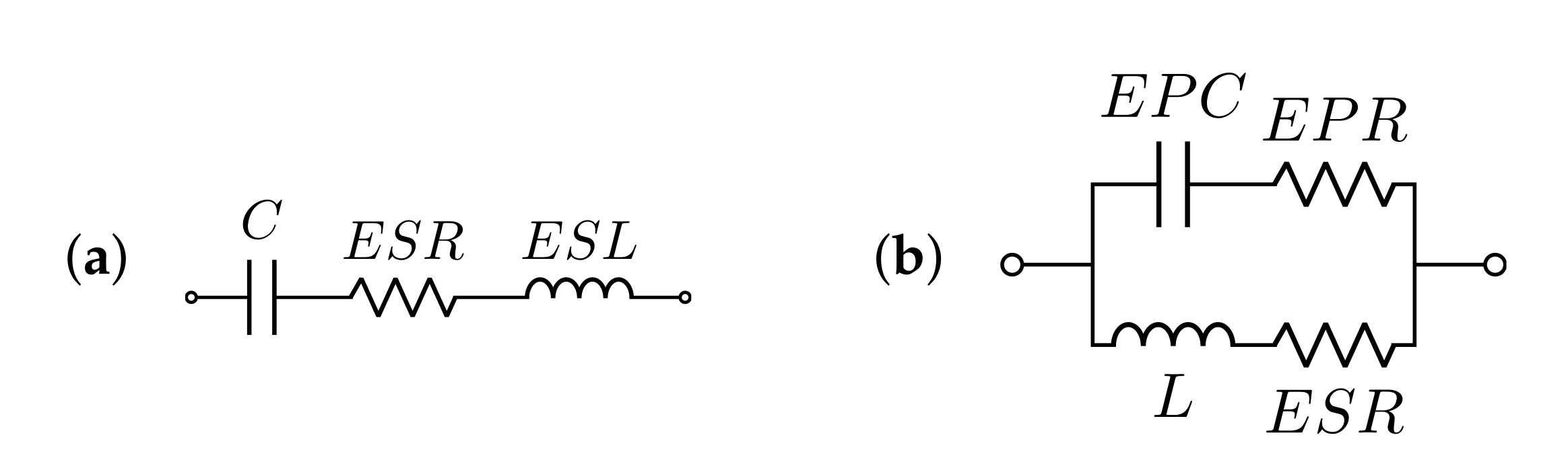
4. Passive Components Model
The widebanded passive component models—in addition to the basic parameter—should contain components that represent physical high-frequency phenomena such as ESR—equivalent series resistance, EPR—equivalent parallel resistance, ESL—equivalent series inductance, and EPC—equivalent parallel capacitance. The models of capacitor and inductor used in the simulation are presented in
Figure 5.
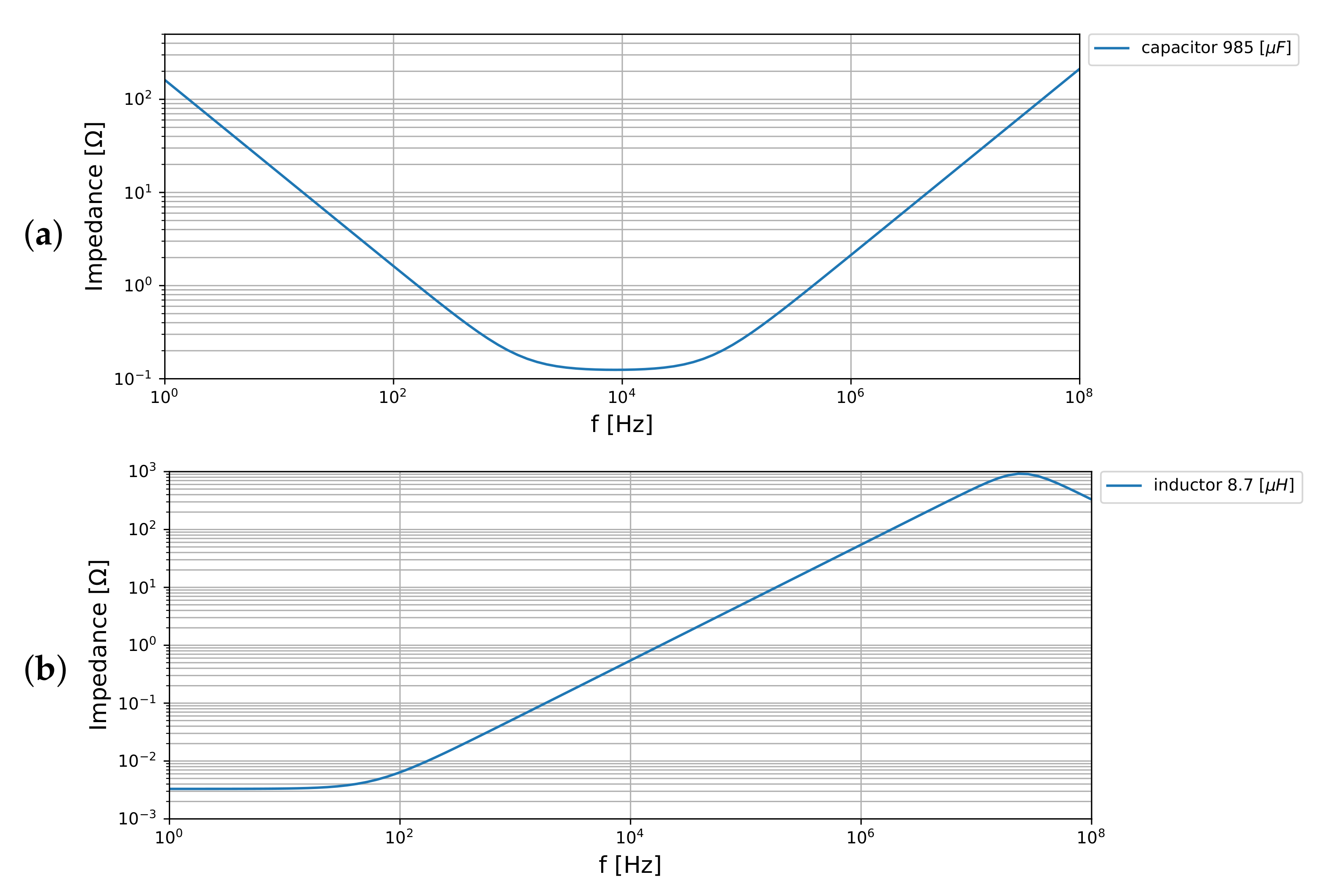
The parameters of input capacitor
and inductor L are presented in
Table 1 and their impedance in the frequency domain is presented in
Figure 6. Note that the character of impedance changes for higher frequency. The presented capacitor starts to behave like an inductor for a frequency above 10 kHz. Similarly, the impedance of the inductor changes its character in the frequency range above 26 MHz.
The equivalent circuit parameters of all passive components (as in
Figure 1a) have been measured using the impedance analyzer Keysight E4990A. The presented model of inductor gives proper results in conducted EMI frequency range, but it does not take into consideration the saturation of the core. If it is necessary to include saturation, the model should be extended [
16].
5. PCB Layout Model
The PCB layout, including the conducting tracks, wires, and cables, has primary importance in high-frequency behavior of the converter. The magnetic and electric couplings of conducting tracks can be represented by the coupled inductors and capacitors. These components are part of the resonant circuit responsible for overvoltages and oscillations at transistor turn off. Many software tools are offered to model PCB parasitics. In this paper, authors focus on the Q3D Extractor from Ansys and PEEC (Partial Element Equivalent Circuit) method [
17] used by InCa3d from Altair. The geometry of layout is defined or exported to the applied software environment and next ready-to-use model is generated. The PEEC method allows calculating the value of resistance and self- and mutual inductances using geometrical and physical properties of the tracks. The formulas can be directly implemented in the computing environment. In the presented example of buck converter, the PEEC method has been implemented in the Matlab software by authors. Based on formulas from in [
17], the Matlab functions have been written, where the input variables were entered manually in accordance to the dimension of the conduction tracks.
Using the Q3D Extractor, first sources and sinks should be defined and then the model including the following:
inductors equal to half of the inductance between two nodes,
inductive couplings between each inductor,
resistors representing AC and DC resistance of the tracks,
capacitors for capacitance between previously defined sources and between sources and artificial reference point.
Using the artificial reference points allows to define the capacitance between each conducting track and also the ground if it is placed within the circuit. However, the user has no access to this point in the generated ready-to-use model. Thus, the additional reference point of ground should also be included in the Q3D model. In the Q3D Extractor, models are generated for the one selected frequency, thus for other frequencies (e.g., harmonics) an inaccuracy may appear. However, the great advantage of these models is their numerical stability.
In the PEEC method, each conductor is segmented. Next, resistance, self-inductance and mutual inductance between each segment are calculated. In this approach, a frequency-independent model that takes into account skin or proximity phenomena is obtained.
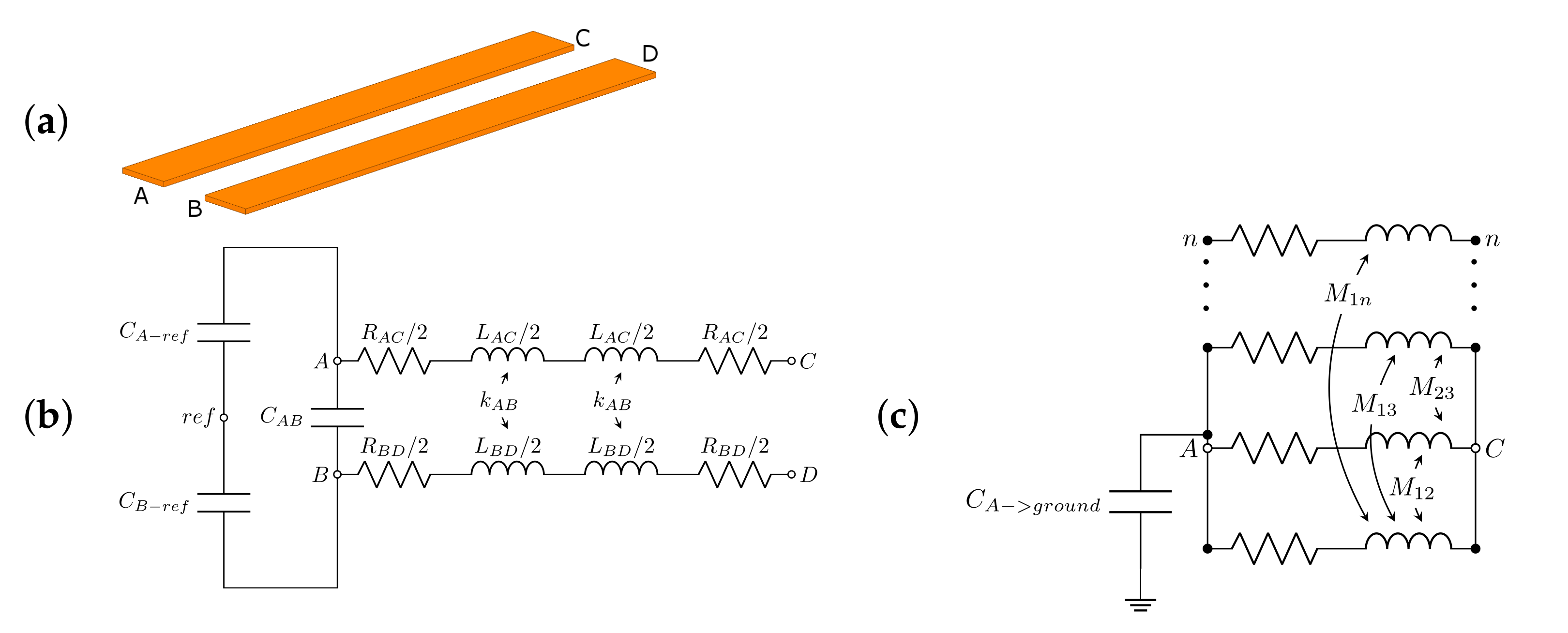
The topologies of both models are totally different. However, the simulation of both models should provide the same results. In order to show the differences, models of two conducting parallel tracks (two microstrip example) are shown in
Figure 7. The Q3D model of
Figure 7b includes RL components, capacitors between A and B sources, and a reference point. The C and D points were defined as sinks. The magnetic coupling is realized by the use of coefficient
k.
In order to keep the clarity of the diagram, the PEEC model of only one track is presented in
Figure 7c. It is divided into
n number of segments.
The presented circuit is simplified: the complete model should contain the same model of the second track and the mutual inductances M between all segments of both tracks and capacitance between them.
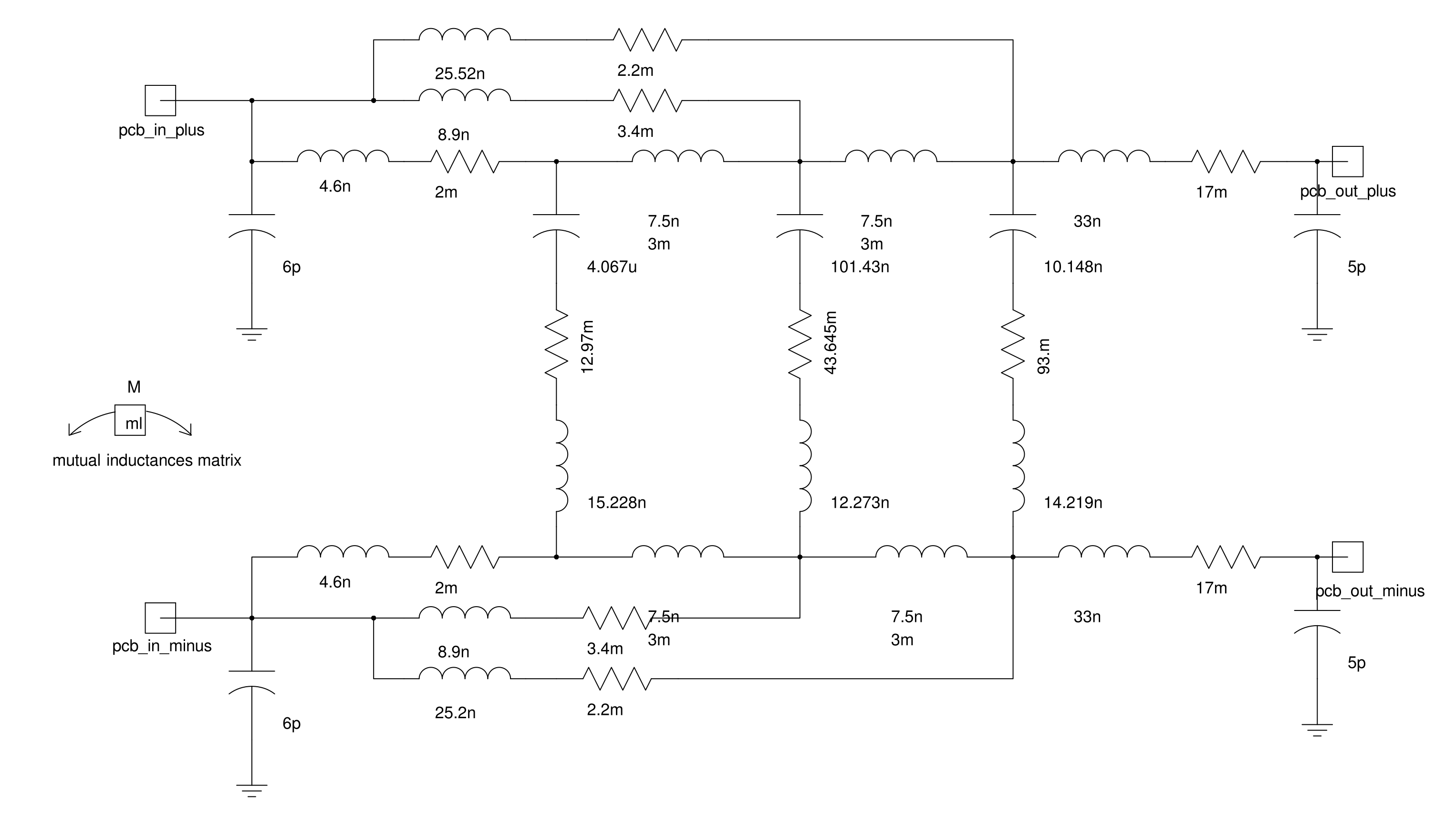
For the considered GaN HEMT buck converter, the parasitic inductances of PCB have been calculated using the PEEC method and parasitic capacitance to the ground with the Wheeler–Schneider formula [
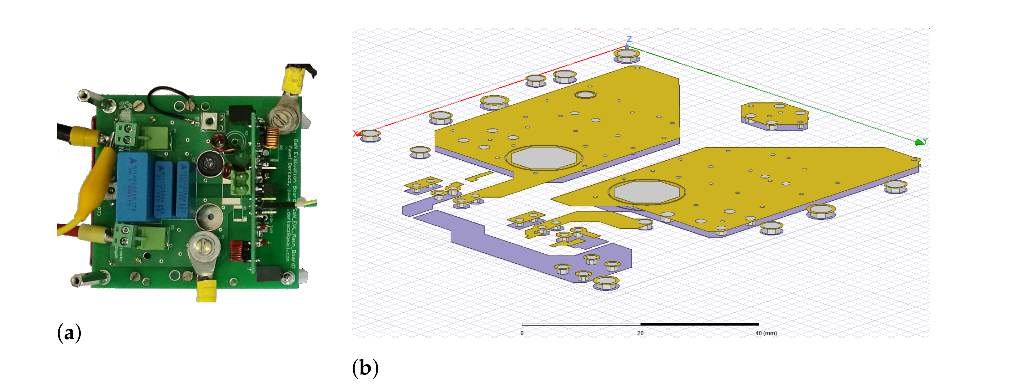
18]. The top view of the converter and the geometrical model is presented in
Figure 8. The Saber@sketch simulation schema of PCB and the three input capacitors from Saber@sketch is shown in
Figure 9. The conducting tracks are represented by lumped RLC components with the included matrix of mutual inductance M merged in MAST language. In order to show the range of values, the example parameters are shown in
Table 2.
6. Simulation Results
The wideband simulation circuit of buck converter from
Figure 1 was composed of the elements described in previous section of this paper using Saber@Sketch simulator from Synopsys Inc. The scheme includes the power supply
= 70 V, the inductance model of PCB layout as hierarchical circuit with lumped capacitors represented capacitance to the ground of main conducting tracks, semiconductors, and passive elements models. Moreover, the simplified model of transistor gate driver described in details in [
11] was included.
The entire simulation circuit can be a heavy burden on the simulation software because it contains numerous elements, including nonlinear elements. Therefore, it is necessary to check if that the calculations are free of calculation errors and that the whole system is numerically stable. The simplest and most effective method of checking the numerical stability is to run a series of simulations for various numerical conditions, e.g., calculation step or truncation error. If the simulation results do not differ significantly (there are any unexpected variations or an increase in the current and voltage values), it can be concluded that the obtained results are not burdened with numerical errors. If the results are not stable, it is recommended to add low value resistors in series with the nonlinear elements.
Another important aspect is adequate simulation time so that the circuit is in a quasi-steady state (all capacitors should be charged). In the Saber@sketch software, it is possible to continue the second simulation with initial conditions from the previous one. The simulation of the presented circuit was performed as follows:
the DC analysis was done in order to estimate all voltages quasi-steady state,
the time simulation with relative large calculation step (1 s) and long time (10 ms) to obtain the steady state (operation point) of the converter,
short time simulation (100 s) with a small step (1 ns).
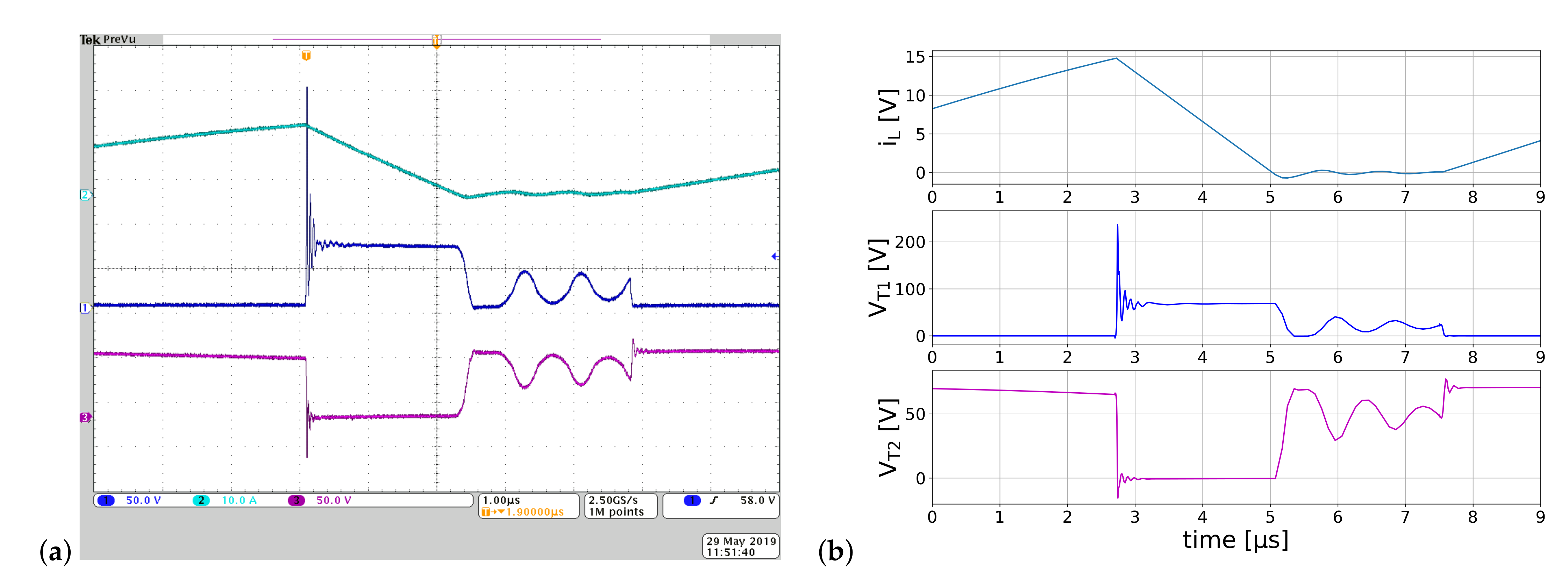
The results obtained with short time simulation are present in
Figure 10b and compared with the measurement. The inductor current
and voltages across both transistors waveforms are satisfactorily coherent in the time domain.
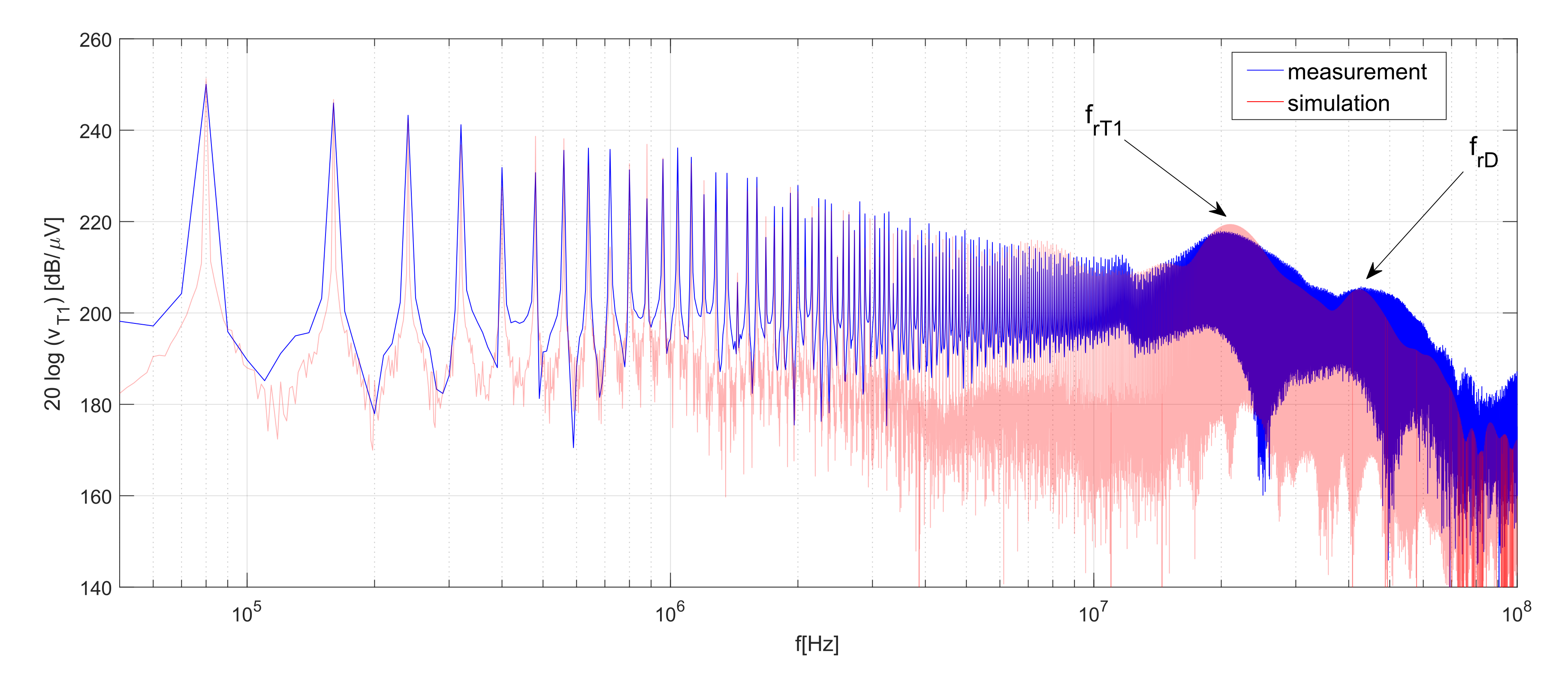
However, slight differences can be noticed when comparing the spectra. In
Figure 11, the spectra of voltages across the transistor
are compared. The levels of harmonics derived from the switching frequency are almost equal (up to 5 MHz). The peaks linked with ringing during transistor turn off (
∼ 21 MHz) and diode turn off (
44 MHz) overlap for simulation and measurement. The ringing frequencies depend mainly on the internal capacitance of semiconductor devices and the parasitic inductance of the input part of PCB.
Model Reduction
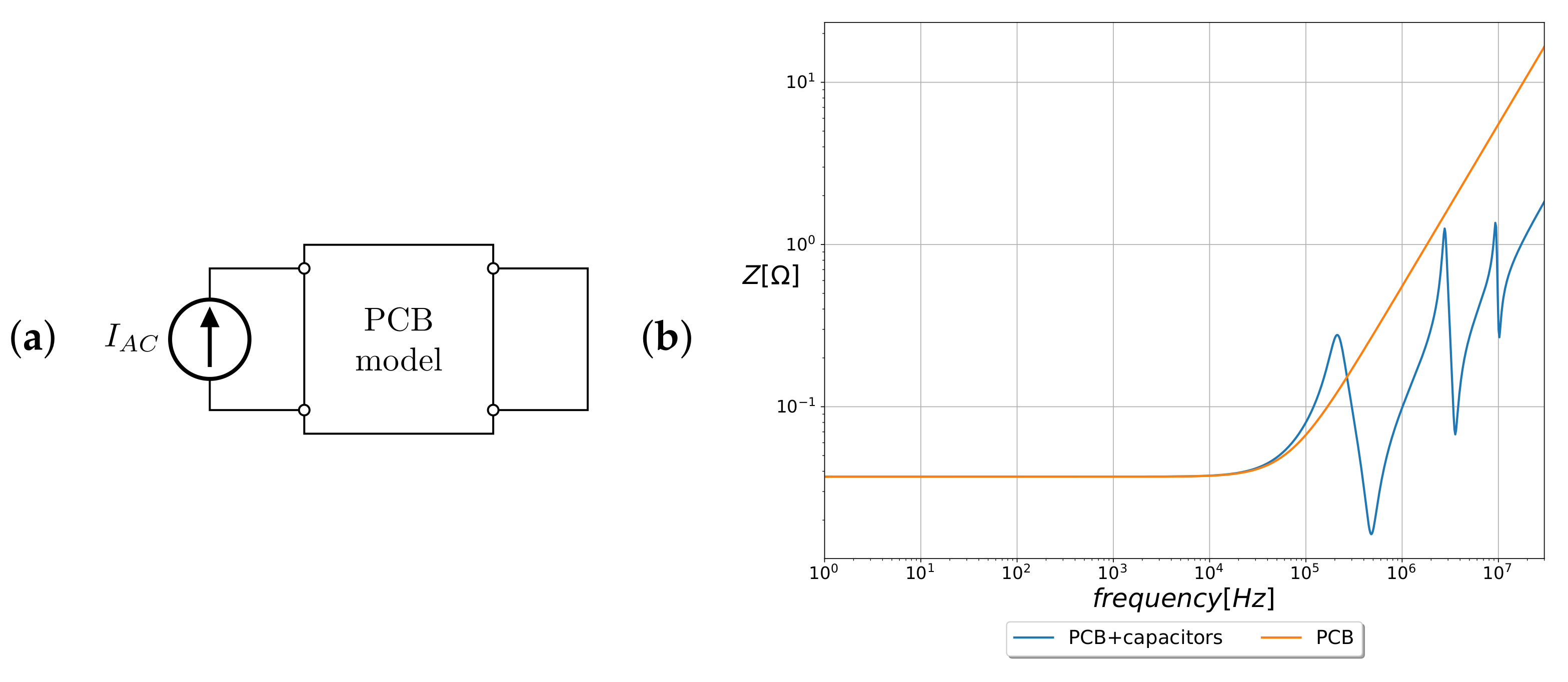
Usually, models obtained with calculation software can not be used in analytical analyses, so the reduction to a few lumped components model is applied. In [
10], the value of the leakage inductance was needed in order to calculate the value of overvoltage after commutation. The AC signal analysis has been performed to find the values of the lumped parasitic inductance of this part of the circuit. First, the model of tracks PCB of input filter was extracted and exported into circuit simulator Saber@Sketch (
Figure 9) and fed by AC current source equal 1A (placed on the high-side transistor location) as it is shown in
Figure 12a. The output of the PCB model was shortened. Using the results of the simulation, the impedance viewed from the current source was determined in the frequency domain. The calculations were performed in two cases: the first one with PCB tracks only, the second one with PCB tracks and three input capacitors included. Assuming that resistance is the dominant parameter for low frequencies, it can be read directly from the characteristic in
Figure 12b. For higher frequencies, the impedance equals the geometric sum of resistance and inductance, thus the value of inductance can be calculated using the Formula (
1).
For the considered buck converter, the calculation has been preformed for: Z(f = 1.4 MHz) =1 , R = Z(f = 1 Hz) = 30 m, which results = 113.63 nH.
Another method is to use the value of the first resonant frequency for the circuit including the parasitic inductance of PCB and three input capacitors using Formula (
2). The values for calculation are
= 208 kHz and
= 5.11
F, which result
=114.6 nH. The values from both methods should agree, but in this case the difference is 1nH, which may be due to non-precise frequency measurement.
7. Sizing of the Snubber Capacitor
The accurate wide-band modeling allows obtaining precise information about the overvoltage and ringing after semiconductor devices commutation. One of the examples (proposed by authors) can be solving the problem of unwanted overshoot. Presented simulation scheme was used to to design the attenuating component like the snubber. Usually, design procedure of the snubber is based on a laboratory measurement on the prototype after its realization. However, the simulation allows to do it on an earlier design stage and find optimal properties of components and adapt the layout to the required snubber.
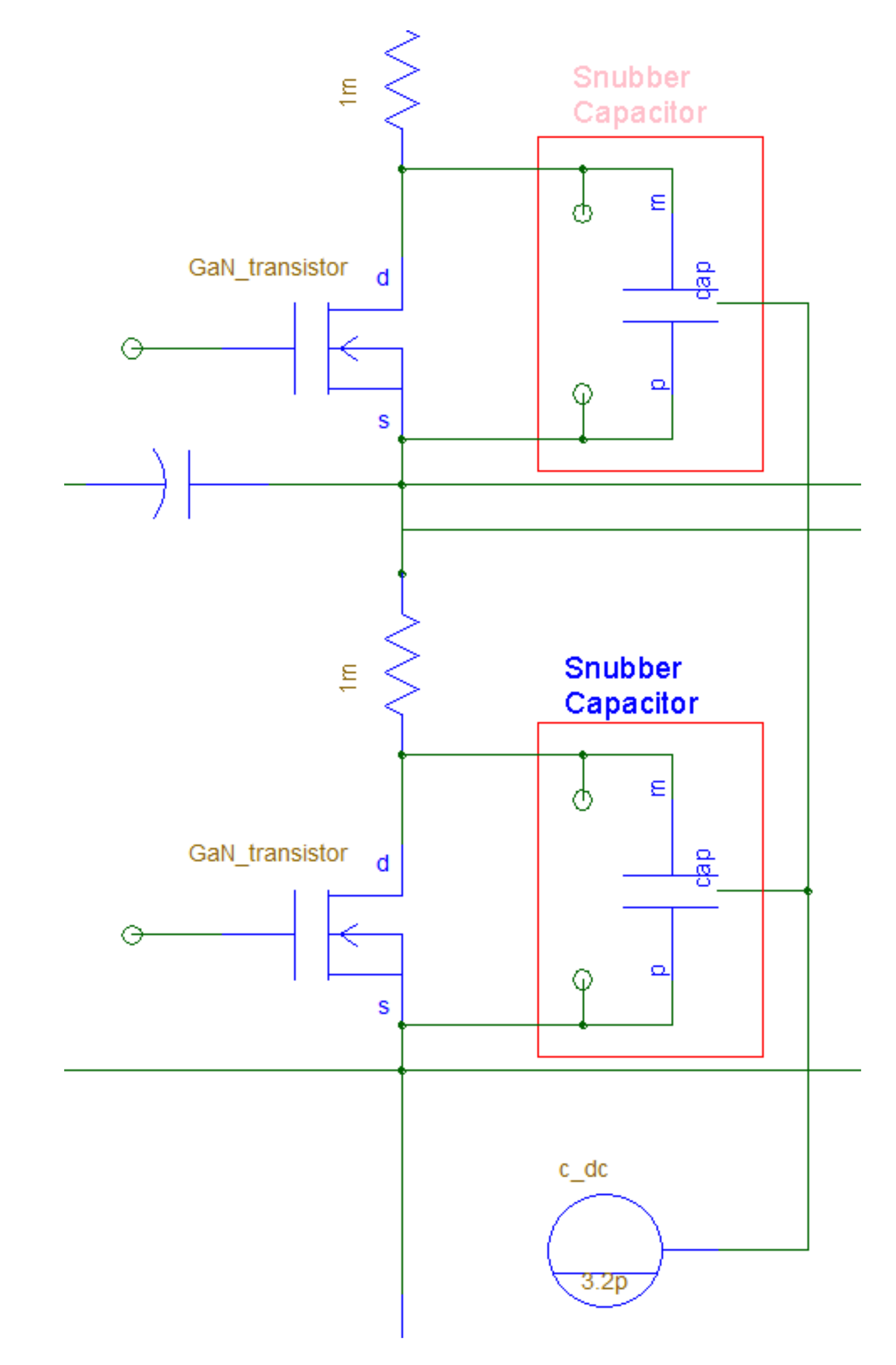
Using the varied parametric analysis in Saber@Sketch, it is possible to perform series of simulations for changing the value of one chosen parameter in the whole simulation circuit. The range and the changing step can be set in the software as “by step”, linear, or logarithmic. In order to find the optimal value of the snubber capacitor parallel connected to transistors, the model from Saber@Sketch library was modified. The value of capacitance was set using an external control signal source for both capacitors as it is shown in
Figure 13. Using the control source value as a parameter allows performing parametric analysis with changed capacitance value in both capacitors simultaneously. The simulation series were performed varying the snubber capacitors in the range from 10 pF to 10 nF.
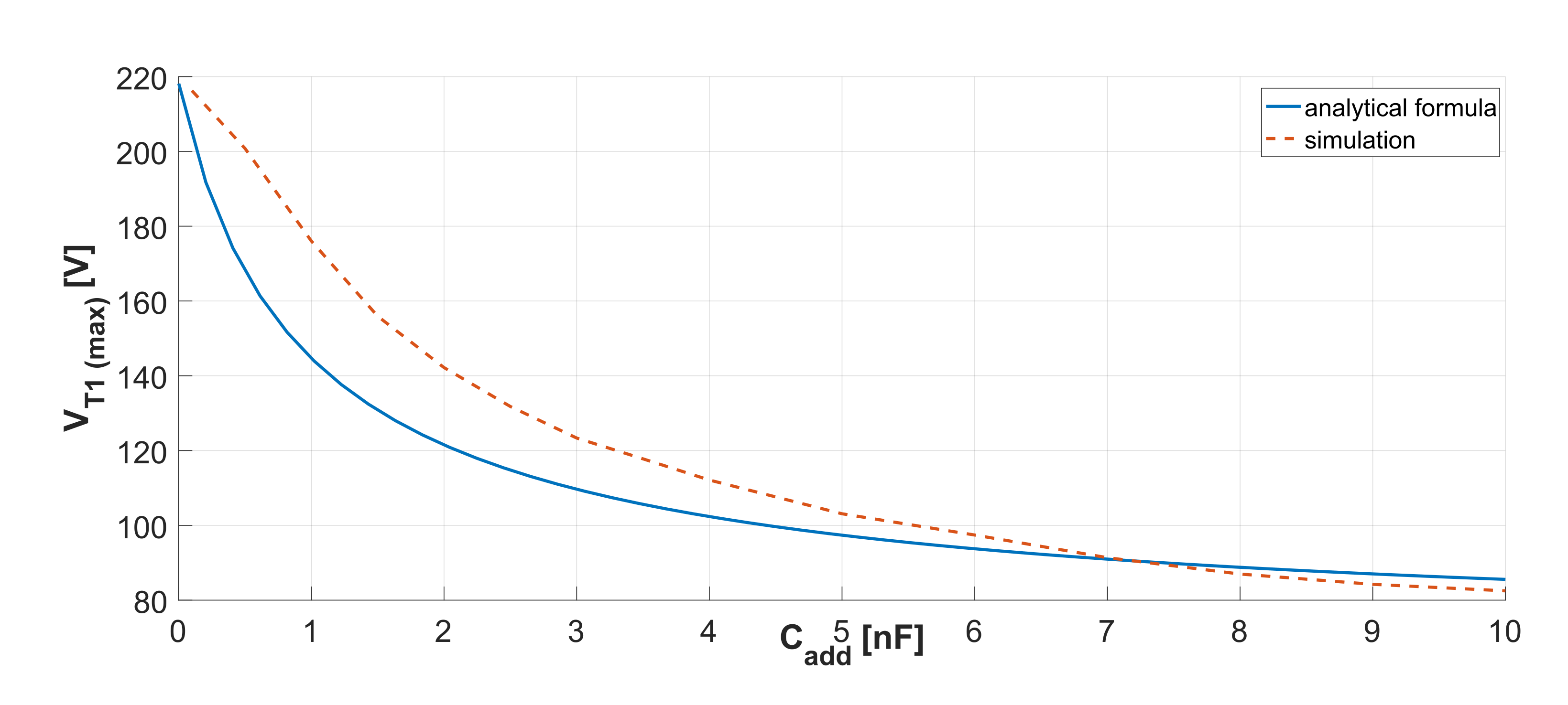
After extracting data from the result of the simulation series, the maximum value of voltage across the transistor
can be presented in the function of the snubber capacitance as in
Figure 14. The results are similar as presented in [
10], where the analytical formula was used.
8. Conclusions
The accurate forecasting of EMI generation and propagation allows ensuring the required levels of interference in the early design stage. The use of fast semiconductor switches, such as wide gap transistors, requires increased modeling accuracy and verification of parameters provided by the manufacturer. Models of all—both basic and parasitic—components should reflect their behavior in the entire required frequency range. In this paper, the modeling methodology is described and used on the example of DC-DC buck converter. The comparison of the obtained simulation results with waveform and spectra from measurement confirms the correctness of the method. Moreover, the model is used to extract the chosen parasitic parameter of the PCB and determine the optimal snubber capacitance value.
Author Contributions
Conceptualization, P.M. and P.B.D.; methodology, P.M. ; software, P.M. and P.B.D.; validation, P.M.; formal analysis, P.M. and P.B.D. and P.J.C.; investigation, P.B.D.; resources, P.J.C.; data curation, P.J.C.; writing—original draft preparation, P.M.; writing—review and editing, P.J.C. and P.B.D.; visualization, P.M.; supervision, P.M.; project administration, P.J.C.; funding acquisition, P.J.C. All authors have read and agreed to the published version of the manuscript.
Funding
This research received no external funding.
Conflicts of Interest
The authors declare no conflict of interest.
References
- Chen, Q.; Ye, F.; Chen, W. The prediction of conducted EMI on switched mode power supply based on full-circuit simulation. In Proceedings of the IEEE 2nd International Future Energy Electronics Conference (IFEEC), Taipei, Taiwan, 1–4 October 2015; pp. 1–5. [Google Scholar]
- Trinchero, R.; Stievano, I.S.; Canavero, F.G. EMI Prediction of Switching Converters. IEEE Trans. Electromagn. Compat. 2015, 57, 1270–1273. [Google Scholar] [CrossRef] [Green Version]
- Makarenko, Y.; Onikienko, Y.; Pilinsky, V.; Dovzhenko, O. Conductive EMI Modeling of Half-Bridge GaN Power Stage. In Proceedings of the IEEE 38th International Conference on Electronics and Nanotechnology (ELNANO), Kyiv, Ukraine, 24–26 April 2018; pp. 567–571. [Google Scholar]
- Mitani, K.; Kawamura, Y.; Kitagawa, W.; Takeshita, T. Circuit Modeling for Common Mode Noise on AC/DC Converter Using SiC Device. In Proceedings of the 21st European Conference on Power Electronics and Applications (EPE ’19 ECCE Europe), Genova, Italy, 2–5 September 2019; pp. P.1–P.10. [Google Scholar]
- Arribas, A.P.; Shang, F.; Krishnamurthy, M.; Shenai, K. Simple and Accurate Circuit Simulation Model for SiC Power MOSFETs. IEEE Trans. Electron Devices 2015, 62, 449–457. [Google Scholar] [CrossRef]
- Tian, M.; Hao, Y.; Wang, K.; Xuan, Y.; Huang, L.; Sun, J.; Yang, X. EMI modeling and experiment of a GaN based LLC half-bridge converter. In Proceedings of the 9th International Conference on Power Electronics and ECCE Asia (ICPE-ECCE Asia), Seoul, Korea, 1–5 June 2015; pp. 1961–1966. [Google Scholar]
- Mizoguchi, T.; Naka, T.; Tanimoto, Y.; Okada, Y.; Saito, W.; Miura-Mattausch, M.; Mattausch, H.J. Analysis of GaN-HEMTs switching characteristics for power applications with compact model including parasitic contributions. In Proceedings of the 28th International Symposium on Power Semiconductor Devices and ICs (ISPSD), Prague, Czech Republic, 12–16 June 2016; pp. 267–270. [Google Scholar]
- Okuda, T.; Nakamura, Y.; Hikihara, T.; Shintani, M.; Sato, T. Analysis of transient behavior of SiC power MOSFETs based on surface potential model and its application to boost converter. In Proceedings of the IEEE 4th Workshop on Wide Bandgap Power Devices and Applications (WiPDA), Fayetteville, NC, USA, 7–9 October 2016; pp. 101–104. [Google Scholar]
- Loncarski, J.; Monopoli, V.G.; Leuzzi, R.; Ristic, L.; Cupertino, F. Analytical and Simulation Fair Comparison of Three Level Si IGBT Based NPC Topologies and Two Level SiC MOSFET Based Topology for High Speed Drives. Energies 2019, 12, 4571. [Google Scholar] [CrossRef] [Green Version]
- Derkacz, P.B.; Musznicki, P.; Chrzan, P.J. EMI attenuation in a DC-DC buck converter using GaN HEMT. IEEE J. Emerg. Sel. Top. Power Electron. 2020. [Google Scholar] [CrossRef]
- Derkacz, P.; Musznicki, P. Gate Driver with Overcurrent Protection Circuit for GaN Transistors. PrzegląD Elektrotechniczny 2019, 2, 125–128. [Google Scholar] [CrossRef] [Green Version]
- Biela, J.; Hassler, D.; Miniböck, J.; Kolar, J.W. Optimal design of a 5kW/dm3/ 98.3% efficient TCM resonant transition single-phase PFC rectifier. In Proceedings of the International Power Electronics Conference—ECCE ASIA, Sapporo, Japan, 21–24 June 2010; pp. 1709–1716. [Google Scholar] [CrossRef]
- Lyu, G.; Wang, Y.; Wei, J.; Zheng, Z.; Chen, K.J. Dv/Dt-Control of 1200-V Normally-off SiC-JFET/GaN-HEMT Cascode Device. IEEE Trans. Power Electron. 2020, 36, 3312–3322. [Google Scholar] [CrossRef]
- Huang, X.; Li, Q.; Liu, Z.; Lee, F.C. Analytical loss model of high voltage GaN HEMT in cascode configuration. IEEE Trans. Power Electron. 2013, 29, 2208–2219. [Google Scholar] [CrossRef]
- Chen, Z.; Boroyevich, D.; Burgos, R.; Wang, F. Characterization and modeling of 1.2 kv, 20 A SiC MOSFETs. In Proceedings of the IEEE Energy Conversion Congress and Exposition, San Jose, CA, USA, 20–24 September 2009; pp. 1480–1487. [Google Scholar]
- Oliveri, A.; Lodi, M.; Storace, M. Accurate Modeling of Inductors Working in Nonlinear Region in Switch-Mode Power Supplies with Different Load Currents. In Proceedings of the 2018 15th International Conference on Synthesis, Modeling, Analysis and Simulation Methods and Applications to Circuit Design (SMACD), Prague, Czech Republic, 2–5 August 2018; pp. 233–236. [Google Scholar] [CrossRef]
- Ruehli, A.E. Inductance calculations in a complex integrated circuit environment. IBM J. Res. Dev. 1972, 16, 470–481. [Google Scholar] [CrossRef]
- Bogatin, E. Design rules for microstrip capacitance. IEEE Trans. Components Hybrids Manuf. Technol. 1988, 11, 253–259. [Google Scholar] [CrossRef]
| Publisher’s Note: MDPI stays neutral with regard to jurisdictional claims in published maps and institutional affiliations. |
© 2021 by the authors. Licensee MDPI, Basel, Switzerland. This article is an open access article distributed under the terms and conditions of the Creative Commons Attribution (CC BY) license (https://creativecommons.org/licenses/by/4.0/).


