1. Introduction
To improve the power delivering capacity, and reliability of power electronic converters, many researchers have directed attention towards the parallel connection of these converter units. Indeed, the parallel connection of converters have received increased attention in the past few years, due to several reasons; increased reliability through reduced number of conversion stages, modularity, ease of maintenance through the operation of identical units, scalable designs, and reduced size of the overall system [
1]. More significantly, such systems enable the integration of renewable energy sources and storage with the bulk electric grid [
2]. Analytical, and experimental verification of a scenario, in which multiple generators are connected in parallel, and how an interleaving scheme reduced the harmonics at the common point of connection, is discussed in [
3]. It explains how the parallel connection of multiple lower power units is used as a solution to design high power converters with better flexibility and higher reliability. However, one drawback of this kind of parallel-connected system [
2,
3,
4] is that, due to the common AC point of connection, the integration of renewable resources becomes difficult. Additionally, in the multi-converter systems explained in [
1,
5,
6,
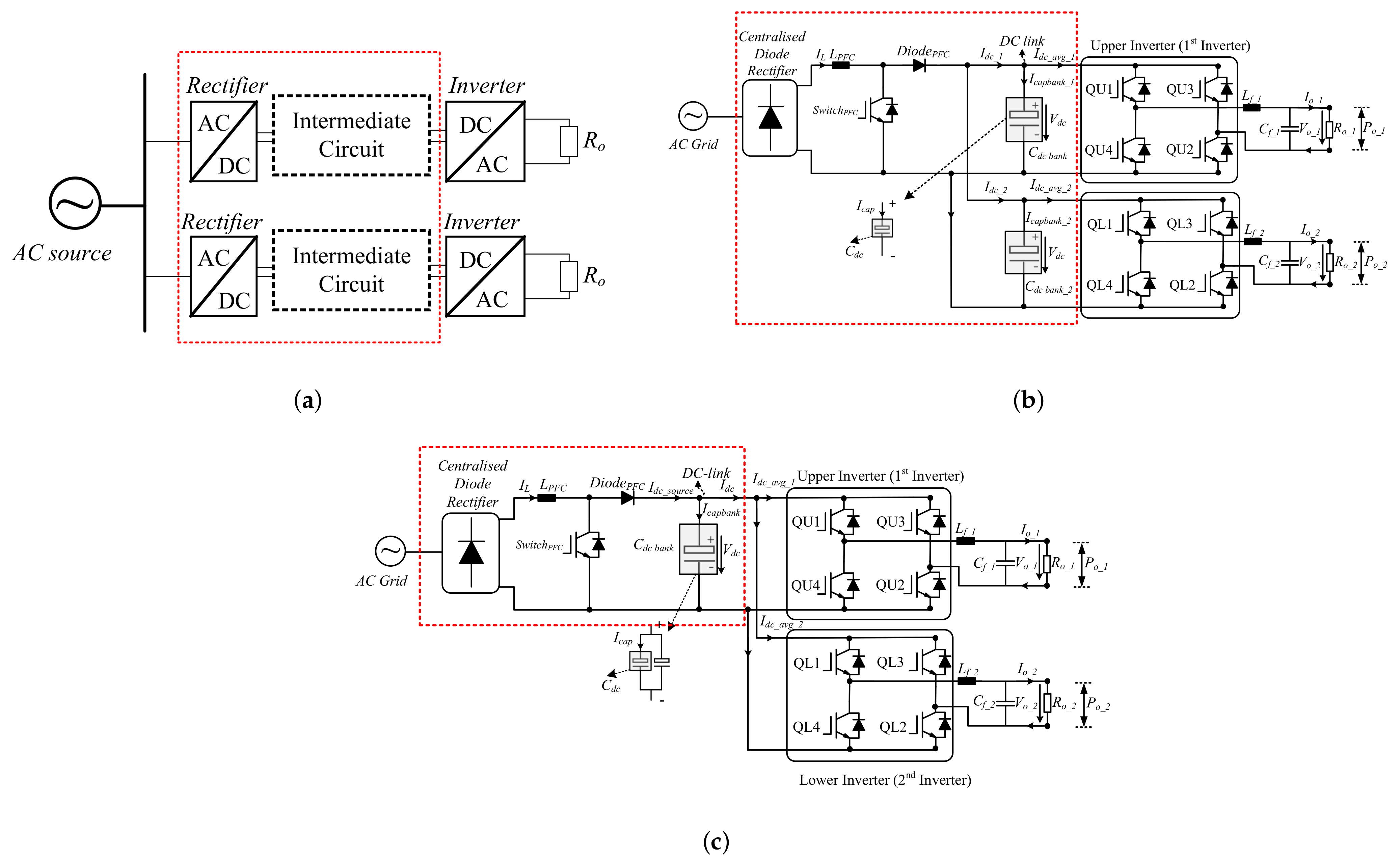
7], each inverter has its own individual rectifier system and shares the common DC-link, an example of which is shown in
Figure 1a. Hence the total number of rectifiers needed in the whole system increases, eventually increasing the overall size and reducing reliability.
Even though in industrial applications, DC-connected parallel inverter systems are gaining popularity, such parallel systems generate excess current ripple (harmonics) at the DC-link due to the harmonic interactions between the inverters, in addition to the harmonics from the pulse width modulation switching. This harmonic interaction at the DC-link causes the failure of fragile components such as DC-link capacitors [
1,
4]. This is of significant importance as the current ripple causes a decrease in the capacitor lifetime due to an increase in the internal temperature. The power loss of the capacitor, which is a function of the current harmonic spectrum and its Equivalent Series Resistance (ESR), also increases as the capacitor current increases [
8]. Several studies show that 30% of the total failure root causes in the power electronic systems are due to capacitor failures [
9], and hence, they are considered the most fragile components in a power electronic system [
9,
10,
11,
12]. In order to extend the lifetime of the DC-link capacitor, two possible solutions are considered. One practical solution in the market is to use higher capacitance and a higher rated current capacitor at the DC-link, but the total volume, weight and cost will significantly increase. Another way is to actively reduce the current stresses of the DC-link capacitor. This method is considered in this paper for a parallel-connected inverter system, which is more cost efficient and convenient to use due to no hardware change being needed. Because in a parallel system the DC-link current is generated by a summation of the current harmonics from the connected converter, the phase-shifted switching cycles lead to variations of the current ripple [
5]. Thus, using an interleaving (i.e., phase-shifting) of the PWM carrier waves of the inverters at an optimal angle is a possible solution to effectively reduce the total DC-current ripple at the DC-link.
A plethora of research has been conducted on interleaving the carrier waves of the parallel-connected PWM inverters to reduce the DC-link current harmonics [
1,
2,
3,
4,
5,
7,
13]. Lowering the DC-link harmonics reduces the power losses within the capacitor [
14]. In a parallel-connected system, the phase-shifted switching cycles of the carrier waves can effectively reduce the current ripple; as a result [
7], the size and weight of passive components, such as the DC-link capacitors and EMI-filters, can be reduced. A detailed study of a harmonic reduction technique using synchronized phase-shifted PWM voltage source inverter (VSI) units having an individual DC-source has been provided in [
1]. Alternatively, ref. [
5] presents the effect of an optimal phase-shift angle on reducing DC-current ripples under unequal DC-link voltage scenarios in two parallel three-phase grid-connected voltage-source inverters (VSIs). The effect of the size of the DC-link components and the grid configuration in three-phase multi-drive systems, similar to the topology shown in
Figure 1a, on the resonant frequencies, have been studied in [
6]. In [
7], analytical modeling of paralleled and interleaved 3-level neutral point clamped inverters using space vector modulation is discussed. It explains how interleaving helps to reduce both AC and DC-side harmonics and reduces the EMI harmonics in parallel-connected inverter systems. To minimise the DC-capacitor size, a coordinated PCC voltage harmonics mitigation strategy is discussed in [
15] for parallel inverters by properly shaping inverter output impedance. Similarly, a harmonic damping approach using a point of common-coupling (PCC) voltage control for multi-parallel inverters is discussed in [
16]. Even though these techniques seem to be promising solutions to mitigate DC-link harmonics, complexity has become the main obstacle for these harmonic elimination approaches in multidrive systems.
As mentioned above, the existing methods for multi-converter systems, to the best of the authors’ knowledge, have the following two limitations: Firstly, most of them consider common AC-grid connection for the parallel inverters, which limits the integration with the DC-grid system, and renewable energy resources. Secondly, there is no DC-link current harmonic elimination method proposed for multiple drive systems with a common DC-link in any of the pieces of literature so far. To address these research gaps, this work presents a carrier phase-shifting strategy for two different configurations of common DC-connected multi-converter systems. The two key contributions of this paper are:
A family of common DC-link structures is proposed, where one topology is a multi-converter system with an individual DC-bank (shown in
Figure 1b), and another topology is a multi-converter system with a common DC-bank (shown in
Figure 1c). In a traditional system, as seen in
Figure 1a, each inverter has its own individual rectifier system and shares the common AC link. Compared to this kind of system, the proposed systems in
Figure 1b,c have the following advantages. In the proposed multidrive system, the overall system cost would be less: in the traditional system each inverter has its own rectifier, and the cost for two rectifiers has to be considered, which will increase the overall cost. However, in the proposed systems, due to the implementation of a centralized rectifier, the cost would be less. Secondly, due to the reduced number of power electronic components (rectifiers) in the proposed system, the reliability will be higher. Moreover, a centralised rectifier provides the flexibility for plug-and-play of the number of inverters connected to the DC-grid in parallel-connected systems. Notably, this kind of operation allows for the easy integration of DC sources at the common DC link in a system, compared to the conventional parallel-connected system.
Besides that, this paper proposes a new modulation method to reduce the DC-link capacitor requirement via phase-shifting of the carrier waves, which is a value-added technology. It does not need to change any hardware in the system, while the DC-link ripple and capacitance can be reduced, which benefits the cost, volume and weight of the system. The optimally phase-shifted switching cycles lead to variations of the output current ripples, which, when summed together in the common DC, results in the minimization of ripples at the DC-link current. Thereby, the switching frequency harmonics reduce, which reduces the overall DC-capacitor RMS current; hence, reducing the overall stress (electro-thermal stress and hot-spot temperature) at the DC-link, leading to an improved lifetime of the DC-link capacitor.
This paper is structured as follows. The overall system description is presented in
Section 2.
Section 3 discusses the harmonic analysis of the capacitor current based on the conventional system, and
Section 4 explains the proposed system. The lifetime estimation is discussed in
Section 5. The effectiveness of the developed analysis is demonstrated by the results and discussions in
Section 6. Finally, conclusions are drawn in
Section 7.
2. Proposed System Description
In this study, a diode rectifier with a boost power factor corrector (PFC) and a DC-filter (consisting of a DC-choke and a large electrolytic DC-link capacitor) is implemented due to its simplicity, cost-effectiveness, and reliability advantages [
6]. Aluminium electrolytic capacitors (El-caps) are used as DC-link capacitors, due to their advantage of providing a high capacitance per unit volume at low costs compared to other types of capacitors [
17]. The boost PFC employed improves the power factor, as well as facilitates power supply hold-up, which ensures that the system can maintain the DC voltage until the backup power supply is connected, in case of a power supply disruption [
18,
19].
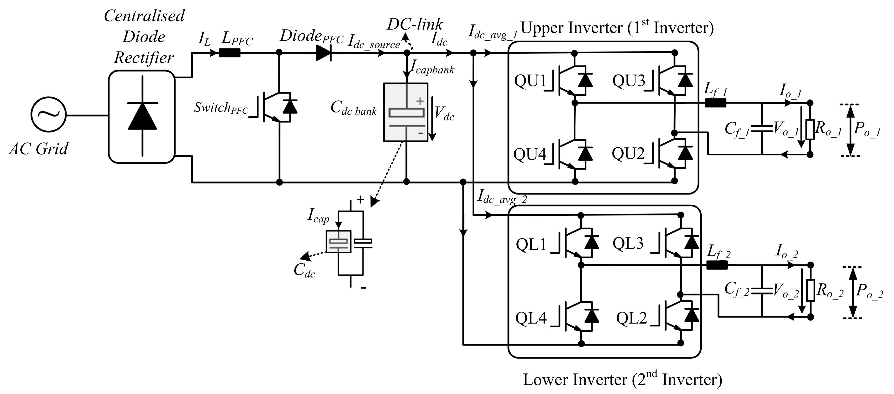
The proposed topologies in this paper, shown in
Figure 2 (hereby referred to as the multi-converter system with individual DC-bank) and
Figure 3 (hereby referred to as the multi-converter system with common DC-bank), have a centralized rectifier and a common DC point to connect the parallel inverters. The two inverters in the proposed system are in the same phase and have the same output waveforms, as they are to be used for a single application process, for example, in a sugar production plant, where multiple motors are operating at the same speed, frequency and power, or for applications such as the air conditioning and cooling systems in a dairy factory. More importantly, a DC-link current harmonics mitigation strategy is introduced via phase-shifting of the inverter carrier waves in these two topologies. Using a centralized rectifier eliminates the need for each inverter to have its rectifier, as shown in
Figure 1a. For the proposed multi-converter system with individual DC-banks, each of the parallel-connected inverters has its individual capacitor bank to limit the DC-link voltage fluctuation. This kind of connection provides more flexibility to the industrial designers to plug-and-play with the number of inverters connected to the DC-grid in parallel-connected systems. On the other hand, the proposed multi-converter system with a common DC-bank has a common capacitor bank consisting of individual capacitors, which are connected in parallel to ensure the equal distribution of the ripple current (
) flowing through the the DC-link capacitor bank (
). The total ripple current flowing through (
) is denoted by (
), and through a single capacitor by (
).
The four switches
,
,
,
of the VSI units, shown in both
Figure 2 and
Figure 3, are controlled using the unipolar sinusoidal PWM (SPWM) technique, explained in detail in [
20,
21]. The specifications of the inverter system and output filter (designed according to [
21]) are given in
Table 1 and
Table 2. Both the topologies (in
Figure 2 and
Figure 3) have the same parameters and loading conditions. The rated output voltage of 230 V (RMS value) for each inverter unit is maintained by its own specific Proportional–Resonant (PR) controller, which is designed according to [
22,
23]. The control algorithm for the inverter is shown in
Figure 4a, and for the boost, PFC is shown in
Figure 4b. The parameters for the controllers have the same value, as both VSI units are synchronized and controlled using unipolar SPWM to obtain the same
. The parameters for the boost PFC are shown in
Table 3, designed according to [
24,
25]. The data for the DC-link capacitor are from the data sheet in [
26] and are shown in
Table 4.
4. Proposed Method with an Optimal Carrier Phase-Shift
For the multi-converter systems shown in
Figure 2 and
Figure 3, one of the effective methods to reduce the DC-current ripple is interleaving the carrier signals of the parallel converters. Both the inverters connected to the common DC-link are considered to be in synchronisation with each other, and have the same operating conditions mentioned in
Table 1. To apply the proposed DC-link harmonic mitigation method, it is necessary to first find the optimal phase-shift angle (
) for the carrier signal, which provides maximum capacitor current ripple cancellation (i.e., at the main switching frequency harmonic component which appears at
= 40 kHz). The optimally phase-shifted switching cycles lead to variations of the output current ripples, which when summed together result in the minimization of ripples at the DC-link current. This is analytically explained in (
1)–(
9), provided below, for inverters that have unipolar PWM [
27]. In this paper, the phase shift is applied to the lower inverter carrier signal, therefore the phase angle of the upper inverter carrier signal is
, whereas the phase angle of lower inverter carrier signal is
=
.
In the above equations,
present upper and lower inverter output voltages and output currents. The peak value of the output currents of upper and lower inverters is
The DC-current source and the average value of its upper and lower inverters are represented by
The capacitor bank current for upper and lower inverters is denoted by
Finally, the fundamental frequency and switching frequency of the upper inverter are symbolised by
and that of the lower inverter is designated by
(
1)–(
4) describe the upper inverter, while (
5)–(
8) is for the lower inverter. (
3) and (
7) are derived based of the power balance equation of the inverter, which states that the input power on the DC-side
of the converter relates to the output apparent power on the AC-side
.
The method used in this paper is as follows: firstly, various phase-shift angles are applied for the carrier signal of the lower inverter (
), and the multi-converter system with individual DC-banks (shown in
Figure 2) is simulated using PLECS, under the rated operating conditions mentioned in
Table 1. Then, the harmonic spectrum (
Figure 6b) and the ripples in the time domain waveform (
Figure 7b) of the total capacitor current are studied to find the phase-shift angle at which maximum high-frequency harmonic ripple cancellation occurs, which produces the minimum of the overall RMS value of the DC-capacitor current. This will be the optimal
The same method is applied to the multi-converter system with a common DC-bank shown in
Figure 3 to obtain its optimal carrier phase-shift angle.
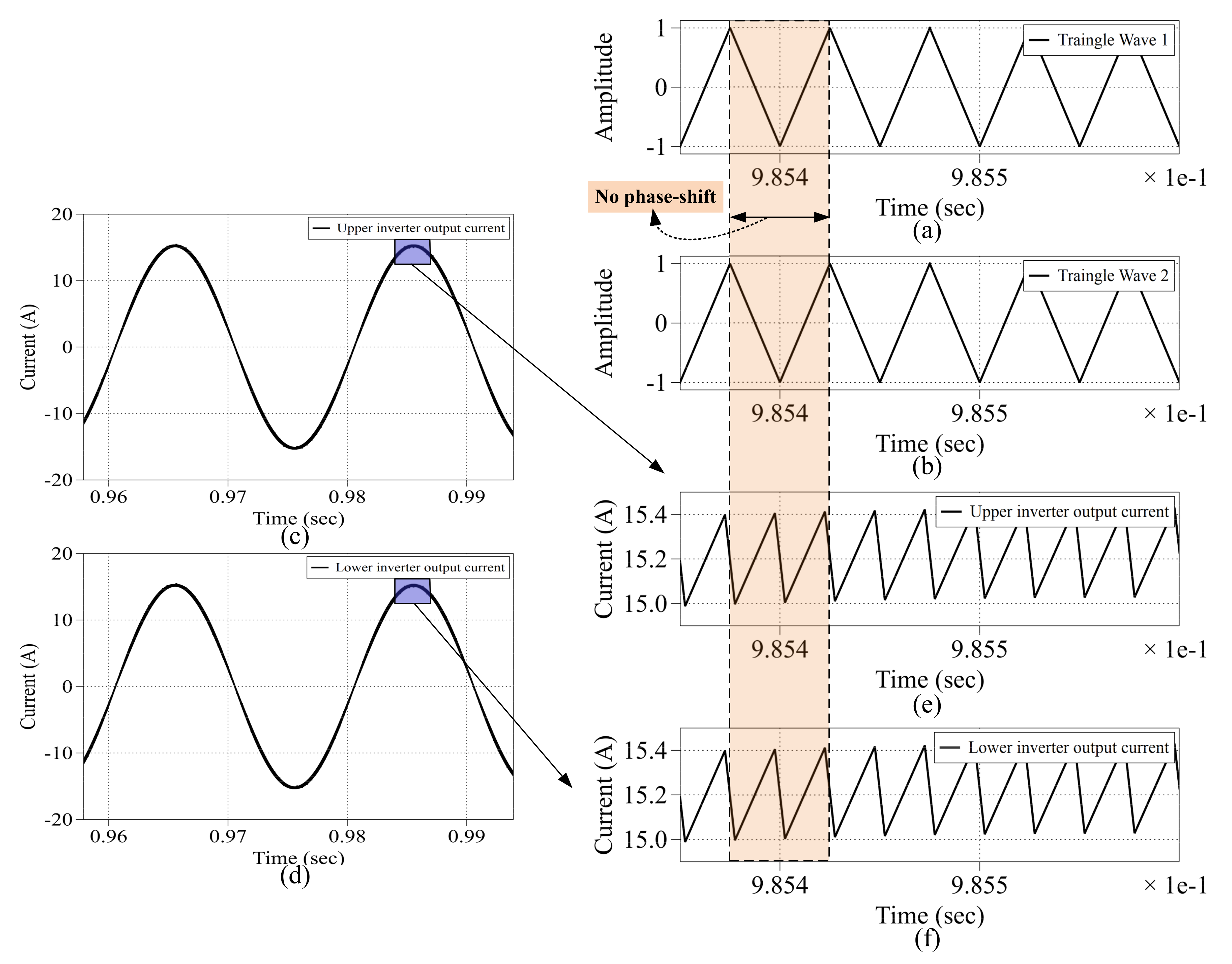
The switching frequency harmonic component
= 40 kHz is shown for various phase-shift angles (
) applied to the carrier frequency of the lower inverter for the multi-converter system with a common DC-bank in
Figure 6a and the multi-converter system with individual DC-banks in
Figure 6b. At
(violet colour bar), there is no phase-shift applied and this case scenario is taken for the system using the conventional method. Among the various phase-shift angles analyzed, it can be seen that the harmonic ripple (
= 40 kHz ) is at a minimum when
, denoted by the red color bar in
Figure 6a, and the green color in
Figure 6b. Thereby, it can be observed from
Figure 6 that both the topologies (shown in
Figure 2 and
Figure 3) have a minimum main switching frequency harmonic component (
= 40 kHz) and a maximum DC-capacitor current ripple cancellation at
Furthermore, at a
carrier phase-shift angle, there is maximum ripple cancellation in the DC-capacitor bank current as illustrated in
Figure 7. It can be understood that the capacitor current ripple is almost half the value (red dotted line) when compared to the scenario in which there is no phase-shift applied (violet line) in both the multi-converter system with individual DC-banks and with a common DC-bank. Accordingly, from
Figure 6 and
Figure 7, it can be concluded that the optimal phase angle is found to be when the two carrier signals for the two inverters are phase-shifted by
The optimally phase-shifted switching cycles lead to variations of the output current ripples, which when summed together result in the minimization of ripples at the DC-link current as shown in
Figure 8e. The reduction of the DC-capacitor current ripples means that the switching frequency harmonics reduce (since a unipolar SPWM is used, for
= 20 kHz, the main switching frequency harmonic component appears at
= 40 kHz). Consequently, the overall DC-capacitor RMS current decreases, thus reducing the overall stress (electro-thermal stress and hot-spot temperature) at the DC-link. Hence, the proposed scheme shown in
Figure 8 (in red line) helps to reduce harmonics, and thereby the total harmonic distortion (THD) in the DC-capacitor current. Without any phase-shift, the THD =5.8% for the capacitor current and, after applying the proposed optimal phase-shifting, the THD reduces to 2.7%, calculated as in [
28].
5. Lifetime Estimation of DC-Link Capacitor
Reducing the harmonics ripples in the DC-capacitor current helps to improve the lifetime
of the DC-capacitor as the overall electrical and thermal stress in the capacitor significantly decreases [
17]. The lifetime prediction model used in this paper is shown in
Section 5 and explained in detail (including the equivalent circuit model of capacitor) in [
28].
is the rated lifetime of the capacitor at rated voltage
, and rated upper category temperature
(given in
Table 4).
is the temperature factor and
is the voltage ripple factor. V is the actual operating voltage. The value of the exponent
p is between 3 and 5 for El-caps [
17]. The hot-spot temperature
of the DC-capacitor, estimated by (
11), depends upon the operating temperature and
on the power loss of the capacitor (which is a function of ripple current and ESR). Considering the heat dissipation from the diode bridge, DC-link filter, and inverter, the operating temperature
is defined as 40–60
C instead of room temperature [
14].
can be estimated by (
12).
where
is the RMS value of the harmonic ripple current at frequency
, obtained from the harmonic spectrum of the capacitor current.
is the ESR at the
frequency
.
is the thermal resistance of the capacitor between the hot spot and the ambient temperature. The rated values for the chosen capacitor (KEMET AlS8(1)(2)392NF500) in this paper are given in
Table 4.
6. Results and Discussion
In this section, the effectiveness of the proposed harmonic mitigation for both the multi-converter system with a common DC-bank and the multi-converter system with individual DC-banks is analyzed through experimental and simulation results.
As shown in
Figure 2 and
Figure 3, the multi-converter system with a common DC-bank differs from the multi-converter system with individual DC-banks mainly in terms of the DC-link capacitor bank configuration. In the common DC-bank topology (shown in
Figure 3), the current harmonics from both inverters flow through the common capacitor bank, consisting of two parallel capacitors. This means that the harmonics from all the parallel-connected inverters flow into this common capacitor bank. Hence, there is the constraint of having a large DC-link capacitor to absorb the harmonics at DC-link, when numerous inverters are connected in parallel in the multi-converter system with a common DC-bank. Alternatively, in the multi-converter system with individual DC-banks, each inverter has its own DC-bus, meaning that harmonics from each inverter are absorbed by its own individual DC-capacitor bus. This topology has the advantage that a greater number of inverters can be connected to a common DC-bus without the need to increase the bulkiness of the DC-bank. Therefore, due to the aforementioned reasons, when a greater number of inverters need to be connected in parallel to the DC grid with a centralized rectifier, the multi-converter system with individual DC-banks (
Figure 2) is preferred.
6.1. Experimental Verification (With Scaled-Down Parameters)
In order to validate the proposed optimal carrier phase-shift angle for the topologies, referring to
Figure 2 and
Figure 3, a downscale experimental platform is built, where resistors are used as the loads as shown in
Figure 9. The scaled-down main circuit parameters are listed in
Table 5. Compared to the simulation result, the operating conditions are scaled down to enable lab-scale experimentation. For both the inverters, the operating conditions are kept the same throughout the experiment, as explained in
Table 6. Both the SEMIKRON power stacks are connected to a common DC-bus, and the PWM signals for each of these are controlled by the PLECS-RT box 2. Since RT-box PWM signals have only 5V, LM393 comparators are used to shift this voltage level to 15V (the minimum requirement for the gate drivers to operate). A constant DC-voltage source of 50V is supplied at the common DC-point for both the power stacks by the DC-power supplier.
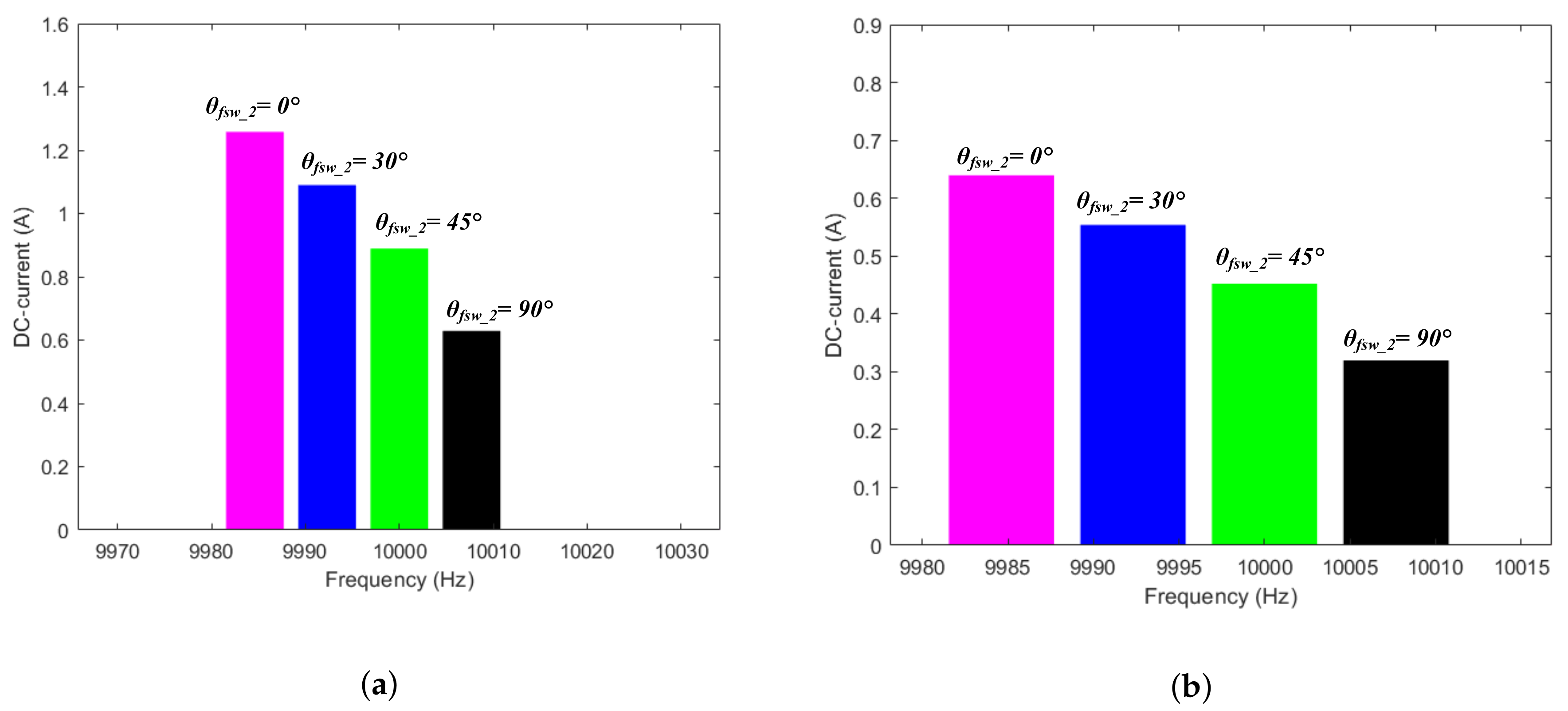
One of the ways to validate the effectiveness of the proposed harmonic mitigation strategy is to observe the switching frequency harmonics (i.e., at 10 kHz) for various carrier phase-shift angles in the
for the multi-converter system with a common DC-bank, and
for the multi-converter system with individual DC-banks. It is difficult to obtain these two wave-forms directly. Due to the presence of a large DC-link capacitor in the power stack, only low harmonics of
and
can be measured, as all higher harmonics are absorbed by the DC-capacitor. So, the CSV data for
and the capacitor current
were obtained from the oscilloscope measurements for the multi-converter system with a common DC-bank, and the harmonic spectrum was obtained in MATLAB. Similarly, for the multi-converter system with individual DC-banks, the CSV data for
and the capacitor current
were obtained from the oscilloscope measurements, and the harmonic spectrum was obtained in MATLAB. The obtained results are shown in
Figure 10a,b, respectively. It shows that the switching frequency harmonics (at 10 kHz) are at a minimum when a carrier phase-shift of
is applied for the proposed two multi-converter systems, making it the optimal carrier phase-shift angle. These results are, hence, in agreement with the proposed DC-link harmonic mitigation method explained in
Section 4.
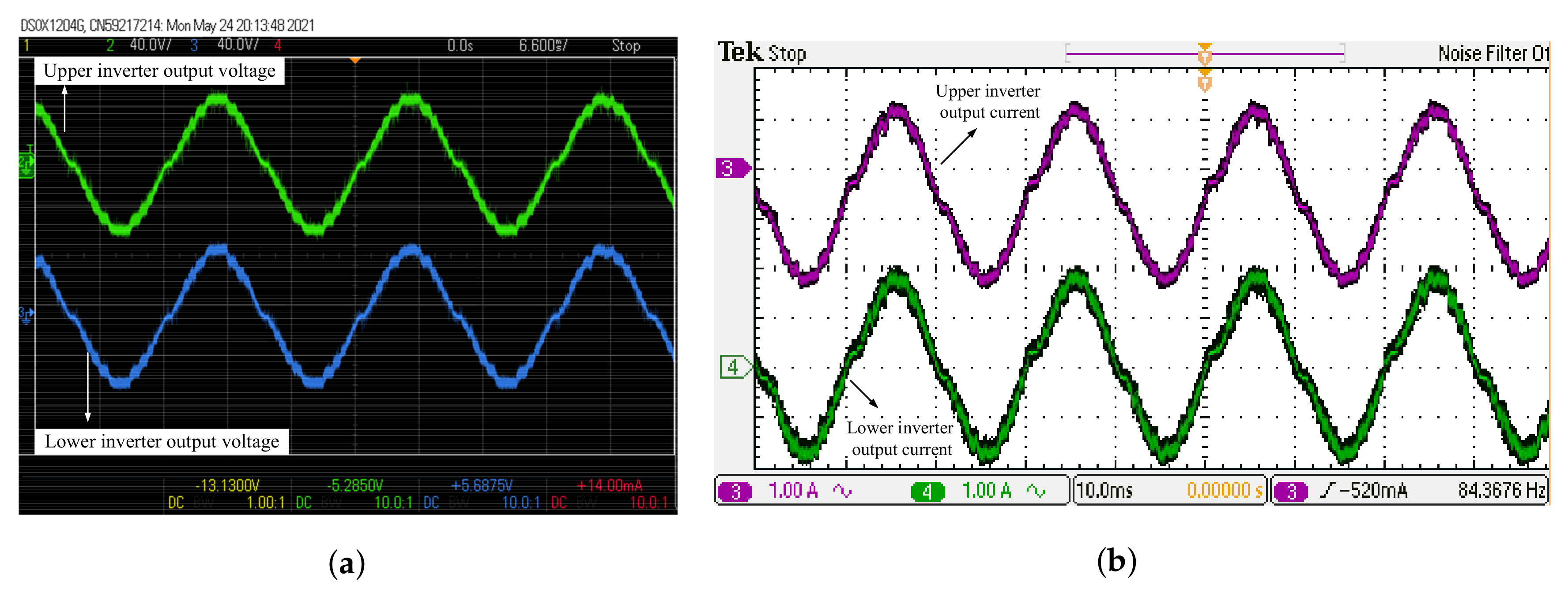
The output voltage and current waveforms at
and
for the multi-converter system with a common DC-bank captured in the oscilloscopes, are shown in
Figure 11. Since the output voltage and current waveforms are not affected by the phase-shift in carrier waves, they overlap each other at
and
6.2. DC-Harmonic Analysis Using Optimal Phase-Shift Angle for the Carrier Signal
To illustrate the DC-link harmonic mitigation method, the optimal phase-shift angle for the carrier signal (i.e.,
) is applied to both the topologies shown in
Figure 2 and
Figure 3. Each of the two inverters (of two topologies) is simulated (in PLECS) under a rated output power of 2.5 kW and have the same the rated operating conditions given in
Table 1. The effect of applying interleaving to the carrier signals of the parallel-connected inverters is illustrated in
Figure 12.
It can be seen that adopting the proposed method helps to reduce the dominant switching harmonic components (
= 40 kHz, 80 kHz, 120 kHz) in the DC-capacitor bank current, and the overall RMS capacitor bank current. As a result, the electro-thermal stress for each capacitor reduces, thereby increasing its life expectancy calculated using (5)–(12), as shown in
Table 7. From the industry point of view, it is important to have a lower DC-capacitor bank current as a lesser number of capacitors will be needed, which helps to lower the cost of the overall system.
However, it is necessary to take into consideration the fact that, from a practical application standpoint, it is almost impossible to achieve the loading of two drives according to operation at rated conditions [
29]. So, to further demonstrate the effectiveness of the proposed method under such scenarios, for the topologies shown in
Figure 2 and
Figure 3, the output load of the lower inverter is varied between 0 W and 2500 W (rated power), while the upper inverter is at a rated output power of 2500 W. In each case, the first (
= 40 kHz) and second switching frequency harmonic component (
= 80 kHz) are observed when
(conventional method) and
(proposed method) as shown in
Figure 13.
It is demonstrated in by
Figure 13a–d that, as the output power of the lower inverter (
) varies from 500 W to 2500 W, the first and switching frequency harmonic component amplitude reduces, due to the impact of the intervention of the carrier waves. The only time when there is no harmonic ripple cancellation is when
0 W, the scenario in which the lower inverter is not operating, due to which there is no interleaving (phase-shifting) occurring. Alternatively, the maximum ripple cancellation (or in other words, the minimum amplitude of switching frequency harmonic components) is achieved when each of the two inverters has the same output power (i.e., the case in which
2500 W in
Figure 13a–d. This is because, at the same output loading scenarios, the DC-ripples will be equal (due to the same output power) and opposite (due to
). Remarkably, even in cases where the inverters do not have the same output power (
is between 500 W and 2000 W), the DC-current harmonic (ripple) reductions occur. This result is of particular importance in industrial applications where parallel-connected inverters do not run at the same rated power. Applying the proposed method will help to reduce the harmonic content at the DC-link, thereby reducing the requirement to use a large number of DC-link capacitors (which saves costs).
Among the two topologies, the multi-converter system with individual DC-banks is preferred due to the flexibility it gives the industrial designers to play with the number of inverters being connected to the centralized rectifier, and also due to the better lifetime of its DC-link capacitors (
Table 7). Notably, one of the advantages of having a centralized rectifier is that, in the event of power failure, it is easy to connect a backup battery at the common DC link connecting the parallel inverter systems. Finally, in the future, it will also be possible to integrate renewable energy resources without much difficulty at the common DC link in these kinds of systems.
A few of the future works related to this paper include the following: a design approach to size the DC-link capacitor for the proposed topologies and compare how it is different from the DC-capacitor in the conventional multidrive systems. Further, more study needs to be conducted on how to optimise the phase-shift angles when two inverters have different speeds and different switching frequency waves, as well as different output frequencies. Including a greater number of inverters and then finding the optimal phase-shift angle in such scenarios can also be a topic for future work.


