1. Introduction
The Z-source inverter (ZSI), proposed in 2003, is a single-stage inverter with boost capability [
1]. The essential part of the ZSI is an impedance network placed at the dc side of the inverter bridge and composed of two capacitors, two inductors, and a diode. The impedance network combined with the additional shoot-through switching state (STS) enables the boost of the input dc voltage. The STS is achieved by short circuiting one or all the inverter legs during the zero switching states (ZSSs) of the utilized pulse width modulation (PWM) scheme. Many modifications and improvements have been proposed for the ZSI topology [
2,
3,
4], with the quasi-ZSI (qZSI) topology being one of the most commonly used [
5]. The main advantages of the qZSI are continuous input current and reduced voltage rating of one of the capacitors in the impedance network. This is achieved through different arrangement of the components in the impedance network.
The commonly utilized sinusoidal PWM (SPWM) and the space-vector PWM (SVPWM) require modifications to allow the STS injection. In [
6], the most common qZSI-compatible SVPWM methods are presented. They differ by the number of the STS occurrences within a single switching period, ranging from two to six. There are also many modifications of the SVPWM method which aim to improve the performance of different ZSI topologies. For example, the main goal of the method proposed in [
7] was to reduce the switching losses, whereas in [
8] the main goal was to reduce the common-mode voltage. The main advantage of the SVPWM with regard to the SPWM is the higher achievable ac voltage at the inverter bridge output for a given input dc voltage. However, this disadvantage of the SPWM may be overcome by injecting 1/6 of the 3rd harmonic component into the respective reference signals [
9]. Among the SPWM-based methods most commonly applied for the ZSI topologies are the simple-boost control (SBC), the maximum boost control (MBC) [
10], and the maximum constant boost control (MCBC) [
11,
12]. All the mentioned methods imply that the value of the STS duty ratio (
D0), which is defined by the duration of the STS and the switching period, cannot be varied independently of the amplitude modulation index (
Ma). This represents a significant disadvantage in terms of the control of the ZSI-related inverters in certain applications [
13,
14,
15,
16,
17]. Therefore, the methods utilized in [
13,
14,
15,
16,
17] allow
D0 value to vary regardless of the
Ma value as long as
D0 value is lower than the maximum allowed, which is, in turn, defined by the applied
Ma [
11]. However, in the literature, the start of the STS is typically not synchronized with the start of the ZSS, except for the case of the MBC method. This results in additional ZSSs with respect to the case when the STS and ZSS would start simultaneously, leading to additional switching losses. In the conventional approach, utilized in [
15,
16], the STS signal is generated based on the comparison of two dc reference signals (positive and negative) with the carrier signal. However, in this case, the start of the STS is not synchronized with the start of the ZSS.
The STS injection into standard PWM schemes sometimes requires modifications in terms of the utilized hardware [
18,
19,
20,
21,
22]. The STS implies short circuiting of the inverter phase legs, which is forbidden in the conventional voltage-source inverters (VSI) because it leads to the dc-link short circuit and, ultimately, to the inverter failure. Therefore, some microcontrollers, such as the MicroLabBox (dSpace) utilized in [
18] and in this paper, do not allow the implementation of the STSs in the dedicated PWM blocks. One of the solutions is the introduction of the additional circuitry, as in [
18,
19,
20,
21,
22], composed of the logic OR gates. Another is to impose the STSs by utilizing two different reference signals for the PWM pulses generation of two transistors from the same inverter leg [
23,
24]. However, the latter implies a high current ripple rating (approximately 130% of the mean value) of the impedance network inductors [
23].
The conventional VSIs require the introduction of dead-time into the SPWM pulses in order to prevent short circuiting during the SPWM switching transitions, caused by the non-ideal switching of the involved transistors [
25]. On the other hand, in the case of ZSI topologies, the introduction of the dead-time is not necessary due to the existence of the impedance network on the dc side of the inverter bridge [
26,
27]. However, by omitting the dead-time, a sporadic, unintended short circuiting is bound to occur across the inverter legs due to the aforementioned reason (as would be the case in the conventional VSIs if the dead-time was not introduced). Although these states would not cause the ZSI failure, they would result in an additional, unintended voltage boost. This phenomenon is more prominent at higher values of the inverter bridge input voltage due to the longer duration of the PWM switching transitions. To our best knowledge, in terms of ZSI-related topologies, only in [
28] the dead-time was implemented in order to prevent unintended short circuiting across the inverter legs of the multi-level ZSI. In this case, the implementation of the dead-time caused the increase of a common-mode voltage which was reduced by means of the proposed SVPWM scheme. The reason for omitting the dead-time in the literature may be the fact that the peak value of the input voltage (with neglected overshoot) of an inverter bridge utilized in [
1,
5,
7,
8,
10,
12,
13,
14,
15,
16,
17,
19,
20,
21,
22] was relatively low (approximately 500 V), so this phenomenon was not that prominent.
This paper presents a novel method of the STS injection into the three-phase SPWM and it is organized as follows. In
Section 2, the basic theoretical background of the qZSI is provided.
Section 3 presents the novel STS injection method, called the zero-sync method, in which the starts of the STSs and the ZSSs are synchronized. In this way, compared to the conventional STS injection method, the total number of switchings in the inverter bridge within a single period of the sinusoidal reference signal is reduced by approximately four times the frequency modulation index (
Mf). In
Section 4, the additional circuitry required for the implementation of the zero-sync method is described. This circuitry detects the ZSS from the input SPWM pulses generated by a microcontroller and injects the STS pulses of adjustable, predefined duration into the SPWM pulses. In
Section 5, a comparison of the zero-sync method and the conventional STS injection method is carried out by utilizing the laboratory setup of the three-phase qZSI in the stand-alone mode. The comparison is carried out for six values of the switching frequency from 5 kHz to 10 kHz and three values of the load power from 1000 W to 3000 W. The peak value of the voltage across the inverter bridge (with neglected transient overshoot) is varied in the range of 500–1200 V. In
Section 6, the minimal necessary dead-time is additionally introduced to prevent unintended short circuiting across the inverter legs caused by the non-ideal switching of the involved transistors and, hence, to avoid the additional, uncontrollable voltage boost. Finally, in
Section 7, the experimental results are discussed, whereas in
Section 8 the conclusions are presented.
3. Analysis of a Zero-Sync Shoot-Through State Injection Method
The main features of the zero-sync method are the injection of the STS right at the beginning of each ZSS and the control of the STS duration by means of the timer. The value of the maximum allowed STS duty ratio (
D0,max) is selected to be the same as for the maximum constant boost control (MCBC) with injected 3rd harmonic, as follows [
11]:
This ensures that the STS lasts equal or less than the ZSS, while achieving a time-invariant boost of the inverter, corresponding to the applied
D0 value in the range 0 <
D0 <
D0,max. The best way to describe the zero-sync method is by considering the corresponding waveforms.
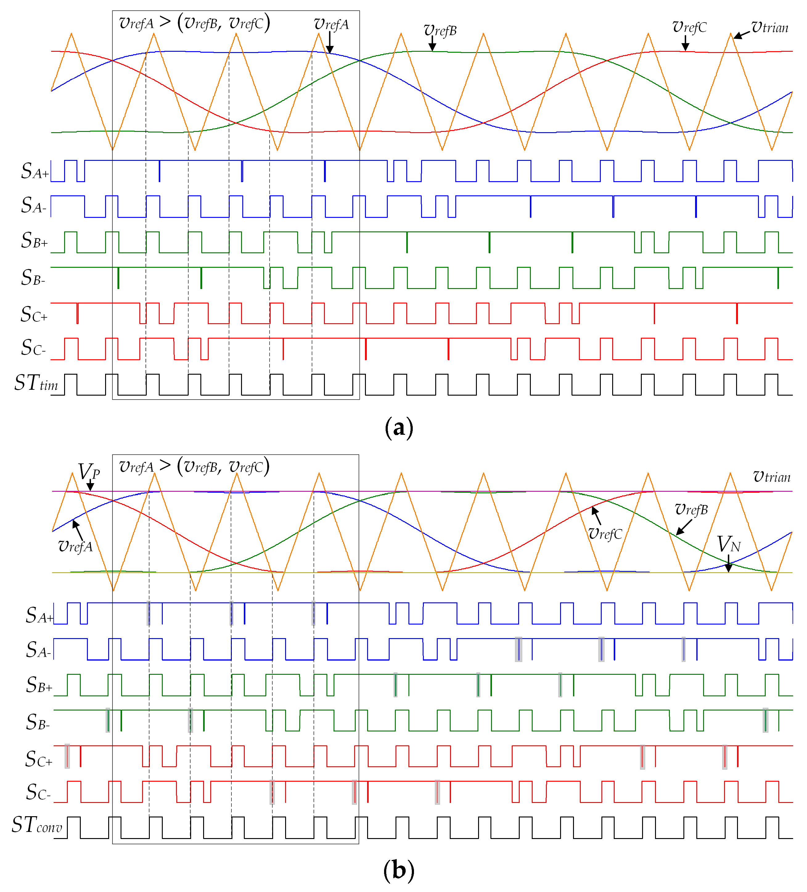
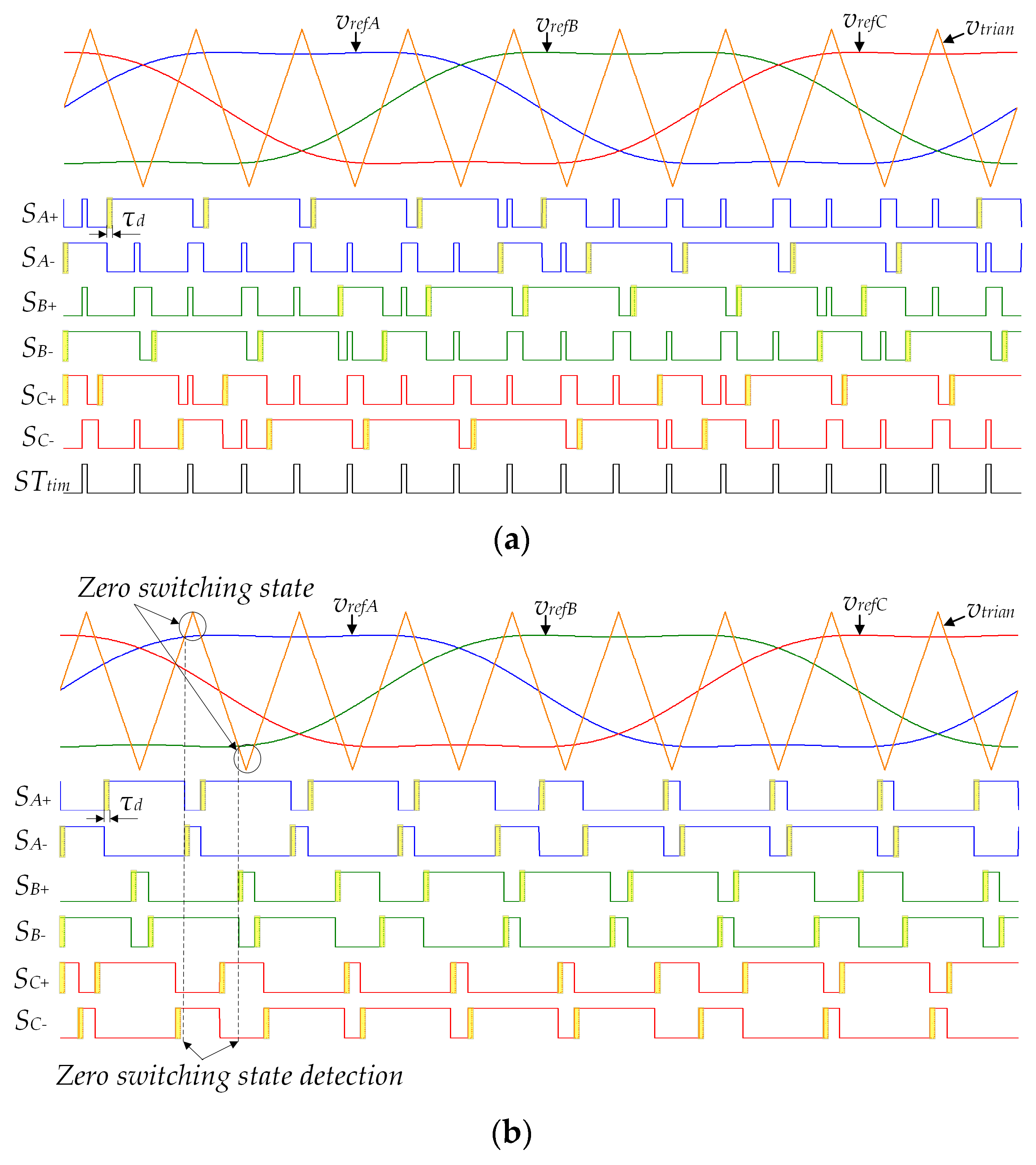
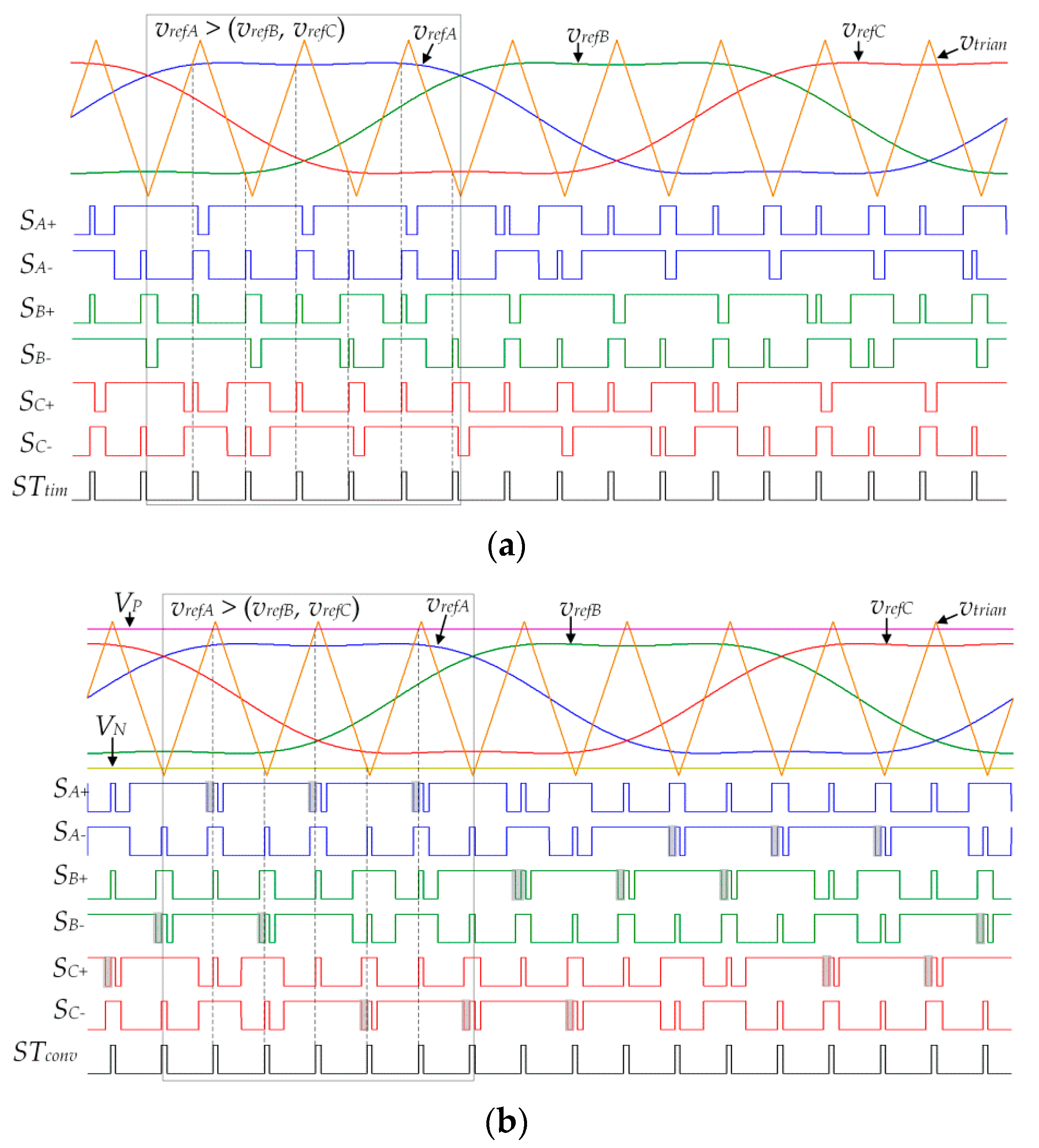
Figure 2a shows the waveforms of the reference voltages (
vrefA,
vrefB,
vrefC), the carrier triangular signal (
vtrian), the STS signal (
STtim), and the SPWM pulses of all the transistors (
SA+,
SA−,
SB+,
SB−,
SC+,
SC−), with 0 <
D0 <
D0,max. The STSs occur right at the beginning of each ZSS (denoted by dashed lines). During the STSs, the pulses of all the transistors are set to 1, which means that they all conduct.
The STS injection method considered in
Figure 2b is the conventional method [
15,
16]. In this method, the STS signal (
STconv) is obtained as a result of comparison of the reference dc voltages
VP and
VN with
vtrian. The
STconv value is equal to 1 in the case when
vtrian >
VP or
vtrian <
VN, otherwise it is equal to 0.
There are notable differences in the switching states distribution between the two STSs injection methods shown in
Figure 2, although the same values of
Ma and
D0 were applied for both the methods. This phenomenon is analyzed for the corresponding transistor pulses of the phase A, where the same conclusion may be reached by considering the other two phases. The differences exist in the upper transistor pulse (
SA+) during the interval where the instantaneous value of
vrefA is higher than the values of
vrefB and
vrefC. In that interval, the switching states of the transistor for the zero-sync method occur in the following order: the active state, the STS, and the ZSS. On the other hand, in the same interval, the conventional method utilizes switching states in the following order: the active state, the first ZSS, the STS, and the second ZSS. Consequently, the conventional method utilizes the additional ZSS depicted by the shaded surfaces in
Figure 2b. This additional switching state implies two additional switching transitions of the transistor: the turn-off transition from the active state into the ZSS, and the turn-on transition from the ZSS into the STS. The number of the additional switching transitions increases with the frequency modulation index, which is defined as the ratio between the switching frequency (
fsw) and the fundamental frequency of the reference voltages (
f). The described additional transitions also occur in the lower transistor pulse (
SA−) during the interval when the instantaneous value of
vrefA is lower than the values of
vrefB and
vrefC. Finally, compared to the conventional method, in the zero-sync method, each transistor in the inverter bridge utilizes two switchings less per switching period during one third (2π/3) of the fundamental period of the reference signal. Consequently, the total number of switchings in the inverter bridge during each fundamental period (1/
f) is reduced by
It is determined that
Nred calculated according to (4) corresponds to the actual number of reduced switchings when the amplitude modulation index
Ma is equal to or greater than 1 or
Mf is the integer multiple of 3. Otherwise,
Nred calculated by (4) is slightly lower (i.e., by up to five) than the actual number of reduced switchings. However, this is a negligible error given that
Mf in common applications varies from 50 to 500 [
29].
As a result of the reduced switching, the switching losses are lower in the case of the zero-sync method, whereas the conduction losses remain the same since the total duration of the ZSS within each Tsw is the same for both the considered methods.
An increase of the
D0 value, with the applied constant
Ma, would lead to a shorter duration of the additional ZSS. Therefore, the question arises whether the additional ZSS would disappear if
D0 would reach
D0,max. The answer to this is provided in
Figure 3, where the same waveforms as in
Figure 2 are shown for the case
D0 =
D0,max.
Figure 3 proves that the additional ZSS still exists even in this case, although its duration is very short. Finally, it may be concluded that the difference in the switching states distribution between the zero-sync method and the conventional method always exists, regardless of the
D0 value.
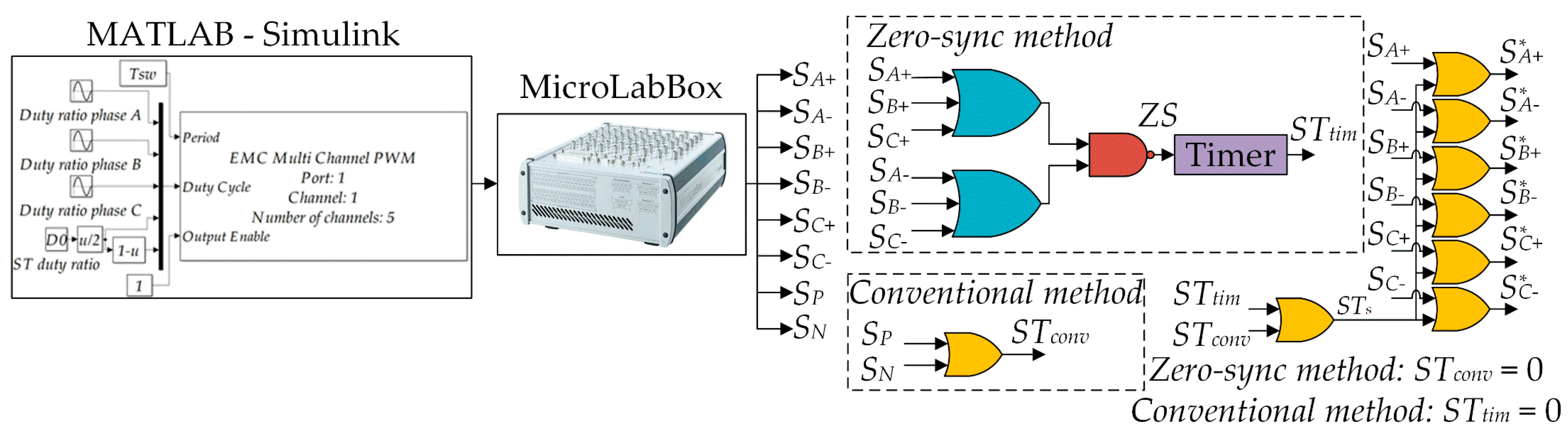
4. Hardware Implementation
The logic diagram of the PWM pulses generation with the STS injection for both the zero-sync and conventional methods is shown in
Figure 4. The SPWM pulses are generated by means of the MicroLabBox (dSpace) microcontroller, whereas the corresponding control algorithm was built in the Matlab-Simulink. As for the zero-sync method, the ZSSs are detected by considering all the SPWM pulses. The logic signal (
ZS) shown in
Figure 4 equals 1 during the zero SPWM state, otherwise it equals 0. The SPWM pulses for the upper transistors (
SA+,
SB+,
SC+) and those for the lower transistors (
SA−,
SB−,
SC−) are fed into the respective OR gates. The output signals of the two OR gates are fed into the NAND gate, which, in turn, generates the
ZS signal at its output. The
ZS value for all the possible combination of the SPWM pulses is given in
Table 1. It is notable that the
ZS signal may be correctly obtained by utilizing a single logic XNOR gate for the upper transistor signals (
SA+,
SB+,
SC+) or the lower transistors signals (
SA−,
SB−,
SC−). However, this method was not utilized due to the later introduction of the dead-time, as described in
Section 6. The rising pulse of
ZS (i.e., from 0 to 1) initiates the timer: the logic STS signal (
STtim) is set to value 1, which marks the start of the STS. The duration of the STS is equal to half of the STS period (
T0/2). At the end of the STS, defined by the timer operation,
STtim becomes 0 and retains that value until the next STS. As for the conventional method, the corresponding logic STS signal (
STconv) is the result of the logic OR operation of the signals
SP and
SN, which are obtained as the result of comparison of the reference voltages
VP and
VN with
vtrian. The STS signal
(STs), which is in the end injected into the six SPWM pulses by means of the respective logic OR gates, is the result of the logic OR operation of the signals
STtim and
STconv. However, it is important to note that when the zero-sync method is implemented,
STconv is permanently set to zero. Likewise, when the conventional method is implemented,
STtim is permanently set to zero. The output PWM pulses (
S*A+, S*A-, S*B+, S*B−, S*C+, S*C−) are, in fact, the SPWM pulses with the injected STSs.
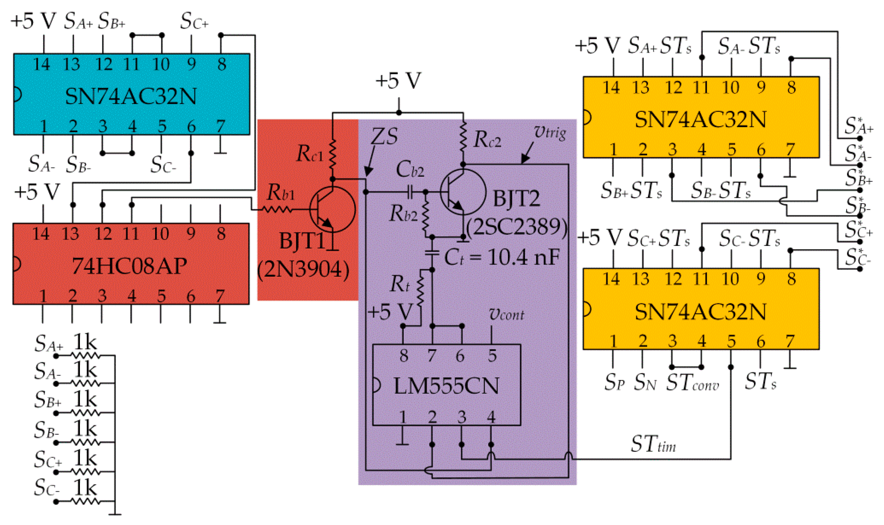
Figure 5 shows the electrical scheme of the circuitry utilized for the STS injection by means of both the considered methods. The circuitry was built based on the logic diagram, so the colors of the components in
Figure 5 correspond to those in
Figure 4. The logical 0 in the logic diagram corresponds to 0 V in the electrical circuitry, whereas the logical 1 corresponds to +5 V. The supply voltage of the circuitry (
Vcc) was set to +5 V. The
ZS signal required for the implementation of the zero-sync method is generated by the means of the logic OR gates SN74AC32N (Texas Instruments) along with the logic AND gate 74HC08AP (Texas Instruments) and the logic inverter. The latter is realized by utilizing the NPN bipolar junction transistor (BJT1) 2N3904 (Texas Instruments). The resistors
Rb1 = 10 kΩ and
Rc1 = 1 kΩ shown in
Figure 5 are utilized in the base and collector circuit of the BJT1, respectively, to ensure adequate BJT1 currents.
A monostable operation mode of the timer LM555CN (Texas Instruments) is implemented in order to ensure desired half STS period (T0/2) in the zero-sync method. In this operation mode, the timer output (pin 3), which is utilized as the signal STtim, is set to +5 V in the case when the voltage value of 0 V is applied to the trigger input (pin 2). The trigger input signal (vtrig) is generated by utilizing the NPN BJT2 2SC2389 (Rohm). At the beginning of the ZSS, the BJT1 turns off which causes the ZS value to become +5 V. The current instantaneously starts to flow from the supply terminal (+5 V) through Rc1 and Cb2 = 100 pF into the base of the BJT2. That initiates the start of Cb2 charging and the BJT2 turns on (note that Rc2 = 5.6 kΩ ensures adequate BJT2 collector current), which results in vtrig = 0 V. This triggers the timer and the STtim value changes to +5 V, which represents the start of the STS. As a result, the timer pins 6 and 7 internally disconnect from the pin 1, which is connected to the ground. Therefore, the capacitor Ct, connected between the timer pins 6 and 7 and the ground, begins to charge through the resistor Rt, connected between the timer pins 8 (supply +5 V) and 6 and 7. During the STS, the vtrig value remains 0 V as long as the base current is high enough to maintain the BJT2 turned on, practically until Cb2 is fully charged. Once Cb2 is fully charged, the BJT2 turns off and the vtrig value becomes +5 V. In the considered circuitry, the vtrig value remains 0 V for approximately 1.5 μs within each ZSS, which is determined by the time constant Rc1Cb2 and BJT2 parameters such as the base-collector voltage and the current transfer ratio of the base current. The value of the timer output (STtim) remains +5 V until the voltage across Ct (vCt) reaches the value of the signal applied to the timer pin 5 (vcont). At that point, the STtim value becomes 0 V (STS ends) and retains that value until the next STS. As the STtim value changes to 0 V, the timer pins 6 and 7 internally connect to the pin 1 (ground) and thus enable Ct discharge. Note that for the proper operation of the timer, the vtrig value has to be +5 V at the moment when vCt reaches vcont. Therefore, each STS generated by the timer in considered circuitry has to last longer than 1.5 μs. Finally, at the end of the ZSS, the BJT1 turns on, the ZS value changes to 0 V, and Cb2 discharges through Rb2 = 10 kΩ and BJT1. In this way, the multiple trigger occurrences within a single ZSS are prevented. The implemented circuitry allows the STS to last equal or lower than the ZSS. This is achieved by utilizing the ZS signal to control the reset of the timer (pin 4). If the reset is set to 0 V, the timer output is disabled (pin 3 is permanently set to 0), whereas if the reset is set to +5 V, the timer operates regularly.
The STS signal (
STs) shown in
Figure 5 is injected into the SPWM signals by means of the logic OR gates SN74AC32N.
STs is the result of the logic OR operation of
STtim and
STconv.
STconv is generated as the result of logic OR operation of
SP and
SN, also by utilizing the logic OR gates SN74AC32N. Note that when the zero-sync method is implemented, the values of
SP and
SN are permanently set to 0 V, whereas when the conventional method is implemented, the
vcont value is permanently set to 0 V. Finally, it is important to emphasize that the rise times of the logic gates and the timer of approximately 10 ns and 100 ns, respectively, do not affect the proper operation of the circuitry.
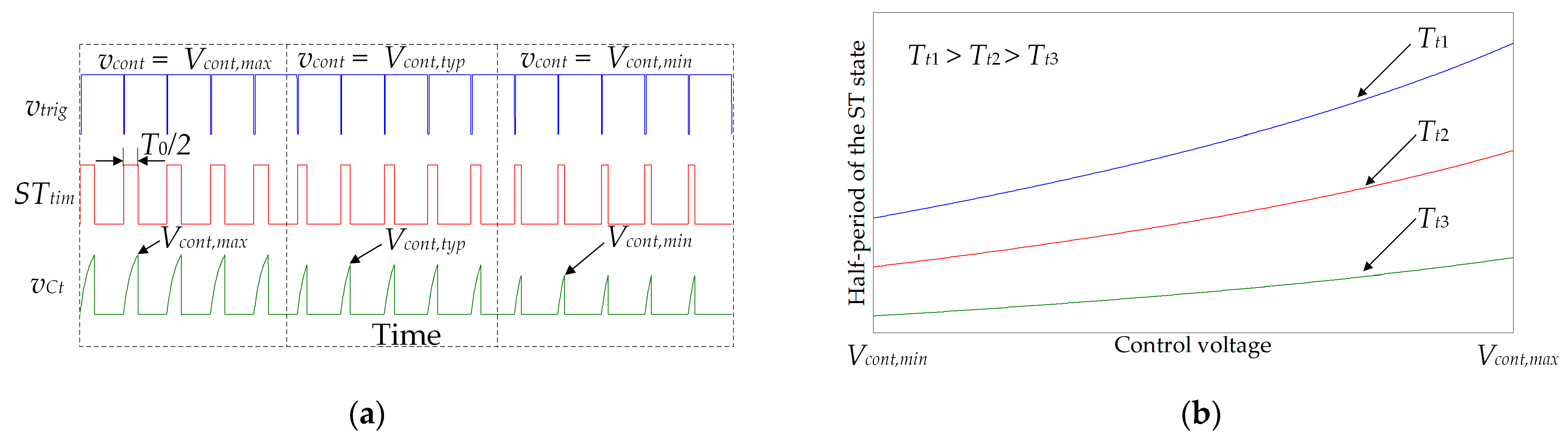
Figure 6a shows the waveforms of
vtrig,
STtim, and
vCt in the case when the maximum (
Vcont,max), minimum (
Vcont,min), and typical (
Vcont,typ) values of
vcont are applied, with constant values of
Rt and
Ct. These three values of
vcont, selected to point out the effect of
vcont variation, are defined based on the recommendations given in the datasheet of the timer manufacturer. However,
vcont may be varied continuously, with the precision depending on the resolution of the MicroLabBox analog output. The value of
vCt may be calculated based on the supply voltage and the time constant
Tt =
RtCt, as follows:
In the considered monostable mode, the
STtim value instantly changes from 1 to 0 when
vCt reaches
vcont. Hence, the value of
T0/2 may be calculated based on (5), with applied
vCt =
vcont, as follows:
In this study, the value of
Vcc is set to 5 V which results with
Vcont,max = 4 V and
Vcont,min = 2.6 V according to the recommendations given in the datasheet of the timer manufacturer. By considering the values of
Vcont,min and
Vcont,max, the maximum (
T0,M−tim/2) and minimum (
T0,m−tim/2) values of
T0/2 may be defined as follows:
The scope of
T0/2 variation depends on the value of the time constant (
Tt), wherein the
T0,m−tim/2 value has to be higher than 1.5 μs, as explained before.
Figure 6b shows
T0/2 as a function of
vcont for different values of
Tt. The minimum and maximum values of
T0/2, which may be achieved by the timer, define the scope of the STS duty ratio variations. The minimum (
D0,m−tim) and maximum (
D0,m−tim) duty ratios are defined as follows:
Hence, due to fact that the range of
D0 variation is limited according to (8), all
D0 values in the range of 0 to
D0,max may not be achieved by utilizing the timer. This is not a huge disadvantage since in most applications such a broad scope of
D0 is not required [
13,
14,
15,
16,
17]. In order to achieve the desired scope of
D0 variation for the certain value of
Tsw, the value of
Tt has to be determined from (8).
Note also that the described electrical circuitry allows the implementation of the SPWM with omitted STSs. To achieve that, the values
vcont,
SP, and
SN have to be permanently set to 0 V. In this way, the considered electrical circuitry does not generate the STSs. The described electrical circuitry also allows the implementation of the simple-boost SVPWM method, proposed in [
7].
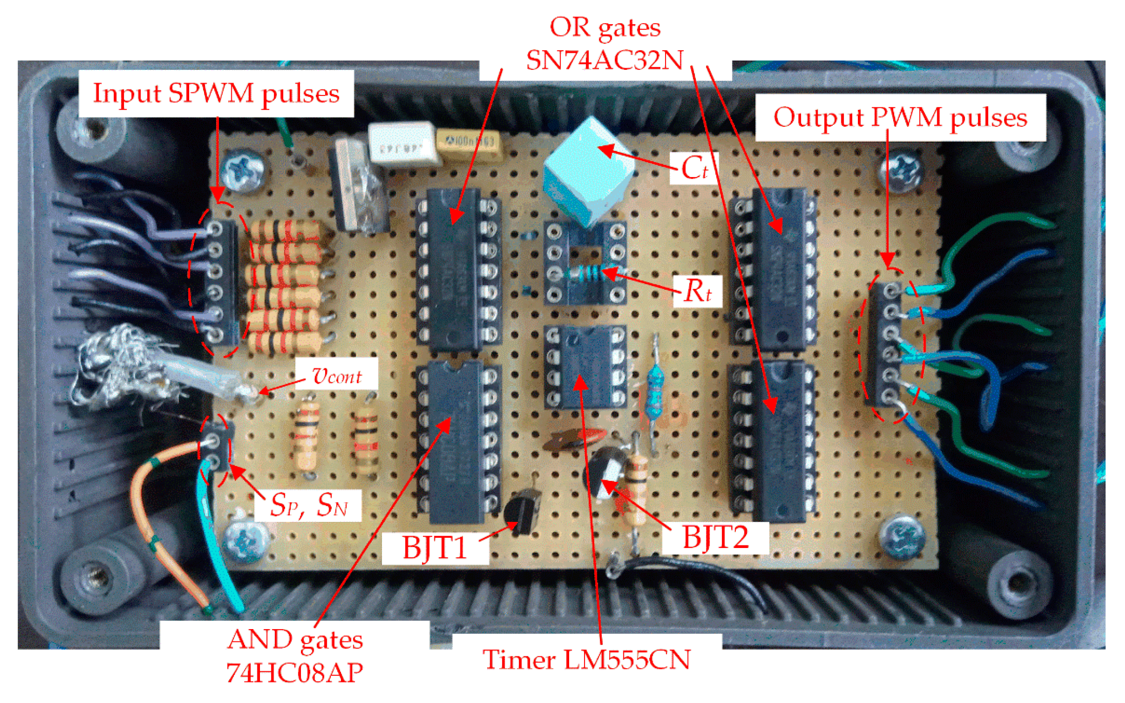
Figure 7 shows the photo of the electrical circuitry whose electrical diagram is shown in
Figure 5. The input SPWM pulses along with the signals
SP and
SN are connected to the digital output ports of the MicroLabBox, whereas the output PWM pulses are connected to the gate drivers of the transistors. The control voltage (
vcont) is connected to the board from the analog output of the MicroLabBox by means of a coaxial cable. Note that
Ct is fixed to the board, whereas
Rt may easily be removed and replaced by the resistor of another resistance value. Thus, the desired value of
Tt, which ensures the desired scope of
D0 variation, is achieved by applying
Rt with the required resistance value to the board. In order to prevent problems with the dirty ground, the ground pins of all the logic gates are connected to the copper plate placed underneath the main board. Moreover, the electromagnetic interference (EMI) was suppressed by accommodation of the board into the housing BIM2001/11-EMI/RFI (Camdenboss).
5. Experimental Evaluation of the Zero-Sync Method
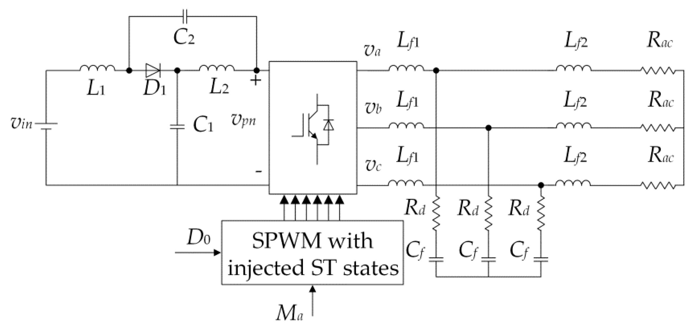
Figure 8a shows the laboratory setup of the system used for the experimental evaluation of the zero-sync method. The main components are denoted as follows:
DC power supply Chroma 62050H 600S, voltages up to 600 V, currents up to 8.2 A.
Hall-effect transducers LA 50-P/S55 (for the qZSI input current and the output phase current), DVL 500 (for the qZSI voltages), and CV 3–500 (for the ac load voltage) (LEM).
Power analyzer Norma 4000 (Fluke), used for the measurement of the output load power.
qZSI impedance network built of inductors with powder cores T520-26 (Micrometals) (L1 = L2 = 20.2 mH (unsaturated), RL = 0.5 Ω (at 25 °C)), polypropylene capacitors MKSPI35-50U/1000 (Miflex) (C1 = C2 = 50 μF, ESR = 7.8 mΩ), and the diode which was built as a serial compound of three diode sets, where each set was built as a parallel compound of three FWDs of the IGBT-FWD pair IRG8P25N120KD (International Rectifier).
qZSI three-phase inverter bridge (IXBX75N170 IGBTs (IXYS) and SKHI 22B(R) drivers (Semikron)) shown in
Figure 8b.
LCL filter at the qZSI output stage (Lf1 = 8.64 mH, Lf2 = 4.32 mH, Cf = 4 μF, Rd = 10 Ω).
Variable resistors utilized as a symmetric three-phase load.
MicroLabBox controller board (dSpace) for the qZSI control.
Oscilloscope MDO 3014 (Tektronix).
The considered laboratory setup was built to operate in the stand-alone configuration with the switching frequencies in the range 5–10 kHz. The selected IGBTs, shown in
Figure 8b, have a sufficiently high collector-emitter break down voltage and nominal collector current to ensure proper operation of the qZSI. They were utilized instead of metal oxide semiconductor field effect transistors (MOSFETs) due to the lower level of electromagnetic interference [
30]. On the other hand, IGBTs have somewhat higher switching losses compared to MOSFETs. The impedance network diode was built as the above-described series-parallel combination of six FWDs of the IGBT-FWD pair IRG8P25N120KD (International Rectifier), thus reducing both the current and voltage stress of the FWDs. The values of the inductors and capacitors in the symmetric impedance network have been chosen to ensure acceptable inductor current ripple in the considered switching frequency range. As for the output LCL filter, the value of the capacitors has been chosen in order to keep the reactive power under 5% of the nominal inverter power of 4 kW. The values of the damping resistances (
Rd), required to avoid the resonance, have been chosen according to the recommendations in [
31]. The value of the LCL filter inductors has been chosen in order to ensure acceptable THD of the inverter output current.
The control algorithm of the qZSI was executed with the sampling frequency of 10 kHz. The qZSI was operated in the open-loop mode, meaning that the RMS value of the fundamental load phase voltage was not controlled, whereas its frequency was set to 50 Hz by means of the SPWM. All the experiments were carried out with the three-phase resistive load connected to the inverter output.
The values of D0,max and Ma utilized during the measurements were determined according to the MCBC method and the maximum allowed value of Vpn. The maximum Vpn value of 1200 V was selected in order to avoid high levels of the electromagnetic interference, disrupting the normal operation of the gate drivers. The maximum applied qZSI input voltage amounted to 500 V, which along with Vpn = 1200 V defines D0,max = 0.29 according to (2). Finally, the Ma value of 0.819 is obtained according to (3). For the Ma value higher than 0.819, the Vpn value would surpass 1200 V for the corresponding D0,max value, whereas for the Ma value lower than 0.819, the Vpn value would stay below 1200 V for D0 in the range 0 < D0 < D0,max.
The switching frequencies in the range 5–10 kHz were considered during the measurements.
Rt values of 1 kΩ and 2 kΩ were utilized with
Ct fixed to 10.4 nF in order to ensure the desired values of
T0/2 for all the considered switching frequencies.
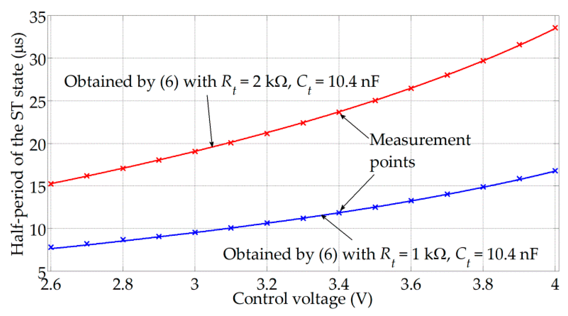
Figure 9 shows
T0/2 as a function of the control voltage (
vcont) for the two utilized values of
Rt. It is notable that the experimentally measured values of
T0/2 almost perfectly match those obtained by (6) for both the considered resistance values.
Table 2 shows the available range of variation of the duty ratio value, as per (8), for all the considered switching frequencies and for the two applied
Rt values.
The experimental evaluation of the zero-sync method was carried out through the comparison with the conventional method. First, the respective waveforms were compared in order to highlight the differences in the switching states distribution between the two considered methods.
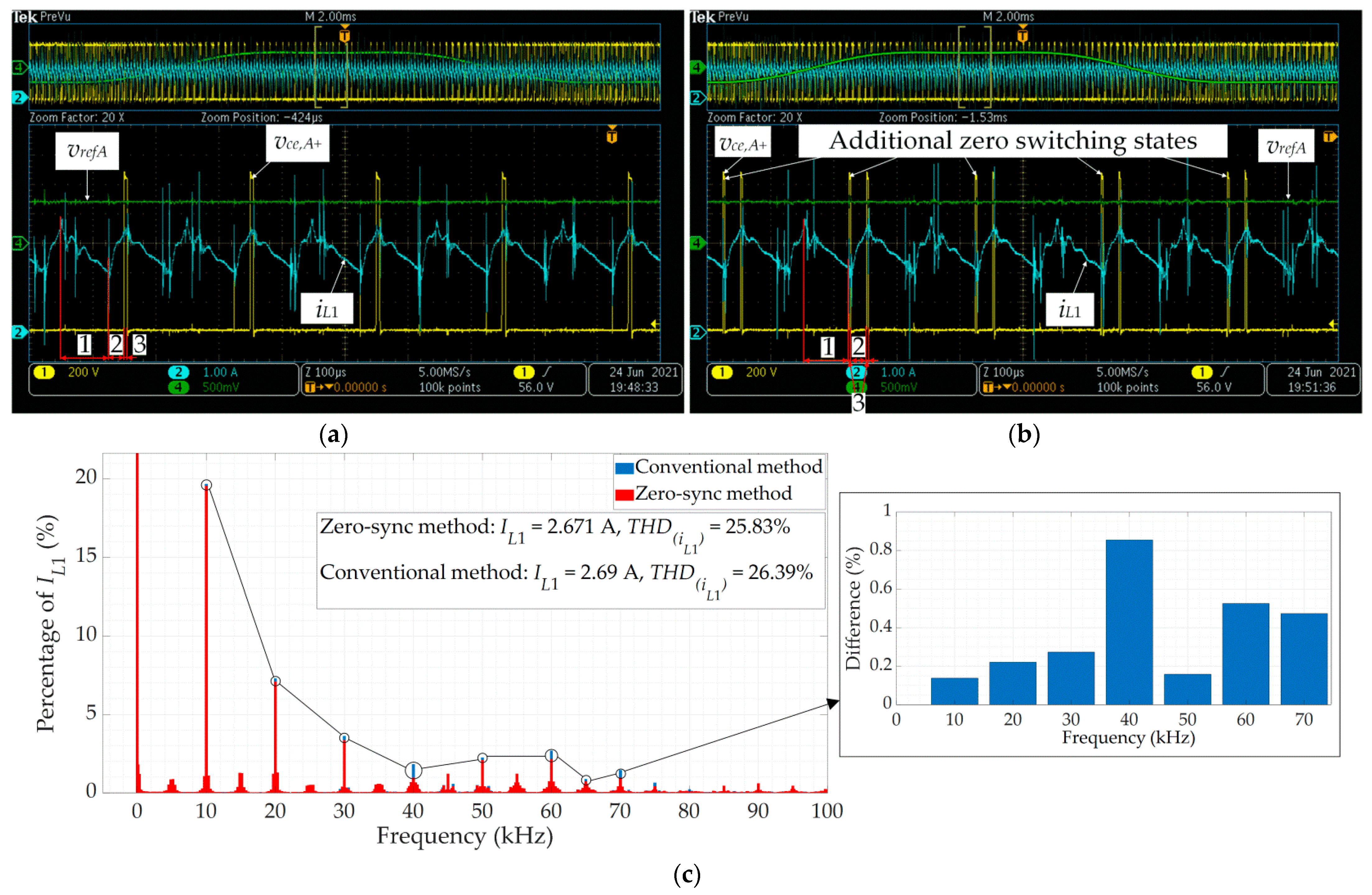
Figure 10a,b show the respective experimental waveforms of the collector-emitter voltage of the upper transistor in the phase A (
vce,A+), the qZSI input current (
iL1), and the reference voltage in the phase A (
vrefA) for a single fundamental period of
vrefA. The measurements were carried out with
fsw = 5 kHz,
D0 = 0.24,
Ma = 0.819,
vin = 500 V, and the load power set to 1000 W. The waveforms were recorded by the oscilloscope MDO 3014 (Tektronix). The part of the
vrefA period with notable differences between the two considered injection methods is additionally magnified (lower part of
Figure 10a,b). The transistor switching state may be detected based on the value of
vce,A+: when
vce,A+ value is approximately 0, the transistor is turned on, whereas it is turned off otherwise. On the other hand, the
iL1 waveform was utilized for the detection of the STSs: during the STS,
iL1 increases, whereas it decreases otherwise. The inductor current ripple for both the considered methods is practically the same and amounts to approximately 46% of the mean value. The calculated value of the current ripple obtained as
—the equation given in [
15]—amounts to 37% of the mean value. The
VC1 value of approximately 770 V was determined according to the corresponding waveforms shown in
Figure 11, whereas the inductance value was determined according to the equation given in [
32], which is based on the mean value of the inductor current (
IL1).
The switching states of the zero-sync method are shown in
Figure 10a and occur in the following order: the active state (interval 1), the STS (interval 2), the ZSS (interval 3). As opposed to this, the conventional method, shown in
Figure 10b, utilizes an additional ZSS (
vce,A+ ≈ 800 V) in between the active state and the STS. This proves the fact mentioned in
Section 3 that the conventional method utilizes the additional ZSS for the transistor A+ (two additional switching transitions) in the interval where
vrefA > (
vrefB,
vrefC) applies (similar applies for all the other transistors as well).
Figure 10c shows the harmonic spectrum of the qZSI input current waveform for both the considered methods, where harmonic components are shown as the percentage of the input current dc component. The harmonic components that are integer multiples of 2
fsw = 10 kHz are notable since the fundamental frequency of the ac component of the qZSI input current amounts to 2
fsw (i.e., there are two STSs per switching period). The share of high-order harmonics and the THD are lower in the case of the zero-sync method compared to the conventional method.
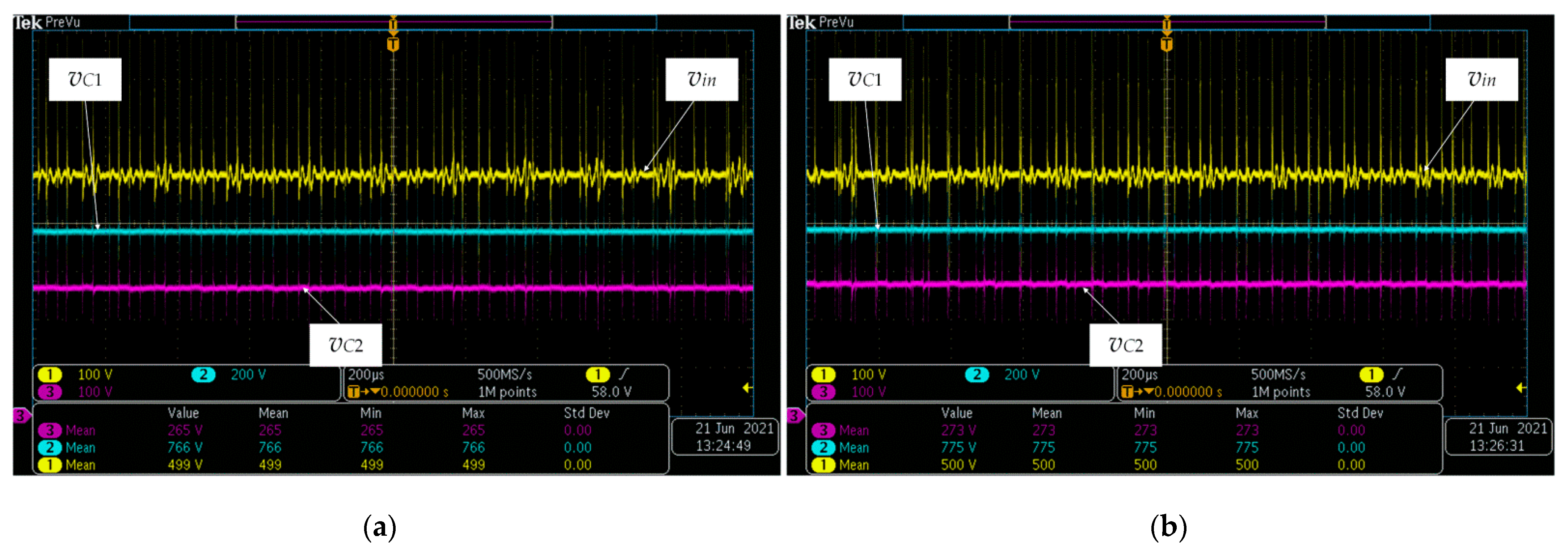
The waveforms of the qZSI input voltage and the voltages across the capacitors
C1 and
C2 for both the considered methods are shown in
Figure 11. The measurements were carried out with the same input parameters as the measurements shown in
Figure 10. The waveforms of all the considered voltages are similar for both the considered methods. However, note that the mean values of the voltages
vC1 and
vC2 (
VC1 = 766 V,
VC2 = 265 V for the zero-sync method and
VC1 = 775 V,
VC2 = 273 V for the conventional method) are higher than the values obtained from (2) based on
vin and
D0 (
VC1 = 731 V,
VC2 = 231 V). This is the consequence of the unintended additional boost. This, in turn, occurs due to the unintended short circuiting across the inverter legs (i.e., unintended STSs) caused by the non-ideal switching of the involved transistors, as discussed later. Likewise, the mean values of
vC1 and
vC2 are higher for approximately 10 V in the case of the conventional method compared to the zero-sync method due to the higher overall number of switchings and, consequently, higher number of unintended STSs. This unintended additional boost was eliminated by introducing the dead-time, which is shown in the next section.
Based on the waveforms shown in
Figure 10 and
Figure 11, it may be concluded that there are no notable differences in terms of the EMI noises between the two considered methods. In order to achieve a satisfying trade-off between the EMI noises and the switching losses of the IGBTs, the gate turn-on and turn-off resistances were both set to 15 Ω. Detailed analysis of the EMI noises exceeds the scope of this study, but it may be assumed that the EMI noises are somewhat lower in the case of the proposed zero-sync method due to the lower overall number of switchings compared to the conventional method.
The difference in the switching states distribution between the two considered STS injection methods results in the inverter losses difference and, thus, the efficiency difference. For the purpose of inverter losses and efficiency measurement, the inverter input power was measured by Chroma, whereas the output load power was measured by the high-precision power analyzer Norma 4000 (Fluke). The inverter losses (
Pl−zsm/conv) for the zero-sync method (subscript “
zsm”) and the conventional method (subscript “
cm”) were obtained as
where
Pin−zsm/cm is the inverter input power and
Pout−zsm/cm is the load power.
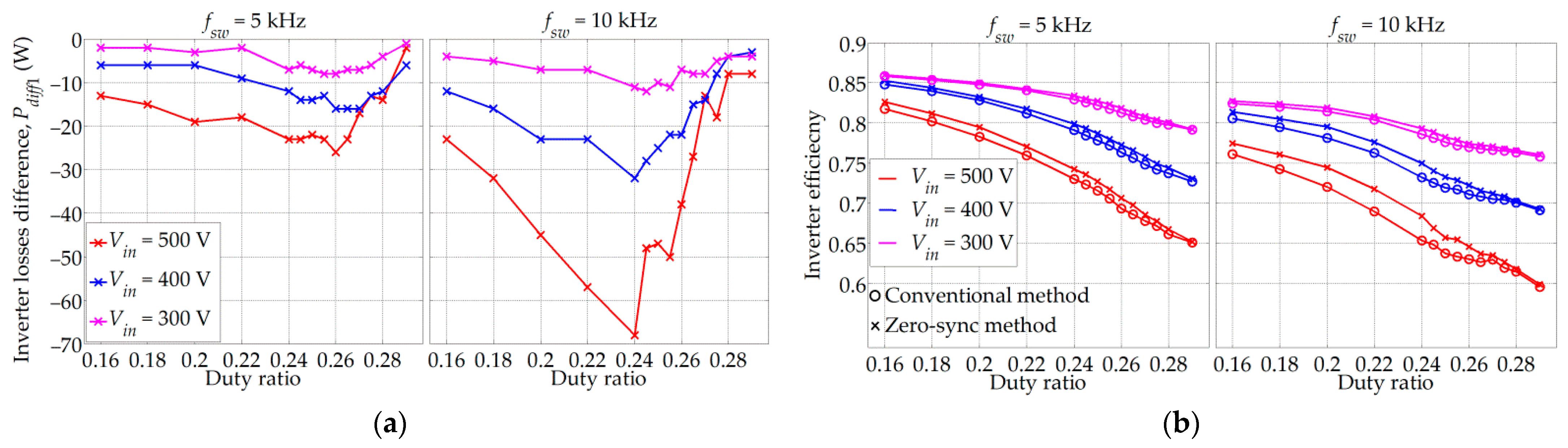
Figure 12 shows the inverter losses difference and the efficiency as a function of the duty ratio for different values of the load power and for the switching frequencies of 5 kHz and 10 kHz, with
Ma = 0.819 and
Vin = 500 V. The inverter losses difference (
Pdiff1) shown in
Figure 12a, obtained as
Pl−zsm–
Pl−cm, is negative for all the considered values of
D0, meaning that the inverter losses are lower in the case of the zero-sync method.
It is notable that
Pdiff1 varies with respect to the duty ratio. For example, for
fsw = 5 kHz, it may be noted that the absolute value of
Pdiff1 increases with
D0 in the range from 0.16 to about 0.26, and then it rapidly decreases. The described behavior of the inverter losses difference is related to the additional transistor switching occurring in the conventional STS injection method. The additional switching implies higher switching losses of the transistor. For
D0 ≤ 0.26, the duration of the additional ZSS is long enough to ensure both the mentioned switching transitions of the transistor to be finished completely. Hence, in this region, the switching losses of the transistors are dominant and increase with
D0 [
33] due to the increase of
Vpn as per (2). However, when the applied
D0 is higher than 0.26, the turn-on transition into the STS occurs before the previous turn-off transition from the active state into the ZSS has completely finished. This leads to a decrease of the corresponding switching losses, and consequently to a decrease of the
Pdiff1 absolute value. It is important to note that, in case
D0 =
D0,max is applied,
Pdiff1 is still negative, which confirms the claims stated in the last paragraph of
Section 3.
The similar behavior of
Pdiff1 with regard to the variation of
D0 was noted for
fsw = 10 kHz (right part of
Figure 12a). However, the absolute values of
Pdiff1 were in this case somewhat higher due to the increase of the switching transitions with
fsw and, hence, the increase of the switching losses. Note that the absolute value of
Pdiff1 increases with
D0 until the turning point (
D0 ≈ 0.24), which is in this case slightly lower compared to the previous example at
fsw = 5 kHz. This is related to the fact that the switching transitions occur more often at higher switching frequencies. However, since each transition of the transistor requires a certain amount of time to be executed, depending solely on its current and voltage, the inability of the transistor to completely turn-off from the active state into the ZSS occurs for lower values of
D0 compared to the example at
fsw = 5 kHz.
The variation of the load power did not have a clear impact on the inverter losses difference. This may be explained by the fact that the increase of the load power primarily leads to the increase of the transistor conduction losses, whereas the increase of the switching losses remains less pronounced [
33]. Note also that the load power of 3000 W was not achieved for
fsw = 10 kHz for both the considered methods because this would cause the case temperature of the IGBT-diode pair to surpass the maximum allowed temperature, set to 130 °C. This may ultimately destroy the device.
Figure 12b shows the inverter efficiency for the two considered STS injection methods. As expected, the inverter efficiency is higher in the case of the zero-sync method and it increases with the load power. The highest efficiency difference is noted for
D0 = 0.2 and
fsw = 10 kHz and amounts to approximately 4%. In addition, the inverter efficiency for both the considered methods decreases with
D0 increase due to the increase of
Vpn according to (2), which, in turn, implies higher switching losses. Moreover, lower efficiency is noted for the higher switching frequency, regardless of the applied STS injection method, which is again due to the higher switching losses.
Figure 13 shows the inverter losses difference and the efficiency as a function of the duty ratio for different values of the input voltage and the switching frequencies of 5 kHz and 10 kHz, with
Ma = 0.819 and
Pout = 1000 W. The variation of the inverter losses with respect to
D0 in
Figure 13a is practically the same as in
Figure 12a. However, the variation of the input voltage (
Vin) significantly affects the inverter losses difference. Note that by reducing the input voltage by 100 V, the absolute value of
Pdiff1 is about two times reduced. This is the consequence of
Vpn decreasing with
Vin according to (2), which in turn leads to the decrease of the switching losses. This effect is more pronounced at the higher switching frequency.
Figure 13b shows that the input voltage decrease favorably affects the inverter efficiency, primarily due to the decrease of the switching losses. The negative sign of
Pdiff1 for all the considered values of
D0 and
Vin implies that the zero-sync method ensures higher inverter efficiency compared to the conventional method. The smallest efficiency difference is observed for
Vin = 300 V and
fsw = 5 kHz and amounts to 0.5%, whereas the largest is observed for
Vin = 500 V and
fsw = 10 kHz and amounts to 2.5%.
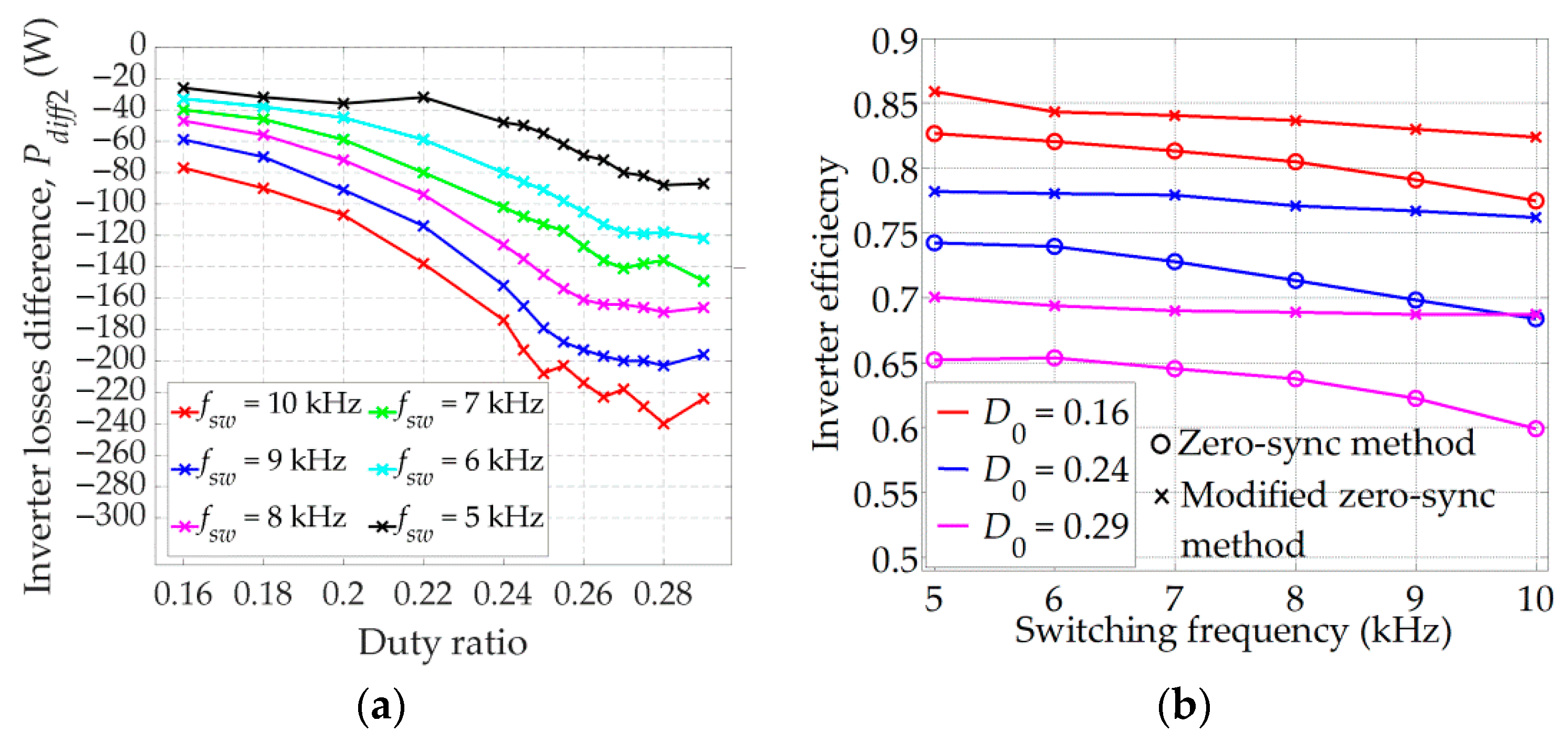
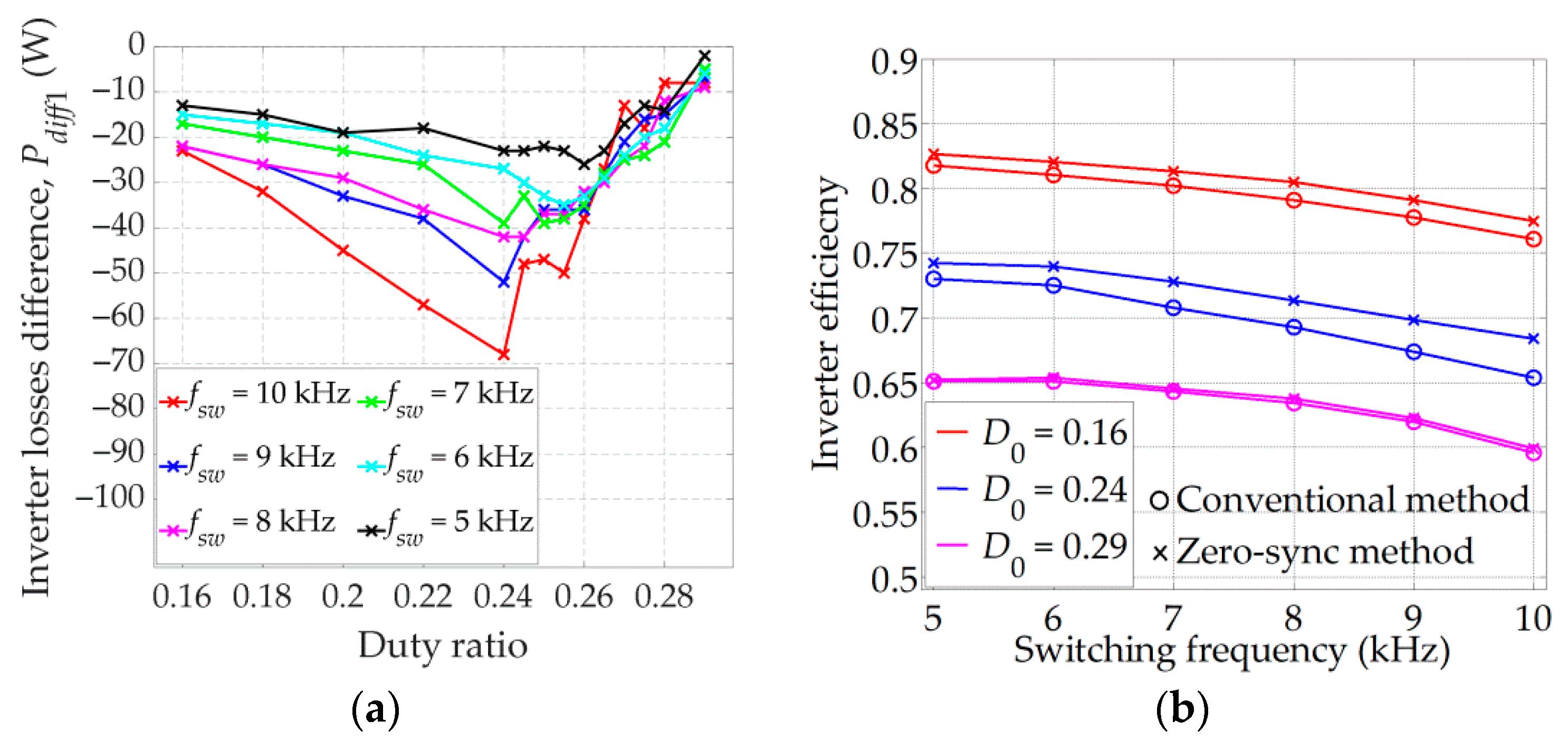
Figure 14a shows
Pdiff1 as a function of the duty ratio for different values of the switching frequency, with
Ma = 0.819,
Pout = 1000 W, and
Vin = 500 V. It may be concluded that the absolute value of
Pdiff1 increases with the switching frequency, which was expected due to the increased number of switching transitions, and hence the increased switching losses. Note that the turning point of
Pdiff1, after which the absolute value of
Pdiff1 starts to decrease with the increase of
D0, occurs for lower
D0 values as
fsw increases.
The inverter efficiency as function of the switching frequency, for the two considered STS injection methods, is shown in
Figure 14b. Three values of
D0 were considered–0.16, 0.24, and 0.29–with
Ma = 0.819,
Pout = 1000 W, and
Vin = 500 V. The inverter efficiency increases with the decrease of
D0 as well as with the decrease of
fsw, both due to the decrease of the switching losses. Note that the zero-sync method results in higher inverter efficiency for all the considered measurement points. The largest difference is noted for
D0 = 0.24 and
fsw = 10 kHz and amounts to 4%, whereas the smallest difference is noted for
D0 = 0.29 and
fsw = 5 kHz and amounts to 0.4%. This is in accordance with
Pdiff1 variation shown in
Figure 14a. The absolute value of
Pdiff1 for
D0 = 0.24 and
fsw = 10 kHz amounts to 70 W, whereas it amounts to only 3 W for
D0 = 0.29 and
fsw = 5 kHz.
6. Modified Zero-Sync Shoot-Through Injection Method with the Dead-Time
The experimental comparison of the zero-sync method and the conventional one proved the main advantage of the zero-sync method, which is the inverter efficiency increase. However, during the experimental investigation, differences were noted between the boost factor achieved through STS injection, defined in (1), and the actual boost determined as follows:
where
D0,act represent equivalent actual duty ratio calculated according to (2).
In the obtained results, the actual boost factor was always higher than the one achieved through the STS injection and this phenomenon was noted for both the considered STS injection methods. This was the result of unintended short circuiting across the inverter legs (i.e., unintended STSs) due to the non-ideal switching of the involved transistors. The dead-time prevents simultaneous conduction of the transistors in the same inverter leg by introducing the time delay into the PWM signals. So far, the dead-time was not implemented for the qZSI since it is not required due to the existence of the impedance network. However, this does not mean that the transistors in the same leg do not occasionally simultaneously conduct for a short amount of time during the non-STSs. This only means that this sporadic, unintended short circuiting can be tolerated within such a configuration. Hence, although this may not cause the qZSI failure, it results in higher-than-intended and uncontrollable qZSI voltage boost.
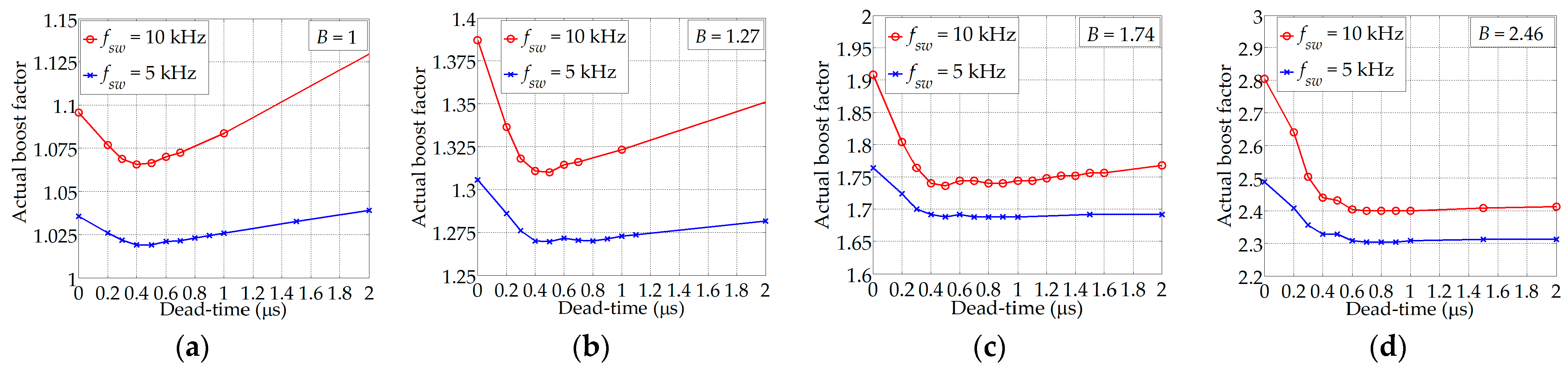
Figure 15 shows
Bact as a function of the introduced dead-time (τ
d) for different applied
B values and two switching frequencies, with
Vin = 500 V,
Pout = 1000 W, and
Ma = 0.819. The actual boost factor rapidly decreases with τ
d increase in the range 0 ≤ τ
d ≤ 0.7 μs for both the considered switching frequencies. This is because the duration of the additional, unintended short circuit occurrences is reduced by introducing the dead-time. Note that the actual boost is significantly higher in the case when the switching frequency is set to 10 kHz as compared to 5 kHz. This is because the higher
fsw implies lower
Tsw, so the time share of the additional short circuits within a single
Tsw increases. On the other hand, the increase of the actual boost factor with the dead-time is noted for τ
d > 0.7 μs for both the considered switching frequencies. This is related to the blocking of the impedance network diode during the non-STSs, which is caused by the dead-time injection. The increase of τ
d implies the decrease of the output voltage and the load power, which, in turn, results with the decrease of the qZSI input current. Therefore, the non-STSs are bound to last longer than the inductor discharging time, causing
D1 to block the current, thus increasing the boost factor [
34,
35]. Finally, it was decided to introduce the dead-time into the SPWM of the considered qZSI with the optimal value of τ
d selected to be 0.7 μs. This value is high enough to prevent the occurrence of the additional short circuit occurrences during the SPWM switching transitions, whereas the higher values of τ
d would cause the blocking of
D1 and higher distortion of the inverter output voltage.
The modified zero-sync method of STS injection is practically the zero-sync method with the introduced dead-time of optimal duration.
Figure 16a shows the characteristic waveforms of the zero-sync method. The dead-time, depicted by the yellow areas in
Figure 16, is injected into the transistor pulses to postpone the turn-on transition into the active SPWM state. This prevents the short circuiting of the corresponding inverter leg during the SPWM switching transitions. However, it may also disrupt the detection of the ZSSs. This can be described by considering the waveforms of the SPWM with introduced dead-time, but with omitted STSs, which are shown in
Figure 16b. There are two ZSSs within a single
Tsw, as is shown in the rectangle in
Figure 16b. During the first ZSS, the switching pulses
SA+,
SB+, and
SC+ are equal to 0, whereas
SA−,
SB−, and
SC− are equal to 1. However, during the second ZSS, the opposite holds. The first ZSS occurs when the
SA+ value becomes 0, whereas the second ZSS occurs when the
SB− value becomes 0. Thus, the occurrence of the ZSS is in the first case determined by the upper transistor switching pulse and by the lower transistor switching pulse in the second case. The same may be noted within each
Tsw. That practically means that the first ZSS has to be detected when the switching pulses
SA+,
SB+, and
SC+ are equal to 0, whereas the second ZSS has to be detected when the switching pulses
SA−,
SB−, and
SC− are equal to 0. Therefore, the switching pulses of all the transistors needed to be utilized for the detection of the ZSS for the hardware implementation of the modified zero-sync method.
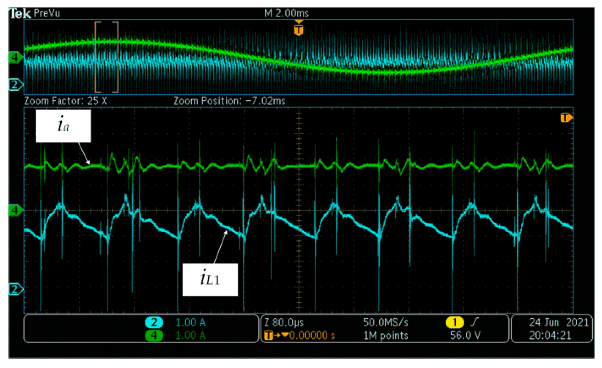
Figure 17 shows the waveforms of the load phase current in the phase A (
ia) and the qZSI input current (
iL1) in the case of implementing the zero-sync method with dead-time. The measurements were carried out with
fsw = 5 kHz,
D0 = 0.24,
Ma = 0.819,
vin = 500 V, and the load power set to 1000 W. The output phase current is practically sinusoidal with the THD of 1.9%. Moreover, by the comparison of the
iL1 waveforms shown in
Figure 10 and
Figure 17, it may be concluded that there is no notable difference in the ripple of the inductor current between all the three methods considered in this paper, namely the zero-sync method with and without dead-time and the conventional method.
The evaluation of the zero-sync method with dead-time is provided through the comparison to the zero-sync method without dead-time. The main comparison parameters were the same as those used in
Section 5: the power losses difference (
Pdiff2) and the inverter efficiency difference. The inverter losses in the case of the modified zero-sync method (
Pl−mzsm) were calculated as
Pin−mzsm −
Pout−mzsm, whereas
Pdiff2 was calculated as
Pl−mzsm −
Pl−zsm.
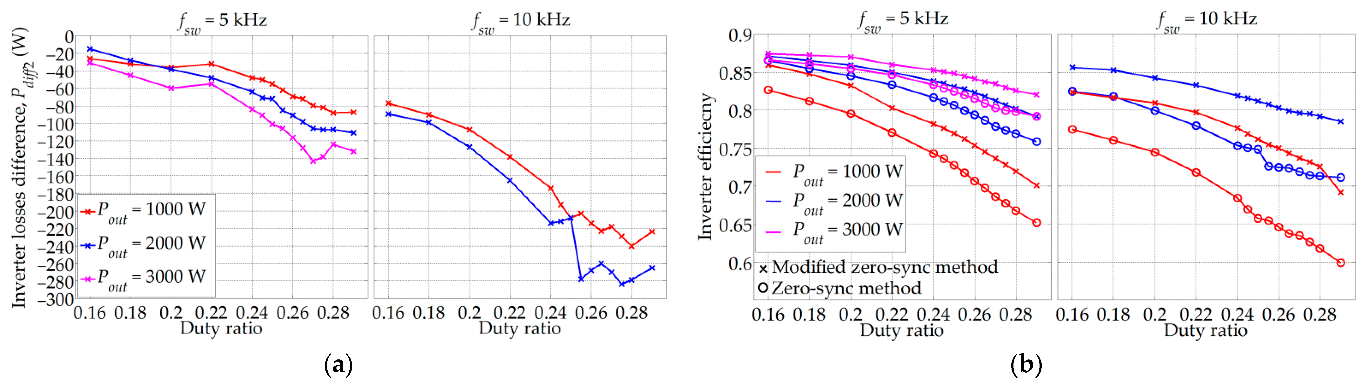
Figure 18 shows
Pdiff2 and the inverter efficiency as a function of the duty ratio for different load power values and the switching frequencies of 5 kHz and 10 kHz, with
Ma = 0.819 and
Vin = 500 V. The inverter losses are significantly reduced by introducing the dead-time, whereas the absolute value of
Pdiff2 increases with the load power. The largest absolute value of
Pdiff2, noted for
fsw = 10 kHz,
D0 = 0.28, and
Pout = 2000 W, amounts to 280 W, which results in the inverter efficiency increase of 11%. The lowest absolute value of
Pdiff2, noted for
fsw = 5 kHz,
D0 = 0.16, and
Pout = 2000 W, amounts to 18 W, which results in the inverter efficiency increase less than 1%.
Figure 19 shows
Pdiff2 and the inverter efficiency as a function of the duty ratio for different input voltage values and the switching frequencies of 5 kHz and 10 kHz, with
Ma = 0.819 and
Pout = 1000 W. Note that by reducing the input voltage by 100 V, the absolute value of
Pdiff2 is reduced by a factor of two. Likewise, by decreasing the switching frequency from 10 kHz to 5 kHz, the absolute value of
Pdiff2 is again reduced by a factor of two. Therefore, the largest
Pdiff2 absolute value of 240 W is noted for
fsw = 10 kHz and
Vin = 500 V (efficiency boost of 10%), whereas the lowest
Pdiff2 absolute value of 10 W is noted for
fsw = 5 kHz and
Vin = 300 V (efficiency increase less than 1%).
Figure 20a shows
Pdiff2 as a function of the duty ratio for different values of the switching frequency, with
Ma = 0.819,
Pout = 1000 W, and
Vin = 500 V. For the same utilized value of the STS duty ratio, the absolute value of
Pdiff2 increases with the switching frequency due to the increase of the switching losses. It is interesting to observe how the mentioned fact affects the inverter efficiency.
Figure 20b shows the inverter efficiency as a function of the switching frequency for three values of
D0, namely 0.16, 0.24, and 0.29, with
Ma = 0.819,
Pout = 1000 W, and
Vin = 500 V. As expected, the inverter efficiency is higher when the dead-time is implemented, with the difference between the two considered methods increasing with
D0. The decrease of the inverter efficiency with the
fsw increase noted in the case of the modified zero-sync method is lower compared to the non-modified zero-sync method.
The inverter losses differences that occur with regard to different STS injection methods should be reflected in different case temperatures of the utilized IGBT-diode pairs. Therefore, the case temperature of the IGBT-diode pairs was measured in steady state by means of the thermal camera Testo 865 (Testo).
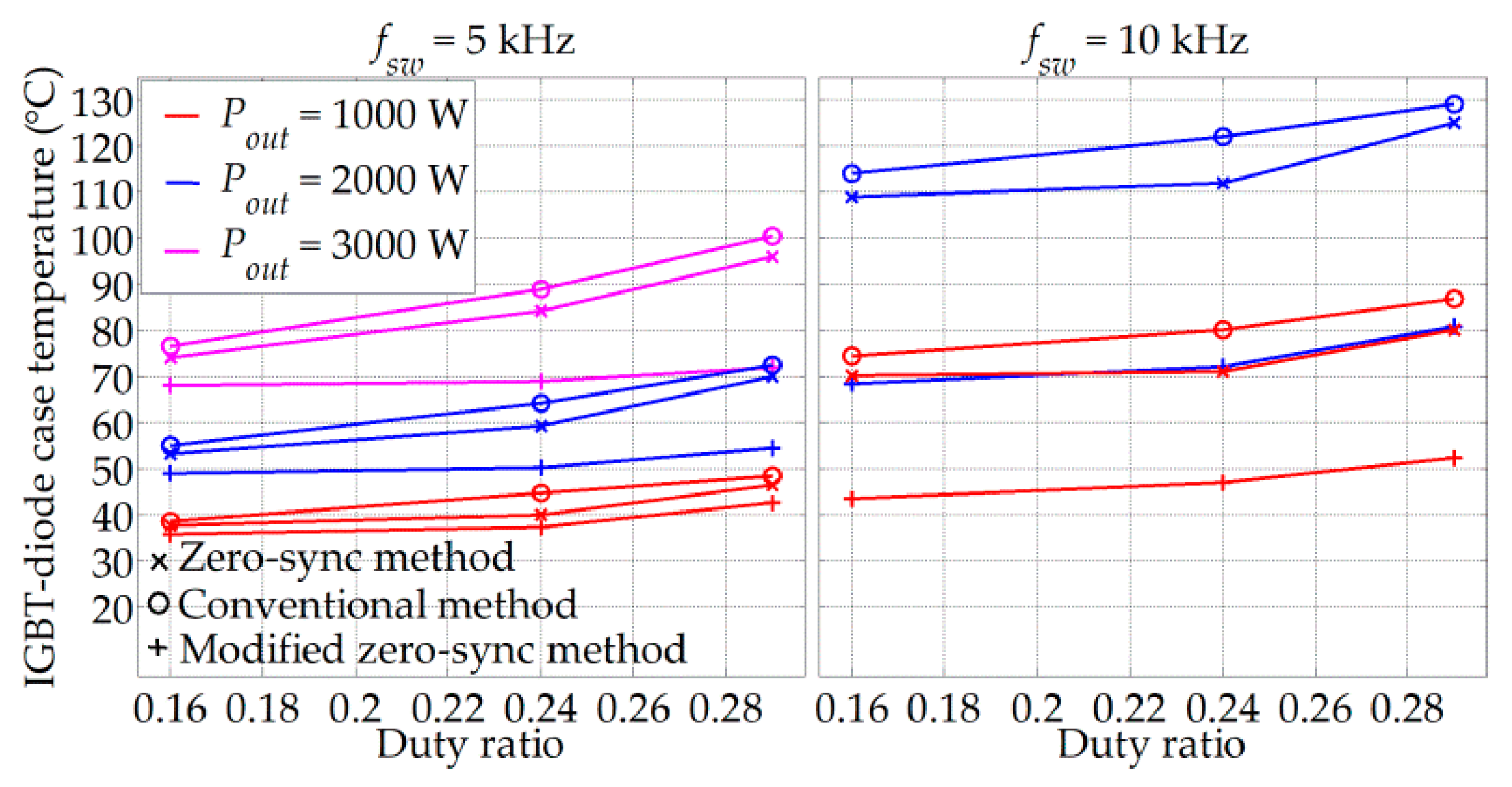
Figure 21 shows the case temperature with respect to the duty ratio for all three STS injection methods considered in this study. Three values of
D0 and three values of the load power were considered for the switching frequencies of 5 kHz and 10 kHz. The highest case temperatures were noted for the conventional method, the zero-sync method resulted with medium temperature values, whereas the implementation of the modified zero-sync method resulted with convincingly the lowest case temperatures. For example, for
fsw = 10 kHz,
Pout = 2000 W, and
D0 = 0.29, the case temperature difference between the modified zero-sync method and the other two methods amounts to approximately 50 °C. Consequently, the implementation of the modified zero-sync method results in an increase of the inverter power rating since the inverter losses and the case temperatures are in this case reduced.


