Article

In Situ Recrystallization of Co-Evaporated Cu(In,Ga)Se2 Thin Films by Copper Chloride Vapor Treatment towards Solar Cell Applications

1
Virginia Institute of Photovoltaics, Old Dominion University, Norfolk, VA 23529, USA
2
Department of Metallurgical and Materials Engineering, Colorado School of Mines, Golden, CO 80401, USA
3
Institut des Materiaux Jean Rouxel, Universite de Nantes, 44322 Nantes, France
*
Author to whom correspondence should be addressed.
Energies 2021, 14(13), 3938; https://doi.org/10.3390/en14133938
Submission received: 25 May 2021 / Revised: 25 June 2021 / Accepted: 28 June 2021 / Published: 1 July 2021
(This article belongs to the Special Issue Advances in Devices for Energy Generation and Storage)

Abstract

:
Cu(In,Ga)Se2 (or CIGS) thin films and devices were fabricated using a modified three-stage process. Using high deposition rates and a low temperature during the process, a copper chloride vapor treatment was introduced in between the second and third stages to enhance the films properties. X-ray diffraction and scanning electron microscopy demonstrate that drastic changes occur after this recrystallization process, yielding films with much larger grains. Secondary ion mass spectrometry shows that the depth profile of many elements is not modified (such as Cu, In and Se) while others change dramatically (such as Ga and Na). Because of the competing effects of these changes, not all parameters of the solar cells are enhanced, yielding an increase of 15% in the device efficiency at the most.

Graphical Abstract

1. Introduction

High quality copper indium gallium diselenide (Cu(In,Ga)Se2 or CIGS) semiconductors for application in thin film solar cells are often obtained by complex fabrication processes [1,2]. CIGS materials, engineered via the so-called three-stage co-evaporation process, transform basic materials into devices with power conversion efficiency above 23% under AM1.5G illumination [3]. This process uses substrates temperature as high as 550 °C, and does not yet yield competitive prices with technology, such as crystalline silicon. Advancements in the area of processing, with a focus on best possible economic viability, are centered on simultaneously increasing the deposition rate while reducing the deposition temperature, all of this while maintaining a high efficiency [4]. An example of such a high speed and low temperature industrial process can be found in CdTe solar cells, where CdCl2 annealing process is used in conjunction with small quantity oxygen at 415 °C [5]. This specific process results in the recrystallization of CdTe and enhanced solar cell performance. Even though certain conventional procedures, such as annealing under hydrogen selenide gases or annealing treatments in selenium, have been used to recrystallize CIGS, optimal results have not been achieved so far [6,7,8].
In this paper, we investigated the influence of deposition parameters on the in situ recrystallization, under CuCl2 vapor, of CIGS thin films deposited by three-stage co-evaporation process at high deposition rates and low temperatures. Thin films and devices characterizations were performed and the results were analyzed as a function of the deposition parameters.

2. Experimental Methods

A molybdenum (2.00″ diameter × 0.250″ thick, purity-99.95%, Kurt J. Lesker, Pittsburgh, USA) bilayer was first deposited by dc magnetron sputtering (PVD 75, Kurt J. Lesker) on soda-lime glass (SLG) substrates at constant power density of 7.4 W/cm2, resulting in a thickness of about 800 nm. CIGS absorber layers were then fabricated following a three-stage co-evaporation (Kurt J. Lesker) process with high deposition rates (around 10 μm/hr), with low substrate temperatures for the second and third stages. First, In, Ga and Se were co-evaporated (third stage), followed by the co-evaporation of Cu and Se (second stage). During the third stage, In, Ga and Se were again co-evaporated until the films became Cu-poor ([Cu]/([In] + [Ga]) < 1), as detected by a mass spectrometer [9,10]. The in situ recrystallization process was conducted in between the second and the third stages by flashing 20 mg of CuCl2 (Alfa Aesar) for 1 min. No additional post-deposition treatment, such as evaporating sodium fluoride or potassium fluoride [11,12], was performed. Some samples were produced separately for reference without CuCl2 evaporation and are referred to as “Reference” samples in the text.
The main parameter changed for this set of experiments was the substrate temperature (TSS) for the second and third stages, as shown in Table 1. The results will, therefore, be presented as a function of second stage temperature dependence and third stage temperature dependence.
Devices were fabricated using these various processes. The CIGS devices were fabricated with a typical SLG/Mo/CIGS/CdS/i-ZnO/ITO/grids structure with SLG as a substrate, Mo as a back contact, CIGS as an absorber layer, CdS as a buffer layer and i-ZnO/ITO as transparent conducting oxides. CIGS absorber layers were deposited using one of the five processes mentioned in Table 1. The junction was formed with CIGS layer by depositing an 80 nm CdS layer using chemical bath deposition. Afterward, a transparent conducting oxide bilayer consisting of i-ZnO/ITO (2.00″ diameter × 0.250″ thick, purity-99.99%, Kurt J. Lesker, Pittsburgh, USA) (80 nm/250 nm) was deposited by r.f. sputtering (PVD 75, Kurt J. Lesker). The metal contacts were deposited by e-beam (PVD 75, Kurt J. Lesker, Pittsburgh, USA), followed by mechanical scribing to define solar cells with active area of 0.5 cm2. The photovoltaic characteristics of the devices were then evaluated by current density-voltage (J-V) measurements (IV5, PV Measurements Inc., Boulder, USA) under AM 1.5G with light intensity of 100 mW/cm2 at 25 °C and by external quantum efficiency (EQE) measurements (QEX7, PV Measurements Inc., Boulder, USA).
The thickness of each film was measured using a thickness profilometer (DektakXT Profilometer, Bruker, Tucson, AZ, USA). The films composition was measured by X-ray fluorescence (XRF) (Solar Metrology, Saugerties, NY, USA, System SMX). Surface and cross-section morphological analyses were performed by scanning electron microscopy (SEM) (JEOL JSM-6060LV). The crystallographic structure analysis was done by symmetric θ-2θ X-ray diffraction (XRD) (Miniflex II Benchtop Diffractometer, Rigaku, Tokyo, Japan). The elemental composition profile of the films was measured by dynamic secondary ion mass spectrometry (SIMS) using an ION-TOF SIMS V instrument.

3. Results and Discussions

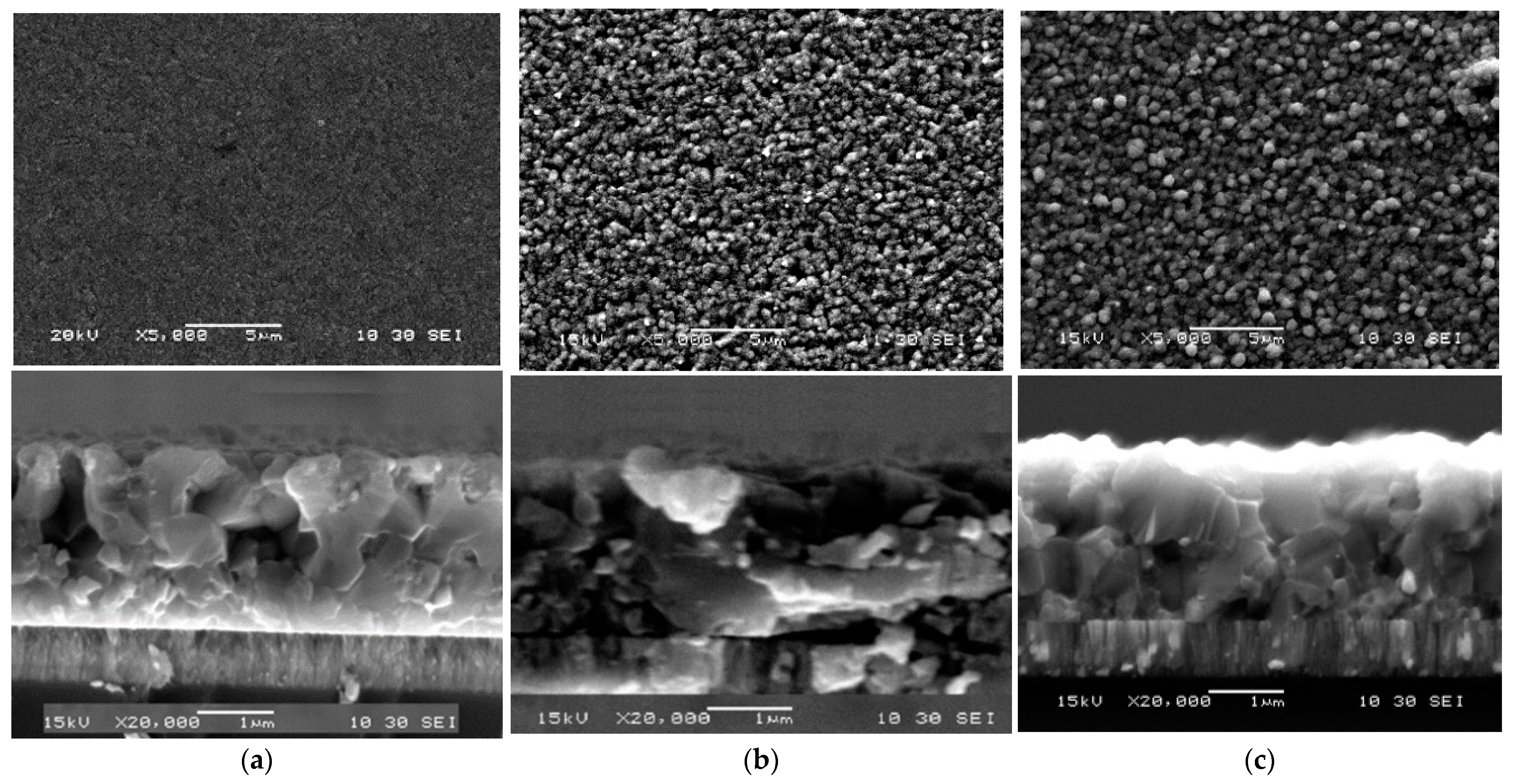
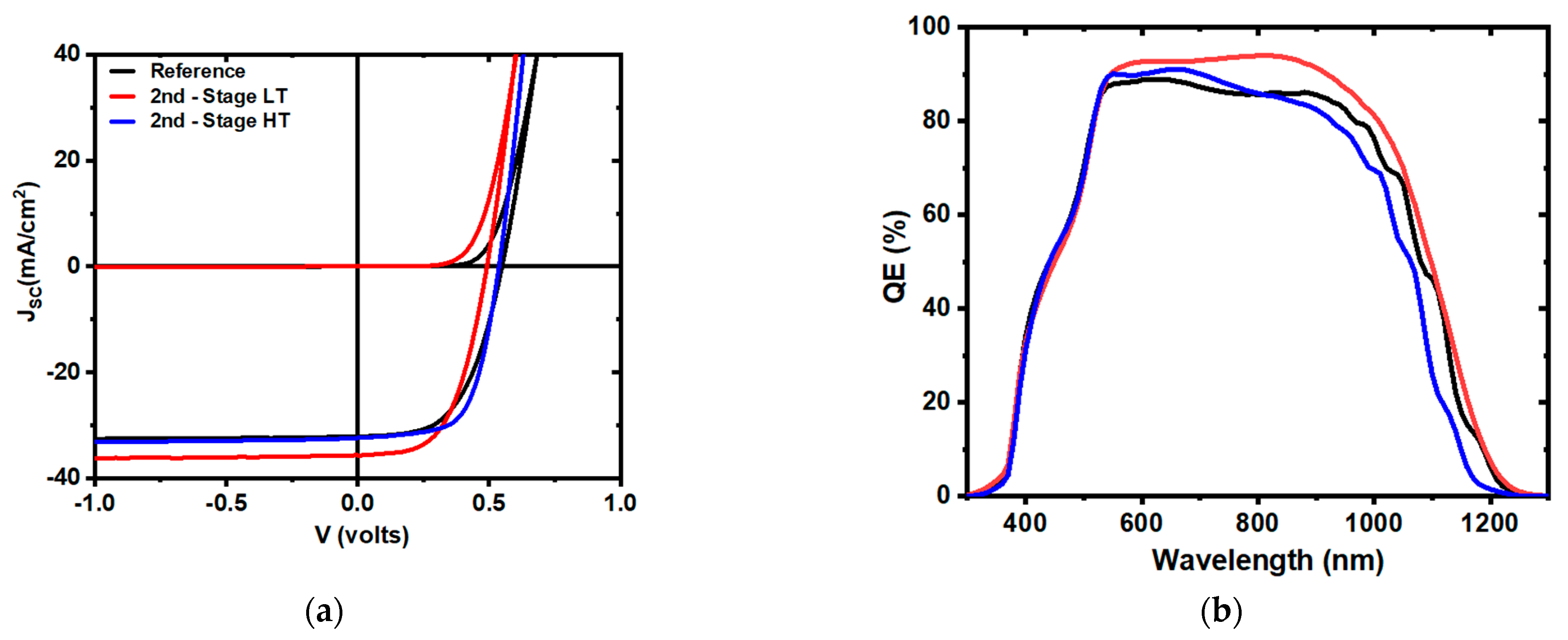
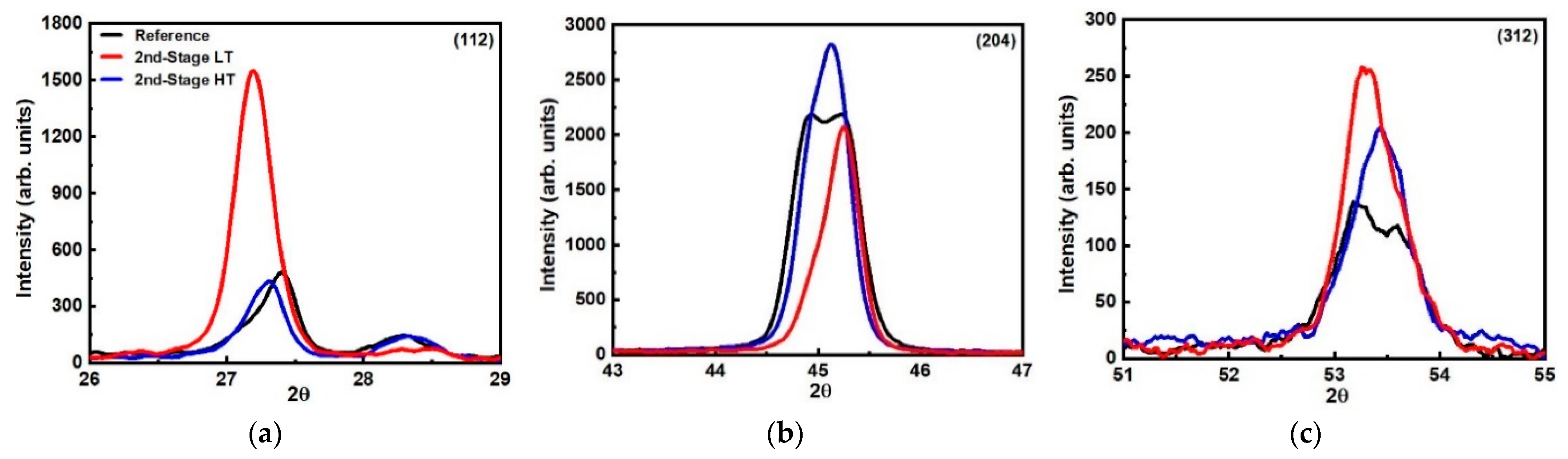
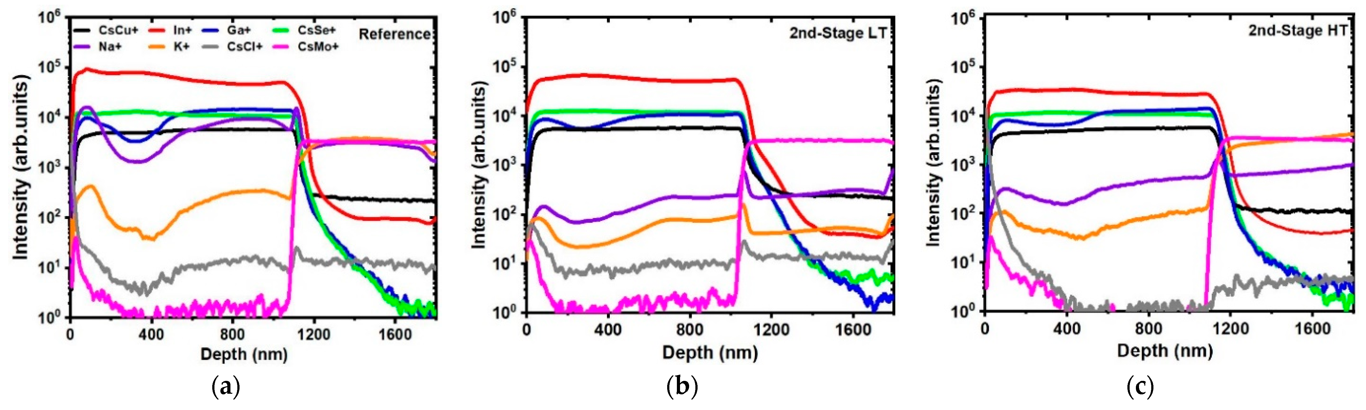
3.1. Second Stage Temperature Dependence

As mentioned previously, two different sets of runs were completed with two distinct substrates temperature for the second stage, nominally at 350 °C (second stage LT) and 400 °C (second stage HT). For the first and third stages, the temperatures were kept constant at 350 °C and 400 °C, respectively. The samples were recrystallized by flashing 20 mg of CuCl2 in 1 min in between the second stage and the third stage, once the substrates temperature reached 400 °C. Reference samples were also fabricated separately. The modification of the surface and cross-section morphology of these films before and after recrystallization was observed by SEM as shown in Figure 1. A clear change in grain size as the thin film develop from small grains to large grains after recrystallization at both specific temperatures. As compared to 350 °C, samples recrystallized at 400 °C seemed to have more compact, distinct and uniform grain sizes.
XRD measurements were performed on the reference and recrystallized films in order to assess how the structure of the film changed with treatment (Figure 2). The parameters extracted from the measurements are presented in Table 2. There is a clear change for the (112) peak, with a much higher intensity for the 350 °C samples, whereas the 400 °C samples tend to have a slightly higher intensity for the (220)/(204) peak, indicating a different preferential orientation for both films. Overall, there is a decrease in the full width at half maximum (FWHM) and an overall increase in peak integrated intensity for both recrystallized films, indicating an increase in the films’ crystallinity. The other notable change is a shift in peak position, more pronounced for the second stage LT. However, one can notice that the (112) peak shifts towards lower angle (indicating a lower gallium content), while the (220)/(204) peak shifts toward higher angle. Overall, this would seem to indicate a redistribution of gallium rather than a change of film composition. This was confirmed by XRF measurements (Table 2), with the Cu/III and Ga/III ratio barely changing from one film to another.
The samples were also investigated by SIMS depth profile, with the matrix element of each layer being characterized. SIMS was used notably to determine whether there was a redistribution of gallium within the films and further helps to understand the recrystallization process. The depth profiles for the positive ions of the main elements are shown in Figure 3. In the reference samples, the constant ion profiles for CIGS main elements (Cu, In and Se) and the presence of alkali are consistent with CIGS films deposited by a three-stage process [13]. No change was observed for the Cu, In or Se profiles before and after annealing. No significant signal is observed for chlorine even after recrystallization, which seems to indicate that the element does not remain in the films despite enhancing the grains. As shown by SIMS, the reference sample has a deep Ga notch, typical of CIGS films deposited by a three-stage process [14]. As CuCl2 is introduced, the depth of the notch decreases significantly and nearly disappear for the second stage HT, indicating the interdiffusion of Ga due to the treatment. This is consistent with the observation by XRD. Looking at the sodium profile, the overall Na intensity decreased after recrystallization compared to the reference sample. This might suggest that the change in grain boundaries density, due to the increase of grain size, reduces the possible path for sodium to diffuse through the films [15].
Figure 4 shows the J-V and QE plots for the CIGS solar cell devices fabricated using the previous second stage processes. Table 3 lists the solar cell parameters extracted from the analysis shown in Figure 4. A single diode model using the dark I-V curves was used to extract the diode parameters. It can be seen that there is a modification of all the parameters with recrystallization. The second stage LT has a higher short circuit current density but lower open circuit voltage, despite having the same band gap as the reference sample, as can be seen from the QE. The fill factor is nearly the same for both samples, with similar values for the series and the shunt resistances. For the second stage HT, the open circuit voltage and the short circuit current density are similar to the reference samples, but there is an increase in the fill factor, from 54.8% to 63.3%, leading to an increase of efficiency from 9.6% to 11.0%. It is interesting to see that the shunt resistance is slightly higher while the series resistance is lower. Furthermore, the diode quality factor decreases from 1.8 to 1.6, while the reverse saturation current density decreases down to 2.0 × 10⁻⁸ mA/cm2. The band gap for the second stage HT seems to be higher than for the reference sample. This can be associated with the modification of the gallium profile after recrystallization, as seen by SIMS, whereby the second stage HT had a nearly flat profile for the gallium, losing the low band gap at the notch.

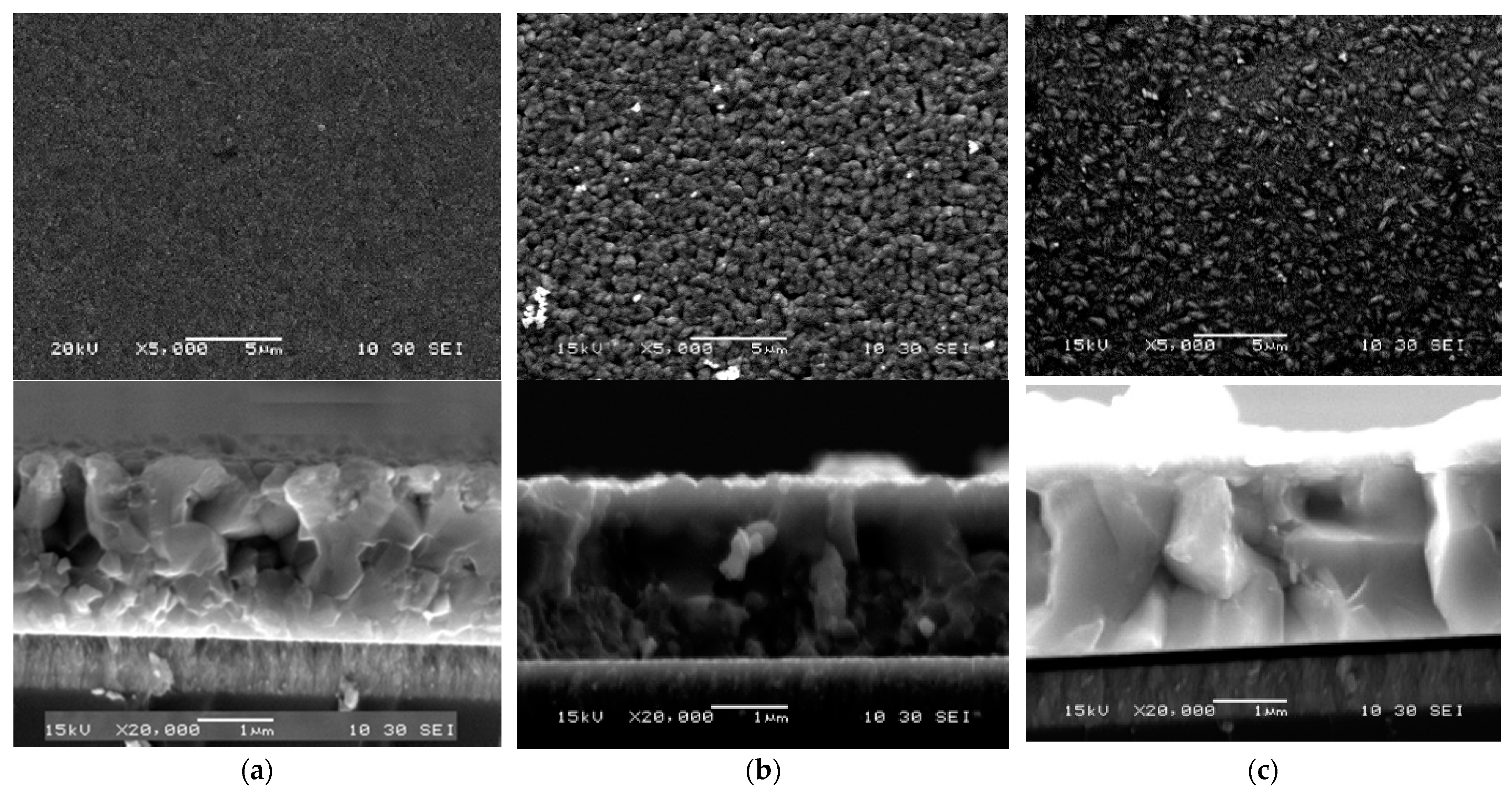
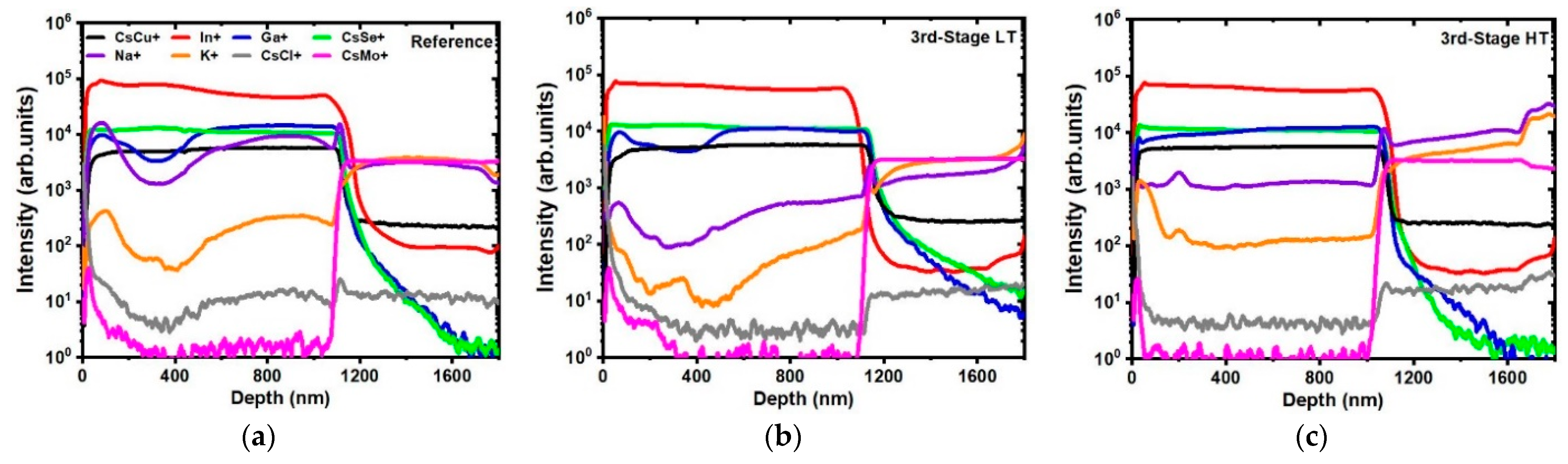
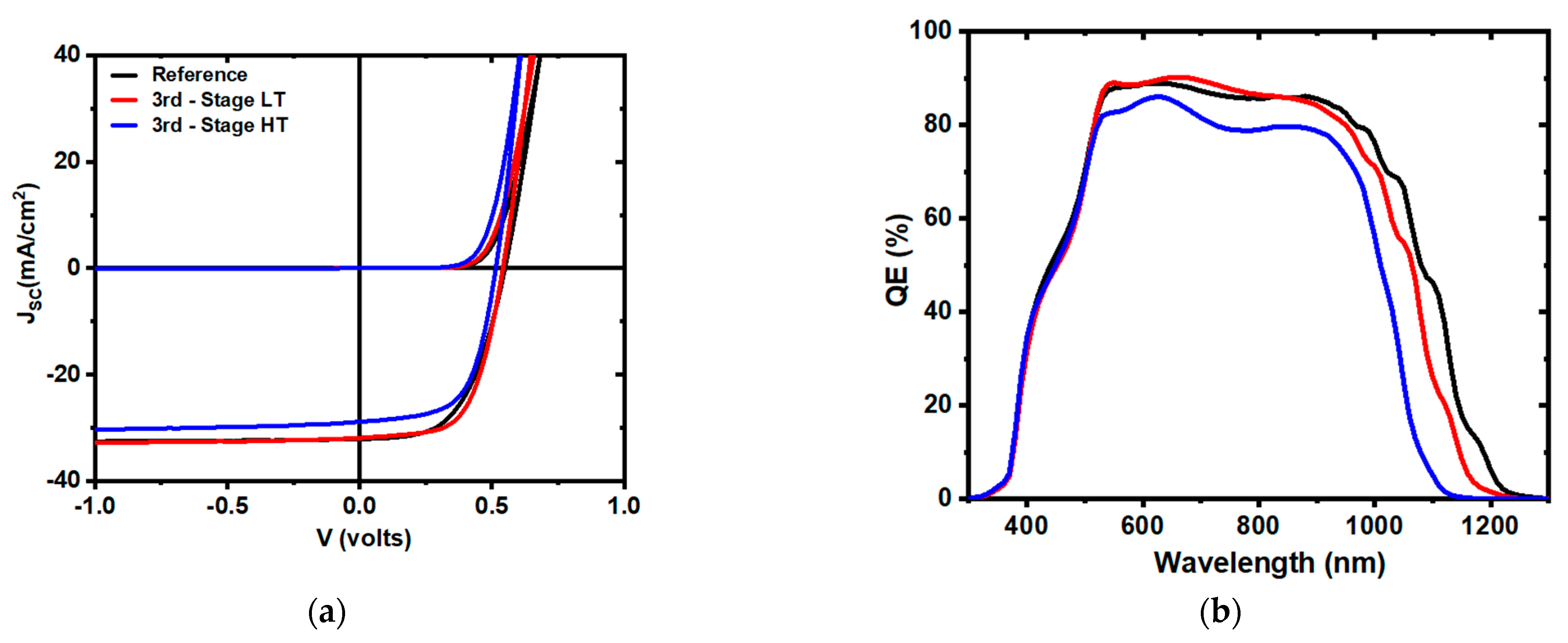
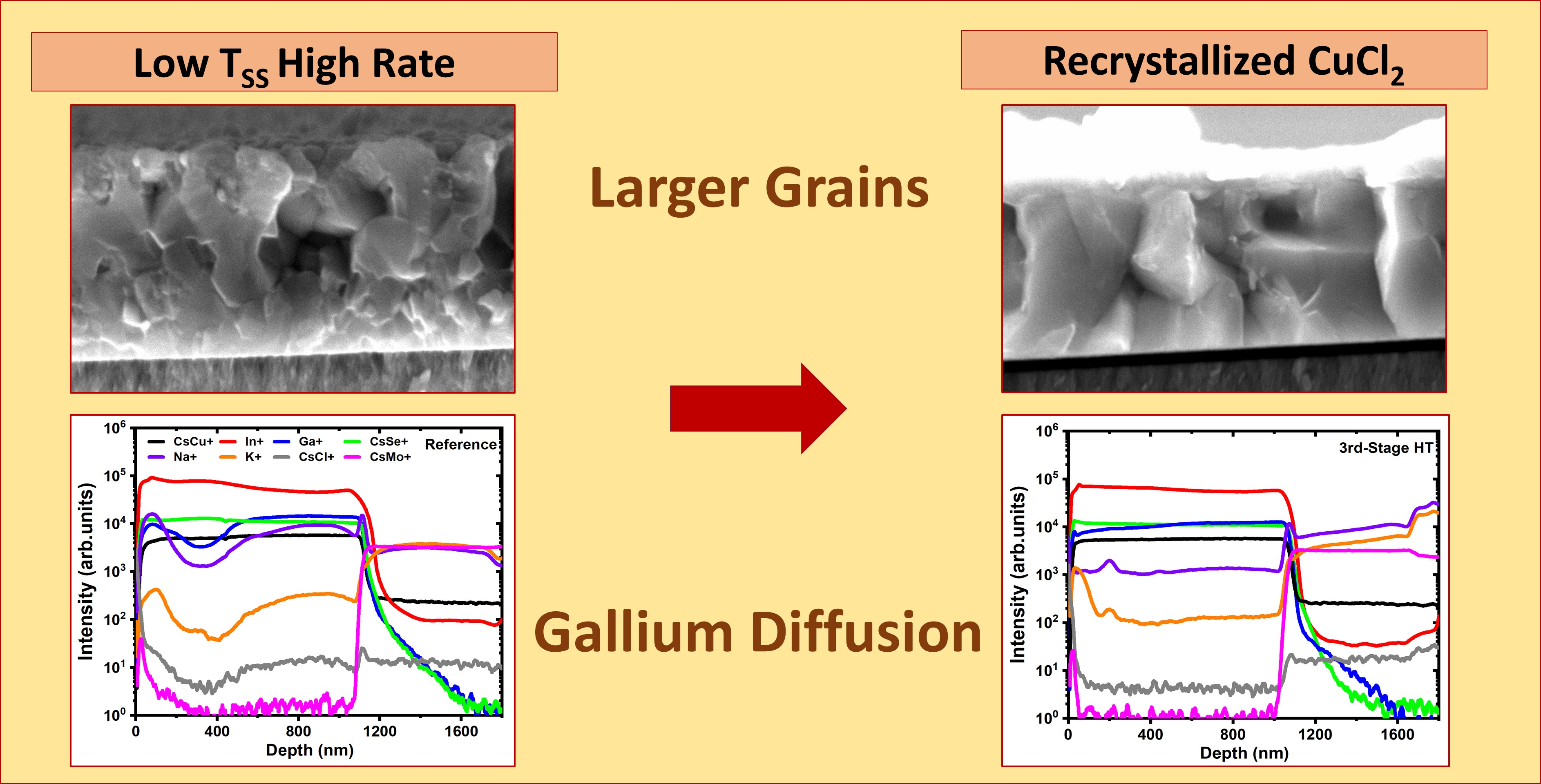
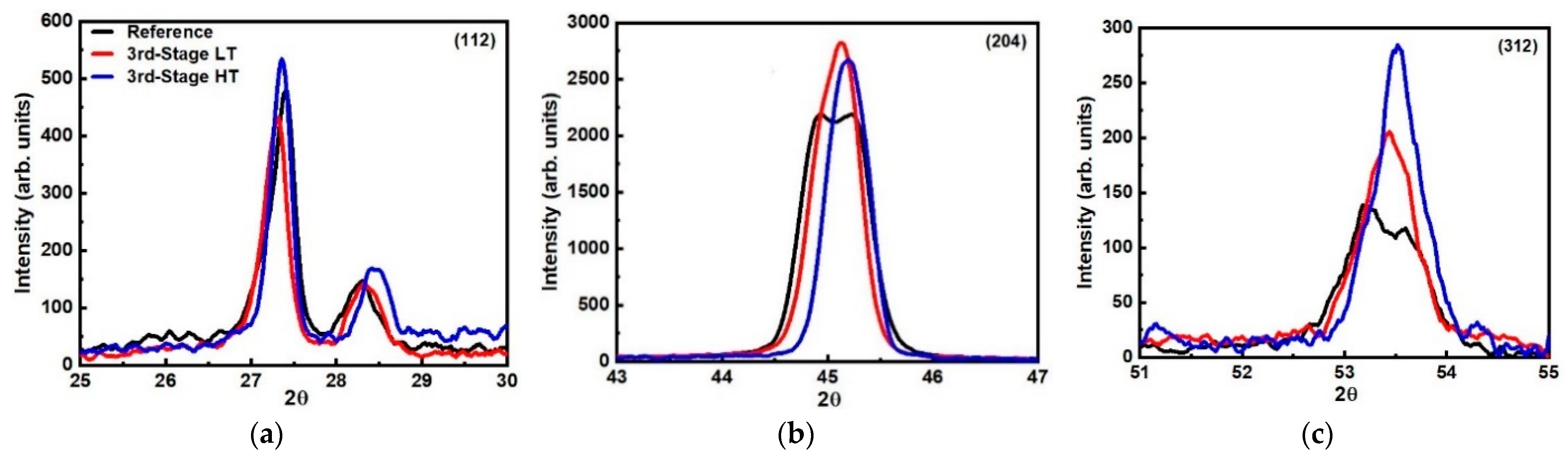
3.2. Third Stage Temperature Dependence

Another set of runs was done, whereby the third stage temperature was modified to either 425 °C (third stage LT) or 450 °C (third stage HT). For the first and second stages, the temperature was kept constant at 350 °C and 400 °C, respectively (see Table 1). The CuCl2 treatment was similar to the one used previously, with 20 mg of CuCl2 flashed in 1 minute in between the second stage and the third stage. Surface and cross-section morphology were analyzed by SEM and revealed an increase in grain dimension as compared to the reference samples (Figure 5). The samples recrystallized at 425 °C illustrates a slight change in the microstructure, whereas for the films recrystallized at 450 °C, the images show a considerable microstructural evolution. The films have larger grains with a size equal or close to the entire thickness. Comparing the SEM for the second stage HT and the third stage HT (Figure 1c and Figure 5c), one can see that the higher temperature during the third stage (450 °C versus 400 °C) clearly helps in enhancing the uniformity and the size of the grain, as expected.
XRD measurements were performed to better understand how the crystallinity of the films changed with recrystallization (Figure 6). The corresponding parameters are shown in Table 4. Few changes are observed for the (112) peaks regardless of the process, even though there is a small decrease in the FWHM as the temperature is increased. For the (220)/(204) peaks, one can see that the peak intensity increases and the FWHM decreases with an increase in the temperature, but also that the two peaks that could be observed for the reference sample are convoluted for the third stage LT, indicating a change in the composition or a redistribution of the gallium throughout the films. Composition measurements by XRF indicate that the overall film composition is not changing, which seem to indicate, therefore, a modification of the gallium profile.
To further elucidate the compositional profile, SIMS measurements were performed (Figure 7). Similarly to the second stage process modification, no clear change in the Cu, In and Se profiles can be seen, but a drastic change in the Ga profile is observed. Effectively, the Ga notch disappears for the third stage HT and a nearly flat Ga profile remains. Similarly, the sodium profile is modified, and the nearly flat sodium profile remains for the third stage HT, with an overall decrease of intensity for this element in the CIGS, but an increase in the Mo layer.
Figure 8 shows the J-V and QE plots for the CIGS solar cell devices fabricated using the previous third stage processes. Table 5 lists the solar cell parameters extracted from Figure 8 analysis. It can be seen that there is a modification of most of the parameters with recrystallization, with a clear enhancement of the fill factor and diode quality factor. One can see that there is a decrease in the short circuit current density for the third stage LT, which corresponds to a higher band gap according to the QE. This is in good agreement with the flatter Ga profile seen by SIMS, whereby the low band gap, which normally occurs due to the Ga notch in conventional three-stage processes, and which can be seen for example in the reference sample, does no longer exist in the third stage HT. This factor, along with a lower sodium concentration, probably also resulted in a lower open circuit voltage, despite a much larger grain than for the reference sample. The enhanced fill factor for the recrystallized samples seems to originate from slightly better shunt resistance, series resistance and diode quality factor. It is interesting to note that there is some voltage-dependent current collection for the third stage HT samples, indicating shorter diffusion length for the minority carriers potentially associated with the modified gallium profile.

4. Conclusions

Cu(In,Ga)Se2 (or CIGS) thin films and solar cells were fabricated using a modified three-stage process, at low temperature and high deposition rates, by modifying both the temperature of the second stage and the third stage, and evaporating CuCl2 in between these last two stages. Dramatic changes in morphology and crystallographic structures were observed by XRD and SEM, while SIMS confirmed a modification of some elements’ depth profiles, notably gallium and sodium. Interestingly, the overall composition of the films did not change with the recrystallization process. Because of the low temperature and high deposition rates used, the devices fabricated did not reach as high efficiency as we would normally get [16,17], but interesting trends could be seen. As is usual with CIGS solar cells, and with many other devices, competing properties can yield better or worse efficiency. In our case, larger and more uniform grain sizes were obtained with the recrystallization process, with no modification of the depth profiles for most elements. Unfortunately, both gallium and sodium were modified in a direction that does not seem beneficial, as the device efficiency only increased by 15% (1.4% absolute). The problem of the sodium can easily be solved by post deposition treatments, and potentially even double post deposition treatment with both sodium and potassium [18]. The loss of the gallium profile could be potentially be corrected by depositing pre-emptively a different gallium profile to take into account the redistribution. Both modifications should yield better devices even at these low temperatures and high rates, by taking advantage of this modified deposition process.

Author Contributions

Conceptualization, S.M. and A.R.; methodology, S.M., D.P., and T.A.; validation, D.P., G.R., E.P., T.L., B.B. and S.K.; formal analysis, D.P. and B.B.; resources, A.R. and S.M.; writing—original draft preparation, S.M., D.P. and B.B.; writing—review and editing, A.R., T.A., G.R., E.P., T.L. and S.K.; supervision, A.R. and S.M.; funding acquisition, S.M. and A.R. All authors have read and agreed to the published version of the manuscript.

Funding

This research was funded by the U.S. Department of Energy, grant number DE-EE0007551.

Conflicts of Interest

The authors declare no conflict of interest.

References

  1. Kaelin, M.; Rudmann, D.; Tiwari, A.N. Low cost processing of CIGS thin film solar cells. Sol. Energy 2004, 77, 749–756. [Google Scholar] [CrossRef]
  2. Niki, S.; Contreras, M.; Repins, I.; Powalla, M.; Kushiya, K.; Ishizuka, S.; Matsubara, K. CIGS absorbers and processes. Prog. Photovolt. Res. Appl. 2010, 18, 453–466. [Google Scholar] [CrossRef]
  3. Green, M.A.; Dunlop, E.D.; Hohl-Ebinger, J.; Yoshita, M.; Kopidakis, N.; Hao, X. Solar cell efficiency tables (version 56). Prog. Photovolt. Res. Appl. 2020, 28, 629–638. [Google Scholar] [CrossRef]
  4. Wang, H.; Zhang, Y.; Kou, X.L.; Cai, Y.A.; Liu, W.; Yu, T.; Pang, J.B.; Li, C.J.; Sun, Y. Effect of substrate temperature on the structural and electrical properties of CIGS films based on the one-stage co-evaporation process. Semicond. Sci. Technol. 2010, 25, 055007. [Google Scholar] [CrossRef]
  5. McCandless, B.E.; Moulton, L.V.; Birkmire, R.W. Recrystallization and sulfur diffusion in CdCl2-treated CdTe/CdS thin films. Prog. Photovolt. Res. Appl. 1997, 5, 249–260. [Google Scholar] [CrossRef]
  6. Kato, T. Cu(In,Ga)(Se,S)2 solar cell research in Solar Frontier: Progress and current status. Jpn. J. Appl. Phys. 2017, 56, 04CA02. [Google Scholar] [CrossRef]
  7. Zhang, L.; Zhuang, D.; Zhao, M.; Gong, Q.; Guo, L.; Ouyang, L.; Sun, R.; Wei, Y.; Zhan, S. The effects of annealing temperature on CIGS solar cells by sputtering from quaternary target with Se-free post annealing. Appl. Surf. Sci. 2017, 413, 175–180. [Google Scholar] [CrossRef]
  8. Rodriguez-Alvarez, H.; Barreau, N.; Kaufmann, C.A.; Weber, A.; Klaus, M.; Painchaud, T.; Schock, H.W.; Mainz, R. Recrystallization of Cu(In,Ga)Se2 thin films studied by X-ray diffraction. Acta Mater. 2013, 61, 4347–4353. [Google Scholar] [CrossRef]
  9. Poudel, D.; Belfore, B.; Karki, S.; Rajan, G.; Soltanmohammad, S.; Rockett, A.; Marsillac, S. Assessment of Cu(In,Ga)Se2 Solar Cells Degradation due to Water Ingress Effect on the CdS Buffer Layer. J. Energy Power Technol. 2021, 3. [Google Scholar] [CrossRef]
  10. Noufi, R.; Gabor, A.M.; Tuttle, J.R.; Tennant, A.L.; Contreras, M.A.; Albin, D.S.; Carapella, J.J. Method of Fabricating High-Efficiency Cu(In,Ga)(SeS)2 Thin Films for Solar Cells. U.S. Patent 5,441,897, 15 August 1995. [Google Scholar]
  11. Chirilă, A.; Reinhard, P.; Pianezzi, F.; Bloesch, P.; Uhl, A.R.; Fella, C.; Kranz, L.; Keller, D.; Gretener, C.; Hagendorfer, H.; et al. Potassium-induced surface modification of Cu(In,Ga)Se2 thin films for high-efficiency solar cells. Nat. Mater. 2013, 12, 1107–1111. [Google Scholar] [CrossRef] [PubMed]
  12. Rudmann, D.; Da Cunha, A.F.; Kaelin, M.; Kurdesau, F.; Zogg, H.; Tiwari, A.N.; Bilger, G. Efficiency enhancement of Cu(In,Ga)Se2 solar cells due to post-deposition Na incorporation. Appl. Phys. Lett. 2004, 84, 1129–1131. [Google Scholar] [CrossRef]
  13. Karki, S.; Deitz, J.I.; Rajan, G.; Soltanmohammad, S.; Poudel, D.; Belfore, B.; Bhandari, G.; Grassman, T.J.; Rockett, A.; Marsillac, S. Impact of water ingress on molybdenum thin films and its effect on Cu(In,Ga)Se2 Solar Cells. IEEE J. Photovolt. 2019, 10, 696–702. [Google Scholar] [CrossRef]
  14. Poudel, D.; Karki, S.; Belfore, B.; Rajan, G.; Atluri, S.S.; Soltanmohammad, S.; Rockett, A.; Marsillac, S. Degradation Mechanism Due to Water Ingress Effect on the Top Contact of Cu(In,Ga)Se2 Solar Cells. Energies 2020, 13, 4545. [Google Scholar] [CrossRef]
  15. Ayala, O.; Belfore, B.; Ashrafee, T.; Akwari, J.; Rajan, G.; Karki, S.; Poudel, D.; Marsillac, S. Theoretical Analysis of Experimental Data of Sodium Diffusion in Oxidized Molybdenum Thin Films. Energies 2021, 14, 2479. [Google Scholar] [CrossRef]
  16. Rajan, G.; Belfore, B.; Karki, S.; Poudel, D.; Kahoui, H.; Lanham, N.; Palmiotti, E.; Soltanmohammad, S.; Rockett, A.; Marsillac, S. Impact of Post-Deposition Recrystallization by Alkali Fluorides on Cu(In,Ga)Se2 Thin-Film Materials and Solar Cells. Thin Solid Films 2019, 690, 137526. [Google Scholar] [CrossRef]
  17. Belfore, B.; Poudel, D.; Palmiotti, E.; Rajan, G.; Karki, S.; Rockett, A.; Marsillac, S. Ex-Situ Recrystallization of CIGS via Metal Halides. In Proceedings of the 47th IEEE Photovoltaic Specialists Conference (PVSC), Calgary, AB, Canada, 15 June–21 August 2020; pp. 1102–1104. [Google Scholar] [CrossRef]
  18. Feurer, T.; Reinhard, P.; Avancini, E.; Bissig, B.; Löckinger, J.; Fuchs, P.; Carron, R.; Weiss, T.P.; Perrenoud, J.; Stutterheim, S.; et al. Progress in thin film CIGS photovoltaics–Research and development, manufacturing, and applications. Prog. Photovolt. Res. Appl. 2017, 25, 645–667. [Google Scholar] [CrossRef]
Figure 1. Scanning Electron Microscopy photographs of CIGS films: reference (a), second stage LT (b) and second stage HT (c) recrystallized in a CuCl2 environment.
Energies 14 03938 g001
Figure 2. XRD plots ((a): (112) peak, (b): (204) peak and (c): (312) peak) for the reference (black), second stage LT (red) and second stage HT (blue) CIGS samples recrystallized in a CuCl2 environment.
Energies 14 03938 g002
Figure 3. Secondary Ions Mass Spectroscopy (SIMS) depth profile (positive ions) of the main elements for the reference (a), second stage LT (b) and second stage HT (c) CuCl2 annealed CIGS sample.
Energies 14 03938 g003
Figure 4. Representative J-V (a) and QE (b) curves for reference (black), second stage LT (red) and second stage HT (blue) devices.
Energies 14 03938 g004
Figure 5. Scanning Electron Microscopy photographs of the CIGS films: reference (a), third stage LT (b) and third stage HT (c) recrystallized in a CuCl2 environment.
Energies 14 03938 g005
Figure 6. XRD plots for the (a): (112) peak, (b): (204) peak and (c) (312) peak for the reference (black), third stage LT (red) and third stage HT (blue) CIGS samples recrystallized in a CuCl2 environment.
Energies 14 03938 g006
Figure 7. Secondary Ions Mass Spectroscopy (SIMS) depth profile (positive ions) of the main elements for the reference (a), third stage LT (b) and third stage HT (c) CuCl2 annealed CIGS samples.
Energies 14 03938 g007
Figure 8. Representative (a): J-V curve and (b): QE curve for reference (black), third stage LT (red) and third stage HT (blue) devices.
Energies 14 03938 g008
Table 1. Substrate temperature for the different stages of the CIGS runs.
SamplesFirst Stage TSS (°C)Second Stage TSS (°C)Third Stage TSS (°C)
Reference Sample350400450
Second Stage Low Temperature (LT)350350400
Second Stage High Temperature (HT)350400400
Third Stage Low Temperature (LT)350400425
Third Stage High Temperature (HT)350400450
Table 2. XRD and XRF results for the reference, second stage LT and second stage HT CIGS samples.
SamplesReferenceSecond Stage LTSecond Stage HT
Peaks(112)(204)(312)(112)(204)(312)(112)(204)(312)
Angles (deg)27.444.8/45.353.327.145.253.527.344.9/45.153.4
FWHM (deg)0.320.30/0.560.820.300.410.580.300.25/0.440.54
Integrated Intensity225329/15211206931150207213350/1602141
Crystallite Size (nm)26.729.9/16.011.328.421.916.028.435.9/20.417.2
Cu/III (XRF)0.890.880.88
Ga/III (XRF)0.340.330.32
Table 3. Photovoltaic characteristics and diode parameters of the representative cells shown in Figure 4.
SampleVOC (V)JSC (mA/cm2)FF (%)η (%)Jo (mA/cm2)ARSH (Ω cm2)RS (Ω cm2)Eg (QE)
Reference0.5532.054.89.65.4 × 10−81.81.5 × 1042.01.09
Second Stage LT0.4935.655.59.75.1 × 10−81.71.8 × 1041.91.08
Second Stage HT0.5432.363.311.02.0 × 10−81.65.2 × 1041.31.13
Table 4. XRD and XRF results for reference, third stage LT and third stage HT CIGS samples.
SamplesReferenceThird Stage LTThird Stage HT
Peaks(112)(204)(312)(112)(204)(312)(112)(204)(312)
Angles (deg)27.444.8/45.353.327.344.8/45.253.427.445.153.5
FWHM (deg)0.320.30/0.560.820.290.24/0.450.550.250.400.53
Integrated Intensity225329/1521120200342/16151432421600189
Crystallite Size (nm)26.729.9/16.011.329.437.4/20.016.934.122.417.5
Cu/III0.890.880.89
Ga/III0.340.330.34
Table 5. Photovoltaic characteristics and diode parameters of the representative cells shown in Figure 8.
SampleVOC (V)JSC (mA/cm2)FF (%)η (%)Jo (mA/cm2)ARSh (Ω cm2)RS (Ω cm2)Eg (QE)
Reference0.5532.054.89.65.4 × 10−81.81.5 × 1042.01.09
Third Stage LT0.5431.961.010.52.2 × 10−81.64.8 × 1041.61.13
Third Stage HT0.5128.861.09.05.1 × 10−81.71.6 × 1041.71.18
Publisher’s Note: MDPI stays neutral with regard to jurisdictional claims in published maps and institutional affiliations.

