Article

A Novel Hybrid LDC Converter Topology for the Integrated On-Board Charger of Electric Vehicles

1
Department of Electrical Engineering, Soongsil University, Seoul 06978, Korea
2
Control Techniques and Innovation Laboratory for Electric Vehicles, School of Electrical Engineering, Hanoi University of Science and Technology, Hanoi 10000, Vietnam
*
Author to whom correspondence should be addressed.
Energies 2021, 14(12), 3603; https://doi.org/10.3390/en14123603
Submission received: 21 May 2021 / Revised: 31 May 2021 / Accepted: 15 June 2021 / Published: 17 June 2021
(This article belongs to the Collection Invited Papers on Electric Vehicles)

Abstract

:
Recently, the integrated On-Board Charger (OBC) combining an OBC converter with a Low-Voltage DC/DC Converter (LDC) has been considered to reduce the size, weight and cost of DC-DC converters in the EV system. This paper proposes a new integrated OBC converter with V2G (Vehicle-to-Grid) and auxiliary battery charge functions. In the proposed integrated OBC converter, the OBC converter is composed of a bidirectional full-bridge converter with an active clamp circuit and a hybrid LDC converter with a Phase-Shift Full-Bridge (PSFB) converter and a forward converter. ZVS for all primary switches and nearly ZCS for the lagging switches can be achieved for all the operating conditions. In the secondary side of the proposed LDC converter, an additional circuit composed of a capacitor and two diodes is employed to clamp the oscillation voltage across rectifier diodes and to eliminate the circulating current. Since the output capacitor of the forward converter is connected in series with the output capacitor of the auxiliary battery charger, the energy from the propulsion battery can be delivered to the auxiliary battery during the freewheeling interval and it helps reduce the current ripple of the output inductor, leading to a smaller volume of the output inductor. A 1 kW prototype converter is implemented to verify the performance of the proposed topology. The maximum efficiency of the proposed converter achieved by the experiments is 96%.

1. Introduction

The energy storage system in Electric Vehicles (EVs) and Plug-in Hybrid Electric Vehicles (PHEVs) normally consist of two kinds of batteries (400 V high voltage battery and 24 V or 48 V low voltage battery). One is the propulsion battery to provide a high DC voltage for the electric motor and the other is the auxiliary battery to supply a low DC voltage for the low voltage electric devices such as the lighting, entertainment, signaling circuit and audio systems. In order to charge those two batteries, in general, two different converters are required: an On-Board Charger (OBC) for the propulsion battery and a Low-Voltage DC/DC Converter (LDC) converter for the auxiliary battery. In the conventional DC-DC converter systems on EVs or PHEVs, since these two converters operate separately, the size of the DC-DC converter system becomes bulky. In order to cope with this problem, an integrated OBC has been introduced by combining the OBC converter with the LDC converter to achieve a smaller volume, lighter weight and lower cost. An integrated OBC converter can perform three different functions: (1) charge operation from Grid-to-Vehicle (G2V), (2) discharge operation from Vehicle-to-Grid (V2G) [1] and (3) charge operation from Propulsion Battery to Auxiliary Battery (P2A).
The OBC converter can be classified into two categories, the two-stage OBC converter and the single-stage OBC converter. In the two-stage OBC converter, a non-isolated boost converter is popularly used for the PFC stage [2,3,4,5]. For the DC-DC converter of the two-stage OBC, the isolated converter topologies such as Phase-Shifted Full-Bridge (PSFB) converters [6,7,8,9,10,11,12,13,14], Dual Active Full-Bridge (DAFB) converters [15] and resonant converters [16] are preferred. In reference [14], a ZVZCS PSFB converter is introduced using an active clamp circuit in the secondary side to reduce the circulating current between the leading and lagging leg switches to improve the efficiency of the converter. In the meanwhile, single-stage OBC converters have been introduced to reduce the number of components, the size and the weight [17,18]. In single-stage OBC converters, the AC-DC converter and the DC-DC converter are combined to utilize a single inductor for all operation modes (braking, charging and driving). However, the utilizing of the single inductor results in the dc-link capacitor containing low-frequency voltage ripple and causes an oscillating current of the battery. In addition, there is a concern in use of single-stage OBC converters in terms of safety since they do not provide galvanic isolation between the grid and battery.
Integrated OBC converters have been introduced to minimize the size and volume of DC-DC converters in EV systems, which are critical factors to improve the fuel economy of the EV. However, one of the main issues in the integrated OBC converter is that it is not easy to make the LDC converter in the integrated OBC converter perform as well as the independent LDC converter does. In [19,20,21,22], a LLC resonant converter was employed as the LDC converter to charge a low voltage battery. However, due to the large input voltage variation of the propulsion battery, typically from 250 V to 420 V, the LLC resonant converter needs to vary its switching frequency in a wide range, which results in a low efficiency. Reference [23] introduced a multifunctional onboard charger using two Full-Bridge (FB) converters connected in series. However, the efficiency of the LDC converter is not good enough due to the high conduction losses resulting from a long connection path through many components of two series FB converters. In addition, since the turns-ratio of the transformer of this converter is selected by nearly one for bidirectional application, the voltage step-down ratio mainly depends on the duty cycle of the full-bridge converter. Hence, the circulating current of the converter becomes larger as the duty is smaller, thereby leading to a lower efficiency of the converter due to the higher conduction losses. In [24], the tertiary winding of the transformer with a high number of turns is adopted to avoid operation with a small duty cycle. However, it is disadvantageous in that it may lose the soft-switching characteristics when the voltages at two secondary windings of the transformer do not match. In [25], an integrated OBC converter is proposed with an OBC converter based on a Voltage Current-Fed Full-Bridge (VCFFB) structure. The soft-switching condition can be guaranteed over a wide range of load conditions. Based on experimental results, the converter in [25] shows a simpler structure and higher efficiency compared to the converter in [23,24]. Nevertheless, when the power is delivered from the propulsion battery to the auxiliary battery, this converter operates as a current-fed converter with an input inductor, which causes an increase in the voltage of the transformer. Therefore, a higher turns ratio of the transformer is required to compensate for the surplus voltage by the input inductor. In addition, the rectifier diodes suffer from the recovery current, which results in a low performance of the converter in the high current operation.
In this paper, a novel integrated OBC converter is proposed as shown in Figure 1. The OBC that performs G2V and V2G functions is integrated with the LDC converter introduced in [25] to solve the problems such as the surplus voltage caused by the inductor and the high conduction loss during the P2A operation. Here, the main focus is illustrating the charge operation of the LDC converter when it charges the auxiliary battery from the propulsion battery.
This paper includes five sections: Section 1 shows the introduction of the research and Section 2 provides a description about the operating principle of the proposed converter. All the features and design considerations for the proposed converter to get soft switching are presented in Section 3. In Section 4, a prototype 1 kW converter has been implemented to verify performances of the proposed converter. Finally, the conclusion is given in Section 5.

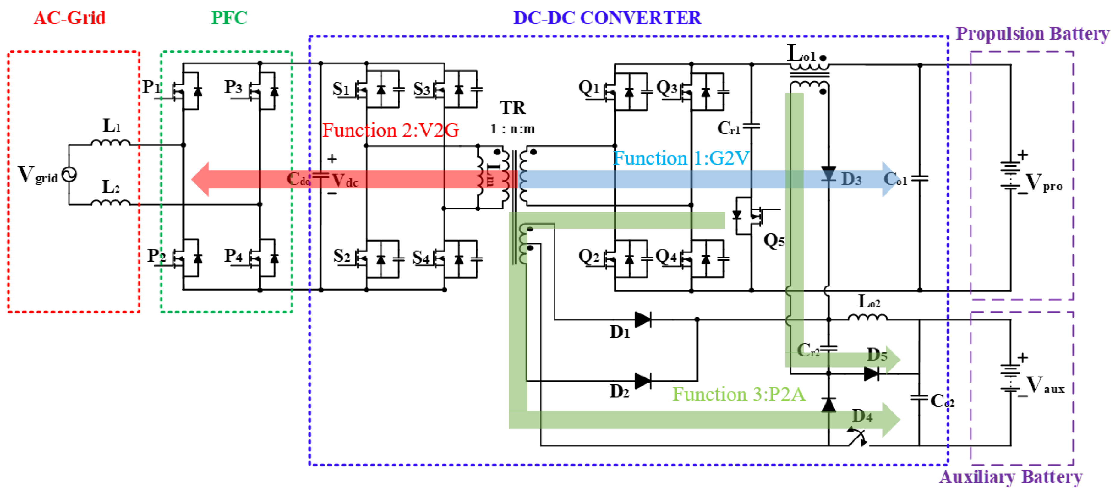
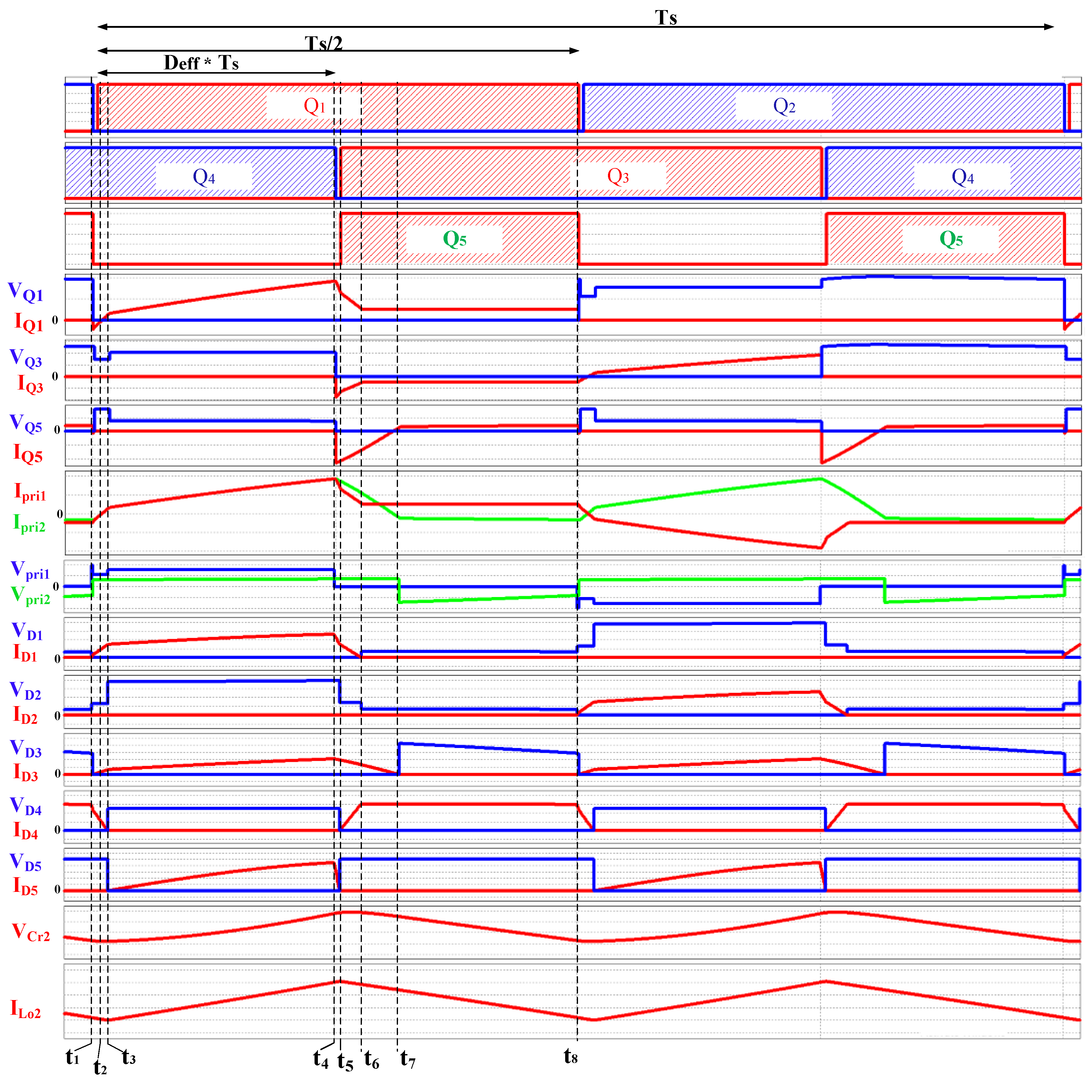
2. Operation of the Proposed Integrated OBC

The circuit diagram of the LDC converter in the proposed integrated OBC is shown in Figure 2. The primary side is composed of an input capacitor Co1, an active clamp circuit with Cr1 and an active switch Q5 and a PSFB converter with switches Q1, Q2, Q3 and Q4. The transformer of the PSFB converter is TR1 with a magnetizing inductance Lm1, a leakage inductance LLK1 and a turns ratio of n1:1. The transformer of the forward converter is TR2 with a magnetizing inductance Lm2, a leakage inductance LLK2 and a turns ratio of n2:1. The secondary side of the PSFB converter includes rectifier diodes D1 and D2, a passive snubber circuit composed of Cr2, D4 and D5. The capacitor Cr2 connected in parallel with the output inductor LO2 also plays a function as an output capacitor of the forward converter and reduces the current ripple of the output. As mentioned earlier, the focus is on explaining the operation of the LDC of the proposed integrated OBC. Here, a half of the switching cycle of the proposed converter is divided into seven modes and the operation is explained in detail since the other half is symmetric. The key waveforms and the equivalent circuits of each operation mode are shown in Figure 3 and Figure 4, respectively. For the sake of simplicity, all of the circuit components are ideal except the output capacitance of the switch and all of the output capacitances of the switches are assumed to be same.
Mode 1 [t1t2], Figure 4a.
At t = t1, Q4 is on and Q3 is off. Q2 and Q5 turn off, and their parasitic capacitors are charged. The parasitic capacitor of Q1 is discharged and its body diode is forward biased creating ZVS turn-on condition for Q1. The power is transferred to load through the transformers TR1 and TR2.
In the secondary side, diodes D2 and D5 are reverse biased. D1, D3 and D4 are forward biased. The resonant capacitor Cr2 resonates with output inductor LO2 and discharges the energy to the output.
Mode 2 [t2t3], Figure 4b.
At t = t2, Q1 turns on while Q4 is already on in mode 1. Q2, Q3 and Q5 are off. The body diode of Q1 is reverse biased and the current flows through Q1. The secondary side works in the same fashion as in mode 1. Due to the resonance between Cr2 and LO2, the current flowing through D4 decreases to zero and achieves ZCS turn-off condition for D4 at the end of this mode.
Mode 3 [t3t4], Figure 4c.
At t = t3, Q1 and Q4 are on. Q2, Q3 and Q5 are off. The input power is delivered to the output by both converters. In the forward converter, the primary current ipri2(t) flows through the transformer TR2 and charges the resonant capacitor Cr2 in the secondary side. In the PSFB converter, the primary current ipri1 flows through switches Q1, Q4 and transformer TR1. The currents ipri1 and ipri2(t) are determined as below.
i p r i 1 ( t ) = 1 n 1 ( i L O 2 ( t ) + V p r i 1 n 1 V A u x _ b a t n 1 L O 2 ( t t 1 ) )
i p r i 2 ( t ) = 1 n 2 ( i L O 2 ( t ) + V C r 2 ( t ) L O 2 ( t t 1 ) )
where Vpri1 is the primary winding voltage of the transformer TR1, Vaux_bat is the auxiliary battery voltage, ipri1 is the primary current of the forward converter, ipr2 is the primary current of the PSFB converter, iLo2 is the current flow through the output inductor Lo2, and VCr2 is the voltage of capacitor Cr2.
In the secondary side, diode D4 is reverse biased and D5 is forward biased to charge the resonant capacitor Cr2 and the output capacitor Co2, respectively. The rectifier bridge voltage Vrec(t) can be calculated as in (3).
V r e c ( t ) = V A u x _ b a t + V C r 2 ( t )
where Vrec is the rectifier voltage of the PSFB converter.
Mode 4 [t4t5], Figure 4d.
At t = t4, the switch Q4 turns off. The parasitic capacitor of Q3 is discharged. In the forward converter, the current of transformer TR2 flows through the active clamp circuit including capacitor Cr1 and the body diode of Q5. The capacitor Cr1 resonates with the leakage inductor LLK2. Since the parasitic capacitor of Q4 is charged and that of Q3 is discharged, the ZVS turn-on condition for Q3 is achieved. The voltage VCoss_Q3 across Q3 can be found as shown in (4).
V C O S S _ Q 3 = V p r i 1 ( t ) Z 1 i p r i 1 ( t 4 ) sin ω ( t t 4 )
where ω and Z1 can be calculated using (5) and (6), respectively.
ω = 1 ( L L K 1 + L m 1 ) C O S S
Z 1 = L L K 1 + L m 1 C O S S
In the secondary side, the current commutation occurs from D1 to D4 and resonant capacitor Cr2. The current iD1 flowing through D1 can be determined as follows.
i D 1 ( t ) = i L O 2 ( t 4 ) V C r 2 + V A u x _ b a t L O 2 ( t t 4 )
Mode 5 [t5t6], Figure 4e.
At t = t5, Q3 and Q5 are turned on while Q1 is on. The body diodes of Q3 and Q5 and diodes D1, D3 and D4 are forward biased. The other diodes are reverse biased. The resonant capacitor Cr2 is discharged through the diodes D1 and D4. In the forward converter, the resonance between the capacitor Cr1 and the leakage inductor LLK2 continues. The power is transferred to the secondary side through the transformer TR2 of the forward converter.
The primary current ipri1(t) of the PSFB converter can be expressed using (8).
i p r i 1 ( t ) = i m 1 ( t 5 ) = V p r i 1 L m 1 ( t t 5 )
where im1 is the magnetizing current of the PSFB converter.
The current through diode D1 can be expressed using (9).
i D 1 ( t ) = i L o 2 ( t 5 ) V A u x b a t L O 2 ( t t 5 )
Mode 6 (t6t7), Figure 4f.
At t = t6, the diode D1 is reverse biased as the current commutation from D1 to D4 is completed. In the primary side of the PSFB converter, Q1 is on and the body diode of Q3 is forward biased. The primary current of the PSFB converter is circulating and kept constant. The forward converter operates the same as in mode 5.
In the secondary side, diodes D3 and D4 are forward biased. Due to the discharge of LO2, the current through D3 decreases to zero gradually. At the end of this mode, the diode D3 is turned off with ZCS.
Mode 7 (t7t8), Figure 4g.
At t = t7, the body diode of Q5 is reverse biased and the current flows through the Q5. In the forward converter, the capacitor Cr1 resonates with the inductance of the transformer TR2 and the resonant current resets it, thereby eliminating the need for tertiary winding of the forward converter. The primary current of the PSFB converter is still circulated through the Q1 and the body diode of Q3. In this mode, there is no power transferred to the secondary side. As in mode 6, the diode D4 is still forward biased and the energy in the capacitor Cr2 is discharged to the load. After mode 7 the other half of the switching cycle operates in a symmetric fashion.

3. Features and Design Consideration

3.1. Features of the Proposed Converter

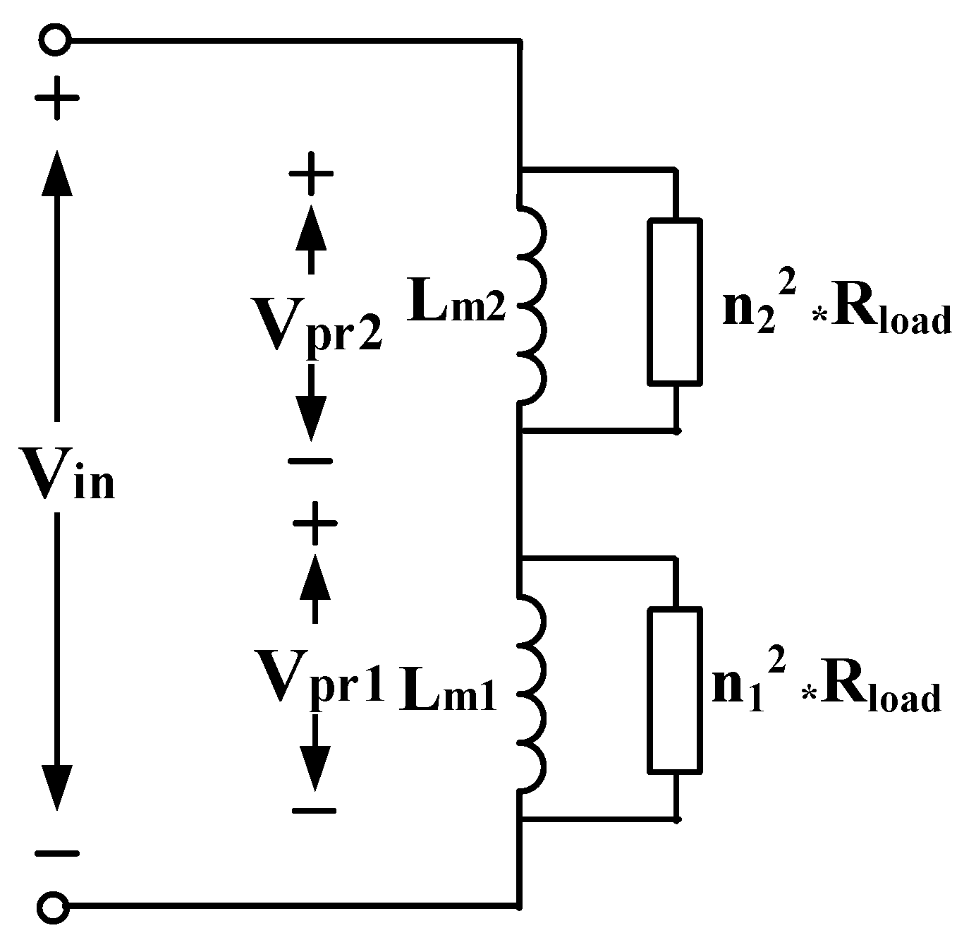
3.1.1. High Step-Down Voltage Conversion Ratio

The proposed LDC converter is a combination of a forward converter and a PSFB converter with a high step-down voltage conversion ratio as compared to the converter introduced in [24]. In order to explain the characteristics of the proposed LDC converter in terms of voltage conversion ratio its simplified circuit model is shown in Figure 5.
Based on the equivalent circuit shown in Figure 5a. the output voltage Vo of the proposed converter can be derived as (10).
V o = V p r i 1 n 1 D e f f + V p r i 2 n 2 ( D e f f + D )
where Deff is the effective duty cycle of the PSFB converter and D’ is the time period from mode 4 to mode 6 (t4t6) when the resonant capacitor Cr2 resonates with the leakage inductor LLK2 of the transformer TR2 as shown in (11).
D = 1 4 f s 2 π L L K 2 C r 2
The voltage conversion ratio of the proposed converter is decided by the turns ratio for n1 and n2 as shown in Figure 6.
The voltage applied to the primary winding of each transformer can be expressed as in (12) and (13), respectively.
V p r i 2 = n 2 2 n 1 2 + n 2 2 V i n
V p r i 1 = n 1 2 n 1 2 + n 2 2 V i n
where Vpri2 is the primary winding voltage of the transformer TR2 and VPri1 is the primary winding voltage of the transformer Tr1.
By combining (12) and (13), the voltage conversion ratio Mproposed of the proposed converter can be calculated as in (14).
M p r o p o s e d = V o V i n = 1 n 1 2 + n 2 2 ( n 1 D e f f + n 2 ( D e f f + D ) )

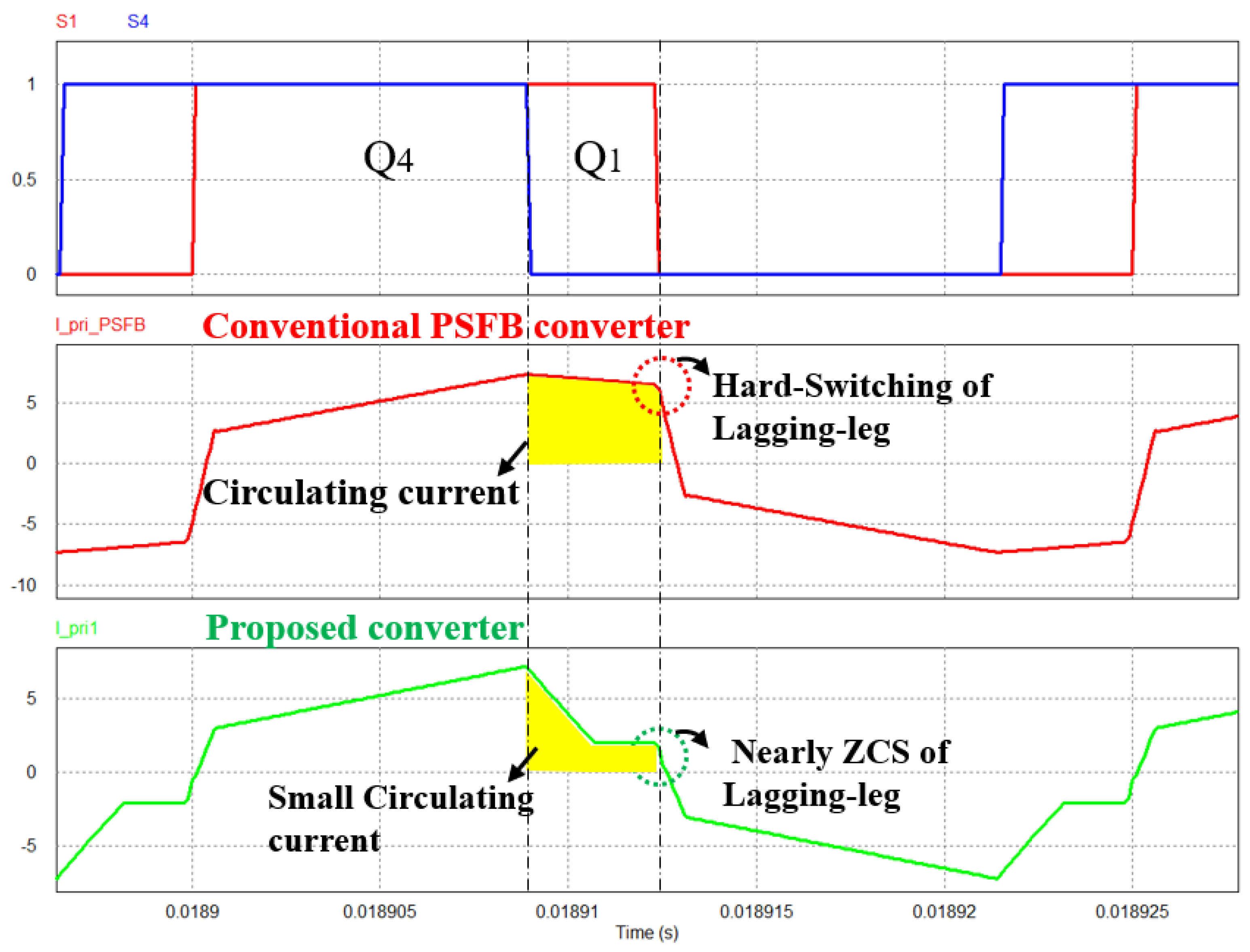
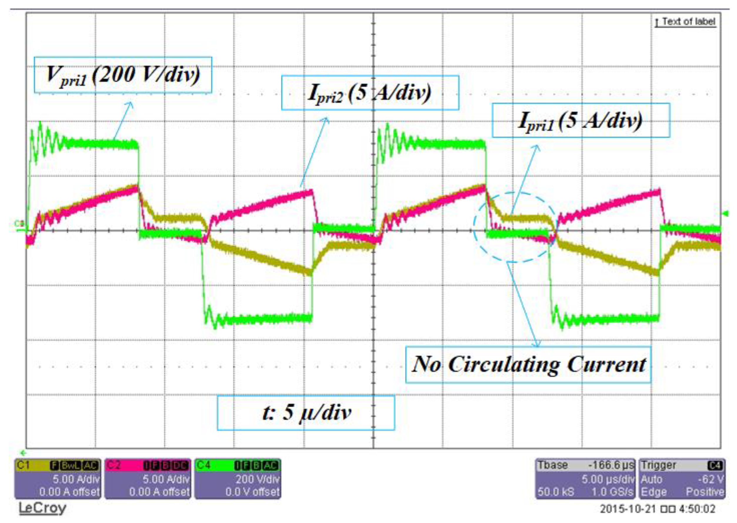
3.1.2. Elimination of the Circulating Current

In the conventional PSFB converter, the circulating current losses in the freewheeling interval reduces the power conversion efficiency, especially when the converter works with small effective duty, D. In contrast, the proposed converter can eliminate circulating current due to the additional snubber circuit composed of Cr2, D4 and D5. Figure 7 shows the difference between the circulating current in the conventional PSFB and the proposed converter. As explained in the operation of mode 4 and mode 5, since the resonant capacitor Cr2 is discharged and the diodes D1 and D4 are forward biased the primary current is reduced quickly during the freewheeling period thereby reducing the circulating current. Consequently, ZCS turn-off can nearly be achieved for the lagging leg switches of the PSFB converter.

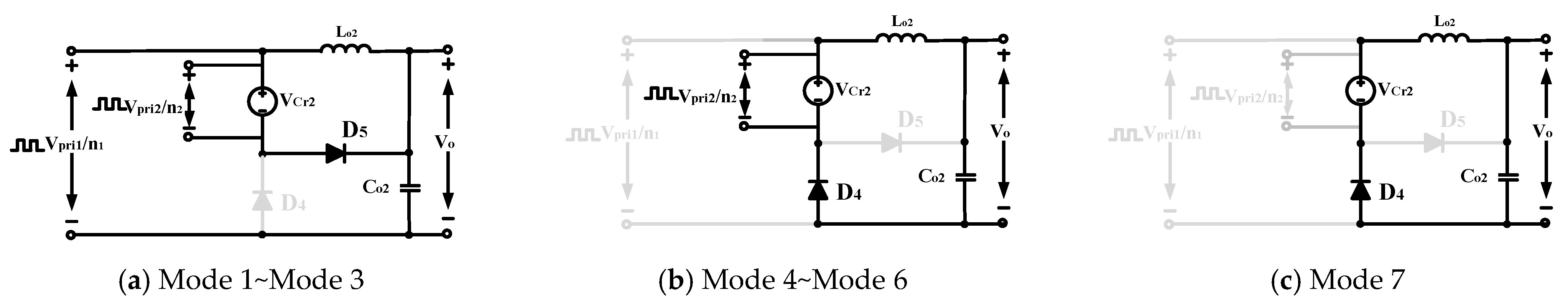
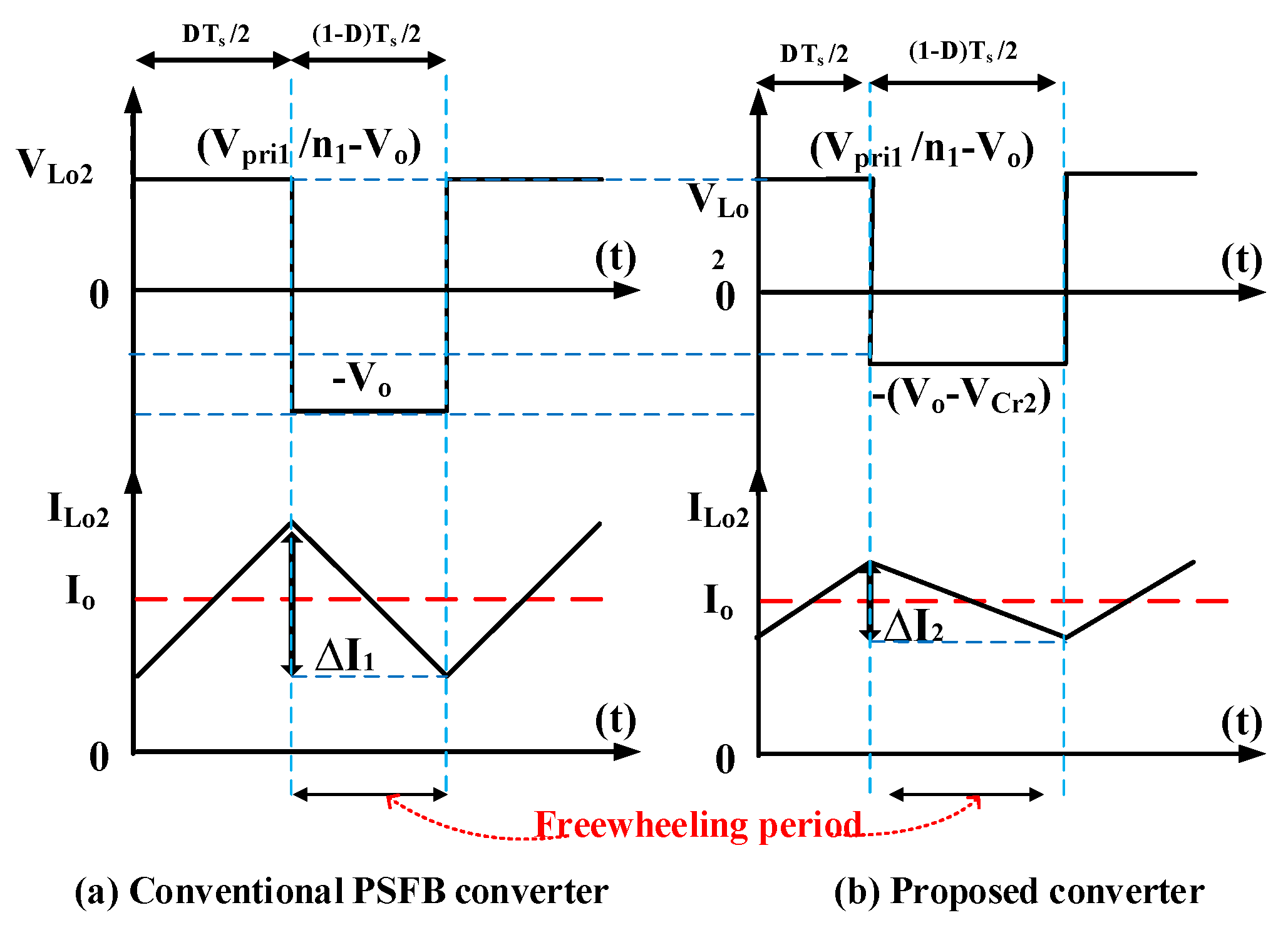
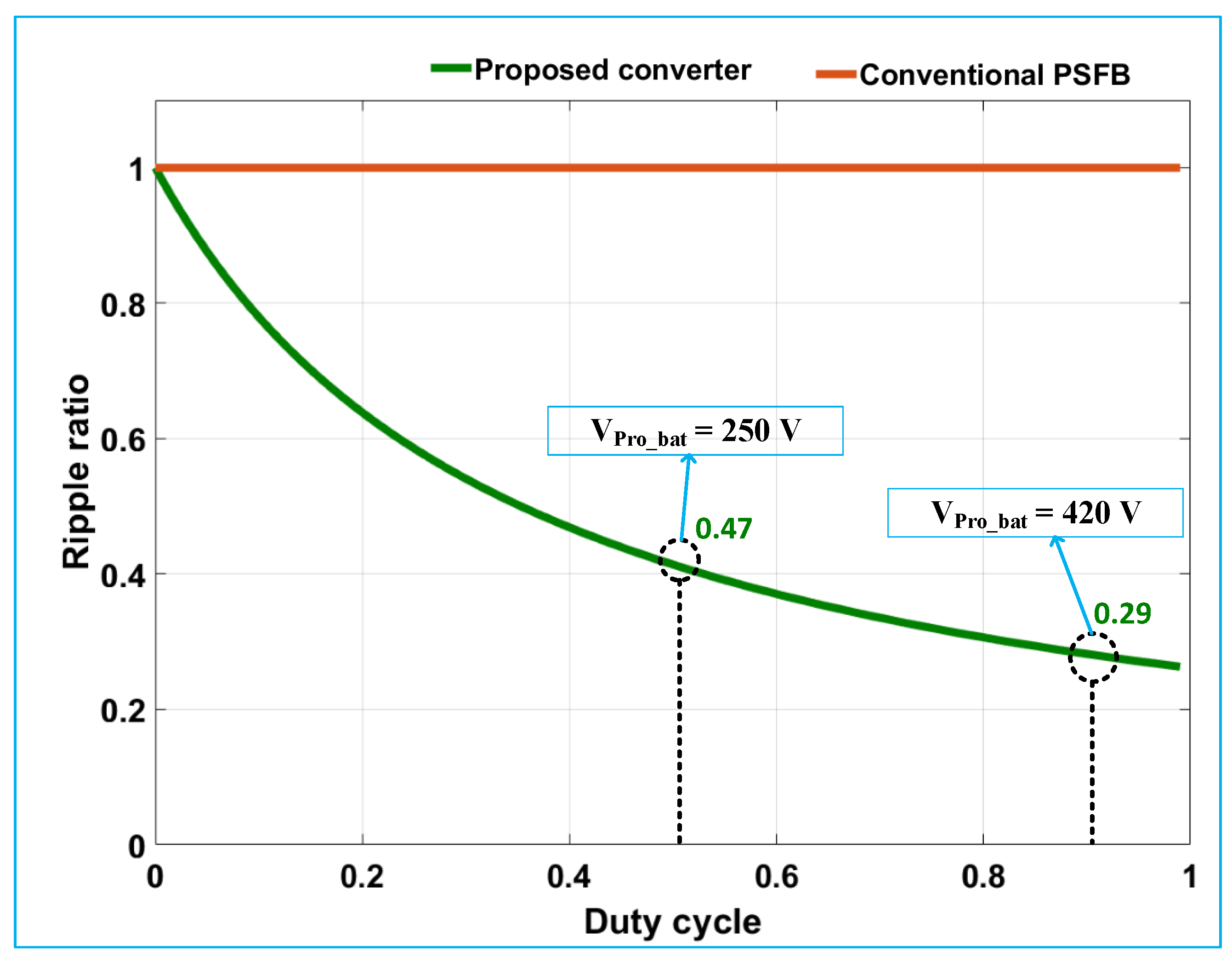
3.1.3. Small Output Current Ripple

In the conventional PSFB converter, the amplitude of the voltage applied to the output inductor in the powering period is the same as in the freewheeling period, as shown in Figure 8a. However, in the proposed converter, due to the operation of the forward converter, as explained in mode 5 to mode 7, the voltage applied to the output inductor during the freewheeling period is reduced since the diode D5 is reverse biased, as shown in Figure 8b. As a result, the current ripple of the output inductor can be reduced significantly.
In the conventional PSFB converter, the ripple current ∆I1(Conventional_PSFB) of the output inductor can be determined using (15).
Δ I 1 ( C o n v e t i o n a l _ P S F B ) = V o ( 1 D e f f ) T s 2 L o 2
The current ripple ∆I2(Proposed_Converter) of the output inductor in the proposed converter can be calculated as in (16).
Δ I 2 ( Pr o p o s e d _ C o n v e r t e r ) = ( V o V C r 2 ) ( 1 D e f f ) T s 2 L o 2
The ratio Rripple of the ripple of the current between these two cases can be calculated as in (17).
R r i p p l e = Δ I 2 Δ I 1 = V o V C r 2 V o = n 2 n 1 D e f f + n 2 ( 1 D e f f )
Figure 9 illustrates the ratio of current ripple between two cases with different values of the effective duty cycles. When the voltage of the propulsion battery is 420 V, the duty of the LDC is 0.9 and the current ripple of the output inductor LO2 of the proposed converter is just 29% of that of the conventional PSFB converter. When the voltage of the propulsion battery is 250 V, the current ripple of the output inductor LO2 is just 47% of that of the conventional PSFB converter. Therefore, the value and size of the output filter inductor LO2 can be significantly reduced.

3.2. Design Consideration

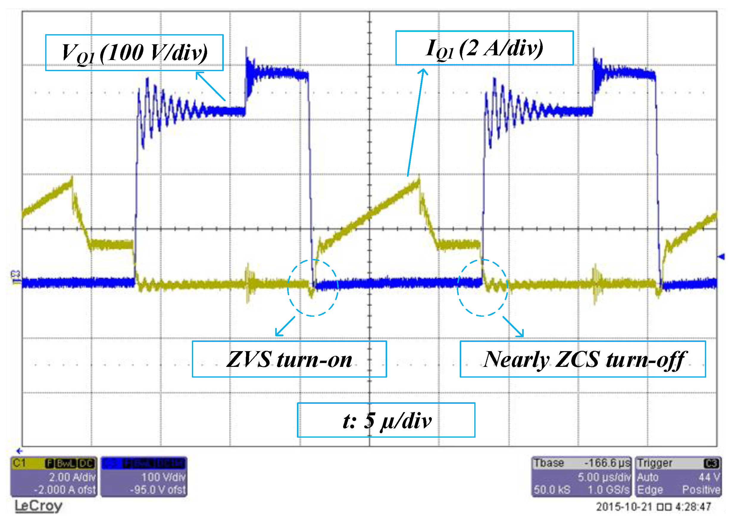
3.2.1. ZVS Conditions for All of the Switches in the PSFB over the Full Load Range

In order to achieve ZVS turn-on for MOSFETs, the magnetizing current im1 of TR1 needs to be large enough. The magnetizing current and the energy stored in the magnetizing inductance of TR1 can be determined as follows.
I m 1 , p e a k = V Pr o _ b a t L m 1 T S 4 D e f f _ min
E L m 1 = 1 2 L m 1 I m 1 , p e a k 2 = 1 2 L m 1 ( V Pr o _ b a t T S D e f f _ min 4 ) 2
where Im1,peak is the peak value of the magnetizing current of TR1. TS is the switching period and Deff_min is the minimum effective duty cycle of the PSFB converter.
To ensure the ZVS condition over the whole load range, the energy stored in the magnetizing inductance should be larger than that stored in the parasitic capacitors Coss of MOSFETs.
E L m 1 E C o s s = 1 2 ( 2 C o s s ) V Pr o _ b a t 2
The required magnetizing inductance of TR1 can be calculated as in (21).
L m 1 1 2 C o s s ( T s D e f f _ min 4 ) 2
In addition to the condition in (21), the dead-time for the MOSFETs also needs to be satisfied (22).
T d e a d π 2 2 ( L L K 1 + L L K 2 ) C o s s

3.2.2. Design of the Clamp and Resonant Capacitors

As explained earlier in the operation of mode 7, the capacitor Cr1 resonates with the leakage inductance LLK2 and the magnetizing inductance Lm2 of TR2. Hence, the value of clamp capacitor Cr1 can be calculated as in (23). However, since the voltage applied to the switches of PSFB converter increases due to the resonance, the resonant frequency needs to be selected much lower than the switching frequency in order to reduce it.
C r 1 > > 1 ( 2 π f s ) 2 ( L L K 1 + L m 1 )
The resonant capacitor Cr2 is the output capacitor of the forward converter. Thus, its value can be calculated using (24).
C r 2 > n 2 I o ( D e f f + D ) n 1 f s Δ V C r 2

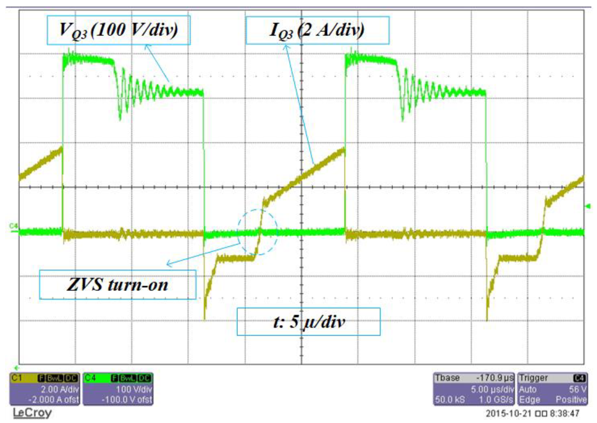
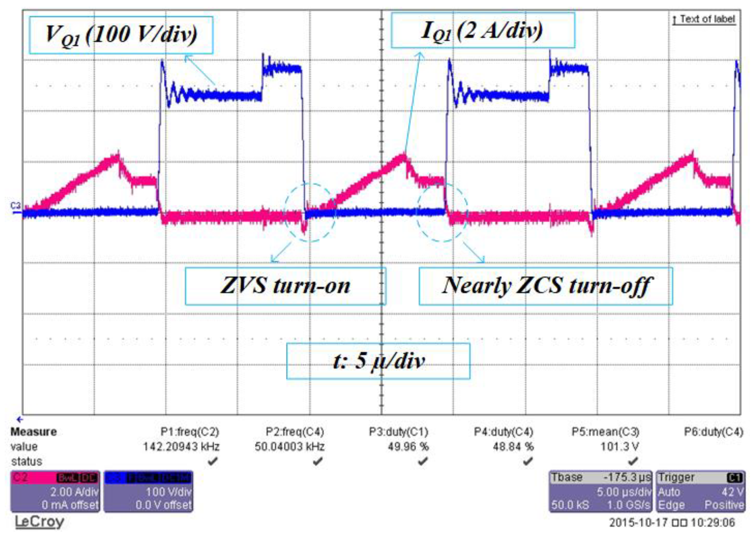
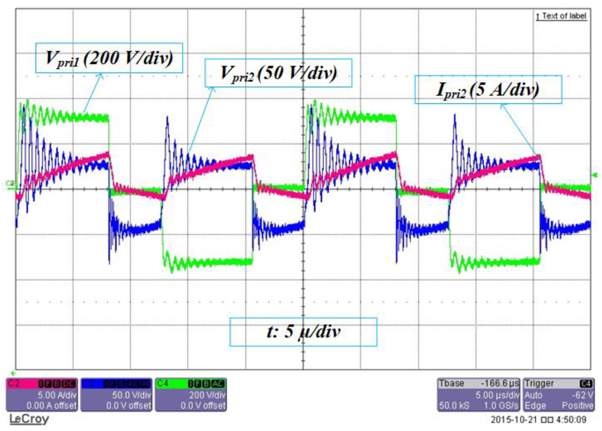
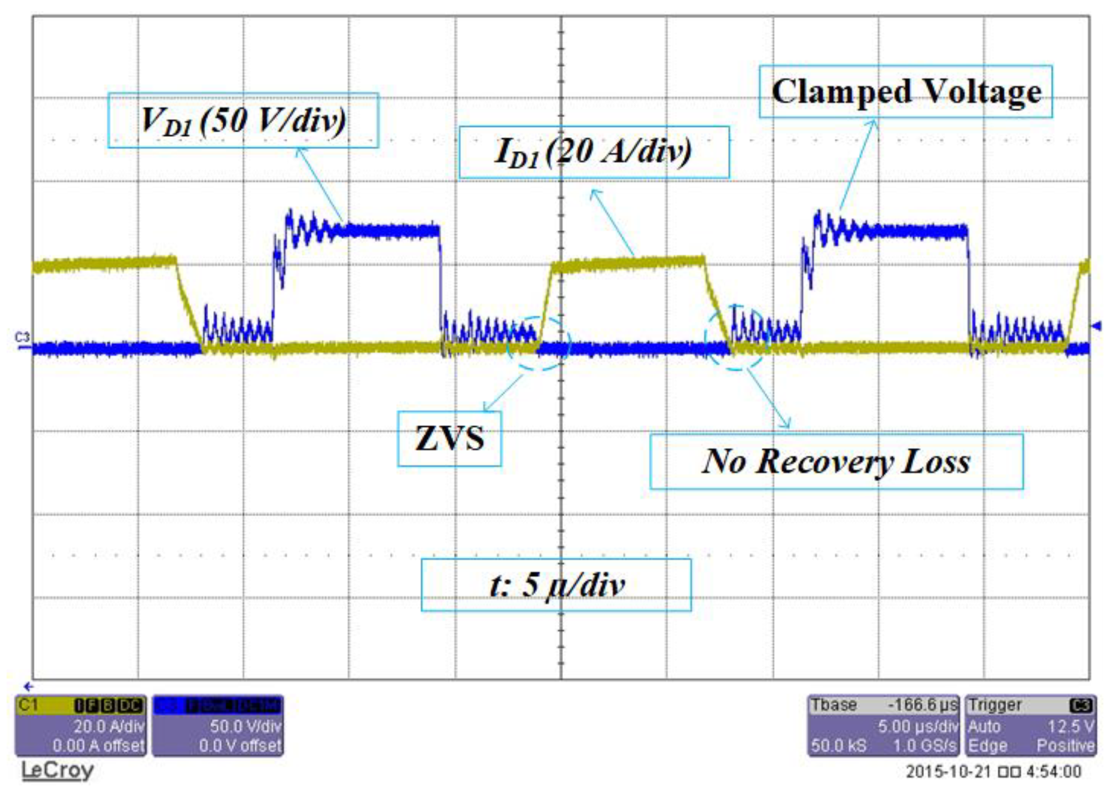
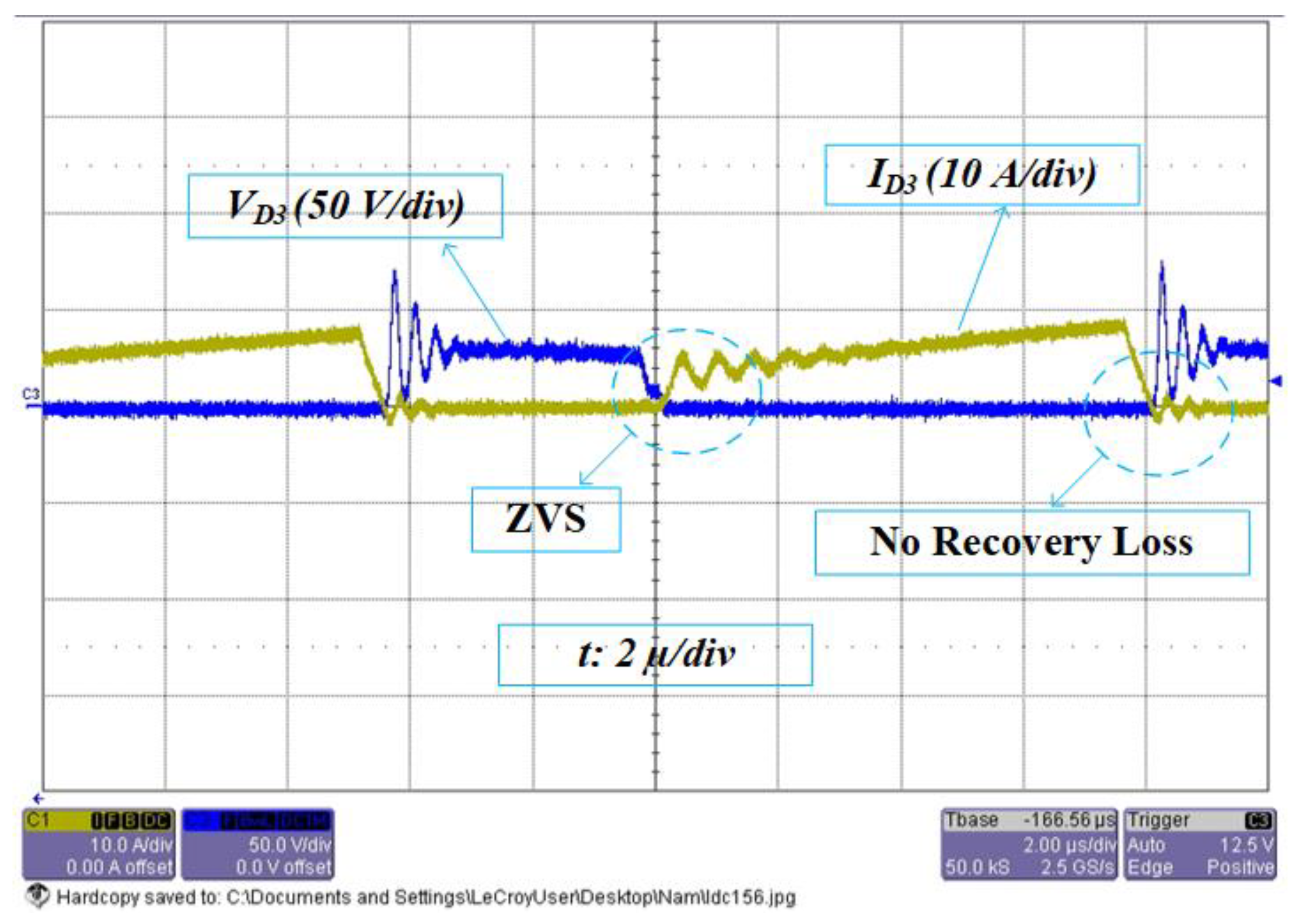
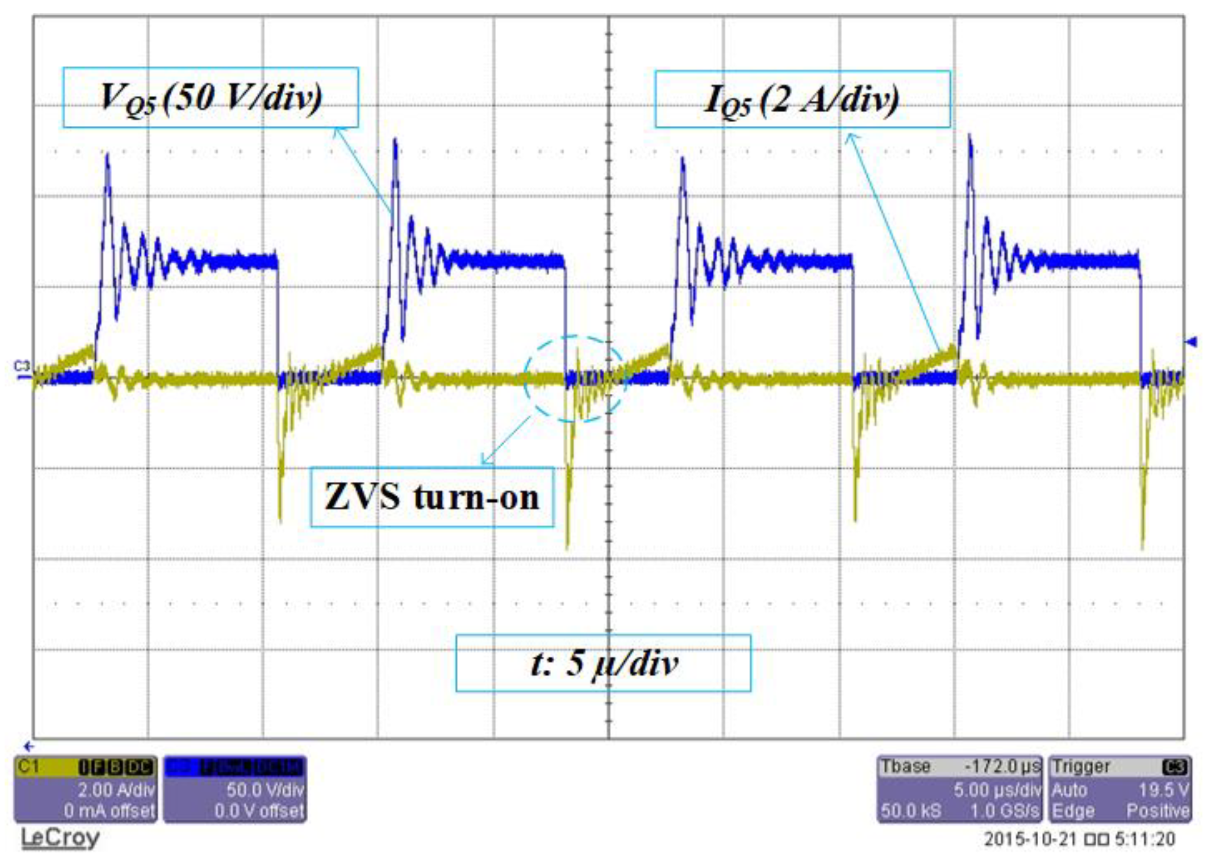
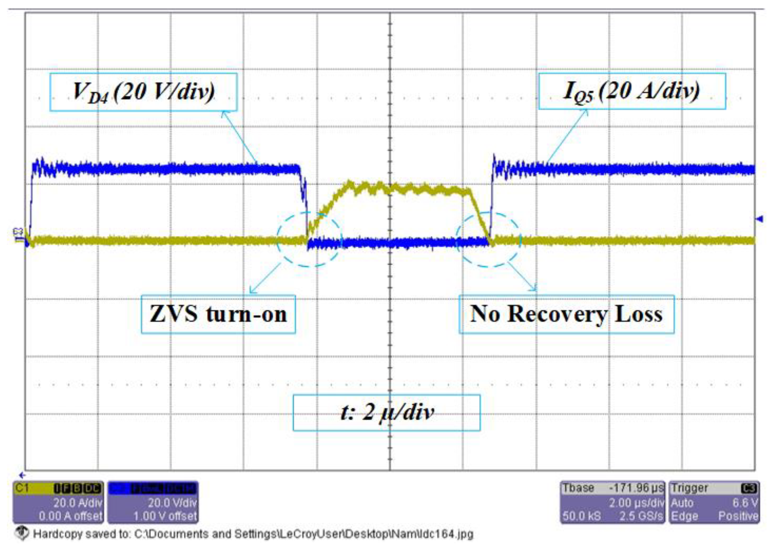
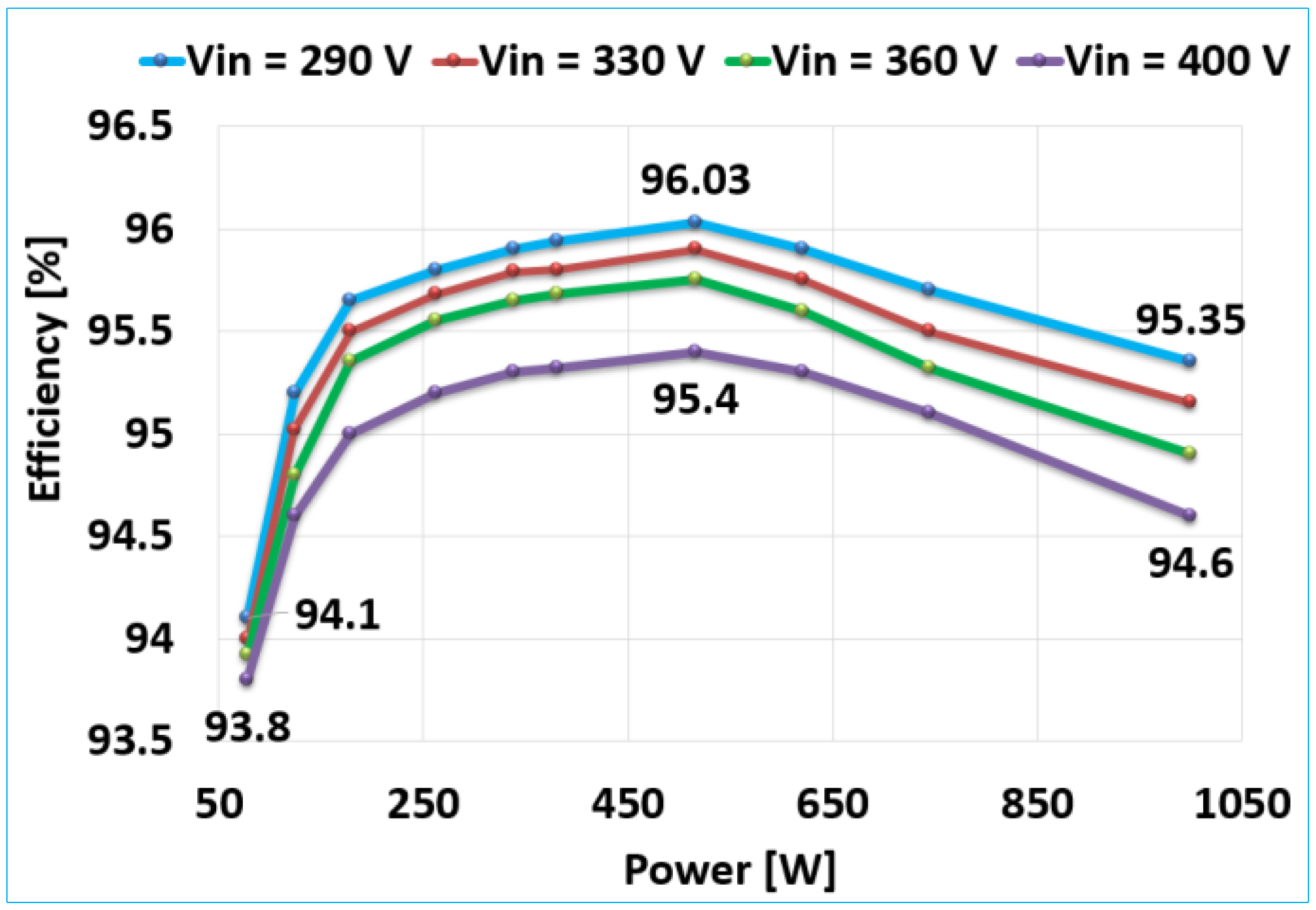
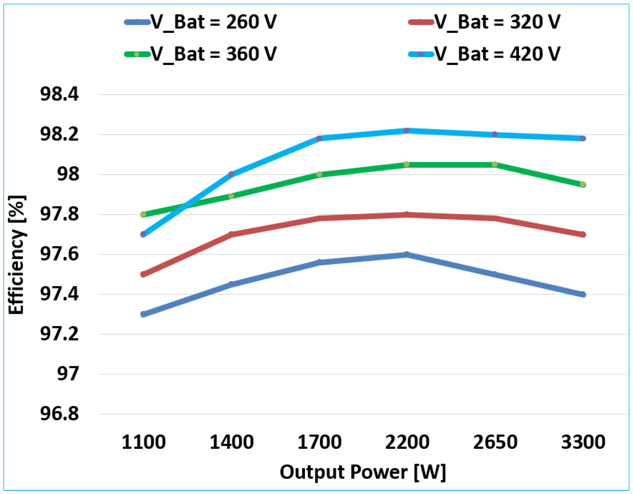
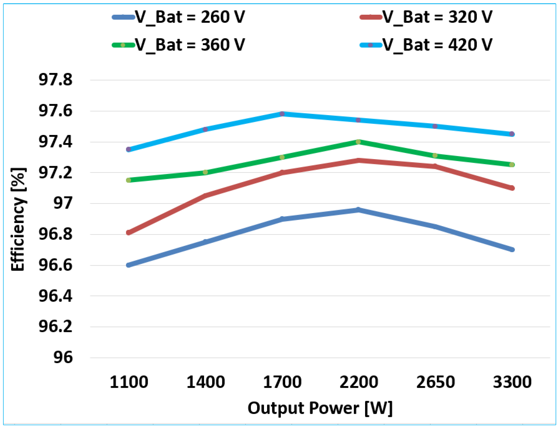
4. Experimental Results

In order to verify the performance of the proposed topology, a prototype converter was implemented. The specification of the proposed converter is shown in Table 1. All of the parameters for the transformer, inductor and capacitor are illustrated in Table 2. This paper focuses on illustrating the experimental results regarding function III of the proposed integrated OBC.
Figure 10 and Figure 11 show the measured waveforms at the lagging switches and the leading switches with 400 V input, 25 V output and 1 kW output power. In Figure 10, it can be observed that the MOSFET Q1 turns on with ZVS and turns off with nearly ZCS. There is a small negative current flowing through its body diode to maintain the zero voltage during the turn-on period. The turn-off current of Q1 is just 0.5 A, thus turn-off losses of the lagging leg MOSFETs are minimized. Figure 11 shows that MOSFET Q3 is also turned on with ZVS condition.
Figure 12 shows the waveform of MOSFET Q1 at the light load condition (10% load) with an input voltage of 330 V and output power of 100 W. It can be clearly observed from Figure 12 that the lagging leg switches can maintain ZVS turn-on and nearly ZCS turn-off at light load condition.
Figure 13 represents the voltage and current waveforms of the transformer TR1. It can be observed that there is nearly no circulating current in the primary side of the transformer TR1 during freewheeling interval.
The measured waveforms in Figure 14 depict the waveforms at the primary side of the transformer TR2. We can see that the current of transformer TR2 is reset by the active clamp circuit Q5 and Cr1. Figure 15 shows that both ZVS turn-on and ZCS turn-off can be achieved at the secondary rectifier diodes, hence there is no reverse recovery. In addition, the voltage at the rectifier diode is clamped around 80 V so that the diode with a lower voltage rating can be used.
The measured waveforms at diode D3 are shown in Figure 16. It can achieve both ZVS turn-on and ZCS turn-off. The voltage across the diode D3 oscillates due to the leakage inductance of the transformer TR2. Figure 17 shows the current and voltage waveforms at the active clamp switch Q5 with ZVS turn-on.
The measured waveforms at diode D4 are shown in Figure 18. Both ZVS turn-on and ZCS turn-off are achieved at diode D4, thus there is no recovery loss at this diode.
The efficiency during function III operation with a wide range of input voltage variation is measured and shown in Figure 19 with the wide input voltage variation from 290 V to 400 V. The proposed converter shows a high efficiency all over the load range and the maximum efficiency is 96.03% at 500 W, which is much higher than those of conventional ones in [19,22,25].
The efficiency during function I and function II operations is also shown in Figure 20 and Figure 21, respectively. In function I, the maximum efficiency is 98.2% when VDC = 400 V, VDC = 420 V and PO_I = 2.3 kW. In function II, the maximum efficiency is 97.58% when VDC = 400 V, VPro_Bat = 420 V and PO_II = 1.8 kW.

5. Conclusions

This paper has introduced a novel hybrid LDC converter for the integrated OBC using a combination of a PSFB converter and a forward converter. The proposed converter has a high voltage conversion ratio and a high efficiency characteristic due to the hybrid structure. The power is shared by two converters and hence the conduction loss is reduced. The efficiency of the proposed converter can be further improved due to the soft-switching characteristics throughout the load range. The proposed integrated OBC shows over 97% efficiency during function I operation, over 96% efficiency during function II operation and over 95% efficiency during function III operation almost throughout the load range, respectively. In addition, the size of the output inductor can be reduced significantly due to the cascaded output capacitors of the proposed LDC converter. The circulating current is reduced by using the passive snubber circuit, which also helps clamp the voltage applied to the rectifier diodes. The cost and the volume of the OBC can be significantly reduced due to the integrated structure of the proposed converter, and the fuel economy of the electric vehicles can be improved due to its high efficiency characteristics throughout the load range.

Author Contributions

V.-H.N. wrote the original draft manuscript and designed the prototype of the proposed converter; D.-V.T. analyzed the proposed converter and revised the manuscript; W.C. reviewed the manuscript and supervised the research. All authors have read and agreed to the published version of the manuscript.

Funding

This research received no external funding.

Institutional Review Board Statement

Not applicable.

Informed Consent Statement

Not applicable.

Conflicts of Interest

The authors declare no conflict of interest.

References

  1. He, T.; Lu, D.D.-C.; Wu, M.; Yang, Q.; Li, T.; Liu, Q. Four-Quadrant Operations of Bidirectional Chargers for Electric Vehicles in Smart Car Parks: G2V, V2G, and V4G. Energies 2021, 14, 181. [Google Scholar] [CrossRef]
  2. Figueiredo, J.P.M.; Tofoli, F.L.; Silva, B.L.A. A Review of Single-Phase PFC Topologies Based on the Boost Converter. In Proceedings of the 2010 9th IEEE/IAS International Conference on Industry Applications-INDUSCON 2010, Sao Paulo, Brazil, 8–10 November 2010; pp. 1–6. [Google Scholar] [CrossRef]
  3. Musavi, F.; Eberle, W.; Dunford, W.G. A High-Performance Single-Phase Bridgeless Interleaved PFC Converter for Plug-in Hybrid Electric Vehicle Battery Chargers. IEEE Trans. Ind. Appl. 2011, 47, 1833–1843. [Google Scholar] [CrossRef]
  4. Musavi, F.; Eberle, W.; Dunford, W.G. A Phase Shifted Semi-Bridgeless Boost Power Factor Corrected Converter for Plug in Hybrid Electric Vehicle Battery Chargers. In Proceedings of the 2011 Twenty-Sixth Annual IEEE Applied Power Electronics Conference and Exposition (APEC), Fort Worth, TX, USA, 6–11 March 2011; pp. 821–828. [Google Scholar] [CrossRef]
  5. Singh, B.; Singh, B.N.; Chandra, A.; Al-Haddad, K.; Pandey, A.; Kothari, D.P. A review of single-phase improved power quality AC-DC converters. IEEE Trans. Ind. Electron. 2003, 50, 962–981. [Google Scholar] [CrossRef] [Green Version]
  6. Gautam, D.; Musavi, F.; Edington, M.; Eberle, W.; Dunford, W.G. An Automotive on-Board 3.3 kW Battery Charger for PHEV Application. In Proceedings of the 2011 IEEE Vehicle Power and Propulsion Conference, Chicago, IL, USA, 6–9 September 2011; pp. 1–6. [Google Scholar] [CrossRef]
  7. Gautam, D.S.; Musavi, F.; Eberle, W.; Dunford, W.G. A Zero-Voltage Switching Full-Bridge DC-DC Converter with Capacitive Output Filter for Plug-In Hybrid Electric Vehicle Battery Charging. IEEE Trans. Power Electron. 2013, 28, 5728–5735. [Google Scholar] [CrossRef]
  8. Averberg, A.; Meyer, K.R.; Mertens, A. Current-Fed Full Bridge Converter for Fuel Cell Systems. In Proceedings of the 2008 IEEE Power Electronics Specialists Conference, Rhodes, Greece, 15–19 June 2008; pp. 866–872. [Google Scholar] [CrossRef]
  9. Yakushev, V.; Meleshin, V.; Fraidlin, S. Full-Bridge Isolated Current Fed Converter with Active Clamp. In Proceedings of the APEC ’99. Fourteenth Annual Applied Power Electronics Conference and Exposition. 1999 Conference Proceedings (Cat. No.99CH36285), Dallas, TX, USA, 14–18 March 1999; Volume 1, pp. 560–566. [Google Scholar] [CrossRef]
  10. Choi, H.S.; Kim, J.W.; Cho, B.H. Novel zero-voltage and zero-current-switching (ZVZCS) full-bridge PWM converter using coupled output inductor. IEEE Trans. Power Electron. 2002, 17, 641–648. [Google Scholar] [CrossRef]
  11. Dudrik, J.; Trip, N. Soft-Switching PS-PWM DC–DC Converter for Full-Load Range Applications. IEEE Trans. Ind. Electron. 2010, 57, 2814. [Google Scholar] [CrossRef]
  12. Cho, J.G.; Rim, G.H.; Lee, F.C. Zero Voltage and Zero Current Switching Full Bridge PWM Converter using Secondary Active Clamp. In Proceedings of the PESC Record. 27th Annual IEEE Power Electronics Specialists Conference, Baveno, Italy, 23–27 June 1996; Volume 1, pp. 657–663. [Google Scholar] [CrossRef]
  13. Zhang, X.; Chung, H.S.; Ruan, X.; Ioinovici, A. A ZCS Full-Bridge Converter without Voltage Overstress on the Switches. IEEE Trans. Power Electron. 2010, 25, 686–698. [Google Scholar] [CrossRef]
  14. Tran, D.; Vu, N.; Choi, W. A Quasi-Resonant ZVZCS Phase-Shifted Full-Bridge Converter with an Active Clamp in the Secondary Side. Energies 2018, 11, 2868. [Google Scholar] [CrossRef] [Green Version]
  15. Hiltunen, J.; Väisänen, V.; Juntunen, R.; Silventoinen, P. Variable-Frequency Phase Shift Modulation of a Dual Active Bridge Converter. IEEE Trans. Power Electron. 2015, 30, 7138–7148. [Google Scholar] [CrossRef]
  16. Park, J.; Choi, S. Design and Control of a Bidirectional Resonant DC–DC Converter for Automotive Engine/Battery Hybrid Power Generators. IEEE Trans. Power Electron. 2014, 29, 3748–3757. [Google Scholar] [CrossRef]
  17. Oh, C.; Kim, D.; Woo, D.; Sung, W.; Kim, Y.; Lee, B. A High-Efficient Nonisolated Single-Stage On-Board Battery Charger for Electric Vehicles. IEEE Trans. Power Electron. 2013, 28, 5746–5757. [Google Scholar] [CrossRef]
  18. Yoo, K.; Kim, K.; Lee, J. Single- and Three-Phase PHEV Onboard Battery Charger Using Small Link Capacitor. IEEE Trans. Ind. Electron. 2013, 60, 3136–3144. [Google Scholar] [CrossRef]
  19. Nguyen, H.V.; Lee, D.-C.; Blaabjerg, F. A Novel SiC-Based Multifunctional Onboard Battery Charger for Plug-In Electric Vehicles. IEEE Trans. Power Electron. 2021, 36, 5635–5646. [Google Scholar] [CrossRef]
  20. Nguyen, H.V.; To, D.; Lee, D. Onboard Battery Chargers for Plug-in Electric Vehicles With Dual Functional Circuit for Low-Voltage Battery Charging and Active Power Decoupling. IEEE Access 2018, 6, 70212–70222. [Google Scholar] [CrossRef]
  21. Nguyen, H.V.; Lee, D. An Improved Low-Voltage Charging Circuit for Single-Phase Onboard Battery Chargers. In Proceedings of the 2019 IEEE Applied Power Electronics Conference and Exposition (APEC), Anaheim, CA, USA, 17–21 March 2019; pp. 3325–3331. [Google Scholar] [CrossRef]
  22. Kim, D.; Kim, M.; Lee, B. An Integrated Battery Charger with High Power Density and Efficiency for Electric Vehicles. IEEE Trans. Power Electron. 2017, 32, 4553–4565. [Google Scholar] [CrossRef]
  23. Kim, S.; Kang, F. Multifunctional Onboard Battery Charger for Plug-in Electric Vehicles. IEEE Trans. Ind. Electron. 2015, 62, 3460–3472. [Google Scholar] [CrossRef]
  24. Kim, S.Y.; Song, H.; Nam, K. Idling Port Isolation Control of Three-Port Bidirectional Converter for EVs. IEEE Trans. Power Electron. 2012, 27, 2495–2506. [Google Scholar] [CrossRef]
  25. Kim, Y.; Oh, C.; Sung, W.; Lee, B.K. Topology and Control Scheme of OBC–LDC Integrated Power Unit for Electric Vehicles. IEEE Trans. Power Electron. 2017, 32, 1731–1743. [Google Scholar] [CrossRef]
Figure 1. Proposed integrated OBC.
Energies 14 03603 g001
Figure 2. LDC converter of the proposed integrated OBC.
Energies 14 03603 g002
Figure 3. Key waveforms of proposed LDC converter.
Energies 14 03603 g003
Figure 4. Equivalent circuits of proposed LDC converter.
Energies 14 03603 g004
Figure 5. Simplified circuit model of the LDC converter: (a) power transfer mode in both converters, (b) power transfer mode in forward converter and freewheeling mode of PSFB converter, (c) freewheeling mode of both converters.
Energies 14 03603 g005
Figure 6. Equivalent circuit to show the voltage conversion ratio of the proposed LDC.
Energies 14 03603 g006
Figure 7. Comparison of the circulating current in the conventional PSFB converter and proposed converter.
Energies 14 03603 g007
Figure 8. Voltage and current waveforms at the output inductor of the conventional PSFB converter and the proposed converter.
Energies 14 03603 g008
Figure 9. The ratio of the current ripple of the proposed converter compared to the conventional topology.
Energies 14 03603 g009
Figure 10. Voltage and current of switch Q1 at 100% of load.
Energies 14 03603 g010
Figure 11. Voltage and current of switch Q3 at 100% of load.
Energies 14 03603 g011
Figure 12. Voltage and current of switch Q1 at 10% of load.
Energies 14 03603 g012
Figure 13. Voltage and current of transformer T R 1 at 100% of load.
Energies 14 03603 g013
Figure 14. Voltage and current of transformer T R 2 at 100% of load.
Energies 14 03603 g014
Figure 15. Voltage and current of diode D 1 at 100% of load.
Energies 14 03603 g015
Figure 16. Voltage and current of diode D 3 at 100% of load.
Energies 14 03603 g016
Figure 17. Voltage and current of switch Q 5 at 100% of load.
Energies 14 03603 g017
Figure 18. The voltage and current of diode D 4 at 100% of load.
Energies 14 03603 g018
Figure 19. Efficiency plots during function III operation with wide range of input voltage variation.
Energies 14 03603 g019
Figure 20. Efficiency plots during function I operation with wide range of input voltage variation.
Energies 14 03603 g020
Figure 21. Efficiency plots during function II operation with wide range of input voltage variation.
Energies 14 03603 g021
Table 1. Specification for the integrated OBC converter.
Operation ConditionParameterValue [Unit]
PFC stageAC voltage220 [V]/60 [Hz]
DC-link Voltage380–420 [V]
Rated power3.5 [kW]
Function I:
DC-link to propulsion battery
DC-link voltage380–420 [V]
Propulsion battery voltage250–420 [V]
Rated power3.3 [kW]
Switching frequency30 [kHz]
Function II:
Propulsion battery to DC-link (OBC)
DC-link voltage380–420 [V]
Propulsion battery voltage250–420 [V]
Rated power3.3 [kW]
Switching frequency30 [kHz]
Function III:
Propulsion battery to auxiliary battery (LDC)
Propulsion battery voltage250–420 [V]
Auxiliary battery voltage23–25 [V]
Rated power1 [kW]
Switching frequency50 [kHz]
Table 2. Parameters of the circuit components.
ComponentsValue
All Switches ( S 1 ~ S 4 : Q 1 ~ Q 5 )IPW65R041CFD
Turns ratio of the transformer TR1 (1:n:m)20:23:3
Leakage inductance of transformer TR1 (LLK1)12.2 [µH]
Magnetizing inductance of transformer TR1 (Lm1)605 [µH]
Core size of TR1PQ72/52
Turns ratio of the transformer TR2 (n2)32:16
Leakage inductance of transformer TR2 (LLK2)16 [µH]
Magnetizing inductance of transformer TR2 (Lm2)452 [µH]
Core size of TR1PQ72/52
Clamp capacitor (Cr1)0.22 [µF]
Resonant capacitor (Cr2)100 [µF]
Diodes ( D 1 ~ D 2 )DSSK 70-008A
Diode ( D 3 ~ D 5 )DSSK 60-0045B
Publisher’s Note: MDPI stays neutral with regard to jurisdictional claims in published maps and institutional affiliations.

