Abstract
Recent Modular Multilevel Converter (MMC) topology allows for drastic improvements in power electronic conversion such as higher energy quality, lower power semiconductors electrical stress, decreased Electro-Magnetic Interferences (EMI), and reduced switching losses. MMC is widely used in High Voltage Direct-Current (HVDC) transmissions as it offers, theoretically, no voltage limit. However, its control electronic structure is not modular itself. Especially, the insulation voltage between the submodule gate drivers’ primaries and secondaries depends on the number of submodules. The converter voltage levels cannot be increased without designing all gate driver isolations again. To solve that issue, the novel concept of distributed galvanic insulation is introduced for multilevel converters. The submodule’s gate drivers are daisy-chained, which naturally reduces the insulation voltage to the submodule capacitor voltage, regardless of the number of submodules. The MMC becomes truly modular as the number of submodules can be increased without impacting on the previous control electronic circuit. Such an innovative control structure weakens the link between the main control unit and the gate drivers. This inherent structural problem can be solved through the use of Smart-Gate Drivers (SGD), as they are often equipped with fast and bidirectional communication channels, while highly increasing the converter reliability. The innovation proposed in that work is the involvement of smart gate drivers in the distributed galvanic insulation-based MMC control and monitoring. First, the numerous benefits of smart gate drivers are discussed. Then, an innovative Voltage Balancing Algorithm directly integrated on the chained gate drivers is proposed and detailed. It features a tunable parameter, offering a trade-off between accurate voltage balancing and execution time. The proposed embedded algorithm features a low execution time due to simultaneous voltage comparisons. Such an algorithm is executed by the gate drivers themselves, relieving the main control unit in an original decentralized control scheme. A simulation model of a multi-megawatts three-phase grid-tied MMC inverter is realized, allowing validation of the proposed algorithm. Matlab/Simulink logic blocs allow us to simulate a typical CPLD/FPGA component, often embedded on smart gate drivers. The converter with the proposed embedded algorithm is simulated in steady-state and during load impact. The controlled delay and slew rate inferred by the algorithm do not disturb the converter behavior, allowing its conceptual validation.
1. Introduction
One remarkable cascaded topology had been introduced at the beginning of the century by Marquardt and Lesnicar [1], called Modular Multilevel Converter (MMC). It is the first truly modular topology with a common DC bus (i.e., its structure can be expanded in order to reach, theoretically, any arbitrary high voltage). The MMC quickly became a highly suitable choice for high power conversion. Its main applications are High Voltage Direct-Current (HVDC) links, and offshore wind farms [2,3]. For instance, the Trans-Bay Cable, inaugurated in November 2010 in San Francisco Bay, is the first HVDC link with Modular Multilevel Converters [4]. Industrials like Siemens integrate the MMC topology in drive control products [5] and STATCOM applications are also studied as the MMC offers superior controllability compared to other cascaded topologies [6]. The Modular Multilevel Converter (MMC) is based on the assembly of smaller conversion units, often called submodules (SM) or cells. One MMC phase, or “leg”, is composed of an “upper arm (U)” and a “lower arm (L)”. Each arm is constituted of a chain of N submodules in series, terminated by an inductor LARM. The AC side of the converter is at the middle point of each phase (A, B, C). The three-phase MMC is given in Figure 1. Various submodule topologies have been introduced in the literature [7,8]. The most commonly studied topologies are the Half-Bridge SubModule (HB-SM) and the H-Bridge SubModule (H-SM). Because it remains the most common structure for MMC, a focus is done on the simple Half-Bridge SubModule, given inFigure 1. Each Submodule is composed of two power transistors (or power modules) T1 and T2, usually an Insulated Gate Bipolar Transistor (IGBT) or Metal Oxide Semiconductor Field Effect Transistor (MOSFET). The submodule capacitor is charged up to a voltage VC. The submodule output voltage equals VC when T1 is closed, and 0 V when T2 is closed. The submodule is said to be inserted in the first case and bypassed in the second one.
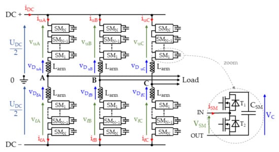
Figure 1.
Three-phase MMC converter and Half-Bridge submodule.
The MMC has been thoroughly studied in the past two decades. Various MMC models have been introduced in literature [9,10]. The number of submodules can reach several hundred in high voltage applications like HVDC [11]. The actual limitation of the submodule number is mostly based on cost and volume. Different approaches for MMC control have also been proposed, which can mainly be divided into two approaches. The first approach is based on a unique main controller for the whole converter [12,13,14], while the other uses a master/slave control scheme [15,16,17]. The conventional centralized control is based on one main controller, typically a DSP, with, usually, an auxiliary FPGA in charge of the capacitor Voltage Balancing Algorithm (VBA), as initially proposed in [1]. In [12], a control scheme is proposed using non-ideal proportional resonant controllers. The converter parasitic harmonic currents are efficiently suppressed, even in the case of a submodule fault. A tracking control is used in [13] with only one PI to tune. Model Predictive Control (MPC) is also applied to MMC [14], with a higher calculation burden on the main controller. A typical centralized control scheme with external voltage balancing is presented in Figure 2.
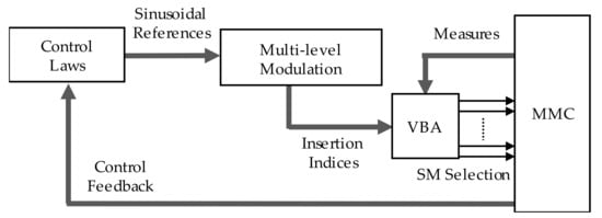
Figure 2.
MMC general centralized control architecture with external voltage balancing algorithm.
As in [14], the VBA can be embedded in the control laws and no external hardware is required. With such centralized control methods, the main controller manages all the computational burden. Another control approach uses one master controller and several slave controllers with dedicated control and/or modulation tasks. In [15], local controllers are implemented close to each submodule. These slave controllers are dedicated to the submodule capacitor voltages’ control and protection. To reduce the number of external slave controllers, submodules are grouped in [16]. Each slave controller is in charge of a submodule group, which expands the modularity of the control structure. In the control structure proposed in [17], each slave controller communicates with two other slave controllers in a loop scheme. Each cell generates its own triangular carrier dynamically, and supervises its capacitor voltage. In the case of a submodule failure, the carriers are automatically re-arranged. A general decentralized control scheme is given in Figure 3. The p slave controllers can be connected together.
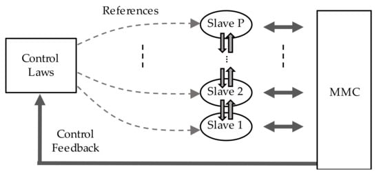
Figure 3.
MMC general decentralized control architecture with p slave controllers.
The main issue with a decentralized control is the high number of additional control hardware compared to a conventional control. The innovative gate driver structure introduced in that work allows the submodules’ intelligent gate drivers to be part of the converter control without requiring additional slave controllers. Furthermore, that novel structure allows for drastically reducing the isolation voltage of the gate drivers. This allows the integration of Smart Gate Drivers (SGD) in medium and high voltage multilevel converters, increasing both the safety and the reliability of the power modules). The scope of this paper is to emphasize the benefits of SGD in MMC structures and to involve the gate drivers in the converter control. To that extent, an innovative timing-based decentralized voltage balancing algorithm is proposed. It is directly integrated into the gate drivers and requires no external hardware.
The proposed paper is structured as follows. In Section 2, the Distributed Galvanic Insulation (DGI) is introduced. Its benefits and drawbacks are discussed. The integration of Smart-Gate Drivers in the MMC structure positively impacts the converter power modules’ reliability and safety. Through the use of Smart-Gate Drivers, a decentralized VBA is proposed in Section 3 which requires very little processing power. Its performances are demonstrated via a simulation in Section 4. Finally, a perspective of that work will be discussed in the last section.
2. MMC Decentralized Control with Smart-Gate Drivers
2.1. The Half-Bridge Modular Multilevel Converter
The chopper cell in Figure 1 uses complementary power modules and a typical built-in two-channel driver (Figure 4) is suited for the HB-SM. Such a driver is composed of a primary side, separated from two complementary secondary channels by galvanic isolation. The primary side manages the switching signals and typically ensures that both transistors are not conducting together at the same time. The secondary channels, usually called TOP and BOT (Bottom), are in charge of the close gate control of the chopper switches, along with their safe operations. The primary side communicates with the main control unit through a link usually referenced to the ground, mainly for safety reasons. However, the secondary channels are referenced to the emitter/source of the power transistors, which can be at a high potential compared to the ground. Furthermore, high EMI is generated at the secondary side due to the high dv/dt and di/dt produced by the switchings. In order to maintain that the control side is isolated from the power side, the galvanic insulation needs to withstand the voltage between the ground and the converter potentials and must present the lowest possible parasitic conductance. Optical components are the perfect candidate for such applications as they allow extremely high insulation voltages with near-zero parasitic conductance. However, isolated optical devices are not bi-directional and cannot transmit power. Hence, the secondary sides are, in most cases, powered by DC-DC isolated converters with magnetic components, which can be hard to integrate for high-power converters with high galvanic insulation voltages [18,19]. For that reason, built-in gate drivers with two channels proposed by the main manufacturers don’t reach more than 10 kV [20,21]. As power plants can reach several kilovolts, industrial built-in two-channel drivers cannot be used to drive MMC submodules.
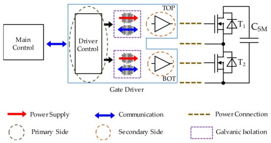
Figure 4.
Typical two-channel built-in gate driver for HB-SM with complementary switches.
Recently, Smart Gate Drivers had been introduced in the literature [22,23,24,25]. Such drivers are able to realize complex tasks, like power module monitoring, improved fault protection, detailed fault diagnosis, or active gate driving. Active gate driving (AGD) is based on the shaping of power modules’ gate voltage in order to control the switching losses, overshoot current, miller plateau duration, etc. It has already shown promising results in the literature. In [26], a turn-on gate voltage is shaped in order to increase up to 8% of the power capacity of an IGBT. The voltage overshoots are limited, which decreases the component’s electrical stress. An active gate driver is proposed in [27] with a crosstalk suppression circuit. An overcurrent protection circuit is proposed in [28] and implemented on a smart gate driver. In [29], an active gate driving circuit is proposed based on di/dt and dv/dt feedback. This circuit allows for a reduction of the current overshoot at turn on and voltage overshoot at turn off, without impacting the turn on/off and Miller plateau durations. A power IGBT switching losses are experimentally reduced up to 56% at turn on, and up to 31% at turn off. An adaptive switching profile is proposed in [30] by sensing an IGBT emitter current, and a collector to the emitter voltage. An FPGA is in charge of the gate signal shaping. The turn-on and turn-off losses can be adjusted and accurately tracked by the FPGA with PI control in few iterations. Another FPGA-based gate driver is proposed in [31]. A 63-level gate waveform can be generated. The gate voltage is optimized with a Simulated Annealing algorithm in order to limit both the current overshoot and energy losses. Compared to conventional gate drivers, the proposed active gate driving scheme allows for a current overshoot reduction of 41% and switching energy losses of 55% for a SiC-MOSFET. For a power IBGT, the current overshoot reduction is 44.5% and the switching energy losses reduction is 49%. It is clear that such an important reduction of power losses and electrical stress during semi-conductors switching is a valuable asset for multilevel topologies. This implies a higher converter efficiency. Also, decreasing the switching losses implies the power modules experience heat reduction. This increases the power modules’ lifetime, reducing the risk of converter failures. The converter reliability is thus increased. Furthermore, the various protection circuits offered by SGD further reduce the risk of a power module failure.
Primaries and secondaries can be equipped with advanced electronics. A bidirectional communication channel between the two sides allows for detailed information exchanges. A typical smart gate driver is presented in [22,23]. It features a dedicated isolated communication channel between the primary and secondary sides of the driver. A CAN bus at the primary side allows the driver to communicate with multiple devices. In [24], a gate driver prototype is introduced for 10 kV MOSFET and 15 kV IGBT. It features fast power module protections and active gate driving. It is also equipped with CPLD logic, allowing communication with the main controller and complex tasks managing like detailed measurement of VDSON for power module monitoring. The gate driver presented in [25] (Figure 5) requires only two planar transformers for bidirectional communications and a power supply. It is a built-in ready-to-plug gate driver for 1.2 kV SiC MOSFET, perfectly suited for DGI-based MMC. Complex messages can be sent through these transformers at a high bit rate in both directions. Each side is equipped with FPGAs, offering great versatility and the ability to handle various tasks (code execution, power module supervision, etc). It features detailed power module diagnosis capability and fast protection circuits. Such innovative communication channels allow this to reduce converter volume. Condition monitoring relies on accurately sensing power modules’ precursors to aging, like gate leakage current [32] or temperature [33]. With accurate transistor modeling, component aging can be detected before its failure. A remaining lifetime estimation can be built. Such features allow us to realize preventive maintenances, preventing corrective maintenances (converter failure). To sum up, smart-gate drivers increase both converter efficiency and safety. With active gate driving, power module switching losses can be significantly reduced, hence increasing power module and converter lifetime and reliability. Furthermore, they can offer fast protection against short circuit or crosstalk and advanced power module monitoring features. With appropriate communication channels, the gate drivers can take part in the converter control. The introduction of such intelligent gate drivers in high voltage multilevel structures with a large number of power modules would be of high interest. That work aims to study an innovative structure allowing the use of smart gate drivers for multilevel structures.
Figure 5.
Smart gate driver proposed in [25] with FPGAs at each side and bidirectional communication channels between primary and secondaries.
2.2. Proposed MMC Cascaded-Gate Drivers Structure
The common way to connect MMC submodules’ gate drivers with the control unit is shown in Figure 6a. In the following, the submodule closer to the arm inductor is referred to as SM1, while SMN is the one closer to a DC bus pole. Each submodule p (SMp) is associated with a driver Dp. All drivers’ primaries are referenced to the control unit safe potential (Black references, usually to Ground), while each secondary is referenced to its respective power modules’ emitters/sources (Colored 0V references, respectively 0VT and 0VB for each TOP and BOT sides). The references of the same color in Figure 6 share the same potential. It is noteworthy that the MMC submodules are connected such as the source of SM1′s TOP switch is connected to the source of SM1′s BOT switch. The direct connection of the control unit with each gate driver implies that each galvanic insulation must be designed to withstand the high voltage of the application, i.e., the voltage between the DC poles and the ground, which is UDC/2. This limits the modularity of the MMC gate driver’s structure. Indeed, when the number of submodules increases, the voltage across the gate driver’s galvanic insulation increases consequently. The DC voltage and the number of submodules are thus limited by the gate driver insulation’s voltage capability.
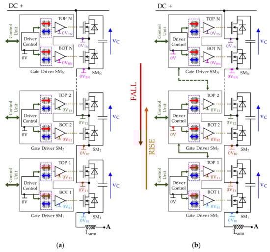
Figure 6.
MMC with regular architecture (a) & MMC with Distributed Galvanic Isolation (DGI) (b).
In order to reduce the galvanic insulation voltage requirements, and allow true modularity of the gate driver structure, the proposed work presents a new approach to distributing the galvanic insulation between each MMC arm gate driver. The structure, called Distributed Galvanic Insulation (DGI), is illustrated in Figure 6b. Only the lowest driver D1 is directly linked to the control unit, its primary being referenced to the safe black reference. Then, D2′s primary reference is connected to D1′s TOP side reference. Similarly, D3′s primary reference is connected to D2′s TOP side reference, until we reach the highest driver, DN, at the top of the architecture. The gate drivers are cascaded and a driver Dp shares the reference of its lower index neighbors D(p−1)’s TOP channel.
Two new important properties then appear:
- Firstly, apart from D1, each driver’s primary shares the same reference as its BOT secondary channel. The voltage across the BOT galvanic insulation is zero;
- Secondly, the voltage between a driver’s primary and its TOP secondary channel is equal to VSM, i.e., 0 V or VC, the capacitor voltage. During normal operations, VC is given in (1) [34]:
VC = UDC/N
The voltages across a submodule gate drivers’ galvanic isolation barriers p for both the regular MMC (a) and the DGI-MMC (b) are given in Figure 7. The middle point of an MMC DC bus is often referenced to Earth. It is thus the same reference as all drivers’ primaries. In the example presented in Figure 7, all submodules from p + 1 to N are bypassed. In that case, the voltage reference 0VTp is directly connected at the DC bus positive pole. The voltage across the galvanic isolation between TOP and primary is thus UDC/2. It is the same voltage between BOT and primary if T2 is ON, and UDC/2 − VC otherwise. With DGI-MMC, as the primary gate driver p is referenced to 0 VBp, the voltage across the galvanic insulation between TOP and primary is VC or 0 V, if T2 is conducting. It is always 0 V between BOT and primary. The isolation voltage requirements are decreased by a factor of N/2 between the primary and TOP side compared to regular MMC according to (1). In most regular MMC, gate drivers are powered with auxiliary power supplies (APS). Many applications draw power from the capacitor submodule. As stated in [35], this becomes very difficult for several hundreds of kilovolt converters. The higher the insulation voltage, the larger and more expensive the magnetic components. The magnetic galvanic insulation requirements would be too bulky and costly. An external power supply is required, again increasing converter cost and volume. With this proposed structure, drawing power from the submodule capacitor is straightforward as each gate driver’s primary side is referenced to its submodule capacitor. The clearance between each side is greatly reduced, which allows for more compact designs. The reduced voltage across galvanic insulations thus highly simplifies the submodule’s gate driver’s design. Another major asset of the structure is the low number of communication wires between the control unit and the power stage. Let’s assume that Nwire is the number of wires between one driver’s submodule and the main control unit. For a three phase MMC with regular architecture, the overall number of wires Nwire_tot is then:
Nwire_tot = 6 N Nwire
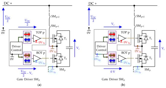
Figure 7.
Voltage across a submodule gate drivers’ galvanic isolation barriers p for regular MMC (a) and DGI-MMC (b).
As N can reach several hundred on very high power applications, the control unit may have trouble managing such a high number of I/O, especially with centralized control schemes. Whereas the MMC-DGI requires only an Nwire data wire per arm, connected to D1, thus, a total of only 6 Nwire for a three-phase MMC. This is a reduction by a factor N and the number of wires is independent of the number of submodules, increasing the converter modularity. Increasing the number of submodules in each arm does not increase the number of wires between the control unit and the converter. This cascaded gate driver structure can be applied to any cascaded converter. It allows the use of classical medium voltage built-in smart gate drivers regardless of the voltage levels of the application. This is a clear improvement in terms of converter cost, volume, and modularity. Furthermore, small built-in gate drivers require little maintenance and are easy to replace. One last asset of the topology is the reduced ElectroMagnetic Interferences (EMI) in the drivers, mainly due to the common-mode currents generated by electromagnetic coupling between the switched power lines and a grounded device [36]. That current flows back to the drivers’ primary sides, usually referenced to ground. This may cause disturbances in the driver electronics (loss of signal integrity, ground bounce…), which may compromise its safe operations. The general idea to limit the impact of common mode currents is usually to increase the impedance between the two drivers’ sides [37]. As the galvanic insulations of the drivers are connected in series in the proposed cascaded structure, the equivalent capacitance in the current path to ground is naturally decreased. The current path in such cascaded structures and its benefits had already been highlighted and described in [38,39]. However, the proposed gate driver structure is different from previous references. In [38,39], gate power supplies are cascaded and the voltage insulation is not decreased. In that paper, communication links and voltage references are cascaded, which highly decreases the gate driver’s voltage insulations. The introduction of smart-gate drivers naturally increases the power modules’ reliability due to their advanced monitoring, diagnosis and protection features. This is a critical point in multilevel structures where the number of power modules is high. In the case of a power module failure, smart gate drivers are able to protect the submodule. Detailed diagnosis can be sent to the main controller through the proposed communication structure.
In the case of a submodule p or a gate driver p failure, the series communication channel can be threatened. To overcome that issue, a “bypass” mechanism can be introduced for online reconfiguration of the gate driver chain. The TOP channel of gate driver p − 1 cannot be directly linked to the primary of gate driver p + 1, due to different voltage references. That redundant link must then be isolated with the same galvanic insulation barrier as the gate drivers themselves. As already stated, the small voltage VC across that galvanic insulation allows for the simple integration of such a communication link. The same redundant mechanisms can be used for the gate driver APS.
The main issue of the DGI-based MMC is the missing connections between the N − 1 drivers and the control unit in each arm. The only available communication channel is the driver chain itself. With smart gate drivers, messages can be exchanged between the members of the chain in both directions and complex procedures can be executed. However, this communication channel suffers delays. A message sent by one driver to another needs to cross the galvanic isolation barrier between the primary and TOP side. That process takes a short time, especially with magnetic components [40], and depends on the availability and the bit rate of the driver communication technology. The time between the sending of one bit by a driver Dp and its reception by the next driver D(p+1) is tdriver. A message sent by D1 is received by DN after crossing N − 1 isolation barriers. For instance, with one hundred SM, and an estimated propagation time tdriver of 100 ns per driver [40], the average time for one bit to cross the whole driver chain is 9.9 µs. Such important delays between the control unit and the drivers must be taken into account when designing the converter. Communication protocols must be designed to limit the number of bits exchanged between the drivers.
In the first part of that work, the Distributed Galvanic Insulation for the MMC had been introduced and studied. Its numerous advantages had been exposed. In the following, a voltage balancing algorithm directly executed by the chained gate drivers is proposed. It will be validated by simulation later in that work. The new communication channel between the drivers and the main controller allows the gate drivers to be part of the converter control. That paper only explores a voltage balancing algorithm. The gate driver structure proposed in that work offers many other possibilities in terms of control, monitoring, and power modules’ reliability that will be thoroughly studied in future works.
3. A Voltage Balancing Algorithm for the DGI-Based MMC
3.1. Description of the Algorithm
Due to the high number of capacitors connected in series, the voltage balancing of multilevel topologies remains a challenge [41]. The so-called voltage balancing algorithm was originally proposed in [1] in order to relieve the main control unit. It is usually executed by fast and dedicated hardware (typically an FPGA), which is added between the main control output and the actual gate signals of the converter switches, as in Figure 2. The modulation stage output is the number of submodules to insert per arm i and per phase j, referred to as the insertion index ni,j. The VBA is then in charge of selecting the right submodules to insert in each arm. The main algorithm idea is based on the measurement or estimation of the arm current and the sorting of all submodule capacitor voltages. Inserted capacitors are charged up by the arm current Ii,j if it is positive and discharged if the arm current is negative. Then, the ni,j capacitor inserted in the arm has the highest voltages if Ii,j is negative and the ni,j capacitor inserted in the arm has the lowest voltages if Ii,j is positive. Although highly reducing the computational burden on the main controller, an external voltage balancing algorithm has the general drawback of increasing the switching frequency, which may increase losses [42]. Various voltage balancing algorithms had been proposed in the literature to answer those issues. HVDC-MMC can have a large number of submodules which highly complicates the practical implementation of such algorithms. High galvanic insulation barriers are required, which reduce communication capabilities, and a high number of communication links are required between the power modules and the control stage. The practical implementation of external voltage balancing algorithms is challenging with the conventional structure (Figure 6a).
The proposed decentralized VBA had already been described in [43]. It shares the structure of the algorithm proposed in [44] that could be referred to as RSF (Reduced Switching Frequency Voltage Balancing Algorithm). Unlike the other external VBA, RSF does not increase the number of switchings from the control stage. That algorithm exhibits the lowest possible switching frequency, at the price of a less efficient balancing. The current number of submodules inserted in the arm i of phase j is ni,j_OLD. The instantaneous difference between the previous insertion indices and the new one, ni,j, is ∆ni,j.
Its absolute value |∆ni,j| is the number of submodules to be switched, and its sign indicates whether submodules must be inserted (positive) or bypassed (negative). RSF’s flowchart is presented in Figure 8. In the following, the function Sign(X) is used which outputs 1 if X ≥ 0, and −1 otherwise. The gate signals are maintained constant while |∆ni,j| = 0. Furthermore, only the bypassed SM can be inserted, while only the inserted SM can be bypassed. That ensures that the number of switchings is exactly |∆ni,j|. With RSF, the converter switching frequency is imposed by the main control unit only. It is a simple and efficient VBA that is easy to implement. Likewise, the proposed algorithm is executed at each change of |∆ni,j|. It is based on the local measurement by each driver of its own capacitor voltage VC. The use of gate drivers able to locally measure the arm current Ii,j [45] is convenient but not mandatory. The algorithm is executed by fast electronics on the primary side. Typically, smart gate drivers equipped with FPGA, like in [25], are perfectly suited for such an application. The overall control structure of the converter is modified, as depicted in Figure 9.

Figure 8.
Flowchart of the Reduced Switching Frequency Voltage Balancing Algorithm [38].
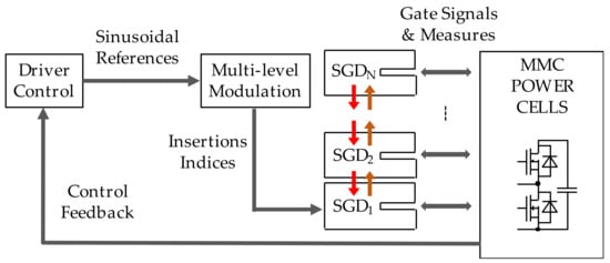
Figure 9.
Control structure of the MMC-DGI with the proposed embedded VBA.
The insertion index is sent directly to the first driver of the chain, D1. No additional control hardware is required between the main controller and the Smart Gate Drivers chain. The channel between the drivers can be used in both directions at the same time (full-duplex). Messages sent from the lower index driver Dp to the higher index driver Dp+1 are said to be “rising”, and are depicted in orange. Messages sent from the higher index driver Dp to the lower index driver Dp+1 are said to be “falling”, and are depicted in scarlet (Figure 6). One phase of the MMC with the proposed Distributed Galvanic Isolation and Voltage Balancing Algorithm is seen in Figure 10. The algorithm only executes one switching at a time. The aim of the decentralized VBA is to find the highest or lowest capacitor voltage among the arm and to switch the corresponding SM state. If ∆ni,j ≠ 0, the algorithm is executed consecutively |∆ni,j| times.
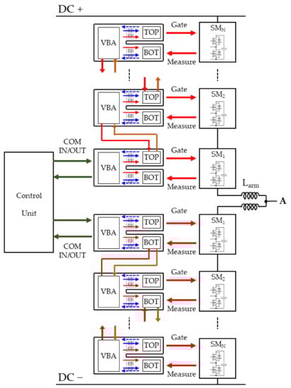
Figure 10.
One MMC-DGI phase with the proposed embedded Voltage Balancing Algorithm.
The selection process is based on simultaneous timing comparisons. Each driver runs two internal counters. One has a duration of tCOUNT, which depends on the submodule priority to switch (which itself depends on the capacitor voltage VC, and RSF rules). The longer the counter, the higher the priority to switch. The second has a fixed duration of tALGO. During the procedure, a token is exchanged between the drivers, depending on their counter durations tCOUNT_P. At the end of the second counter of duration tALGO, the procedure ends, and the driver which owns the token switches its state. The generation of tCOUNT_P and tALGO_P of a driver p is detailed in [43], and recalled in (3) and (4):
where VMAX and VMIN is the maximum and minimum capacitor voltage in normal operations, respectively. In most cases, the capacitor voltage is kept between ±10% of its reference voltage, VCREF. The counter is incremented by q of each clock cycle, of frequency fCLK. The parameter q allows a tradeoff between the sorting accuracy and the algorithm duration. While the value tCOUNT_P depends on the submodule capacitor voltage, tALGO_P is fixed and pre-implemented in the FPGA. During the procedure, N − 1 drivers will be removed from the selection process. They enter a state referred to as sleep mode. When in sleep mode, a driver cannot hold the token and will act as a member of the communication chain, propagating messages, but never interacts with the other gate drivers. A working example illustrates the proposed decentralized algorithm with four cascaded gate drivers.
tCOUNT_P = (VMAX − VCP)/(q fCLK) if Sign(∆ni,j) ≠ Sign(Ii,j)
tCOUNT_P = (VCP − VMIN)/(q fCLK) otherwise
tCOUNT_P = (VCP − VMIN)/(q fCLK) otherwise
tALGO_P = 2 N tDRIVER + (VMAX − VMIN)/(q fCLK) − (p − 1) tDRIVER
There is no specific communication protocol for the proposed algorithm. Only simple bit exchanges are performed in the baseband. No information, like voltage, is sent between drivers, thus no complex communication frames are necessary. As already stated, this is due to the delay inferred by the crossing of galvanic insulations. It is important to maintain at low the number of bits exchanged between the driver. The proposed algorithm highly limits the bit exchange. The impact of the delay on the converter behavior is thoroughly studied through a Matlab/Simscape simulation in the next section.
3.2. Algorithm Working Example
Figure 11a schematizes the four smart gate drivers executing the proposed decentralized algorithm, with “rising” messages depicted in orange and “falling” messages in scarlet. The internal counters of duration tCOUNT_P are represented in blue. The state of the submodule p is given by the variable Sp which is equal to 1, if the submodule is inserted, and −1 otherwise. The corresponding chronograms are given in Figure 11b. According to RSF, the submodule to insert is the one with the highest capacitor voltage value. The chronograms show the frames exchanged between the drivers and their internal counters. The duration of each bit is tdriver. The procedure is divided into 3 steps:
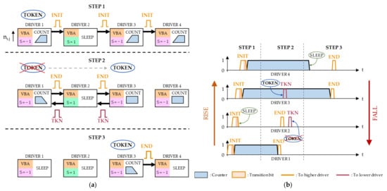
Figure 11.
Typical VBA sequence example divided into 3 steps (a) and corresponding chronogram (b).
Step 1 is the initialization step. As soon as D1 detects a change in the insertion index, the initialization frame is sent to D2. In the example, a submodule must be inserted (|∆ni,j| > 0) and the arm current is negative (Ii,j < 0). In the example, the initialization frame is only constituted of two bits, one for the “start” and the second indicates the sign of ∆ni,j. That second bit is referred to as the transition bit (Figure 11b) which is 1 in the example (submodule insertion). Regardless of the drivers’ states, the initialization frame is instantly propagated along the chain. The algorithm is supposedly executed by FPGA-like devices, which allows the simultaneous sending and receiving of messages. Thus, only a delay of a one-bit duration appears between each driver’s chronogram, regardless of the number of bits of the initialization frame. If the drivers have no access to a local measurement of the arm current sign, an additional bit can be added to the initialization frame for each driver to get the arm current sign. Following the reception of the transition bit, D2 enters sleep mode as it is already inserted. It does not participate in the selection process but propagates the incoming messages. All the other bypassed drivers start their internal counters of durations tCOUNT_P and tALGO_P. D1 takes the token first as it is the first driver to launch its counter.
Step 2 illustrates a token exchange. D1 holds the token and its counter ends. It sends an END bit which rises along the driver chain. D2 propagates it to the first non-sleeping driver, here D3. As D3 is still counting at the reception of that END bit, D3 takes the token (Figure 11b). A TOKEN (TKN) bit is sent back by D3 for D1 to release its token. The TKN bit falls through the chain and D1 loses its token after the reception of that bit and enters sleep mode. All the drivers before D3 have now entered sleep mode. The token exchange step can be repeated several times during the procedure until the token reaches the driver with the longest counter duration, here D3.
Step 3 is the final step of the proposed algorithm. D3 has the longest counter-duration. Indeed, D4′s counter ends before D3′s counter (Figure 11b). As D4 does not have the token, no END bit is sent to D3. D4 enters sleep mode. When D3′s counter ends, it sends a rising END bit like in the previous step. However, this time, as all the upper drivers are already in sleep mode, it gets no TKN bit back. That way, its token is not erased.
The procedure ends when the second internal counter of duration tALGO_P ends. D3 switches its state at the end of that counter and all drivers exit sleep mode to be ready for another cycle. The end of the procedure is synchronous for all drivers. It can be seen in Figure 11b that D4 shares the same code as other drivers for convenience and modularity of the structure but its output is simply not connected. The proposed algorithm is a succession of one initialization phase followed by several token exchanges and a final step. As all the counters are running at the same time, there is no need to compare all the voltages together. Only the “token bearer” can access the communication channels, avoiding loss of information and ensuring the process of stability. The token can never be lost, nor can it be multiplied. Furthermore, the delays introduced by the barriers don’t cause synchronization issues between drivers, as they are automatically and naturally counterbalanced. Even if all the drivers have different barriers’ delays (different tdriver) the synchronization won’t be impacted.
3.3. Algorithm Flowchart
The procedure can be easily implemented using a set of few internal flags. They characterize the state of the driver:
- VBA: The selection procedure is currently being executed. Set to 1 after the reception of the initialization frame and maintained during the overall procedure (reset after tALGO_p);
- COUNT: The driver is counting. Set to 1 when the driver starts counting and reset after tCOUNT_p;
- SLEEP: The driver is in sleep mode. Set to 1 when the driver enters sleep mode and reset at the end of the procedure;
- TOKEN: The driver carries the token. Set to 1 when the driver gets the token and reset when the token is given to another driver (Step 2) or at the end of the procedure (Step 3, in which case the driver switches its state);
Furthermore, only 3 different communication frames will be exchanged during the procedure. They have already been introduced in the previous example:
- Initialization frame (INIT): The initialization frame is generated by D1 when an event of ∆ni,j ≠ 0 is detected. It is rising along the whole chain to DN. It begins with a specific code for the VBA procedure, which was only one bit long in the previous example. It also contains the information required for the counter generation (sign(∆ni,j) and sign(Ii,j) if necessary);
- END bit: A rising bit sent by a driver which holds the token when COUNT is reset;
- TOKEN bit (TKN): A falling bit sent by a driver which receives an END bit when COUNT is not reset.
Only simple Boolean tests are performed during the procedure. The algorithm can be described by three concurring flowcharts, as shown in Figure 12. The main one, in charge of the counters’ generation, is presented in Figure 12a. It is only active when VBA is true. The two smaller flowcharts in Figure 12 b,c show the procedures executed when a bit is received from a lower index driver (rising bit) and from a higher index driver (falling bit) respectively. Those two flowcharts are always active. FPGAs are typically designed to handle such parallel tasks. The proposed decentralized algorithm can be schematized as in Figure 13. The Boolean tests Crit. 1 and Crit. 2 have been detailed in [43]. They are given in (5) and (6) respectively:
Si ≠ Sign(∆ni,j)
Sign(∆ni,j) ≠ Sign(Ii,j)
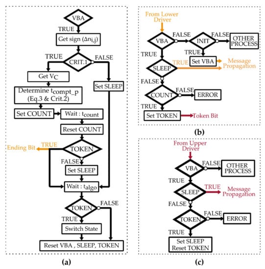
Figure 12.
Three concurring flowcharts of the proposed voltage balancing algorithm: main (a), rising bit reception (b), falling bit reception (c).
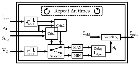
Figure 13.
Equivalent functional bloc of the proposed embedded algorithm.
At the reception of the initialization frame, each of the drivers checked for Crit. 1 and Crit. 2. Crit. 1 avoids submodules that are already inserted to be part of the procedure when submodule insertion is required and reciprocally avoids submodules that are already bypassed to be part of the procedure when submodule bypassing is required. If Crit. 1 is false, the driver enters sleep mode. Crit. 2 is used for the generation of tCOUNT_P in (3). If Crit. 2 is true, the lowest capacitor voltage needs to be switched. Otherwise, it is the highest capacitor voltage that needs to be switched.
To our knowledge, that work is the first to propose a voltage balancing algorithm directly executed by a gate driver chain apart from our previous introduction to that work in [43]. It is made possible thanks to the introduction of SGD in MMC with Distributed Galvanic Insulation. MMC decentralized control schemes in the literature use external slave controllers. The innovative solution proposed in that work does not require any additional external hardware. The proposed algorithm answers the need of external voltage balancing algorithm, using CPLD/FPGA technology often embedded on SGD. In the next section, an accurate simulation tool is developed in order to validate the algorithm’s behavior.
4. Simulation of the Proposed Gate Driver Embedded Algorithm
4.1. Simulation set-up
A simulation model of a three-phase grid-tied MMC inverter is built on Matlab/Simscape software. The power stage is realized using Simscape power building blocks, allowing a highly accurate, easily scalable, and reliable model of the converter. The converter model is built with passive and active elements with a Simscape library as in Figure 1. The aim of the following simulations is to demonstrate that smart gate drivers can be part of a high-power MMC control and the feasibility of the proposed decentralized voltage balancing algorithm implementation. The gate drivers and the main controller are realized with conventional Simulink building blocks. The simple logic functions executed during the VBA are implemented with logical and relational operators, switches and flip-flops and no Matlab code is executed. Such design using elementary building blocks typically mimics the internal behavior of FPGA-like devices. A unique VBA-embedded gate-driver model is realized, which is then used for all drivers of each 6 converter arms. Only Driver 1 has a slightly different architecture due to the interface between its primary side and the converter main control unit. That low level of model is chosen to accurately represent a CPLD/FPGA device, in order to demonstrate the practical implementation of such algorithms on a real SGD [25].
Each driver is linked to its two closest neighbors via two communication lines, for rising and falling messages respectively. Drivers can gain access to the measurement of its submodule capacitor voltage and the arm current locally through Zero Order Hold (ZOH). Due to its particular topology, the MMC requires specific controls. Indeed, not only the AC output current must be regulated but also the so-called “circulating current” in the converter. The AC current is flowing from both DC poles to the AC side through the converter arms. The useful current is thus a common-mode current from the DC side. Differential mode current, often called circulating current, is not flowing on the AC side. The circulating current is generated by the instantaneous power exchanges between the arm capacitors and the AC side, which mostly generates a 2nd order harmonic [9]. The differential voltage across the inductor (VD,i,j on) must be controlled in order to limit the capacitor voltage deviation and increase the converter efficiency. For that reason, most of MMC control structures feature an arm current controller, divided in two parts. Indeed, the output current and the circulating current can be controlled independently. Details about the MMC internal dynamics and control are not further given in this work. A schematic of the grid-tied inverter with the input and output control quantities is given in Figure 14. The control laws selected for that converter simulation are based on vector control due to their simplicity and great efficiency. Typical (P,Q) control in Park frame is chosen for the output controller. The converter control schemes are given in the next figures. Its overall schematic is given in Figure 15.
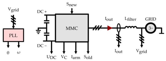
Figure 14.
Grid-tied MMC input and output control quantities.
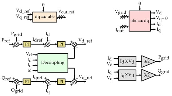
Figure 15.
Output power control schematic of the proposed inverter with (P,Q) grid regulation in a typical park frame.
The circulating current controller is based on the work proposed in [44,46]. The main control scheme is named “Circulating Current Suppression Control (CCSC)” and is based on vector control to suppress the parasitic 2nd order harmonic of the circulating current. In [46], an improvement of the CCSC had been proposed. The regulation of the zero-sequence circulating current icirc_0 is added, which was originally left uncontrolled in [44]. A DC component must circulate in the converter phases in order to ensure the power transfer between the DC and the AC sides. Neglecting the converter and filter losses, the following equations can be written as in (7):
PDC=PAC
IDC=PAC/(3UDC)
IDC=PAC/(3UDC)
If the circulating current DC component is left uncontrolled, instantaneous power unbalances may appear between the DC and the AC sides. This would lead to MMC capacitor stored energy variations, threatening stability. The control scheme proposed in [46] uses two cascaded PI controllers. The outer loop is the energy controller whose output feeds up the zero-sequence circulating current controller. The circulating current controller schematic is given in Figure 16. The total converter leg energy EΣjis calculated as in Figure 16. Finally, the overall control structure of the proposed grid-tied inverter is given in Figure 17. Vdiff_ref and Vout_ref are, respectively, the outputs of the circulating current controller and the grid power controller. The arm voltage references Uu,j_ref and Ul,j_ref of phase j are generated with the following equations:
Uu,j_ref = Vdiff_ref − Vout_ref + UDC/2
Ul,j_ref = Vdiff_ref + Vout_ref + UDC/2
Ul,j_ref = Vdiff_ref + Vout_ref + UDC/2
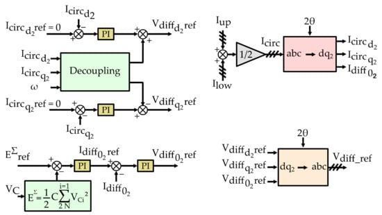
Figure 16.
Circulating Current Suppression Control (CCSC) schematic [46].
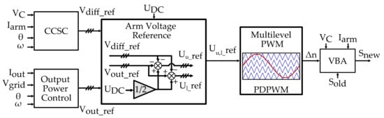
Figure 17.
Overall control chain of the proposed simulated Modular Multilevel Converter.
The modulation scheme used in that simulation is the classical Phase-Displacement Pulse Width Modulation (PDPWM). The output of the modulation stage is the insertion transition index ∆ni,j which is directly fed to the chained gate drivers of each arm, symbolized by the “VBA” bloc (Figure 13). The converter and drivers’ parameters, as well as the power conditions on both DC and AC sides of the first simulation run, are summed up in Table 1.

Table 1.
Grid-tied MMC inverter parameters.
4.2. Working Example with N = 15
A simulated working example is proposed with 15 submodules for better readability where the arm current is positive and |Δni,j| = 1 at t = 0 s. The 15 corresponding chronograms are given in Figure 18. The different rising and falling bits, and the internal counters in each driver, can be observed as in Figure 11b. The state of SM14 is also depicted and the voltages of each capacitor are indicated. The lowest capacitor voltage among the bypassed capacitors needs to be switched on, according to RSF. Five submodules are already inserted: SM3, SM7, SM8, SM13 and SM15. In the example, Vmax, Vmin, tdriver and q are selected as in Table 1. The value of talgo is calculated as in (4) with N = 15:
talgo = 16.7 µs
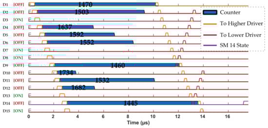
Figure 18.
Fifteen gate drivers’ chronograms during the proposed procedure.
At t = 0 s, the insertion query is received by Driver 1 and the initialization frame is sent through the chain. The submodules already inserted in the arm don’t generate counters and enter sleep mode. In the example, the token is first given to D1, then D9 takes the token, and, finally, D14 is the last token bearer. The simulated behavior of the gate drivers matches the previous working examples. D14 switches its state, 16.7 µs (talgo), after the reception of the INIT frame.
4.3. Grid-Tied MMC Steady-State Simulation
A first simulation of the grid-tied MMC inverter is realized in steady-state. The converter’s three phases output currents and voltages are depicted in Figure 19. The output voltages are not filtered yet they are very close to a sinusoidal waveform. This is a significant advantage of multilevel topologies. The output currents are smoothed by the inductor Lfilter and their maximum value is close to IMAX = 335 A. The apparent power fed to the grid is given in (10):
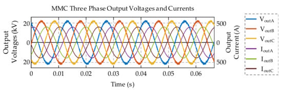
Figure 19.
MMC three phases output voltages and currents with proposed embedded algorithm.
The output power is well regulated and the proposed algorithm does not impact the output waveforms. The converter legs’ circulating currents are depicted in Figure 20 in both (A,B,C) and (d2,q2,02) frames. It can be seen that the 2nd order harmonic is clearly suppressed from the three-phase system. The d and q components of the circulating current are maintained around 0 A. The circulating currents and the phase energy sum are well regulated by the converter control scheme.
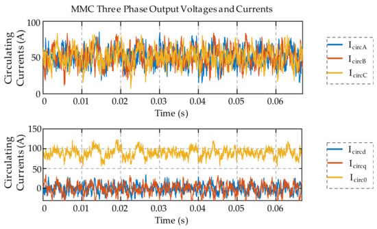
Figure 20.
MMC three phases circulating currents with proposed embedded algorithm in (A,B,C) frame (Up) and (d2,q2,02) frame (Down).
The 60 capacitor voltages of the A-phase are presented on the left of Figure 21. It can be seen that they are kept in the range of VSM_Ref ± 10% (dash-dotted lines). Furthermore, the proposed algorithm allows the effective balance of the capacitor voltages among each arm. In order to compare the proposed algorithm with RSF, another simulation is performed under the exact same power conditions but the chained drivers are replaced by a perfect RSF algorithm. This algorithm does not infer delays between the modulation stage and the power stage. The 60 capacitor voltages of phase A generated with RSF are presented on the right of Figure 21. It can be seen that the waveforms generated by the proposed method and RSF’s are very similar, which validates the good performance of the embedded voltage balancing algorithm.
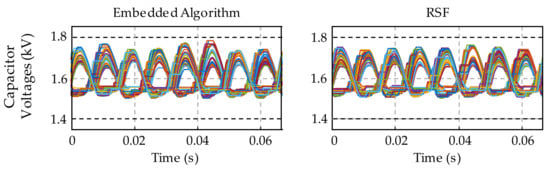
Figure 21.
MMC A-phase Capacitor voltages waveform comparison: Embedded Algorithm (left), RSF (right).
Finally, the dynamic behavior of the proposed algorithm is studied in Figure 22. The A-phase upper arm expected insertion index (ni,j, output of the modulation stage) is compared to the effective insertion index (Snew, output of the proposed algorithm). As expected, a constant delay of tALGO is observed between the two quantities. Due to its particular structure, any output of the proposed algorithm is maintained for a minimum duration of tALGO. However, due to the PWM characteristics of the insertion index, very narrow reference pulses can be produced with durations shorter than tALGO. In that case, the insertion index reference is distorted at the output of the proposed VBA, as circled in Figure 22.
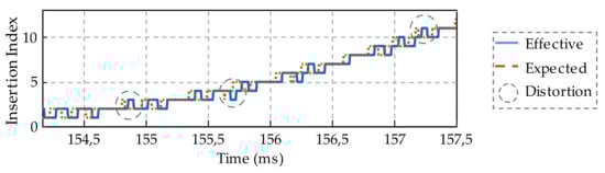
Figure 22.
MMC A-phase Insertion index: expected vs. effective.
4.4. Grid-Tied MMC Dynamic Simulation
For this test, the apparent power reference is initially set to SAC = 7 MVA, with a power factor of cos(φ) = 0.707. At t = 0, a brutal load impact is simulated by reducing the maximum grid voltage from 20 kV to 13.5 kV (67.5%). The power reference is maintained as constant during the grid voltage step. The output voltages and currents are depicted in Figure 23 (Up), together with the measured active and reactive grid powers and their references (Middle). It can be seen that the converter exhibits a fast dynamic and the output power is efficiently regulated less than 10 ms after the load impact. The converter remains stable under load transients. This can be demonstrated in Figure 23 (Bottom), where the A-phase 60 capacitor voltages are depicted. They are kept in the range of VSM_Ref ± 10% and naturally equilibrate after the output power transients. The arm capacitor voltages’ equilibrium is not threatened by the load impact. The expected and effective insertion indices are compared in Figure 24. During fast transients, the effective insertion index is delayed compared to the expected insertion index. That delay can accumulate under very stiff transients (|Δni,j| ≫ 1). The algorithm dynamics can be assimilated to a slew rate, which value dΔni,j/dt is defined by talgo as in(11):
dΔni,j/dt = 1/talgo
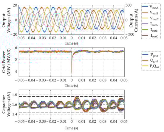
Figure 23.
Simulation results under load impact: three-phase output voltages and currents (Up), power fed to the AC grid (Middle), and A-phase 60 capacitor voltages (Down).
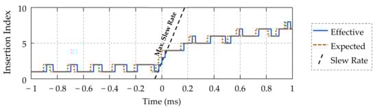
Figure 24.
MMC A-phase Insertion index: expected vs. effective under load impact.
The control dynamic parameters must be selected in accordance with the algorithm dynamics. With sufficiently high switching frequency and reasonably fast control dynamics, which is the case in many AC grid applications, the value of |Δni,j| can be kept low, as in Figure 24. This ensures the stability of the MMC-DGI converter.
Previous simulations allowed to demonstrate the efficiency of the proposed decentralized algorithm for the MMC. It exhibits the same behavior as RSF in steady-state. Its particular dynamics makes the converter response time not as fast as with conventional algorithms. However, it had been shown that the MMC exhibits great stability, even after load impacts, without compromising the converter safety. The output voltages, currents and power are not impacted by the proposed algorithm delay. The circulating currents follow the references. The study of the insertion index allows us to highlight a small distortion effect caused by the SGD chain delays. However, narrow pulses are inherent to PWM techniques [47]. Modulations like Nearest Level control avoid such issues. The constant slew rate implied by the proposed algorithm had also been studied. This must be taken into account during MMC design to adjust the control dynamic parameters. It has been shown that this slew rate has little impact on the converter’s ability to regulate its output power, even during sharp grid voltage changes.
5. Discussion
The work has introduced a novel cascaded gate driver architecture for multilevel converters. It offers numerous advantages compared to the conventional gate driver structure. The voltage across the gate drivers’ galvanic insulation becomes independent of the application voltage and is reduced to the submodule capacitor voltage. This relatively low level of voltage insulation allows the use of built-in ready-to-plug gate drivers. With a conventional MMC structure, the voltage across the gate drivers’ galvanic isolations is at least equal to the converter DC voltage. Increasing the converter voltage levels implies a design of all gate driver’ galvanic insulations again. The converter modularity is thus highly increased with the Distributed Galvanic Insulation. Indeed, the number of data and power wires between the main control unit and the converter is independent of the number of submodules. The DC voltage and the number of submodules can be arbitrarily increased as the gate driver isolation voltage only depends on the submodule capacitor voltage. Furthermore, the converter cost and volume are reduced due to much lower requirements for the isolation magnetic component and the reduced number of wires. The introduction of intelligent gate drivers in the MMC is unlocked thanks to the proposed structure. The assets of smart gate drivers have already been highlighted in the literature. They feature various power bridge protections such as short circuits or crosstalk suppression. SGD can also allow the reduction of switching losses (between 30% and 60% according to literature) and power module condition monitoring. Furthermore, they can be equipped with bidirectional communication channels and programmable logical components (CPLD or FPGA). These are critical improvements for MMC efficiency, reliability and safety.
In return, the communication link between the drivers and the main control unit is weakened. New bidirectional communication channels must be introduced to ensure communication between the main control units and the arm gate drivers. Such communication features can be of various types (optic fiber, planar transformers, …) and allow gate drivers to take part in the converter control. Typically, smart gate drivers are equipped with fast and programmable logic components, like FPGAs. Such drivers are perfectly suited for the proposed Distributed Galvanic Insulation. They allow fast and bidirectional communications between the drivers while being able to execute complex algorithms [25]. The messages are cascaded through each SGD one by one. With few redundancies, the proposed control structure ensures converter safe operation even in the case of a submodule or gate driver failure. Classical decentralized control and external voltage balancing algorithms cannot be directly applied to the proposed structure as the gate driver’s primaries do not share the same voltage reference anymore. With the MMC-DGI, new control methods must be found, particularly for the balance of the arm capacitor voltages. The work introduced an innovative voltage balancing algorithm which was directly executed by the chained gate drivers. Each of them runs a simple piece of code, which allows us to decentralize the MMC voltage balancing algorithm and involves the gate drivers in the converter control relieving the main controller. The simplicity of the proposed solution is one of its main advantages. Any driver able to communicate with its close environment can execute the algorithm as only few Boolean tests, bits exchanges and counters generation are required. This can be easily realized using elementary analog circuits with a small number of logical gates, or standard FPGA. The structure of the algorithm is the same as RSF. It features a fixed and controlled execution time and a tunable resolution parameter q. With that parameter, a trade-off can be found between the execution time and the accuracy of the sorting, depending on the application. Furthermore, the embedded algorithm does not restrain the modularity of the structure. Increasing the number of submodules will also increase the algorithm execution time but not its complexity or structure. The same algorithm is executed by all the drivers, regardless of the number of submodule N in the chain. In the case of changing N, only the new value of talgo needs to be changed. That value can, for instance, be sent along the driver channel of the converter startup, avoiding manual reprogramming of each gate driver. An efficient simulation tool had been built on Matlab/Simscape software. The proposed VBA is implemented using logic blocks that mimic fast analog circuit behavior. The simulation allowed us to verify the ability of the algorithm to balance the capacitor voltages of a three-phase grid-tied MMC with 30 submodules per arms. A first test had shown that the proposed algorithm mimics RSF’s behavior and doesn’t disturb converter control. A second test allowed us to study the dynamic response of the algorithm. It had been shown that the converter stays stable even under load impacts.
Future works will focus on the very promising DGI structure and its novel control schemes. The Matlab/Simscape simulation tool with logical blocks allowed a conceptual validation of the proposed algorithm. The next step of the work will be the implementation of the proposed algorithm on real physical systems. A smart gate driver chain equipped with FPGAs for MMC submodules is currently being built. The simulation model is structurally built using logic blocks and its proposed algorithm implementation in HDL language is thus straightforward. Integrating smart gate drivers in HVDC structures will potentially unlock new converter designs, where the gate drivers have a central role in the converter control. Further studies may also allow improvements of the current algorithm and the DGI itself.
Author Contributions
Conceptualization, J.-C.O., C.D. and N.G.; methodology, C.D., J.-C.O., N.G. and F.P.; software, C.D.; validation, C.D., J.-C.O., N.G. and F.P.; formal analysis, C.D.; investigation, C.D.; writing—original draft preparation C.D.; writing—review and editing, J.-C.O., N.G., F.P. and C.B.; visualization, C.D.; supervision, J.-C.O., N.G. and F.P. All authors have read and agreed to the published version of the manuscript.
Funding
This research was funded by the RFI WISE project.
Conflicts of Interest
The authors declare no conflict of interest.
Nomenclature
| N | Number of submodule per arm |
| LARM | Arm inductor |
| UDC | DC bus voltage |
| IDC | DC bus current |
| IuJ,lJ | Upper and lower arm currents of phase j |
| UuJ,lJ | Upper and lower arm voltages of phase j |
| VDuJ,lJ | Upper and lower arm inductor voltages of phase j |
| VSM | Submodule voltage |
| CSM | Submodule capacitor |
| ISM | Submodule current |
| VC | Submodule capacitor voltage |
| VDSON | Power MOSFET Drain-Source voltage |
| NWIRE | Number of connection wires between one submodule gate driver and main control unit |
| NWIRE_TOT | Number of connection wires between all converter gate drivers and main control unit |
| tdriver | Time between the sending of one data bit by a driver and its reception by next driver |
| ni,j | Updated arm insertion index |
| ni,j_OLD | Current arm insertion index |
| Δni,j | Transition insertion index |
| tcount_p | Counter duration of driver p |
| talgo_p | Algorithm duration executed by driver p |
| Vmax | Maximum allowable submodule capacitor voltage |
| Vmin | Minimum allowable submodule capacitor voltage |
| Q | Counter voltage resolution |
| fCLK | Clock frequency |
| Sold | Current arm gate drivers’ signals |
| Snew | Updated arm gate drivers’ signals |
| Icirc_A,B,C | Circulating current in stationary frame (A,B,C) |
| Icirc_d,q,0 | Circulating current in rotating frame (d2,q2,O2) |
| PDC | DC side power |
| PAC | AC side power |
| SAC | Apparent power at the AC side |
| EΣj | Total converter leg energy |
References
- Lesnicar, A.; Marquardt, R. An innovative modular multilevel converter topology suitable for a wide power range. In Proceedings of the 2003 IEEE Bologna Power Tech Conference Proceedings, Bologna, Italy, 23–26 June 2003; Volume 3, pp. 272–277. [Google Scholar] [CrossRef]
- Martinez-Rodrigo, F.; Ramirez, D.; Rey-Boue, A.B.; De Pablo, S.; Herrero-De Lucas, L.C. Modular multilevel converters: Control and applications. Energies 2017, 10, 1709. [Google Scholar] [CrossRef]
- Perez, M.A.; Ceballos, S.; Konstantinou, G.; Pou, J.; Aguilera, R.P. Modular Multilevel Converters: Recent Achievements and Challenges. IEEE Open J. Ind. Electron. Soc. 2021, 2, 224–239. [Google Scholar] [CrossRef]
- Dorn, J.; Gambach, H.; Strauss, J.; Westerweller, T.; Alligan, J. Trans Bay Cable–A Breakthrough of VSC Multilevel Converters in HVDC Transmission. In Proceedings of the Cigré Colloquium, San Francisco, CA, USA, 2–6 March 2012; pp. 1–6. [Google Scholar]
- Siemens SINAMICS PERFECT HARMONY GH180. Available online: https://www.lda-portal.siemens.com/siemlda/en/109764441 (accessed on 21 May 2021).
- Mendonca, D.D.C.; Cupertino, A.F.; Pereira, H.A.; Teodorescu, R. Minimum Cell Operation Control for Power Loss Reduction in MMC-Based STATCOM. IEEE J. Emerg. Sel. Top. Power Electron. 2021, 9, 1938–1950. [Google Scholar] [CrossRef]
- Vijeh, M.; Rezanejad, M.; Samadaei, E.; Bertilsson, K. A General Review of Multilevel Inverters Based on Main Submodules: Structural Point of View. IEEE Trans. Power Electron. 2019, 34, 9479–9502. [Google Scholar] [CrossRef]
- Tian, Y.; Wickramasinghe, H.R.; Li, Z.; Konstantinou, G. Modular Multilevel Converter Sub-modules for HVDC Applications. In Proceedings of the 2020 IEEE 9th International Power Electronics and Motion Control Conference (IPEMC2020-ECCE Asia), Nanjing, China, 29 November–2 December 2020; pp. 1510–1515. [Google Scholar] [CrossRef]
- Lyu, J.; Zhang, X.; Cai, X.; Molinas, M. Harmonic State-Space Based Small-Signal Impedance Modeling of a Modular Multilevel Converter with Consideration of Internal Harmonic Dynamics. IEEE Trans. Power Electron. 2019, 34, 2134–2148. [Google Scholar] [CrossRef]
- Liu, M.; Li, Z.; Yang, X. A universal mathematical model of modular multilevel converter with half-bridge. Energies 2020, 13, 4464. [Google Scholar] [CrossRef]
- Oates, C. Modular multilevel converter design for VSC HVDC applications. IEEE J. Emerg. Sel. Top. Power Electron. 2015, 3, 505–515. [Google Scholar] [CrossRef]
- Hu, P.; He, Z.; Li, S.; Guerrero, J.M. Non-Ideal Proportional Resonant Control for Modular Multilevel Converters under Sub-Module Fault Conditions. IEEE Trans. Energy Convers. 2019, 34, 1741–1750. [Google Scholar] [CrossRef]
- Liu, M.; Li, Z.; Yang, X. Tracking control of modular multilevel converter based on linear matrix inequality without coordinate transformation. Energies 2020, 13, 1978. [Google Scholar] [CrossRef]
- Yang, Q.; Ding, T.; He, H.; Chen, X.; Tao, F.; Zhou, Z.; Xu, Y.; Chen, S. Model predictive control of MMC-UPFC under unbalanced grid conditions. Int. J. Electr. Power Energy Syst. 2020, 117, 105637. [Google Scholar] [CrossRef]
- Seleme, S.I.; Grégoire, L.A.; Cousineau, M.; Ladoux, P. Modular control with carrier auto-interleaving and capacitor-voltage balancing for MMCs. IET Power Electron. 2019, 12, 817–828. [Google Scholar] [CrossRef]
- Xia, B.; Li, Y.; Li, Z.; Konstantinou, G.; Xu, F.; Gao, F.; Wang, P. Decentralized Control Method for Modular Multilevel Converters. IEEE Trans. Power Electron. 2019, 34, 5117–5130. [Google Scholar] [CrossRef]
- Phan, Q.D.; Gateau, G.; Cousineau, M.; Veit, L.; De Milly, R.; Mannes-Hillesheim, M. Ultra-fast decentralized self-aligned carrier principle for multiphase/multilevel converters. In Proceedings of the 2020 IEEE International Conference on Industrial Technology (ICIT), Buenos Aires, Argentina, 26–28 February 2020; pp. 517–522. [Google Scholar] [CrossRef]
- Kadavelugu, A.; Bhattacharya, S. Design considerations and development of gate driver for 15 kV SiC IGBT. In Proceedings of the 2014 IEEE Applied Power Electronics Conference and Exposition—APEC 2014, Fort Worth, TX, USA, 16–20 March 2014; pp. 1494–1501. [Google Scholar] [CrossRef]
- Zhang, L.; Ji, S.; Gu, S.; Huang, X.; Palmer, J.; Giewont, W.; Wang, F.; Tolbert, L.M. Design considerations of high-Voltage-insulated gate drive power supply for 10 kV SiC MOSFET in medium-voltage application. In Proceedings of the 2019 IEEE Applied Power Electronics Conference and Exposition (APEC), Anaheim, CA, USA, 17–21 March 2019; pp. 425–430. [Google Scholar]
- Incorporated, T.I. Automotive Dual-Channel, SiC MOSFET Gate Driver Reference Design With Two-Level Turnoff Protection. Available online: https://www.ti.com/lit/ug/tidue55b/tidue55b.pdf?ts=1612425912769&ref_url=https%253A%252F%252Fwww.google.com%252F (accessed on 10 June 2021).
- PowerIntegration 2SC0635T2A1-45 Preliminary Datasheet. Available online: https://gate-driver.power.com/products/scale-2-driver-cores/2sc0635t/2sc0635t2ax-45/ (accessed on 8 December 2020).
- Bouguet, C.; Ginot, N.; Batard, C. Communicating gate driver for SiC MOSFET. In Proceedings of the International Exhibition and Conference for Power Electronics, Intelligent Motion, Renewable Energy and Energy Management, Nuremberg, Germany, 10–12 May 2016; pp. 712–719. [Google Scholar]
- Bouguet, C.; Ginot, N.; Batard, C. Communication Functions for a Gate Driver under High Voltage and High dv/dt. IEEE Trans. Power Electron. 2018, 33, 6137–6146. [Google Scholar] [CrossRef]
- Tripathi, A.; Mainali, K.; Madhusoodhanan, S.; Yadav, A.; Vechalapu, K.; Bhattacharya, S. A MV intelligent gate driver for 15 kV SiC IGBT and 10 kV SiC MOSFET. In Proceedings of the 2016 IEEE Applied Power Electronics Conference and Exposition (APEC), Long Beach, CA, USA, 20–24 March 2016; pp. 2076–2082. [Google Scholar] [CrossRef]
- Weckbrodt, J.; Ginot, N.; Batard, C.; Le, T.L.; Azzopardi, S. A bidirectional communicating power supply circuit for smart gate driver boards. IEEE Trans. Power Electron. 2020, 35, 8540–8549. [Google Scholar] [CrossRef]
- Jones, G.T.; Siwakoti, Y.P.; Rogers, D.J. Active Gate Drive to Increase the Power Capacity of Hard-Switched IGBTs. IEEE J. Emerg. Sel. Top. Power Electron. 2021, 9, 2247–2257. [Google Scholar] [CrossRef]
- Shu, L.; Zhang, J.; Shao, S. Crosstalk Analysis and Suppression for a Closed-Loop Active IGBT Gate Driver. IEEE J. Emerg. Sel. Top. Power Electron. 2019, 7, 1931–1940. [Google Scholar] [CrossRef]
- Wang, Z.; Shi, X.; Tolbert, L.M.; Wang, F.; Blalock, B.J. A di/dt feedback-based active gate driver for smart switching and fast overcurrent protection of IGBT modules. IEEE Trans. Power Electron. 2014, 29, 3720–3732. [Google Scholar] [CrossRef]
- Shu, L.; Zhang, J.; Peng, F.; Chen, Z. Active Current Source IGBT Gate Drive with Closed-Loop di/dt and dv/dt Control. IEEE Trans. Power Electron. 2017, 32, 3787–3796. [Google Scholar] [CrossRef]
- Ling, Y.; Zhao, Z.; Zhu, Y. A Self-Regulating Gate Driver for high Power IGBT. IEEE Trans. Power Electron. 2021, 36, 3450–3461. [Google Scholar] [CrossRef]
- Miyazaki, K.; Abe, S.; Tsukuda, M.; Omura, I.; Wada, K.; Takamiya, M.; Sakurai, T. General-Purpose Clocked Gate Driver IC With Programmable 63-Level Drivability to Optimize Overshoot and Energy Loss in Switching by a Simulated Annealing Algorithm. IEEE Trans. Ind. Appl. 2017, 53, 2350–2357. [Google Scholar] [CrossRef]
- Weckbrodt, J.; Ginot, N.; Batard, C.; Azzopardi, S. Monitoring of Gate Leakage Current on SiC Power MOSFETs: An Estimation Method for Smart Gate Drivers. IEEE Trans. Power Electron. 2021, 36, 8752–8760. [Google Scholar] [CrossRef]
- Van Der Broeck, C.H.; Polom, T.A.; Lorenz, R.D.; De Doncker, R.W. Real-Time Monitoring of Thermal Response and Life-Time Varying Parameters in Power Modules. IEEE Trans. Ind. Appl. 2020, 56, 5279–5291. [Google Scholar] [CrossRef]
- Sharifabadi, K.; Harnefors, L.; Nee, H.-P.; Norrga, S.; Teodorescu, R. Design, Control and Application of Modular Multilevel Converters for HVDC Transmission Systems; Wiley: Hoboken, NJ, USA; IEEE Press: Piscatway, NJ, USA, 2016; ISBN 978-1-118-85156-2. [Google Scholar]
- Heinig, S.; Jacobs, K.; Ilves, K.; Norrga, S.; Nee, H.-P. Auxiliary Power Supplies for High-Power Converter Submodules: State-of-the-Art and Future Prospects. IEEE Trans. Power Electron. 2020. [Google Scholar]
- Meng, W.; Zhang, F.; Fu, Z.; Dong, G. High dv/dt Noise Modeling and Reduction on Control Circuits of GaN-Based Full Bridge Inverters. IEEE Trans. Power Electron. 2019, 34, 12246–12261. [Google Scholar] [CrossRef]
- Bhattacharya, S. Gate drivers for wide bandgap power devices. In Wide Bandgap Semiconductor Power Devices: Materials, Physics, Design, and Applications; Baliga, B.J., Ed.; Woodhead Publishing: Amsterdam, The Netherlands, 2019; pp. 249–300. ISBN 978-0-08-102306-8. [Google Scholar]
- Nguyen, V.S.; Kerachev, L.; Lefranc, P.; Crebier, J.C. Characterization and Analysis of an Innovative Gate Driver and Power Supplies Architecture for HF Power Devices with High dv/dt. IEEE Trans. Power Electron. 2017, 32, 6079–6090. [Google Scholar] [CrossRef]
- Nguyen, V.S.; Lefranc, P.; Crebier, J.C. Higher switching speed of power devices in series connection achieved by modifying the gate driver architecture. In Proceedings of the 2017 19th European Conference on Power Electronics and Applications (EPE’17 ECCE Europe), Warsaw, Poland, 11–14 September 2017; pp. 1–10. [Google Scholar] [CrossRef]
- Weckbrodt, J.; Ginot, N.; Batard, C.; Azzopardi, S. Short pulse transmission for sic communicating gate driver under high dv/dt. In Proceedings of the International Exhibition and Conference for Power Electronics, Intelligent Motion, Renewable Energy and Energy Management, Nuremberg, Germany, 5–7 June 2018; pp. 1552–1557. [Google Scholar]
- Mahé, A.; Houari, A.; Olivier, J.-C.; Machmoum, M.; Deniaud, J. Modulation Technic Highlight for State of Charge Balancing on a Series Cascaded Converter. Electrimacs 2017, 107–118. [Google Scholar]
- Huang, S.; Liao, W.; Liu, P.; Tang, W.; Huang, S. Analysis and calculation on switching frequency and switching losses of modular multilevel converter with maximum sub-module capacitor voltage deviation. IET Power Electron. 2016, 9, 188–197. [Google Scholar] [CrossRef]
- Corentin, D.; Nicolas, G.; Jean-Christophe, O.; Frederic, P. Modular Multilevel Converter with Distributed Galvanic Isolation: A Decentralized Voltage Balancing Algorithm with Smart Gate Drivers. In Proceedings of the 2020 22nd European Conference on Power Electronics and Applications (EPE’20 ECCE Europe), Lyon, France, 7–11 September 2020; Volume 1, pp. 1–10. [Google Scholar] [CrossRef]
- Tu, Q.; Xu, Z.; Xu, L. Reduced Switching-frequency modulation and circulating current suppression for modular multilevel converters. IEEE Trans. Power Deliv. 2011, 26, 2009–2017. [Google Scholar] [CrossRef]
- Wang, J.; Shen, Z.; Dimarino, C.; Burgos, R.; Boroyevich, D. Gate driver design for 1. In 7kV SiC MOSFET module with Rogowski current sensor for shortcircuit protection. In Proceedings of the 2016 IEEE Applied Power Electronics Conference and Exposition (APEC), Long Beach, CA, USA, 20–24 March 2016; pp. 516–523. [Google Scholar] [CrossRef]
- Freytes, J.; Bergna, G.; Suul, J.A.; D’Arco, S.; Gruson, F.; Colas, F.; Saad, H.; Guillaud, X. Improving Small-Signal Stability of an MMC With CCSC by Control of the Internally Stored Energy. IEEE Trans. Power Deliv. 2018, 33, 429–439. [Google Scholar] [CrossRef]
- Mu, J.; He, Z.; Xu, Y.; Zhang, X.; Long, Y. The Generation Mechanism and Elimination Strategy of Narrow- And Error-Pulse for Cascaded H-Bridge NL-PWM Modulation. IEEE Access 2021, 9, 52860–52871. [Google Scholar] [CrossRef]
Publisher’s Note: MDPI stays neutral with regard to jurisdictional claims in published maps and institutional affiliations. |
© 2021 by the authors. Licensee MDPI, Basel, Switzerland. This article is an open access article distributed under the terms and conditions of the Creative Commons Attribution (CC BY) license (https://creativecommons.org/licenses/by/4.0/).