Abstract
In this work, simulations were performed to optimize the parameters of a lead-free perovskite/silicon tandem solar cell for the improved efficiency and stability of commercial devices. The top sub-cell is based on a lead-free perovskite with a large bandgap of 1.8 eV, an electron transport layer of SnO2/PCBM, which is known for its anti-hysteresis effect, and a hole transport layer of NiO to improve stability, whereas the bottom sub-cell is based on n-type silicon to increase the efficiency of the whole cell. First, the two sub-cells were simulated under standalone conditions for calibration purposes. Then, the current matching condition was obtained by optimizing the thicknesses of the absorber layers of both sub-cells and the doping concentration of the back surface field (BSF) layer of the silicon sub-cell. As a result of this optimization phase, thicknesses of 380 nm and 20 µm for the top and bottom sub-cells, respectively, and a doping concentration of 1022 cm–3 were used in the configuration of the tandem cell, yielding a large open-circuit voltage of 1.76 V and a power conversion efficiency of 24.4% for the whole cell. Finally, the effect of the working temperature was evaluated, and the results reveal that the high performance of lead-free perovskite sub-cells is less affected by an increase in temperature compared to lead-based solar cells, such as those based on CH3NH3PbI3 perovskite.
1. Introduction
The development of solar PV technology has advanced rapidly in the last several decades due to the improvement of technologies, the exploration of new, low-cost materials, and the increase in commercial production [1]. To commercialize this technology, it is necessary to improve the efficiency of solar cells as much as possible. One of the limiting factors of single-junction photovoltaic (PV) devices is the energy loss attributed to the gap between the photon energy and the bandgap energy (Eg) of the material. It is well-known that photon energy can only be efficiently extracted as electric power when it is equal to the bandgap energy. When the photon energy is smaller than the bandgap energy, it is simply not absorbed, and when it is larger than the bandgap energy, the additional energy is lost through carrier thermalization and thus does not contribute to the conduction process [2].
The stacking of specific and carefully selected photovoltaic materials with different energy bandgaps, which constitute individual solar cells in the stack, is one of the techniques developed to efficiently absorb photons of various energies covering the whole solar spectra. In the resulting stack, each solar sub-cell is optimized for a specific part of the spectrum. The stacked sub-cells are ordered by increasing wavelength ranges from the input top surface to the back. These types of solar cells are called multi-junction cells or, if the multi-junction is based on a stack of two cells, tandem cells. This solution takes advantage of the tunability of bandgap energies, which can be adjusted by doping and/or changing the composition of the materials constituting the semi-conductor junction. Since tandem cells comprise two stacked sub-cells, there are two possible approaches to building them, namely, four terminal mechanical tandem cells (4T) and two terminal tandem monolithic cells (2T). For 4T cells, the top and bottom sub-cells are made individually and then mechanically stacked on top of each other. This topology helps to individually optimize the manufacturing and efficiency of both sub-cells. This approach has the drawback of high costs due to the difficulty in achieving good interconnection and integration of the modules [3]. By contrast, the manufacture of 2T cells consists of directly depositing the different layers one on top of each other. The realization of this cell structure is more delicate, but it minimizes parasitic absorption due to the need for thinner conductive layers. In addition, beyond the intrinsic efficiency linked to the difference in topology, 2T cells require only a single external circuit and a substrate, so they are ultimately more profitable than 4T cells.
Both 2T and 4T tandem cells can be developed with III–V semiconductor compounds or the new perovskite material families. The solution of 2T solar cells made from high-quality III–V semiconductors is limited by difficulties in obtaining epitaxial layers with weak lattice mismatch and by the need for high temperatures and slow growth rates, which makes them expensive [4]. In the last decade, 2T and 4T perovskite solar cells (PSCs) have attracted considerable attention because of their simple manufacturing technology, the large variety of materials that can be used, and their low fabrication costs at relatively low temperatures, enabling their use on various supports, including flexible ones [5,6]. Perovskite materials were also found to be very promising due to their high optical absorption [7], long diffusion length [8], charge carrier mobility [9], wide adjustable bandgap (ranging from 1.48 to 2.23 eV) [10,11], and their extraordinary ability to tolerate structural defects [12].
Although the conversion efficiency of multi-junction solar cells based on III–V semiconductors is higher than that of the PSC family, the latter has been increased from 3.8% to 25.2% (in a laboratory environment) in the last few years [13], highlighting the promising potential of developing this technology into commercial devices at a large scale in the near future. The rapid development of perovskite solar cells, which can currently achieve single-junction efficiencies of over 22% (commercial) [13], is the result of the improved understanding and optimization of the different material properties mentioned above. Therefore, PSCs are considered the most suitable solution for the large-scale distribution and marketing of tandem solar cells.
Among perovskite-based solar cells, all-perovskite tandem solar cells are unique in their many advantages, including low-temperature processes, compatibility with flexible supports, lightweight applications, and low fabrication costs [14,15]. Recently, Eperon et al. reported a 2T all-perovskite tandem cell with a power conversion efficiency (PCE) of 17% [16]. Bolink et al. built 2T tandem cells that combined solution-processed wide-bandgap perovskite top cells with vacuum-deposited medium-bandgap (~1.5–1.6 eV) perovskite bottom cells, achieving a PCE of 18.1% [17]. Finally, Jen et al. obtained a PCE of 18.5% for a 2T all-perovskite tandem cell using a 1.82 eV wide-Eg top cell and a 1.22 eV low-Eg bottom cell [18]. Despite the good efficiency obtained for perovskite cells, the main limiting factor for their commercialization is the presence of lead ions in their composition, as shown in all of the aforementioned works that used Pb-based perovskite solar cells for both top and bottom sub-cells. Toxicity is one of the main concerns, as Pb is a mutagenic material, so its degradation poses various health risks to humans and other organisms. Pb pollution has a significant environmental impact (land, water resources, and greenhouse gas emissions) [19]. In addition, lead halide perovskite solar cells suffer from poor stability and degradation when exposed to moisture, heat, and UV radiation. Therefore, when lead halides are integrated into inorganic and organic perovskites, PSCs or other devices based on this technology and material family are greatly limited in their development. In the last decade, works on the development of new Pb-free perovskites and their integration in devices have been carried out with the objective of developing devices with a performance and stability that are comparable to or better than those based on Pb. Halide double perovskites with A2B’B’’X6 (A = Cs, MA; B’ = Bi, Sb; B’’ = Cu, Ag, and X = Cl, Br, I) have been evaluated as substitutes for lead halide perovskites [17]. Indeed, it has been shown that this new family is highly stable when exposed to different meteorological factors, and therefore could be an effective solution to overcome the stability problems of perovskite solar cells. McClure et al. [20] examined the stability of Cs2AgBiCl6 and Cs2AgBiBr6 in the ambient atmosphere, and they found that these two perovskites were stable during exposure to air, although Cs2AgBiBr6 degraded over several weeks when exposed to both ambient air and light. To date, no Pb-free solar cells have been produced with an efficiency close to that obtained using perovskites containing Pb [21].
Recently, a new method to increase the efficiency of perovskite solar cells, particularly those in a tandem configuration, was developed. Among the possible solutions that may increase the efficiency of Pb-free perovskite solar cells is the use of a silicon sub-cell as a bottom cell in a tandem perovskite/silicon arrangement. Highly efficient 2T tandem cells based on perovskite as the top cell over narrow band absorbers, such as silicon, copper indium gallium selenide, or perovskite with low bandgaps (e.g., Sn-containing perovskites), have been reported [18]. With this device structure, an efficiency close to 30% is theoretically achievable, although, in practice, the electrical and optical losses substantially decrease this efficiency [22]. The first monolithic perovskite/silicon tandem solar cell was made with a p–n junction in diffused silicon and included an n+ hydrogenated amorphous silicon layer acting as a tunnel junction, an electron transport layer made with titania, a lead methylammonium iodide absorber, and a hole transport layer of Spiro-OMeTAD. This configuration limits the power conversion efficiency (PCE) to 13.7% because of the significant parasitic light absorption in the hole transport layer, which restricts the adapted current density to 11.5 mA·cm–2 [23]. Werner et al. switched to a heterojunction silicon bottom cell, and tuning the layer thicknesses to reduce optical loss increased the current density to 15.9 mA·cm–2 and raised the PCE to an experimental record of 21.2% [24].
The efficiency of a monolithic tandem solar cell can be optimized by adjusting the thicknesses and the bandgaps of both cells to achieve current matching throughout the whole structure. Therefore, the total open-circuit voltage, which is the sum of the voltages of both cells, is significant, and no additional electrical losses will occur because of a short-circuit current mismatch.
In the current work, we simulated a perovskite/silicon tandem cell. The top sub-cell is based on a Pb-free perovskite (Cs2AgBi0.75 Sb0.25 Br6) material with a bandgap of 1.8 eV, which was chosen for its advantages over halogenated perovskites [20,21]. It is associated with an electron transport layer composed of SnO2 and PCBM, reducing the hysteresis effect, which is a well-known disadvantageous phenomenon of perovskite solar cells, and a hole transport layer of NiO that improves the stability of the whole structure [25]. The bottom sub-cell is an n-type silicon solar cell known for its long minority carrier lifetime. Firstly, based on experimental work reported in the literature [16,26], the two sub-cells were calibrated. We first simulated the effect of varying the absorber thickness of the two sub-cells on the photovoltaic parameters as well as on the external quantum efficiency (EQE) in standalone conditions. According to the results, the thicknesses of the absorber layers of both sub-cells providing the best efficiency were established. Then, the bottom sub-cell was simulated with the filtered spectrum obtained after passing through the perovskite sub-cell. The thicknesses of the two sub-cells were finally optimized to attain current matching across the whole structure. The optimized functional parameters of the tandem cell were therefore obtained. Finally, the effect of the doping concentration of the BSF layer and the influence of the working temperature on the tandem solar cell efficiency and parameters were studied.
2. Solar Cell Structure and Parameters
The material parameters of Cs2AgBi0.75Sb0.25Br6 perovskite and silicon (Si) were obtained from Reference [20] and [27], respectively. The perovskite-based top sub-cell is composed of phenyl-C61-butyric acid methyl ester (PCBM)/tin oxide (SnO2) as the electron transport layer (ETL) and nickel oxide (NiO) as the hole transport layer (HTL). The bottom sub-cell is based on n-type silicon with a bandgap of 1.2 eV. The as-built structure is shown in Figure 1.
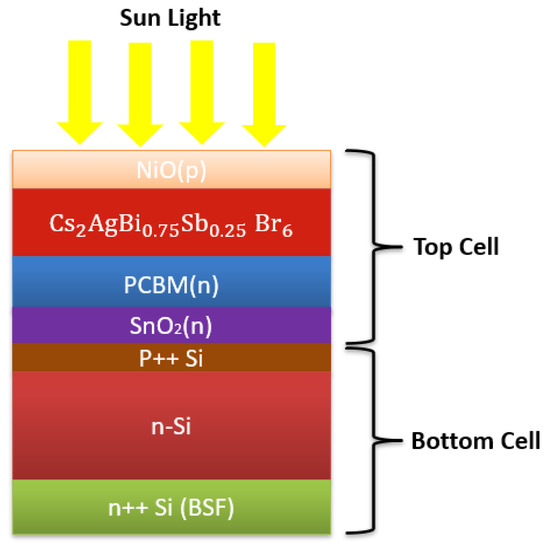
Figure 1.
Tandem solar cell structure based on a bottom sub-cell of n-type silicon and a top cell of lead-free perovskite (hole transport layer: NiO; absorber: Cs2AgBi0.75Sb0.25Br6; electron transport layers: PCBM and SnO2).
As explained below, this structure has been well studied by various authors, as it appears promising for the production of a highly efficient solar cell with improved stability. In the following, we review some interesting properties of this structure that explain the interest that it has received in the literature. We start with the SnO2 layer and its function as the ETM layer. When SnO2 is used as the ETM layer, it reduces the hysteresis effect due to its higher conductivity and good electron mobility. These electronic characteristics facilitate the transfer of charges from the perovskite absorber layer to the ETM layer, resulting in a decrease in the charge accumulation at the interface of these two layers and therefore limiting the hysteresis effect. In addition, the advantageous properties of SnO2 that enhance the stability of the hole device are retained in oxygen and moisture conditions [28]. Additionally, Fang et al. [29] determined that when using a hierarchical SnO2 nanosheet as the ETM, the device preserved 90% of its initial efficiency, even after 3000 h of storage without encapsulation. Then, by adding the PCBM layer, the perovskite solar cell performance can be further enhanced. In fact, the SnO2/PCBM bilayer has been the best cooperative combination that has been extensively developed, as shown by Wang et al. [30]. It is reported that fullerene can redissolve during the deposition of perovskite, allowing a fraction of ultra-thin fullerene elements to remain at the interface and another fraction to penetrate perovskite grain boundaries. As a result, the SnO2 layer efficiently traps holes, while the fullerenes allow the electron transfer while passivating the interface of SnO2/perovskite and the perovskite grain boundaries [31]. Finally, in the proposed structure, a surface layer of NiO caps the PSC. When NiO was used as the hole transport material (HTM), simulations and experiments showed that the stability of the solar cell was substantially increased owing to its p-type characteristics, such as a wide bandgap (Eg) exceeding 3.50 eV, good conductivity, significant optical transmittance, and suitable energy-level alignment with different absorbers [29]. It has been reported that PSCs with NiO as the HTM layer have a high stability, i.e., over 90% for almost 60 days of storage in air [32]. The bottom sub-cell based on n-type silicon is considered the most efficient candidate due to its well-known advantageous properties provided by the n-type crystalline silicon substrate itself. In addition to all of the effective properties described above, we can also cite the absence of defects related to boron-oxygen. n-type crystalline silicon substrates are also highly tolerant to metal impurities [33].
The electrical parameters of all materials used in this simulation are summarized in Table 1 and reported in [16,34,35,36,37,38,39].

Table 1.
Basic electrical properties of the materials used in the proposed structure [16,34,35,36,37,38,39].
The simulation was performed with the SCAPS-1D simulator to study and optimize the optical and electrical parameters of the solar cells investigated in the current work for the considered tandem cell. The SCAPS software was developed by the University of Ghent, Belgium [40]. It enables the calculation of the functional parameters of photovoltaic cells, i.e., the short-circuit current, the open-circuit voltage, the fill factor, and the PCE as a function of the intrinsic parameters of the cells, i.e., the band structure, the electric field distribution, the capacitance, the generation and recombination profiles, and the light bias, and as function of external physical parameters such as the temperature and illumination spectrum. The simulation results obtained in this work using the SCAPS-1D simulator on the perovskite/silicon tandem solar cell were validated by comparing them with experimental values reported in the literature [16,26].
On the basis of these fundamental material parameters, the studied tandem cell was calibrated. We started the calibration under the standalone condition for both the top and bottom sub-cells, and then the whole tandem cell was simulated under the standard AM 1.5 G spectrum. In 2T tandem devices, the tunnel recombination junction results in the same short-circuit current, JSC, in both top and bottom sub-cells. Owing to the limitations of the SCAPS-1D simulator, an ideal tunnel junction is assumed between the top and bottom sub-cells without opto-electrical losses due to reflections at the interfaces between layers. The transmitted spectrum from the top to the bottom sub-cell is described by Equation (1) [41]:
where S0(λ) represents the incident AM 1.5 spectrum, λ is the wavelength, α is the absorption coefficient, and d is the thickness of the different materials forming the perovskite top sub-cell. materiali refers to NiO, perovskite, PCBM, or SnO2.
To study the performance of the whole tandem cell, after the independent simulation of individual sub-cells, we considered the top cell to be illuminated under the standard AM 1.5 spectrum, as shown in Figure 2a. The filtered spectrum that reaches the bottom sub-cell is shown in Figure 2b, which was obtained using Equation (1) with different absorption coefficients and thicknesses of the top sub-cell layers as presented in Figure 3.
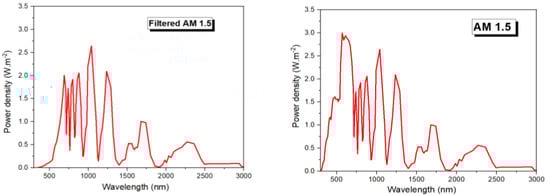
Figure 2.
(a) AM 1.5 spectrum absorbed by the perovskite top sub-cell and (b) filtered AM 1.5 absorbed by the silicon bottom sub-cell obtained with Equation (1).
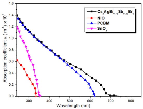
Figure 3.
Absorption coefficients of Cs2AgBi0.75 Sb0.25 Br6, NiO, PCBM and SnO2 used in simulation and for the calculation of filtered spectrum.
The notable changes in the incident spectrum (Figure 2a) due to absorption by the top sub-cell, as observed in the spectrum in Figure 2b, mainly involve the UV and near-UV ranges of the spectrum, which explains why the combination of this type of PSC with a silicon cell is not active in this wavelength range.
With the current matching technique, the filtered spectrum in Figure 2b was used to simulate the bottom sub-cell and then the whole tandem cell [26,42].
The top and bottom sub-cells were calibrated on the basis of information related to the cells manufactured and reported in [16] (for the top sub-cell) and [26] (for the bottom sub-cell) with the parameters introduced in Table 1. In this regard, the current density–voltage (J–V) curve and external quantum efficiency (EQE) of the standalone top and bottom sub-cells were obtained and are reported in Figure 4a,b, respectively.
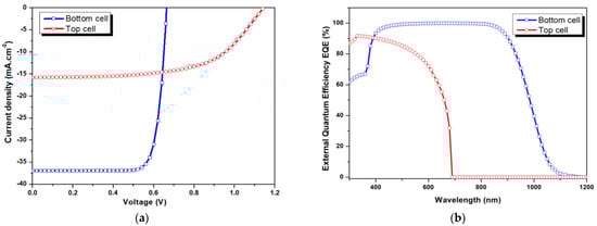
Figure 4.
(a) J–V curve of silicon bottom sub-cell and perovskite top sub-cell (b); external quantum efficiency (EQE) of the two sub-cells in standalone conditions.
As shown in Figure 4a, with the parameters of Table 1 and thus with different initial thicknesses of the layers, the top and bottom sub-cells have a JSC of 15.37 mA.cm–2 and 37.8 mA.cm–2 and a VOC of 1.14 V and 0.66 V, respectively. Further, the top sub-cell achieves more than 80% EQE at a wavelength of 400 nm, which then falls below 60% for wavelengths above 650 nm. This is attributed to the high bandgap (1.8 eV) of the perovskite layer. The simulated value of EQE measured at 1.8 eV for the top sub-cell is in good agreement with the EQE determined experimentally by Eperon et al. [13]. The cut-off wavelength for EQE is 50% higher in the bottom sub-cell, which results in a higher JSC, as shown in Figure 4a. The photovoltaic parameters of both sub-cells obtained in standalone conditions in the present work and the results obtained experimentally and reported in the literature are summarized in Table 2.
Table 2.
Numerical (current work) and experimental photovoltaic parameters for the top and the bottom sub-cells considered in standalone conditions with the parameters and thicknesses reported in the literature and listed in Table 1.
We observe that all of the photovoltaic parameters obtained in the simulations are very close to those obtained experimentally, but the simulated values are always superior. For example, the Jsc simulated in the present work is slightly greater than the experimentally measured value. This discrepancy in the current density is attributed to the lower power density received by the absorber layer in real cells due to the presence of metal contacts [40]. Therefore, these differences in voltages and currents explain the differences observed in the FF and in the PCE between the two approaches. Taking into account possible experimental errors in the measurements reported in the literature, we conclude that the calibration of the top and bottom sub-cells in our work closely reflects the real values.
3. Optimization of Sub-Cell Parameters in Standalone Conditions
3.1. Effects of the Silicon Absorber Layer Thickness and the BSF Dopant Concentration on the Bottom Sub-Cell
To improve the current balance between the two sub-cells, we varied the thickness of the bottom cell as the first adjustable parameter.
In this study, the thickness of the silicon absorber layer varied from 10 to 80 μm. The J–V curve and EQE(λ) of the bottom cell for different thicknesses are reported in Figure 5a,b respectively. Figure 6 shows the dependence of the functional parameters Jsc, Voc, FF, and PCE on the thickness of this silicon absorber layer.
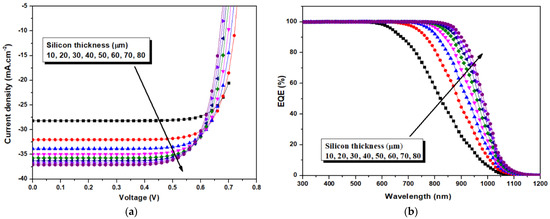
Figure 5.
Effect of the n-type silicon layer thickness in standalone conditions on (a) the J–V curve (b) the external quantum efficiency (EQE).
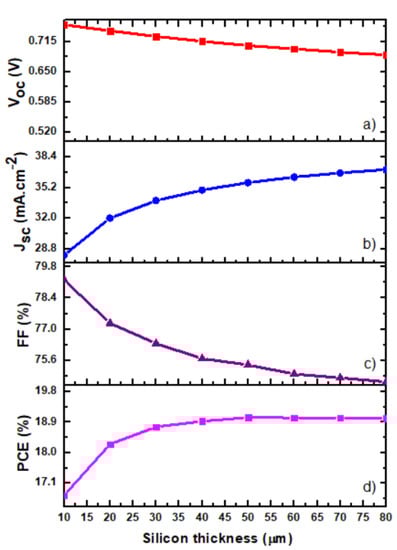
Figure 6.
Effect of absorber layer thickness on the solar cell parameters.
The external quantum efficiency of a photovoltaic cell is defined as the ratio of the short-circuit current JSC(λ) to the incident photon flux Φ(λ) at a given energy multiplied by the electronic charge q [43]:
According to Figure 6, we observe that Jsc increases to a greater extent than Voc, which only increases slightly with the thickness of the absorber layer. As a result, that the thickness of the absorber layer of the bottom cell determines the number of photons absorbed, especially for small dimensions up to a saturation value of the thickness, the EQE of the cell is also directly dependent. In addition, an absorber layer with a large thickness can maximize the capture of photons. As a direct consequence, as the thickness increases, the PCE increases, while the fill factor decreases. Therefore, the incident photon flux Φ0(λ) increases with the increase in the thickness of the absorber layer. It is also apparent that all functional parameters tend to saturation values, so instead of continuously increasing the thickness, it is necessary to find an optimum compromise in the physical and electrical parameters of the resulting tandem cell, as we describe below.
The back surface field (BSF) can enhance the efficiency of the solar cell. The minority carrier surface recombination at the rear surface is one of the different factors that leads to a decrease in the solar cell efficiency [44]. To minimize the surface recombination losses at the rear surface, another thin layer made of heavily doped n-type silicon was introduced to the back surface. In this way, the heavily doped layer creates a junction with the lightly doped absorption layer, i.e., n/n++, which is known as the back surface field (BSF). This junction pushes the minority carriers back to the absorbing layer and reduces the back surface recombination velocity (BSRV) to a greater degree, thus improving Jsc, Voc, FF, and ƞ. BSRV can be calculated following Equation (3).
where and are the dopant concentrations, is bandgap narrowing due to a high dopant concentration, T is the temperature, K represents Boltzmann’s constant, q is the electron charge, is the electron minority carrier diffusion length, is the BSF thickness, and is surface recombination velocity. The effect of the dopant concentration of BSF on the energy band diagram is shown in Figure 7, which compares two values of the BSF layer, ND = 1015 cm–3 and ND = 1022 cm–3.
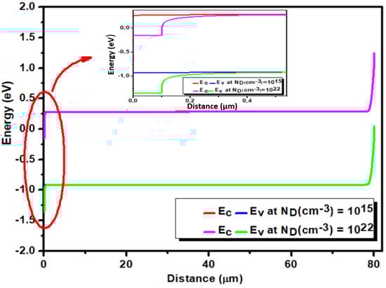
Figure 7.
Effect of the doping concentration on the energy band diagram of the bottom sub-cell.
We can observe that adding the BSF layer creates a field that reduces the transfer of the minority carriers to the back surface, and by increasing the dopant concentration of the BSF, we increase the field and enhance the solar cell performance. Figure 8 shows the effect of varying the dopant concentration of the BSF layer from ND = 1015 cm–3 to ND = 1022 cm–3, which are generally the values used in the experimental fabrication of the cell [45], on the J–V curve of the bottom solar sub-cell.
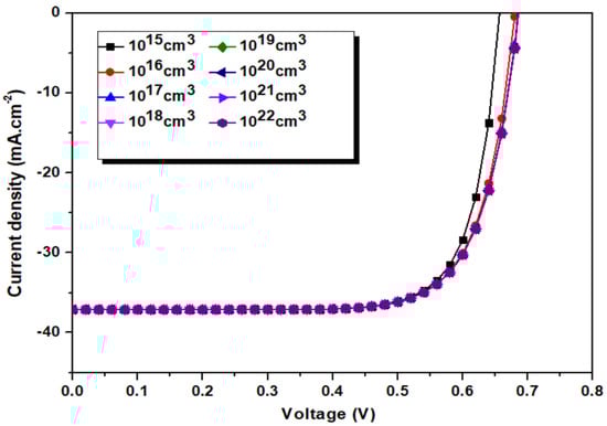
Figure 8.
Effect of the doping concentration on the J–V curve of the bottom sub-cell.
As the doping concentration increases, Jsc remains constant, while Voc increases due to the direct relationship shown in Equation (4).
where is the thermal voltage, Δn is the excess carrier concentration, ND is the doping concentration, and ni is the intrinsic carrier concentration.
Since Jsc remains constant and Voc increases, the PCE increases as well. According to these results, we fixed the dopant concentration of the BSF layer to 1022 cm–3. In Section 4, we analyze the effect of the dopant concentration of the BSF layer on the whole tandem device.
3.2. Effects of the Perovskite Absorber Layer Thickness of the Top Cell
The same simulation performed in standalone conditions for the bottom cell was reproduced for the top cell as a function of its perovskite absorber layer thickness. The J–V curve and EQE(λ) of the top cell are reported in Figure 9a,b, respectively, and the dependence of the functional parameters Jsc, Voc, FF, and PCE on the thickness of this perovskite absorber layer is illustrated in Figure 10.
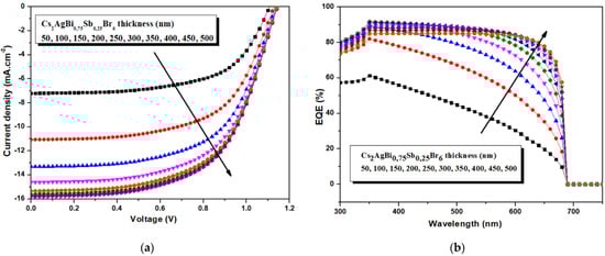
Figure 9.
Effect of the standalone perovskite absorber layer thickness on (a) the J–V curve and (b) external quantum efficiency.
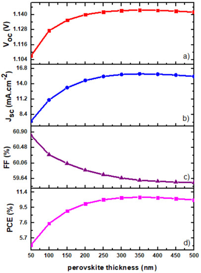
Figure 10.
Effect of thickness of the perovskite absorber layer on the solar cell. parameters.
It is noted that increasing the active layer thickness leads to an increase in the current density due to the high absorption in the active region. Therefore, a large number of electron–hole pairs are generated. The subsequent separation of the generated electron–hole pairs increase the JSC of the device. The improvement in Jsc and EQE is significant at lower thicknesses and begins to saturate as thickness increases. This improvement of EQE is mainly noticeable for longer wavelengths since low wavelength photons are absorbed near the surface, whereas a thicker absorbent layer is necessary to absorb photons with higher wavelengths. Figure 10 shows that Voc does not significantly increase as the thickness of the absorbent layer increases: Voc increases by 2% when the thickness increases from 100 nm to 500 nm. Due to the increase in the resistance with the absorber thickness, the fill factor decreases from 60.2% to 59% when the thickness changes from 100 nm to 500 nm. Although there is a small reduction in FF, all of the other parameters increase, and thus, the overall performance of the cell improves. In the same range for the absorber thickness, the PCE increases from 7% to 10%. Our results are confirmed by other reported data, such as the recent work of Madan et al. [21].
4. Lead-Free Perovskite/Silicon Tandem Solar Cell
4.1. Combined Effect of the Thicknesses of the Two Absorber Layers on the Performance of the Tandem Cell
After the above analysis and evaluation of the functional properties of both sub-cells in standalone conditions, simulations were performed to study the complete tandem solar cell. The approach to simulating the tandem device is discussed in the previous section on device structure and parameters. In this simulation, the AM 1.5 spectrum was illuminated towards the top sub-cell, and the transmitted spectrum S(λ) was calculated using the absorption coefficients and the thicknesses of all layers of the top sub-cell, as shown in Equation (1) and in the resulting spectrum in Figure 2b.
In the next simulation, the absorber layer thickness of the top sub-cell was varied from 100 nm to 500 nm, while the thicknesses of the rest of the layers remained constant. The transmitted spectrum filtered by the top sub-cell at different absorber layer thicknesses is shown in Figure 11. The result shows that, in the whole spectral range, the transmitted optical power density (W.m−2) is significantly attenuated with the increasing thickness of the absorber layer of the top sub-cell.
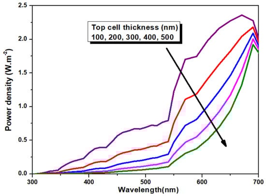
Figure 11.
Transmitted spectrum by the top sub-cell for different thicknesses of the absorber of the top sub-cell.
These filtered spectra were used to illuminate the bottom sub-cell and to study the optical coupling of photons in the two sub-cells. The photocurrent absorbed in the top sub-cell is lower with a thin absorber base (50 nm thick), resulting in a higher transmitted photocurrent to the bottom sub-cell. Increasing the top sub-cell thickness to greater than 400 nm reduces the transmitted photocurrent.
Considering the influence of the thicknesses of the absorber of both sub-cells, thus taking into account the filtered spectrum that reaches the bottom cell, JSC, Voc, and PCE of the tandem cell are discussed based on the 3D contour plots of these parameters in Figure 12a and Figure 13a,b.
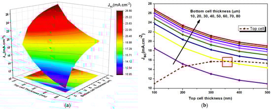
Figure 12.
(a) The 3D contour plot of Jsc of the tandem cell at different thicknesses of the absorber layers of both sub-cells. (b) Jsc for top and bottom sub-cells as a function of both absorber thicknesses. The optimum pairing is highlighted by the red square.
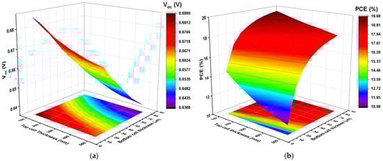
Figure 13.
The 3D contour plot of PV parameters for the bottom cell: (a) Voc and (b) PCE at different thicknesses of the absorber layer in the top and bottom cells.
First, we discuss the influence of the thickness of the absorbers of the two sub-cells on the short-circuit current of the tandem cell. As observed in the results reported in Figure 12a, for an absorber of the top sub-cell with low thickness, a high JSC value is transmitted to the bottom sub-cell. This current begins to decrease as the thickness of this layer in the top sub-cell increases. Conversely, for a given thickness of the absorber of the top sub-cell, increasing the thickness of the absorber of the bottom sub-cell increases JSC. Therefore, a compromise in the thicknesses of the two absorbers must be found to optimize the performance of the final tandem cell. This optimization has to account for the fact that the 2T tandem solar cell acts as two diodes connected in series. As mentioned in the introduction, this 2T structure makes it possible to ensure that the same current flows through the two sub-cells; in other words, the total value of Voc is the sum of the individual Voc of each sub-cell, but the sub-cell with the lowest value of JSC limits the overall JSC of the tandem device [46]. Therefore, in tandem devices, the thicknesses of the different layers must be optimized to have the same JSC value passing through the two sub-cells and to facilitate the tunnel recombination junctions used [47,48].
As the thickness of the layers in the top sub-cell decrease below a threshold value, the absorption is reduced, resulting in a reduction in the overall JSC of the tandem cell. Similarly, if the thickness of the layer in the top sub-cell increases beyond a threshold value, the absorption will decrease the optical coupling in the bottom sub-cell, which also results in a decrease in the overall JSC of the tandem cell. These observations allow us to establish the current matching conditions to obtain the same JSC value in the two sub-cells.
Next, we used the spectra filtered by the absorber layer of the top sub-cell for different thicknesses (Figure 11) as input data to evaluate the PV parameters of the bottom sub-cell. The thickness of the bottom sub-cell was varied from 10 to 80 µm. The bottom sub-cell JSC values, obtained from the spectrum filtered by the top sub-cell, were used to determine the optimum pairing condition for the tandem device, as shown in Figure 12b. The best current matching condition that provides a higher equivalent value for both sub-cells is highlighted by the red square in Figure 12b and is obtained with a top sub-cell thickness of 380 nm and a bottom cell thickness of 20 µm, yielding JSC values equal to 16.01 mA.cm–2 and 16.09 mA.cm–2, respectively.
Further, apart from the current pairing condition discussed above, Figure 13a shows that the top sub-cell has a marginal influence on the total Voc of the tandem cell, unlike the bottom sub-cell, in which Voc strongly decreases with the increase in its thickness. The PCE of the tandem cell is shown in Figure 13b. The influence of the thickness of the absorbers of the two sub-cells is clearly demonstrated by the doubling of the PCE for the evaluated thicknesses. A PCE value of 15.56% is obtained with the current matching condition, i.e., for thicknesses that produce an optimum JSC throughout the tandem cell structure. With the absorber thicknesses optimized for the current pairing condition, as discussed above, a perovskite/silicon tandem solar cell was simulated.
The effect of the BSF layer dopant concentration, as discussed above, was also measured for the global tandem solar cell. The J–V curves of the tandem solar cell are presented in Figure 14 for two extremum values of possible dopant concentrations in the BSF layer.
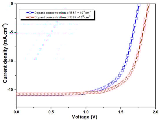
Figure 14.
The I–V characteristic of the optimized tandem solar cell.
As observed from the results, for the optimal dopant concentration of the BSF layer, ND = 1022 cm–3, the open-circuit voltage of the tandem device increases.
The J–V characteristics of the top sub-cell, the bottom sub cell, and the tandem cell are presented in Figure 15, and the photovoltaic parameters are reported in Table 3.
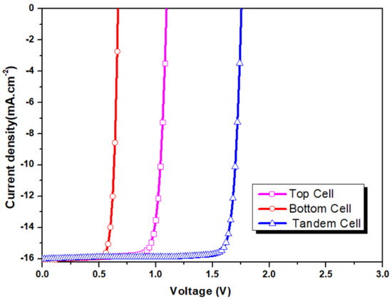
Figure 15.
The J–V characteristic of the optimized tandem solar cell.
Table 3.
Photovoltaic parameters of the top, bottom, and tandem cells.
After the full optimization of the two sub-cells in current matching conditions, particularly the absorber layer thicknesses and the dopant concentration of the BSF layer, the tandem solar cell achieves a short current circuit equal to 16.01 mA.cm–2 and an open-circuit voltage of 1.76 V, yielding a PCE of 24.4% at room temperature (T = 300 K) and for AM 1.5G.
This performance makes this solar cell structure an interesting alternative that provides high efficiency, better stability, and a lower cost of fabrication compared to traditional silicon solar cells and III–V semiconductors.
To further understand our study of this tandem solar cell configuration, the effect of the working temperature on the solar cell efficiency is simulated in the next section.
4.2. Effect of the Working Temperature on the Parameters of the Optimized Tandem Solar Cell
In most cases, solar cells are used in outdoor environments and are exposed to sunlight, which can increase the temperature by as much as 273.15 K above ambient temperature [49]. For this reason, various experiments have shown that the most difficult challenge for PSCs is long-term stability [50,51]. Since the analysis of temperature effects is very important, we simulated the effect of working temperature on the lead-free perovskite top sub-cell in the standalone condition and its effect on the tandem solar cell. It is reported in the literature that Cs2AgBiBr6 shows a better mechanical and thermal performance as compared to other MAPbBr3-type perovskites. The strong Ag–Br and Bi–Br bonds increase the rigidity of Cs2AgBiBr6, while the Pb–X bonds (X = Cl, Br, or I) in metal halide perovskites are relatively weak. This perovskite is mainly characterized by its low thermal expansion behavior, which reduces thermal stresses that arise during the processing or operation of the cell, improving the device life [52,53]. The effect of the working temperature on the perovskite top sub-cell was simulated, and the associated J–V curve is presented in Figure 16.
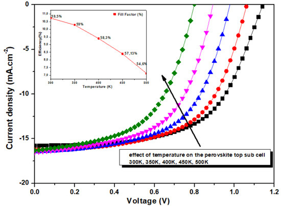
Figure 16.
Effect of the working temperature on the J–V curve of the perovskite top sub-cell.
We observe that increasing the temperature results in a decrease in the solar cell efficiency. Comparing this decrease with that obtained when simulating lead halide perovskite solar cells, it is observed that lead-free perovskite cells are less affected by the increase in temperature. In fact, by increasing the temperature from 300 K to 350 K, a decrease of 0.45% in solar cell efficiency is observed, which is much less than the 5% drop in efficiency obtained by Abdulsalam et al. [54] when simulating the effect of the temperature on MAPBI3 perovskite solar cells.
Figure 17 shows the J–V curve of the tandem solar cell when varying the temperature from 300 K to 500 K.
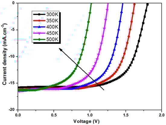
Figure 17.
Effect of the working temperature on the J–V curve of the tandem solar cell.
The performance of the solar cell is affected by the increasing temperature, which is linked to open-circuit voltage decay. Voc is reduced because of its direct link to reverse saturation current density (Jo), which is further related to intrinsic carrier concentration ‘ni’. ni depends on the energy bandgap, i.e., = , where k1 is a constant and Eg is inversely proportional to the temperature, as given by Equation (5):
where Eg(T) is the bandgap of the material at temperature T, and α and β are constants.
The results show that PCE and FF also decrease. The high temperature leads to more excited electrons, but the bandgap can be unstable, resulting in the strong recombination of carriers and thus reducing the efficiency.
5. Conclusions
Simulations were performed to optimize the photovoltaic parameters of a tandem lead-free perovskite/silicon solar cell with the aim of improving the efficiency and stability of commercial devices. The top lead-free perovskite Cs2AgBi0.75Sb0.25Br6 sub-cell and the bottom n-type silicon sub-cell were first simulated under standalone conditions. Then, we aimed to optimize the thicknesses of the two absorbers to obtain current matching by simulating the J–V curve of the lower silicon sub-cell using the spectrum filtered by the top sub-cell. The optimal thicknesses of top/bottom sub-cells are 380 nm/20 µm, respectively, and the optimal dopant concentration of the BSF layer of the silicon sub-cell is equal to 1022 cm–3. The optimized tandem solar cell achieves a large open-circuit voltage of 1.76 V, a short-circuit current of 16.01 mA.cm–2, and a PCE of 24.4%. In addition, the effect of the working temperature was simulated, and the results show the advantages of the lead-free perovskite tandem solar cell, which combines satisfactory thermal expansion behavior and electrical parameter values and efficiency that are very competitive with standard silicon cells. The nontoxicity and impressive moisture stability of this type of lead-free perovskite/silicon tandem solar cell make it a strong candidate for potential applications in optoelectronics and photovoltaics.
Author Contributions
Conceptualization, K.A. and M.A.; data curation, K.A., R.B. and M.A.; formal analysis, K.A., R.B. and M.A.; funding acquisition, R.G. and M.A.; investigation, K.A., R.B. and M.A.; methodology, K.A. and R.B.; resources, K.A. and M.A.; writing—original draft preparation, K.A.; writing—review, R.B. and M.A.; editing, M.A. All authors have read and agreed to the published version of the manuscript.
Funding
This research received no external funding.
Acknowledgments
The team of authors acknowledges Marc Burgelman and his staff at the University of Gent, Belgium, for providing the open-source SCAPS-1D simulator.
Conflicts of Interest
The authors declare no conflict of interest.
References
- Reyes-Belmonte, M.A. Quo Vadis Solar Energy Research. Appl Sci. Multidiscip. Digit. Publ. Inst. 2021, 11, 3015. [Google Scholar]
- Miller, O.D.; Yablonovitch, E. Photon extraction: The key physics for approaching solar cell efficiency limits. Act Photonic Mater V [Internet]. International Society for Optics and Photonics. Available online: https://www.spiedigitallibrary.org/conference-proceedings-of-spie/8808/880807/Photon-extraction--the-key-physics-for-approaching-solar-cell/10.1117/12.2024592.short (accessed on 1 June 2021).
- Todorov, T.; Gunawan, O.; Guha, S. A road towards 25% efficiency and beyond: Perovskite tandem solar cells. Mol. Syst Des. Eng. R. Soc. Chem. 2016, 1, 370–376. [Google Scholar] [CrossRef]
- Rideout, V.L. A review of the theory and technology for ohmic contacts to group III–V compound semiconductors. Solid-State Electron. 1975, 18, 541–550. [Google Scholar] [CrossRef]
- Eperon, G.E.; Hörantner, M.T.; Snaith, H.J. Metal halide perovskite tandem and multiple-junction photovoltaics. Nat. Rev. Chem. Nat. Publ. Group 2017, 1, 1–18. [Google Scholar] [CrossRef]
- Leijtens, T.; Bush, K.A.; Prasanna, R.; McGehee, M.D. Opportunities and challenges for tandem solar cells using metal halide perovskite semiconductors. Nat. Energy Nat. Publ. Group 2018, 3, 828–838. [Google Scholar] [CrossRef]
- Wali, Q.; Elumalai, N.K.; Iqbal, Y.; Uddin, A.; Jose, R. Tandem perovskite solar cells. Renew. Sustain. Energy Rev. 2018, 84, 89–110. [Google Scholar] [CrossRef]
- Stranks, S.D.; Eperon, G.E.; Grancini, G. Electron-Hole Diffusion Lengths Exceeding 1 Micrometer in an Organometal Trihalide Perovskite Absorber. Science 2013. [Google Scholar] [CrossRef]
- Ponseca, C.S.; Savenijie, T.J.; Abdellah, M. Organometal Halide Perovskite Solar Cell Materials Rationalized: Ultrafast Charge Generation, High and Microsecond-Long Balanced Mobilities, and Slow Recombination. J. Am. Chem. Soc. 2014. [Google Scholar] [CrossRef]
- Zhu, S.; Yao, X.; Ren, Q.; Zheng, C.; Li, S.; Tong, Y.; Shi, B.; Guo, S.; Fan, L.; Ren, H.; et al. Transparent electrode for monolithic perovskite/silicon-heterojunction two-terminal tandem solar cells. Nano Energy 2018, 45, 280–286. [Google Scholar] [CrossRef]
- Eperon, G.E.; Stranks, S.D.; Menelaou, C.; Johnston, M.B.; Herz, L.M.; Snaith, H.J. Formamidinium lead trihalide: A broadly tunable perovskite for efficient planar heterojunction solar cells. Energy Environ. Sci. R. Soc. Chem. 2014, 7, 982–988. [Google Scholar] [CrossRef]
- Zhou, H.; Li, C.; Luo, S. Interface engineering of highly efficient perovskite solar cells. Science 2014. [Google Scholar] [CrossRef] [PubMed]
- Best Research-Cell Efficiency Chart. Available online: https://www.nrel.gov/pv/cell-efficiency.html (accessed on 28 March 2021).
- Li, Z.; Klein, T.R.; Kim, D.H.; Yang, M.; Berry, J.J.; Van Hest, M.F.A.M.; Zhu, K. Scalable fabrication of perovskite solar cells. Nat. Rev. Mater. Nat. Publ. Group 2018, 3, 1–20. [Google Scholar] [CrossRef]
- Reese, M.O.; Glynn, S.; Kempe, M.D.; McGott, D.L.; Dabney, M.S.; Barnes, T.M.; Booth, S.; Feldman, D.; Haegel, N.M. Increasing markets and decreasing package weight for high-specific-power photovoltaics. Nat. Energy. Nat. Publ. Group 2018, 3, 1002–1012. [Google Scholar] [CrossRef]
- Eperon, G.E.; Leijtens, T.; Bush, K.A. Perovskite-perovskite tandem photovoltaics with optimized band gaps. Science 2016. [Google Scholar] [CrossRef] [PubMed]
- Forgács, D.; Gil-Escrig, L.; Pérez-Del-Rey, D.; Momblona, C.; Werner, J.; Niesen, B.; Ballif, C.; Sessolo, M.; Bolink, H.J. Efficient Monolithic Perovskite/Perovskite Tandem Solar Cells. Adv. Energy Mater. 2017, 7, 1602121. [Google Scholar] [CrossRef]
- Rajagopal, A.; Yang, Z.; Jo, S.B. Highly Efficient Perovskite–Perovskite Tandem Solar Cells Reaching 80% of the Theoretical Limit in Photovoltage—Rajagopal—2017. Adv. Mater. Wiley Online Libr. 2017. [Google Scholar] [CrossRef]
- Ali, R.; Hou, G.-J.; Zhu, Z.-G.; Yan, Q.-B.; Zheng, Q.-R.; Su, G. Stable mixed group II (Ca, Sr) and XIV (Ge, Sn) lead-free perovskite solar cells. J. Mater. Chem A. R. Soc. Chem. 2018, 6, 9220–9227. [Google Scholar] [CrossRef]
- McClure, E.T.; Ball, M.R.; Windl, W. Woodward PM. Cs2AgBiX6 (X = Br, Cl): New Visible Light Absorbing, Lead-Free Halide Perovskite Semiconductors. Chem. Mater. Am. Chem. Soc. 2016, 28, 1348–1354. [Google Scholar]
- Madan, J.; Shivani Pandey, R.; Sharma, R. Device simulation of 17.3% efficient lead-free all-perovskite tandem solar cell. Sol. Energy 2020, 197, 212–221. [Google Scholar] [CrossRef]
- Almansouri, I.; Ho-Baillie, A.W.Y.; Green, M.A. Ultimate Efficiency Limit of Single-Junction Perovskite and Dual-Junction Perovskite/Silicon Two-Terminal Devices—IOPscience. Available online: https://iopscience.iop.org/article/10.7567/JJAP.54.08KD04/meta (accessed on 28 March 2021).
- Mailoa, J.; Bailie, C.; Johlin, E.; Hoke, E.; Akey, A.; Nguyen, W.; Mc Gehee, M.D.; Buanassisi, T. A 2-Terminal Perovskite/Silicon Multijunction Solar Cell Enabled by a Silicon Tunnel Junction. Appl. Phys. Lett. 2015, 106, 121105. [Google Scholar] [CrossRef]
- Werner, J.; Weng, C.-H.; Walter, A. Efficient Monolithic Perovskite/Silicon Tandem Solar Cell with Cell Area >1 cm2. J. Phys. Chem. Lett. 2016. [Google Scholar] [CrossRef] [PubMed]
- Zhong, Y.; Hufnagel, M.; Thelakkat, M.; Li, C.; Huettner, S. Role of PCBM in the Suppression of Hysteresis in Perovskite Solar Cells. Adv Funct Mater. 2020, 30, 1908920. [Google Scholar] [CrossRef]
- Schmiga, C.; Nagel, H.; Schmidt, J. 19% efficient n-type Czochralski silicon solar cells with screen-printed aluminium-alloyed rear emitter—Schmiga—2006—Progress in Photovoltaics. Res. Appl. Wiley Online Libr. 2006. [Google Scholar] [CrossRef]
- Zheng, J.; Lau, C.F.J.; Mehrvarz, H.; Ma, F.-J.; Jiang, Y.; Deng, X.; Soeriyadi, A.; Kim, J.; Zhang, M.; Hu, L.; et al. Large area efficient interface layer free monolithic perovskite/homo-junction-silicon tandem solar cell with over 20% efficiency. Energy Environ. Sci. R. Soc. Chem. 2018, 11, 2432–2443. [Google Scholar] [CrossRef]
- Tiwana, P.; Docampo, P.; Johnston, M.B.; Snaith, H.J.; Herz, L.M. Electron mobility and injection dynamics in mesoporous ZnO, SnO2, and TiO2 films used in dye-sensitized solar cells. ACS Nano 2011, 5, 5158–5166. [Google Scholar] [CrossRef]
- Wang, S.; Zhu, Y.; Liu, B.; Wang, C.; Ma, R. Introduction of carbon nanodots into SnO2 electron transport layer for efficient and UV stable planar perovskite solar cells. J. Mater. Chem. A. 2019, 7. [Google Scholar] [CrossRef]
- Wang, J.; Datta, K.; Weijtens, C.H.L.; Wienk, M.M.; Janssen, R.A.J. Insights into Fullerene Passivation of SnO2 Electron Transport Layers in Perovskite Solar Cells. Adv. Funct. Mater. 2019, 29, 1905883. [Google Scholar] [CrossRef]
- Ke, W.; Zhao, D.; Xiao, C.; Wang, C.; Cimaroli, A.J.; Grice, C.R.; Yang, M.; Li, Z.; Jiang, C.-S.; Al-Jassim, M.; et al. Cooperative tin oxide fullerene electron selective layers for high-performance planar perovskite solar cells. J. Mater. Chem. A. R. Soc. Chem. 2016, 4, 14276–14283. [Google Scholar] [CrossRef]
- You, J.; Meng, L.; Song, T.B.; Guo, T.F.; Yang, Y.M.; Chang, W.H.; Hong, Z.; Chen, H.; Zhou, H.; Chen, Q.; et al. Improved air stability of perovskite solar cells via solution-processed metal oxide transport layers. Nat. Nanotechnol. 2016, 11, 75–81. [Google Scholar] [CrossRef]
- Attequr, R.; Soo Hong, L. Advancements in n-Type Base Crystalline Silicon Solar Cells and Their Emergence in the Photovoltaic Industry. Sci. World J. 2013. [Google Scholar] [CrossRef]
- Dong, H.; Pang, S.; Zhang, Y.; Chen, D.; Zhu, W.; Xi, H.; Chang, J.; Zhang, J.; Zhang, C.; Hao, J. Improving Electron Extraction Ability and Device Stability of Perovskite Solar Cells Using a Compatible PCBM/AZO Electron Transporting Bilayer. Nanomater. Multidiscip. Digit. Publ. Inst. 2018, 8, 720. [Google Scholar] [CrossRef] [PubMed]
- Gao, H.; Qin, C.; Zhang, H.; Wu, S. Theoretical Characterization of a Typical Hole/Exciton-Blocking Material Bathocuproine and Its Analogues. J. Phys. Chem. A 2008. [Google Scholar] [CrossRef] [PubMed]
- Kim, K.; Lee, J.W.; Lee, S.H.; Lee, Y.B.; Cho, E.H.; Noh, H.-S.; Jo, S.G.; Joo, J. Nanoscale optical and photoresponsive electrical properties of P3HT and PCBM composite nanowires. Org. Electron. 2011, 12, 1695–1700. [Google Scholar] [CrossRef]
- Minbashi, M.; Ghobadi, A.; Ehsani, M.H.; Rezagholipour Dizaji, H.; Memarian, N. Simulation of high efficiency SnS-based solar cells with SCAPS. Sol. Energy. 2018, 176, 520–525. [Google Scholar] [CrossRef]
- Hutchby, J.A.; Markunas, R.J.; Bedair, S.M. Material Aspects Of The Fabrication Of Multijunction Solar Cells. Photovoltaics. In International Society for Optics and Photonics; 1985; p. 40. Available online: https://www.spiedigitallibrary.org/conference-proceedings-of-spie/0543/0000/Material-Aspects-Of-The-Fabrication-Of-Multijunction-Solar-Cells/10.1117/12.948195.short (accessed on 5 April 2021).
- NMendil, D.M.; Berkai, Z. Study of PEDOT: PSS and BCP Thicknesses Effect on SubPc/C60 Organic Solar Cell Efficiency. Available online: https://www.spiedigitallibrary.org/conference-proceedings-of-spie/9567/1/Study-of-PEDOT--PSS-and-BCP-thicknesses-effect-on/10.1117/12.2188651.short?SSO=1 (accessed on 28 March 2021).
- Burgelman, M.; Nollet, P.; Degrave, S. Modelling polycrystalline semiconductor solar cells. Thin Solid Films. 2000, 361–362, 527–532. [Google Scholar] [CrossRef]
- Kim, K.; Yoo, J.S.; Ahn, S.K.; Eo, Y.J.; Cho, J.S.; Gwak, J.; Yun, J.H. Performance prediction of chalcopyrite-based dual-junction tandem solar cells. Sol. Energy 2017, 155, 167–177, Pergamon Elsevier Science Ltd.: Oxford, UK. [Google Scholar] [CrossRef]
- Gupta, G.K.; Dixit, A. Theoretical studies of single and tandem Cu2ZnSn(S/Se)4 junction solar cells for enhanced efficiency. Opt. Mater. 2018, 82, 11–20. [Google Scholar] [CrossRef]
- Herguth, A. On the meaning(fullness) of the intensity unit ‘suns’ in light induced degradation experiments. Energy Procedia. 2017, 124, 53–59. [Google Scholar] [CrossRef]
- Chung, S.-Y.; Jin, N.; Rice, A.T.; Berger, P.R.; Yu, R.; Fang, Z.-Q.; Thompson, P.E. Growth temperature and dopant species effects on deep levels in Si grown by low temperature molecular beam epitaxy. J. Appl Phys. Am. Inst. Phys. 2003, 93, 9104–9110. [Google Scholar] [CrossRef]
- Chen, B.; Rudd, P.N.; Yang, S.; Yuan, Y.; Huang, J. Imperfections and their passivation in halide perovskite solar cells. Chem Soc. Rev. R. Soc. Chem. 2019, 48, 3842–3867. [Google Scholar] [CrossRef]
- Kim, K.; Gwak, J.; Ahn, S.K.; Eo, Y.-J.; Park, J.H.; Cho, J.-S.; Kang, M.G.; Song, H.E.; Yun, J.H. Simulations of chalcopyrite/c-Si tandem cells using SCAPS-1D. Sol. Energy. 2017, 145, 52–58. [Google Scholar] [CrossRef]
- Gu, X.; Yu, X.; Yang, D. Efficiency improvement of crystalline silicon solar cells with a back-surface field produced by boron and aluminum co-doping. Scr. Mater. 2012, 66, 394–397. [Google Scholar] [CrossRef]
- Burdick, J.; Glatfelter, T. Spectral response and I–V measurements of tandem amorphous-silicon alloy solar cells. Sol. Cells. 1986, 18, 301–314. [Google Scholar] [CrossRef]
- Leijtens, T.; Eperon, G.E.; Pathak, S.; Abate, A.; Lee, M.M.; Snaith, H.J. Overcoming ultraviolet light instability of sensitized TiO₂ with meso-superstructured organometal tri-halide perovskite solar cells. Nat. Commun. 2013, 4, 2885. [Google Scholar] [CrossRef]
- Han, Y.; Meyer, S.; Dkhissi, Y.; Weber, K.; Pringle, J.M.; Bach, U.; Spiccia, L.; Chneg, Y.-B. Degradation observations of encapsulated planar CH3NH3PbI3 perovskite solar cells at high temperatures and humidity. J. Mater. Chem. A. R. Soc. Chem. 2015, 3, 8139–8147. [Google Scholar] [CrossRef]
- Dong, L.; Sun, S.; Deng, Z.; Li, W.; Wei, F.; Qi, Y.; Li, J.; Li, X.; Lu, P.; Ramamurty, U. Elastic properties and thermal expansion of lead-free halide double perovskite Cs2AgBiBr. Comput. Mater. Sci. 2018, 141, 49–58. [Google Scholar] [CrossRef]
- Zheng, X.; Tang, L.; Zhang, D.; Dong, J.; Yang, H. Effect of contact spreading layer on photovoltaic response of InGaN-based solar cells. Phys. Status Solidi A. 2011, 208, 199–201. [Google Scholar] [CrossRef]
- Rothmann, M.U.; Li, W.; Zhu, Y.; Bach, U.; Spiccia, L.; Etheridge, J.; Cheng, Y.-B. Direct observation of intrinsic twin domains in tetragonal CH 3 NH 3 PbI. Nat. Commun. Nat. Publ. Group 2017, 8, 14547. [Google Scholar] [CrossRef] [PubMed]
- Abdulsalam, H.; Babaji, G.; Abba, H.T. The Effect of Temperature and Active layer thickness on the Performance of CH3NH3PbI3 Perovskite Solar Cell: A Numerical Simulation Approach. J. Found. Appl Phys. 2018, 5, 141–151. [Google Scholar]
Publisher’s Note: MDPI stays neutral with regard to jurisdictional claims in published maps and institutional affiliations. |
© 2021 by the authors. Licensee MDPI, Basel, Switzerland. This article is an open access article distributed under the terms and conditions of the Creative Commons Attribution (CC BY) license (https://creativecommons.org/licenses/by/4.0/).