Abstract
Extruded high voltage direct current (HVDC) cable systems contain interfaces with poorly understood microscopic properties, particularly surface roughness. Modelling the effect of roughness on conduction in cable insulation is challenging, as the available results of macroscopic measurements give little information about microscopic charge distributions at material interfaces. In this work, macroscopic charge injection from interfaces is assessed by using a bipolar charge transport model, which is validated against a series of space charge measurements on cable peelings with different degrees of surface roughness. The electric field-dependent conduction and charge trapping effects stimulated by the injection current originating from rough surfaces are assessed. It is shown that by accounting for roughness enhanced charge injection with the parameters derived in part I of the paper, reasonable agreement between computed and measured results can be achieved at medium field strengths (10–40 kV/mm).
1. Introduction
High voltage direct current (HVDC) cable systems allow for long-distance energy transmission and can be used as interconnectors between power grids or for offshore wind integration. While HVDC cables using conventional mass-impregnated or lapped paper insulation have been used reliably for a long time, recently developed insulation materials such as crosslinked polyethylene (XLPE) have been developed for a voltage level of 525 kV [1]. Such extruded HVDC cables are in high demand, owing to their cost-efficient jointing and manufacturing processes. To utilize their capacity to the fullest extent and to secure reliable operation, physical processes in extruded cable insulation stimulated by the combined effect of strong electric fields and thermal stresses need to be further understood.
An inherent feature of XLPE-based HVDC insulation systems is charge accumulation in the material due to long-lasting unipolar electric fields inducing the transport of charge carriers through the insulation. Elevated temperatures may intensify charge transfer locally, providing conditions for a strong space charge accumulation in the material. A correct description of the complex conduction physics is therefore necessary for anticipating internal charge dynamics and associated local electric fields, and to better understand the insulation’s capability to withstand elevated stress levels. While XLPE is an excellent insulator, owing to its specific semi-crystalline polymer structure and wide band gap that, however, leads to its complex electrical behavior. The amorphous and crystalline material phases exhibit differences in chain conformation, free volume, non-ideal bond density and impurity concentration, which can be expressed as states within the band gap, thereby defining inter-chain conduction of electrons and holes in the material.
The evolution of internal charges in the insulation is usually obtained from space charge measurements, such as the Pulsed Electro Acoustic (PEA) method. The PEA method acquires such measurement data by subjecting the material to voltage steps or pulses, causing a detectable acoustic signal originating from internal space charges in the material, as described in detail in part I of the paper. However, as discussed in part I, a multitude of effects may contribute to the results of such measurements, making direct clarification and quantification of the contributing effects challenging. Therefore, modelling of charge transport through the material under conditions that represent the experimental ones should be employed. In this way, the influence of different factors can be examined and quantified. Specifically, the impact of rough interfacial geometry on charge injection and local electric fields considered in part I of the paper can be implemented, focusing on accurate description of the injection–transport balance at the interfaces. Furthermore, as far as the behavior of the injected space charges and corresponding fields in the materials is understood, one may evaluate parameters of interest for cable operation, e.g., to predict lifetime and failure modes in XLPE insulation based on the previously observed dependency between surface roughness and breakdown voltages [2].
Following this approach, the purpose of this second part of the paper is to examine and to explain the results of the space charge measurements in XLPE by means of computer simulations of charge transport in the material focusing on surface roughness. For the simulations, the frequently used bipolar modelling approach [3,4,5,6,7,8,9,10,11] is adopted, which considers the field-induced dynamics of mobile and deeply trapped charge carriers within the material. To verify the model, the results of the simulations are compared with those obtained from the space charge measurements, which were carried out using the PEA method at polarizing fields in the range of 15–80 kV/mm and temperatures in the range of 25–70 °C. The experimental procedure including both the polarization stage and, additionally, the charge decay during depolarization was simulated utilizing wide-range field dependencies for all included effects, which were carefully evaluated. Furthermore, by comparing simulation results against the space charge measurements reported in part I, a set of parameters providing the best fit between the experimental and computed results was established.
2. Physical Background and Formulation of the Model
2.1. Fundamentals of Charge Transport
The space charge measurements presented in part I of the paper were performed using well-degassed cable peelings and no indications of significant internal generation of charges within the material was found. Therefore in the model, it is assumed that electrons and holes (indicated below by subscripts e and h, respectively) originate from charge injection with energetic barriers φBe,h at the cathode and anode, respectively, which supplies charge carriers with the densities ne and nh in m-3. Extraction/ejection is also accounted for and it is governed by the drift of charged species out from the insulation into the electrodes (no extraction barriers, φext in Figure 1D, are considered). The injected charges within the material are driven by the electric field and contribute to the conduction current.
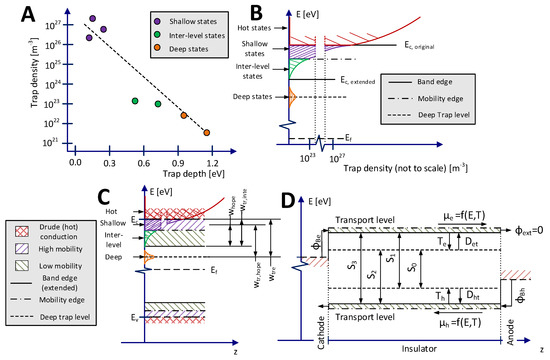
Figure 1.
Trap densities and classifications in polyethylene (A) adapted from [8] and [12]. Extension of the band gap and the localized density of states (DOS) for electrons (B). Simplified description of the polyethylene band gap (C) and its corresponding effective mobility approach (D). Energy levels are not to scale. No representation of applied external electric field has been included in (C) and (D).
A commonly used theory of electric conduction in XLPE or low-density polyethylene (LDPE) is based on a hopping mechanism, which involves a description of the density of states (DOS) within the band gap, through which charge carriers travel in the material. The DOS essentially expresses the dependency between trap density and trap depth, as shown in Figure 1A and in the respective band diagram in Figure 1B. The latter typically assumes four discrete levels for both holes and electrons: deep trap states, inter-level states, shallow trap states and hot carrier states (the states within the normal conduction band). The DOS allows to define the transport and trap levels (Figure 1C), which can be further used for setting up the model (Figure 1D).
For hot carriers, near infinite states exist within the conduction and valence bands, as shown in Figure 1B. However, such carriers require significant energy to be excited and only appear in the onset of polymer ageing. Hot carriers are not used in this model, as low fields are used in calibration.
Shallow trap states generally represent physical defects and structural discrepancies in the material [12,13], which reduce carrier mobility. Shallow traps feature energetic depths in the range of 0.05–0.3 eV (measured from the original band edge) and have high densities in the range of 1026–1027 m−3 [12,14]. This corresponds to 0.1–1 states per nm3, and an average state spacing ash of ~1–2 nm. Transport between shallow traps is the main mode of spatial charge transport in the material. However, due to their low energetic barrier and small spacing, transport in between them occurs at such a high pace that carriers within shallow traps cannot be measured with PEA nor productively represented in the simulation model. The shallow traps are therefore not represented in the transport level shown in Figure 1D, but it is assumed that they affect the rates for interaction between and within the inter-level and deep trap levels.
The inter-level states feature energetic levels in the range of 0.5–0.7 eV (from the original band edge) and a density in the range of 1023–1024 m−3 [8]. This corresponds to ~ 10–20 nm average spacing between each inter-level state. As their density is significantly lower than the shallow states, conduction is likely to be limited by hopping from the inter-level state to the surrounding shallow states. After hopping from the inter-level state to the adjacent shallow state, the carrier conducts swiftly through shallow states (too fast to be observable) and it appears in the next inter-level state. Thereby, hopping transport will inherit the energetic barrier of the inter-level state and the trap spacing (for field-dependency) of the shallow states, which is reflected in the commonly used hopping parameters [15]. Moreover, the carrier will seemingly move between inter-state traps, such that the inter-level state spacing aint should be used as the net observable hop length. Carriers within the inter-state level are referred to as “mobile”, giving the transport level in Figure 1D.
Deep states represent physio-chemical defects within the material [12,13] and provide the capability of the material to exhibit slow charge decay. Deep traps are known to have energetic depths, wtre,h in the range of 0.9–2 eV with a density in the range of 1020–1021 m−3 (16–160 C·m−3) [8,12]. This corresponds to 100–1000 states per μm3 and ~100–200 nm average spacing between deep states. Owing to their low density, inter-deep trap conduction without interaction of inter-level and shallow traps is highly improbable. Deeply trapped carriers are here referred to as “trapped”.
As follows from the above consideration, the only mode of charge transport involving deep traps in the material is trapping/detrapping to/from adjacent shallow trap sites (indicated with Te,h and D(e,h)t in Figure 1D). In the model, the deep traps are accounted for through a single energy level and are assumed to be distributed with uniform densities N0deep,e and N0deep,h in m−3, for each charge carrier type. The respective trapped charge densities are net and nht and their time derivatives, dnet,ht/dt, depend on the rates of trapping Te,h. The opposite process, i.e., disappearance of the charges from the traps, may take place either via detrapping or recombination, as indicated in Figure 1D, and the respective rates are denoted as D(e,h)t and S(0-3).
As mentioned above, the mobile carriers’ movement within the material takes place in the form of their drift in the field and diffusion due to gradients of their concentrations ne,h. The mobile charges are assumed to be predominantly trapped in the inter-states and thus changes in their densities with time dne,h/dt are additionally dependent on the trapping, detrapping and recombination rates. The continuity equations of the charge carriers’ fluxes incorporating all the above-mentioned mechanisms are presented below. Note that the model equations are formulated for the one-dimensional case that is consistent with the use of flat material samples in the conducted experiments.
2.2. Charge Transport Equations
The motion of mobile carriers ne and nh, results in a conductive drift current density defined as:
where μe and μh are, respectively, electron and hole mobilities in m2/(V·s), e is the elementary charge in C and E is the applied electric field in V/m. Additionally, diffusion of mobile charge carriers is accounted for by introducing the respective (three-dimensional) current density:
where the diffusion coefficients De and Dh in m2/s are derived from the Einstein relation:
where kB is the Boltzmann’s constant with a value off 8.617·10−5 eV/K and T is the temperature in K. Considering Equation (1) and Equation (2), incremental change in charge density in time and space can be expressed as continuity equations for charge transport. The continuity equations for mobile carriers ne and nh additionally account for trapping, detrapping and recombination rates:
where net and nht are the trapped carrier densities in m−3, S(1-3) are the recombination parameters in m3/s, T(e,h) are the effective trapping rates in s−1 and D(e,h)t are the detrapping rates in s−1. The continuity equations for trapped charges net and nht can be similarly expressed as:
where recombination rates S(0-2), effective trapping rates T(e,h) and detrapping rates D(e,h)t are the same rates used in the continuity equations for mobile carriers, establishing the interaction between mobile and trapped charge depicted in Figure 1D. Once the current continuity is established, the total net charge in the material can be estimated through:
where ρtot is the net charge density in C/m3. The impact of charge density on electrostatic potential and the electric field in the material can be calculated by using Poisson’s equation:
where V is the potential in V, ε0 is the vacuum permittivity with a value of 8.854·10−12 F/m and εr is the unitless relative permittivity.
2.3. Charge Injection
The modifications of the charge injection equations introduced to account for rough interfacial geometry (surface roughness) are described in part I of the paper. The Schottky injection is described by the following equation:
where λR(e,h) is a unitless material-specific correction factor, φB(e,h) is the barrier height in eV and A0 is the Richardson’s constant in Am−2K−2. The parameters βs and Δφs are the field parameter and barrier height reduction, respectively, and they account for field enhancement in the rough interfacial geometry. Note that here the sum of the exponential field terms in Equation (10) is reduced with a factor, ƒs, which can be either zero or one in the literature [3,4,5,6,7,8,9,10,11]. While using ƒs= 0 results in the unmodified Schottky equation, when it is equal to one, charge injection is reduced below 1–2 kV/mm and no charge is injected when the electric field is zero. This modification (ƒs= 1) was introduced by Le Roy et al. [15], amongst others. Other studies [7] have shown that the injection rate at low field during the depolarization stage is poorly described with the Schottky equation. Another method to further reduce the injection rate below a certain (ohmic) field threshold Eth, is by using a smooth Heaviside (step) function:
where Eth is the ohmic threshold which could be in the range of 1–5 kV/mm [16], and Spr is a spread parameter which can be used to widen the transition and tune the base level below Eth. To gain accurate injection rates at low and medium field strengths, Equation (11) is multiplied with Equation (10). The Schottky injection current at low fields is in this work reduced by using both the factor ƒs and the function ƒstep, as using the factor ƒs alone was insufficient.
For Fowler–Nordheim injection, the tunneling equation described in part I is used (without the impacts of temperature and image charge effect):
where φFN(e,h) is the barrier height in eV, h and ħ are, respectively, Planck’s ordinary and reduced constants with respective values of 6.626·10−34 Js and 1.054·10−34 Js, and m is the electron mass in kg. The parameter βFN is introduced to correct the increased tunneling rate due the field enhancement in rough interfacial geometry, as described in part I of the paper.
2.4. Field Dependent Mobility of Carriers
As previously mentioned, the spatial movement of charge carriers is considered within the framework of a hopping mechanism, which is essentially thermally assisted tunneling. Since both shallow and inter-level states are contributing to the hopping rate, the hopping mode through such states is considered as depicted in Figure 2 and mentioned in Section 2.1. Thus, while the hopping rate is determined by the spacing of the shallow traps and the energetic depth between the inter-level trap and its surrounding shallow states, the net observable hop length is defined by the distance between inter-level states. This distance is related to the fast hopping through the shallow states before the carrier arrives at the next inter level state. Based on this description, the carrier’s mobility can be expressed as:
where is the attempt-to-jump/escape frequency (equal to kT/h = 6.2·1012 s−1 at room temperature), whop(e,h) is the average encountered energy barrier for hopping from the inter-level trap to adjacent shallow traps in eV. ash(e,h) and aint(e,h) are, respectively, the average spacing between shallow and inter-level traps in m. If a shallow trap density of 1027 m−3 is assumed to be uniformly distributed in a cubic lattice, a trap separation ash(e,h) of 1 nm is deduced.
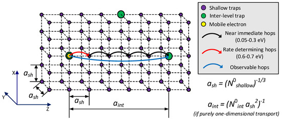
Figure 2.
Schematic representation of hopping transport assuming a significantly higher shallow trap density compared to the inter-level trap density (N0int << N0shallow). Inter-level states can be regarded as isolated states located within a lattice of shallow states.
From Equation (13) its low field limit, which allows us to eliminate the field dependency of the mobility, can be deduced by:
Thus, a trap separation ae,h of 1 nm results in a field limit of approximately 26 kV/mm. Below this field limit, Equation (13) can be expressed as an effective field independent mobility in m2/(V·s):
Equation (15) is commonly used [10] and requires only two parameters, μ0(e,h) and whop(e,h), for each mobile carrier type. It is worth mentioning that whenever Equation (15) is used, the transport rates must be considered inaccurate if the field exceeds the limit defined by Equation (14).
Moreover, the net drift velocity is expressed as:
Note that the drift velocity exhibits a linear electric field dependency below the limit defined by Equation (14), whereas, above it, a stronger field dependency takes place.
2.5. Field Dependent Trapping and Detrapping Rates
To describe trapping rates over a wide range of electric fields, different mechanisms of movement of mobile charges at different field levels can be suggested. At low fields, charge movement is presumably dominated by a thermally activated random walk process through shallow traps, as shown in Figure 3, resulting in a spherical volume being covered at each time step. At high fields, charge movement is dominated by hopping aligned with the direction of the electric field. By adopting these mechanisms, the effective trapping rate T(e,h) is expressed as:
where B0(e,h) and B(e,h)(E) are, respectively, the (core) trapping rates at low and high fields in s−1, N0deep(e,h) is the density of deep traps in m−3 and the expression in brackets (1−n(e,h)t/N0deep(e,h)) defines the percentage of deep traps not occupied by charge carriers. The amount of encountered deep traps can be deduced by considering different encountered volumes around the carrier while hopping between traps. These are shown schematically in Figure 3 by the sphere and cylinder, depicting equally probable directions of the carrier’s movement to low fields and directional movement at high fields, respectively. Based on such consideration, the following expression for the field dependent trapping rate, also used by N. Liu et al. [17], in s−1 is introduced:
where PT(e,h) is a unitless trapping probability, AT(e,h) is the circular trapping area in m2 (or capture cross section [17]) as shown in Figure 3 and vd(e,h) is the drift velocity in m/s. The trapping rate at low field B0(e,h) used in Equation (17) can be introduced, assuming that carriers are thermally excited from inter-level states, and thereafter have a probability to encounter a deep trap. This yields the following trapping rate:
where the ratio between the deep trap density N0deep(e,h) and the inter-level state density N0int(e,h) is used as the carrier moves in a random direction once excited from the inter-level state. The energetic barrier wtr,int(e,h) in eV is the depth of the inter-level state in relation to the conduction/valence band edge. This barrier is larger than whop(e,h), which measures from the inter-level state to the nearest adjacent shallow trap.
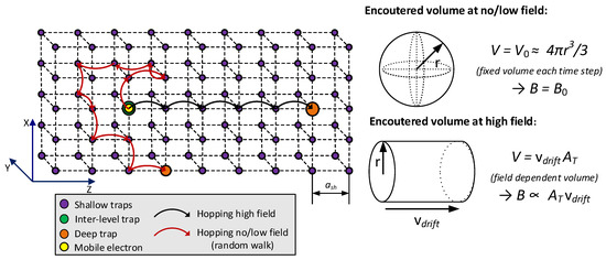
Figure 3.
Schematic representation of the concept of trapping and detrapping. For sake of simplicity, shallow, inter-level and deep traps are assumed to be placed in a shared cubic lattice. Lattice spacing is dependent on shallow trap density only as N0deep << N0int << N0shallow. Two deep traps are shown within the shallow trap lattice for illustration purposes. Volumes encountered by the mobile carrier at each time step are shown at low and high fields, from which the number of encountered traps, and thereby trapping rates, can be deduced.
To describe the electric field dependent detrapping rate, the deep trap states can be assumed to share a cubic lattice with surrounding shallow trap states, as shown in Figure 3. Thereby, a detrapping rate by hopping from the deep state to its surrounding shallow states is relevant. This is achieved by removing aint(e,h)/E from the hopping expression in Equation (13), yielding a detrapping rate:
where ash(e,h) is the average spacing in m between the deep trap and its surrounding shallow traps and wtr(e,h) is the mean energetic barrier for deep traps in eV. The first term in the sum represents the hopping rate corresponding to the energetic barrier wtr,hop(e,h) (the detrapping barrier to the adjacent shallow traps) in eV. The second term is the original detrapping rate which corresponds to the low field limit. At low electric fields, thermal activation up to the original conduction/valence band edge with subsequent transfer to the nearest shallow trap is more probable (and gives a higher rate) than a thermally activated tunneling process to the nearest shallow trap. Having been released from the deep trap to a nearby shallow trap, it is most likely that the charge carrier will rapidly re-appear in the nearest inter-level trap as N0int >> N0deep.
2.6. Field Dependent Recombination Rates
To define the recombination rate, the drift velocity of charge carriers should be considered in conjunction with the local coulombic forces acting between the carriers of opposite charge. By combining these effects, Langevin recombination rates can be derived, as used by, e.g., Daomin et al. [18]. In Langevin recombination, charge carriers will hop towards oppositely charged ones if located close enough (the interaction scale is defined by a critical radius rcr). Between each hop, a short but finite time is spent in a shallow or inter-level state, causing the energy (velocity) of the carrier to be instantly dissipated to the surrounding lattice. Since there is no stored energy causing the charged particle to “fly past” the opposite charge carrier, the capture cross-section should be solely related to the local electric field around the carriers. At low electric fields, this yields fixed recombination rates, while at high electric fields, a field dependency is introduced through the superposition of the field of the charge carriers with the background electric field. The results of the simulations implementing this scenario are shown in Figure 4 for different separations and background field levels. It is notable that the calculated electrostatic potentials are identical to those considered in the Poole–Frenkel effect. The Poole–Frenkel effect expresses the impact of field interaction between charge carriers and ionized donor/acceptor states, yielding a maximum barrier position of (e/(4πε0εrE))0.5 (which is used for determining barrier height reduction for the detrapping process) [19]. It can be also observed that the radius rar of the capture cross-section AR is larger than (about double the size) the critical recombination radius:
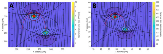
Figure 4.
Field plots showing interaction of two opposite charge carriers in a background field of 1 kV/mm (A, left) and 60 kV/mm (B, right). The red circle is calculated using the critical recombination radius rcr according to Equation (21) and the half ellipsoid highlights the capture cross-section radius calculated with rar. Note that the charge carriers are positioned to be just within the capture cross-section, such that the spacing differs by around one order of magnitude. A relative permittivity of 2.3 is used.
For recombination between mobile charge carriers, one of the charges is assumed as stationary in an inter-level state as the hops through the shallow traps made by the other carrier proceed at a much higher pace than the hop from the inter-level trap. Equation (21) is therefore considered to be valid for both mobile–mobile and mobile–trapped carrier interactions, at high electric field strength. As seen in Figure 4, a mobile charge carrier is likely to exhibit increased probability of hopping towards a carrier of opposite charge, given that their separation is low enough. This scenario is further exemplified in Figure 5, where hopping of a mobile electron towards a trapped hole is shown.
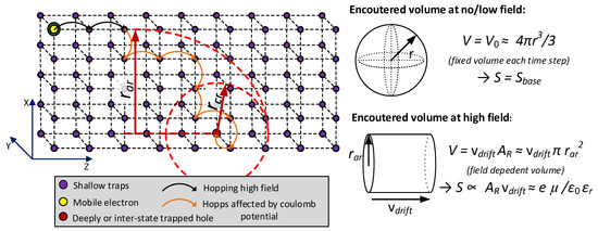
Figure 5.
Charge recombination scheme (mobile electron–trapped hole) assuming similar charge movement patterns to the trapping process (Figure 3), but with the added effect of local coulombic interaction between the participating charge carriers. Shallow traps are assumed to be uniformly spread with a cubic lattice.
The patterns shown in Figure 5 indicate spherical interaction regions around the mobile carrier hopping through shallow and inter-level trap sites. Whenever an opposite charge carrier exists within the sphere, the mobile carrier is pulled in towards it by electrostatic forces and the probability for the recombination increases. At low fields, this yields a base level recombination rates S(1-3),base, whereas at high field strengths, the effect of the field controlled drift of the charge carriers needs to be taken into account. Therefore, the following expressions are suggested for the recombination rates:
where S0,base is the base level for trapped hole-trapped electron recombination, which exhibits no velocity/field dependency, as both carriers are stationary. S1,base, S2,base and S3,base are base level recombination rates for trapped hole–mobile electron, mobile hole–trapped electron and mobile electron–mobile hole recombination respectively, in m3/s. PR is the unitless recombination probability, AR is the capture-cross section in m2 defined by Equation (21), vde and vdh are the respective drift velocities of mobile electrons and holes in m/s. The recombination rate at high field is derived based on the assumption of the cylindrical shape of the interaction region covered at each time step, as shown in Figure 5 for the high field limit. Note that the multiplication of capture cross-section (Equation (21)) with the drift velocity (Equation (16)) cancels out E−1 with E, yielding the term eµ(e,h)/(ε0εr) in the recombination rates. Equation (22) thus exhibits a direct dependency on carrier mobilities, and recombination rates will thereby exhibit a field and temperature dependency inherited from Equation (13). Equation (22) thereby expresses the Langevin recombination rates commonly observed in insulators and semiconductors, describing recombination involving mobile carriers, with here-added base-level recombination rates at low fields.
2.7. Model Implementation
A one-dimensional charge transport model was adopted. The model equations and parameters were implemented in COMSOL Multiphysics® [20], utilizing three coupled sets of predefined physics; two sets of Transport of Diluted Species (TDS) for implementing the continuity equations for mobile and trapped carriers (Equations (4)–(7)), and Electrostatics (ES) for solving Poisson’s Equation (9). Charge injection and extraction was implemented on the boundaries of the computation domain (representing the electrodes) by using a logical function, such that carriers were either injected or ejected depending on the field polarity at the electrode. The model was meshed with the largest mesh size in the center of approximately 1 μm and a refined size towards the electrodes of around 10 nm. The parallel direct sparse solver (PARDISO) was used along with backward differentiation formula (BDF) time-stepping algorithm and it was stabilized by ensuring Jacobian updates on every time step to enhance the convergence rate.
In order to explore a wide parameter space, an interface with MATLAB Livelink [21] was set up which allowed for the automation of multi-parametric sweeps. Simulation results were compared with measurement results to find the set of parameters providing the best agreement. For this, the mean deviations between the space charge distributions within the material sample were evaluated as:
where ρsim(x,t) and ρmeas(x,t) are local charge densities in simulation and measurement, respectively, in C/m3, xan and xcath are, respectively, the anode and cathode positions in the simulation or PEA signal. A section d = 75 μm was used in Equation (23), excluding this region adjacent to the electrodes from the comparison. The mean deviation between calculated and measured charge density was assessed for either only the polarization sequence, only the depolarization sequence, or for the full measurement sequence by altering the integral limits 0 and tend in Equation (23).
In total, around 3245 simulations were performed in the first step (calibration of abraded and backside at 25 °C), 666 additional simulations for calibration of the additional surface types at room temperature, and 1382 simulations for calibrating the results at elevated temperatures.
3. Computational Results
3.1. Charge Transport Parameters
The used charge transport parameters are shown in Table 1, showing also the minimum and maximum values of the parameters found in the literature where applicable. The field and temperature dependencies of charge carrier mobilities are depicted in Figure 6.

Table 1.
Ranges of conduction parameters from [3,4,5,6,7,8,9,10,11] and their values used in the model.
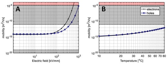
Figure 6.
Apparent mobilities as functions of the field strength at 25 °C (A) and temperature at 30 kV/mm (B) obtained with the parameters from Table 1. Gray areas indicate regions where the base levels are out of realistic range. The red area indicates the postulated hot electron limit (limit for band theory at 1.2·10−5 m2/(V·s) [22]).
As seen in Table 1 and Figure 6, the field dependency of the mobility assigned for electrons is stronger compared to holes that make the accumulation of negative charge favorable at higher field strengths. Note that the displayed curves for the mobility of electrons and holes exceed the limit of band theory at field strength ~ 600 kV/mm and ~ 1100 kV/mm, respectively, above which hot electron degradation could ensue.
3.2. Charge Injection Parameters
The parameters of charge injection (see Equations (10)–(12)) used in the present study are shown in Table 2 and Table 3. To reflect the features observed in the experiments, a higher injection rate was assigned for electrons (through λRe and φBe) compared to holes (through λRh and φBh), which provided the conditions for the dominating accumulation of negative charge within the material, as observed in the measured space charge patterns presented in part I of the article. Moreover, the injection rate at higher temperatures was reduced by decreasing the injection barrier, whereas its magnitude at room temperature was similar to the values provided in the reference literature. Note that the values of parameters fs and Spr were chosen such that the injection currents remain unaffected above 5 kV/mm, while they are reduced below this ohmic field threshold. This limited the injection of opposite charge in the depolarization stage. Some specific features of the experimental results were also addressed, such as the charge transient shape observed in the experiments. For this, Fowler–Nordheim injection was incorporated in the model by setting the barrier height in Equation (12) to 0.5 eV, creating a packet-like shape as observed in the space charge pattern during the initial transient. However, along with the transient, too high charge density was observed during the rest of the polarization. Therefore, the magnitudes of the barriers used for Fowler–Nordheim injection were set to 2 eV, which prevented the appearance of this effect in the simulations.
Table 2.
Ranges of parameters for charge injection from [3,4,5,6,7,8,9,10,11] and magnitudes used in the model.
Table 3.
Surface specific injection parameters.
The field parameters, shown in Table 3, of (roughness modified) injection were the only parameters that were changed for the different surface types, making them surface specific. The reduced field/beta parameters used at high fields (βhigh) were used to reduce the injection rate for rough surfaces at high fields. The necessity for doing so was indicated in the previous study by Doedens et al. [23,24], where it was shown that the Laplacian (local) field enhancements at the rough surfaces are reduced due to a localized charge accumulation away from the rough asperities. This effect showed that a substantial amount of charge may screen out the sharp points over the surface that lead to a reduction in the field parameters βS and βFN at high fields.
3.3. Trapping and Detrapping Parameters
The parameters used for calculating charge detrapping and trapping rates (Equations (20) and (17), respectively) are shown in Table 4. Note that the base level trapping rate B0(e,h), makes use of the inter-level state density, which is hard to determine accurately from the inter-level state spacing aint(e,h) in Table 1 since only extreme cases are well defined—at high fields, when the charge transport is aligned with the electric field, and at low fields, when it is mostly three dimensional (due to random motion with very small component aligned with electric field). Therefore, the distance aint, traveled by a charge carrier until the next inter-level state is encountered, is within the bounds:
where N0int is the inter-level state density in m−3. Hence, the inter-level state spacing for hopping conduction should fall within the limits set by Equation (24).
Table 4.
Ranges of trapping and detrapping parameters from [3,4,5,6,7,8,9,10,11] and values used in the model.
The detrapping barriers wtr(e,h), wtr,hop(e,h) and parameters controlling the trapping rate N0deep(e,h), N0int(e,h), wtr,int(e,h) and AT(e,h) shown in Table 4 were chosen to provide a calculated charge decay rate during depolarization, matching the measurements. This gave the magnitudes of the detrapping barriers comparable to those in the reference literature; however, the trapping rates were initially overestimated. To correct this, deep trap densities lower than the reference literature were adopted, as seen in Table 4. Moreover, the trapping area AT(e,h) was set to the same size as the spacing in the shallow trap lattice, along with the trapping probability PT being set to 100%. Thereby, deep traps are assumed to be of equal physical size as shallow traps, and there is no probability to move past a deep trap encountered in the lattice. The hopping–detrapping barrier wtr,hop(e,h) is 0.03 eV lower than the ordinary detrapping barrier wtr(e,h), as the former measures from the deep trap to an adjacent shallow trap, while the latter from the deep trap to the conduction or valence band. Similarly, the inter-level state depths are 0.05 eV higher than the energetic barrier used in the hopping equation. This discrepancy arises as the energetic depth at low fields measures to the conduction band, while at high field it measures to the adjacent shallow trap. Thus, the average shallow trap depth is set to 0.03–0.05 eV, which represents the most common shallow state, as shown in Figure 1.
The detrapping and trapping rates exhibit field dependencies, as shown in Figure 7. It is worth noting that the balance between the trapping and detrapping rates at each field level is an important characteristic since it affects the ratio between mobile (inter-level state trapped) and deeply trapped charge carriers as well as the individual densities of ne, net, nh and nht. As measurements (especially when polarized at high field strength) exhibited faster charge decay in the first hours of depolarization, followed by slower decay, field-dependent rates were specifically required. Such rates established a certain fraction of mobile charge carriers (compared to trapped carriers) during polarization, which, upon depolarization, were either transported out of the sample, recombined with opposite carriers or were trapped. After some hours, a new equilibrium with a much lower fraction of mobile charge carriers was established, which slowed down the decay rate significantly and limited it through the detrapping process. In our model, the electron detrapping rate values at field strengths from 15 to 60 kV/mm varied from 4.5·10−4 s−1 to 1.6·10−3 s−1, respectively, (Figure 7), which are rather low magnitudes compared to the literature data [3,4,5,6,7,8,9,10,11]. A different methodology was used in parameter calibration, with most of the literature focusing on polarization; however, this study additionally focused on charge decay in the initial and final stages of the depolarization sequence, which could thus explain these lower rates.
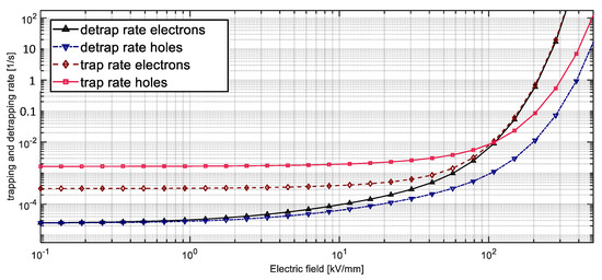
Figure 7.
Trapping and detrapping rates as function of applied field at 25 °C.
3.4. Recombination Parameters
To simulate the entire experimental procedure, recombination rates should remain accurate for a wide range of fields and temperatures. The magnitudes of the base rates chosen for the simulations are shown in Table 5 and the field dependencies of the recombination rates are presented in Figure 8.
Table 5.
Recombination parameter range from publications [3,4,5,6,7,8,9,10,11] and used recombination parameters in this model.
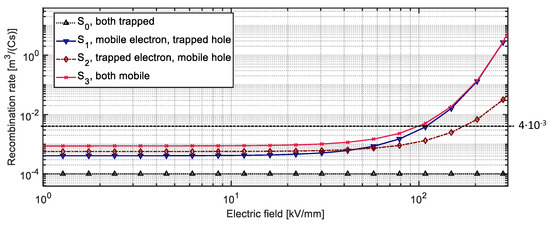
Figure 8.
Field dependent recombination rates at 25 °C. The field and temperature dependencies originate from the mobility expressions.
A low rate (S0,base) was used for trapped–trapped carrier recombination, as such carriers were assumed to require a detrapping process before recombination could occur. Additionally, recombination between mobile electrons and mobile holes (S3), which is normally considered to be low or zero, is here assumed to obey the Langevin recombination theory [18]. Note that the used base level rates (S1-3,base) are below the Langevin recombination rates which, in turn, are lower than the recombination rates used in [3,5,6,7,9]. The level of the recombination rates involving mobile carriers (S1-3) shown in Figure 8 are the result of matching the behavior in the model with the measurements. When using higher recombination rates, mobile charges were prevented from crossing the sample and reaching the opposite electrode, giving rise to a higher density of deeply trapped holes and electrons at the anode and cathode, respectively, which decayed slowly, poorly matching the measurement data. Using lower rates, on the other hand, resulted in a high degree of positive and negative charge overlap, which recombined during depolarization and yielded too high initial charge decay rates. Finally, in addition to the discussed field dependencies of the recombination rates, their temperature dependency also exists and follows the consideration for the mobilities outlined in Figure 6.
4. Comparison of the Simulations and Measurement Results
4.1. Matching Results between the Model and the Measurements
Examples of simulation results for a rough abraded and an abraded sample polarized at medium field strength and different polarities are presented in Figure 9A and Figure 10A. The corresponding measured space charge distributions are also shown in the figures for comparison. As seen, the initial (immediately after applying electric field) transients in the densities of positive and negative charges obtained from the simulations match with the experiment, indicating that the carriers’ mobilities are within the correct orders of magnitude. Furthermore, the charge distributions during polarization (time < 6 hours) are in reasonable agreement, indicating that the roughness-enhanced Schottky injection described by Equation (10) performed well. Deviation in the charge decay rates is observed, as seen when comparing the negative charge density during the first few hours of depolarization. Overall, both figures demonstrate good agreement between the simulations and measurement results with the mean deviations below 0.28 C/m3. To quantify the local deviations, one-dimensional space charge distributions are shown in Figure 11.
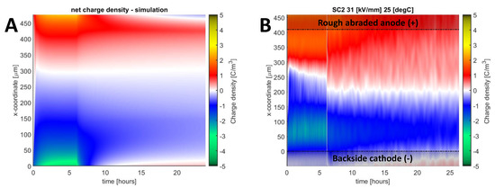
Figure 9.
Colormap of net space charge density obtained in simulation (A) and in measurement (B) for sample SC-2 subjected to 15 kV biasing voltage at 25 °C.
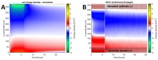
Figure 10.
Colormap of net charge density obtained in simulation (A) and in measurement (B) for sample SC-21 subjected to −15 kV biasing voltage at 25 °C.
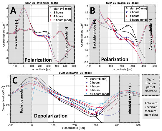
Figure 11.
Line plots showing the measurement data before and after Gaussian peak removal (A). Line plots comparing net charge density in model and measurement during polarization (B) and depolarization (C). The lines with markers indicate measurements whereas the lines without markers indicate model results. Dotted lines indicate the original signal with induced electrode charges during polarization which were removed for better model measurement comparison, as further described in part I of the paper.
Measurements began ~ 5 minutes after voltage change during polarization and depolarization sequences. This time is required to apply the voltage change, and to reset and start the acquisition system. In Figure 11, the region (~ 75 µm) closest to the electrodes, indicated in light gray, must be disregarded in the comparison, as this signal part is related to induced electrode charges. During polarization, induced charges at the electrodes (dotted lines in Figure 11A) were removed, but as they made up a large portion of the measurement data, the underlying space charge signal was still difficult to deduce with accuracy. During depolarization, image charges were not removed as it was too difficult to ascertain which signal fraction originated from the image charges, and which fraction originated from the opposite charge injection. The main observed deviation between the model and measurements is a slightly faster decay rate for negative charge in the simulation.
4.2. Overall Performance of the Model
The accuracy of the model was evaluated against all 45 performed space charge measurements by utilizing Equation (23), for results obtained at different voltages, polarities, temperatures, thicknesses and electrode types. Using the parameters presented in the previous sections, the average deviation for all cases is 0.58 and 0.27 C/m3 during, respectively, polarization and depolarization, which is of comparable magnitude to the measured mean charge density at 1.15 and 0.20 C/m3. These magnitudes of the average deviations were the lowest found after having evaluated numerous parameter sets. It is worth mentioning that the relative deviations (in relation to mean charge density in measurement) were, in general, higher in the depolarization and increased at higher bias voltage. The reason for the latter can be related to the higher charge densities and their steeper profiles registered in the measurements, brought upon by Gaussian signal broadening, which is not accounted for in the model data. The deviations during depolarization were reduced at elevated temperatures, as faster charge decay was observed in both the measurements and the simulations, resulting in low residual charges in both cases.
4.3. Limitations of the Model
The performed comparison of the measured and computed space charge patterns indicated several cases where the model results did not match well with the experiment. One such case is related to the formation of charge packets in the material. As can be seen from the measured charge distributions presented in Figure 12, the surface roughness has a significant impact on the positive charge injection. This effect is well reproduced in the simulations: the higher charge density during polarization with rougher electrodes agrees with the experiment, as well as the positive charge injection at the cathode during depolarization. However, the discrepancies appeared at the cathode during the transients and the subsequent negative charge accumulation. In the measurement, the negative charge packet can be observed, and it is more pronounced in the rougher samples. In the simulation, just a small increase in the negative charge injection and a negative charge remaining is observed.
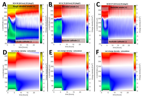
Figure 12.
Colormap of net charge density in simulations (D, E, F, bottom) and measurements (A, B, C, top) for samples SC-4 (A, D), SC14 (B, E) and SC-30 (C, F). All samples were subjected to + 30 kV biasing at 25 °C. Negative charge packets are observed in measurements, represented with the green peaks during the first hours of polarization.
Another experimental observation is the slow transient when the internal charge density gradually changes its polarity from negative to positive or from positive to negative. An example is shown in Figure 13 for an abraded sample. As seen in the figure, the recorded behavior of the space charge is not fully reproduced in the simulations, as the model stabilizes within ~ 2 hours of polarization. One should note that this slow transient was observed only for samples with abraded or smooth abraded surfaces subjected to low to medium field strength (< 39 kV/mm) and, when pronounced, it increased deviations between the model and the experiment.
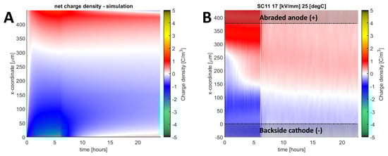
Figure 13.
Colormap of net charge density in simulation (A) and measurement (B) for sample SC-11, subjected to + 7.5 kV polarization at 25 °C.
Deviations between the model and the experimental results were also found in the charge decay rate at elevated temperatures, as illustrated in Figure 14 for a backside sample tested at 50 °C. As observed, the decay rate in the simulation was faster than in the experiment. Additionally, too high opposite charge injection is observed during depolarization, despite having greatly reduced the injection rate below 5 kV/mm.
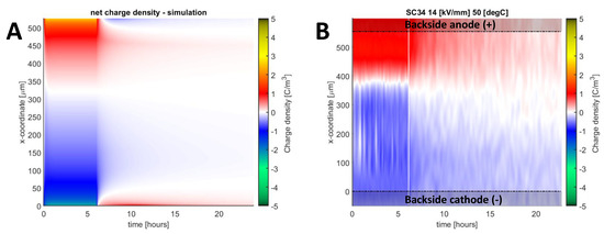
Figure 14.
Colormap of net charge density in simulation (A) and measurement (B) for sample SC-34 subjected to + 7.5 kV polarization at 50 °C.
5. Discussion
The accuracy of the model used is affected by the adopted hypotheses and assumptions on physical processes involved, as well as by their parameters. As the model results presented above reflected the main features of the experimentally observed phenomena, several studies have been conducted with the aim of identifying a set of model parameters providing best match between the simulations and the experiments. These parameters are representative of the density of states (DOS), here classified into three different state types within the band gap of polyethylene: shallow, inter-level and deep states. The found densities and energetic levels of such states are shown in Figure 15.
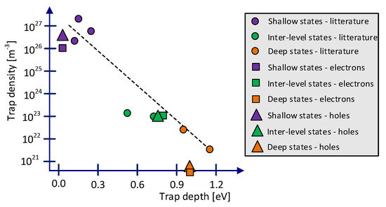
Figure 15.
The state distribution adapted from [8] and [12] (circles) and the density–depth relationships for electrons (squares) and holes (triangles) estimated from the parameters found in the calibration.
As seen in Figure 15, the through-calibration found values are close to the initially proposed state distribution [8]. As the model only uses a fixed level for each type of state, the energetic levels could represent the most impactful level from each individual distribution. For shallow states, the most probable state adjacent to an inter-level or deep state are the states from the upper level of the distribution with a depth of 0.03–0.05 eV. For the inter-level states, the lower end of distribution is represented in the single levels 0.79–0.81 eV, as such states could be rate-determining for hopping conduction and trapping in the model. For deep states, an upper energetic level of 1.03 eV is used, as these states among the deep trap distribution govern the initial decay rate in the model and are present with the highest density. The deep state density is lower compared to the values provided in the reference literature [3,4,5,6,7,8,9,10,11], which could be related to assuming identical lattice/capture parameters for deep and shallow sates, defining the trapping cross-section as AT = ash2. However, this work considers, additionally, depolarization behavior, field dependent trapping and detrapping and makes use of ultra-clean DC-grade XLPE in the measurements, which could make the here found results incomparable to the reference literature [3,4,5,6,7,8,9,10,11].
The assumption of a shallow trap lattice, through which charge carriers make fast, but energy dissipating, hops and encounter inter-level and deep traps as isolated states in the lattice, is key to explaining the field dependencies exhibited in transport and detrapping. Moreover, trapping and recombination are affected by the lattice via their dependency on drift velocity. The shallow trap occupancy has been assumed as a simple cubic lattice, but significantly more disorder can be expected. Therefore, the derived conduction parameters are specific for the used material and extraction method of the samples. Any structural change to the material could impact the DOS, shown in Figure 15, best representing the disordered material. Moreover, relating, e.g., the deep traps in the DOS to actual individual densities of known physio-chemical defects within XLPE remains unsurmountable due to the sheer complexity disorder introduces. While the disorder itself could introduce certain states, parameters such as the spacings ash, aint and trapping cross-section AT could also be locally affected. Realistically, the disorder present should also introduce wave front dispersion, in which the steep front of a charge packet gradually levels out as it propagates through the sample. As the model assumed perfect order, the shape of the initial transient was not replicated accurately, and only matched well with the observed packets in a few samples.
In the model calibration, different charge transport mechanisms were investigated: a Poole–Frenkel (PF) effect, a three-dimensional PF effect [17,25] and hopping-assisted release of charge carriers from traps. It was observed that the PF mechanism exhibits such strong field dependency that the energetic barrier vanishes at ~ 350 kV/mm. Simulation results using the conventional PF effect also showed a too strong field dependency in the detrapping rate. Therefore, the PF effect was no longer used due to its poor performance for clean polyethylene materials at high fields and the inability to achieve reasonable agreement with the experiments, in both polarization and depolarization stages. The three-dimensional PF effect, on the other hand, showed a weaker field dependency [17,25] and thus a better performance. However, the hopping-assisted detrapping was ultimately adopted, as it is free from the drawbacks mentioned above and considers deep traps to be neutral by nature [12].
The charge decay rate obtained from the simulations at elevated temperatures was still too high (Figure 14). This can be explained by the low trapping rate used in the model. To increase the trapping rate at elevated temperatures without hampering model quality at low temperatures, one may increase the depth of the inter-level states. This was done gradually during calibration, giving better results at elevated temperatures, to the point where the energetic depth of inter-level states at 0.79 and 0.81 eV came close to the energetic depth of deep states at 1.03 eV. The real, underlying issue could be the fact that states are represented in single levels. As a deep state distribution could exist in the range of 0.9–2 eV [8,12], its impact would initially give a somewhat faster decay followed by a significantly slower decay during depolarization, as the deepest states in the distribution would release carriers the slowest. As neither simulations nor measurements at room temperature were carried out until the material was fully depolarized (up to 66 hours was tested), the impacts of the deepest states in the distribution were not properly observed. At elevated temperatures, the depolarization rate increased significantly through thermal activation (around 6 hours until full depolarization was observed at 70 °C), hence the deeper states in the distribution could make an observable impact on the decay rate. The energetic depth of inter-level states was therefore not reduced further, as this would improve the effects brought upon by unphysical trap-distribution representation with unphysical parameter levels.
Negative charge packets were observed in the measurements at high fields, as shown in Figure 12. Such packets could not be accurately reproduced in the simulations with Schottky or with Fowler–Nordheim injections. A 2 eV Fowler–Nordheim injection barrier was ultimately used, which generated very low currents below 70 kV/mm (thus excluding it), so that only the Schottky injection current remained. Earlier tests using Fowler–Nordheim injections with a 0.5 eV barrier gave rise to some packet-like shapes in the initial transient. However, along with the transient, too high charge density was observed adjacent to the cathode during the rest of the polarization. This fact indicates that negative charge injection either exhibits the wrong field dependency, or there is an impact of positive charge reaching the cathode, increasing the injection rate. The single packet observed in Figure 12C starts first at 0.4 hours, during which the positive charge has reached the cathode. There is, seemingly, an impact of opposite charge density on charge injection, which is not predicted by Schottky nor Fowler–Nordheim mechanisms. The results in this work thus support the hypothesis that the injection could be governed by a hopping process though interfacial states, as described by Taleb et al. [26]. Such a hopping process could predict an increased injection rate upon opposite charge arrival at the electrode.
To summarize, the basic set of parameters used in the simulations (presented in Section 3) provided reasonable agreement with the measurements. The accuracy of the model can be improved by adjusting the model parameter space and, in many cases, a different parameter set was found to be better suited for a specific sample. However, one may conclude that the original parameters set performed uniformly well for most of the 45 samples. The discrepancies between the results of the simulations and measurements can be, to a large extent, related to the uncertainties introduced by the measurement method, such as Gaussian signal broadening not being present in the simulation data, and the uncertainty in the estimated charge being partially shielded by electrode charges. Despite these complications, the derived parameter set still allows us to reproduce the observed effects reasonably well. Further improvements can be achieved by reconsidering the fundamentals of the model and implementing more realistic descriptions of physical processes to overcome limitations introduced by the adopted hypotheses, such as the use of a single trap level, Schottky injection mechanism, etc.
The developed model can be used to better understand complex conduction phenomena and their relationship with electric breakdown and lifetime characteristics for non-ideal XLPE surfaces. While the relation between surface roughness, local field enhancements at repeated asperities and global breakdown levels has been previously established [23], increased charge accumulation through enhanced charge injection from rough surfaces is validated analytically and experimentally in the present study. As average injection currents are used in the model, as derived in part I of the paper, local injection currents (and charge densities) at points of field enhancement are likely to be far higher than what is experimentally observable. Future work could make use of the model, with parameters and expressions purposely calibrated against a large range of field strengths. Thereby, a small (three-dimensional) section of a rough surface can be simulated such that local quantities of field strength, charge and current can be quantified and related to the breakdown and the lifetime of XLPE.
6. Conclusions
A model for field-induced charge transport in XLPE has been developed, accounting for roughness-enhanced charge injection from electrode-insulation interfaces, hopping conduction, drift velocity dependent trapping, hopping-assisted detrapping and Langevin recombination of charge carriers. The physical background of the involved processes has been examined and a set of model parameters (microscopic material characteristics and the rates of the processes) has been proposed. The model has been further verified and validated by conducting over 5000 simulations to adjust physical parameters and to achieve the best overall match to 45 different PEA measurements conducted using material samples with different surface roughness characteristics.
The results of the simulations showed that the expression for roughness-enhanced Schottky injection developed in part I of the paper performed well in a wide range of electric field strengths if the proper factor describing the field enhancement was selected. Furthermore, it is found that neither Schottky nor Fowler–Nordheim injection can describe correctly the negative charge injection at high field strengths and thus provide conditions for the formation of charge packets observed experimentally. As the development of some charge packets coincided with the time of flight for opposite charge (to reach the electrode), this seems to support an injection mechanism that is sensitive to the local charge distribution at the surface.
It is demonstrated that, by describing the conduction physics in XLPE as accurately as possible, it is possible to better understand charge accumulation within ultra-clean DC-grade XLPE materials. Such an understanding allows us to design extruded HVDC cable systems better, ensuring reliable system operation for many years to come.
Author Contributions
Data curation, E.D. and R.G.; Writing—original draft, E.D.; Writing—review & editing, E.M.J., R.G. and Y.V.S. All authors have read and agreed to the published version of the manuscript.
Funding
This work was funded by Nexans Norway AS within the framework of the industrial PhD thesis carried out by Espen Doedens.
Acknowledgments
For financial support, Nexans Norway AS is acknowledged, while Chalmers is also acknowledged for their supply of expertise and supervision. A special acknowledgement goes out to Christian Frohne for his mentorship and support during the work. Additionally, the authors’ colleagues are acknowledged for their support, contributing to the realization of this work.
Conflicts of Interest
The authors declare no conflict of interest.
References
- Johannes Rothfeld Nexans Successfully Qualifies a 525 kV HVDC Underground Cable System to German TSO Standards. Available online: https://www.nexans.com/newsroom (accessed on 3 December 2018).
- Doedens, E.H.; Frisk, N.B.; Jarvid, M.; Boyer, L.; Josefsson, S. Surface Preparations on MV-Sized Cable Ends for Ramped DC Breakdown Studies. In Proceedings of the IEEE Conference on Electrical Insulation and Dielectric Phenomena (CEIDP), Toronto, ON, Canada, 16–19 October 2016; IEEE: Piscataway, NJ, USA, 2016; pp. 360–362. [Google Scholar] [CrossRef]
- Le Roy, S.; Teyssedre, G.; Laurent, C.; Segur, P. Numerical Modeling of Space Charge and Electroluminescence in Polyethylene under dc Field. In Proceedings of the Annual Report Conference on Electrical Insulation and Dielectric Phenomena, Cancun, Quintana Roo, Mexico, 20–24 October 2002; IEEE: Piscataway, NJ, USA, 2002; pp. 172–175. [Google Scholar] [CrossRef]
- Le Roy, S.; Segur, P.; Teyssedre, G.; Laurent, C. Description of bipolar charge transport in polyethylene using a fluid model with a constant mobility: Model prediction. J. Phys. D Appl. Phys. 2004, 37, 298–305. [Google Scholar] [CrossRef]
- Laurent, C.; Teyssedre, G.; Le Roy, S. A Discussion on Charge Transport and Electroluminescence in Insulating Polymers. In Proceedings of the 2005 International Symposium on Electrical Insulating Materials, 2005. (ISEIM 2005), Kitakyushu, Japan, 5–9 June 2005; Volume 1, pp. 7–15. [Google Scholar]
- Le Roy, S.; Teyssedre, G.; Laurent, C. Charge transport and dissipative processes in insulating polymers: Experiments and model. IEEE Trans. Dielectr. Electr. Insul. 2005, 12, 644–654. [Google Scholar] [CrossRef]
- Le Roy, S.; Teyssedre, G.; Laurent, C.; Montanari, G.C.; Palmieri, F. Description of charge transport in polyethylene using a fluid model with a constant mobility: Fitting model and experiments. J. Phys. D Appl. Phys. 2006, 39, 1427–1436. [Google Scholar] [CrossRef]
- Boufayed, F.; Teyssèdre, G.; Laurent, C.; Le Roy, S.; Dissado, L.A.; Ségur, P.; Montanari, G.C. Models of bipolar charge transport in polyethylene. J. Appl. Phys. 2006, 100, 104–105. [Google Scholar] [CrossRef]
- Le Roy, S.; Miyake, H.; Tanaka, Y.; Takada, T.; Teyssedre, G.; Laurent, C. Simultaneous measurement of electroluminescence and space charge distribution in low density polyethylene under a uniform dc field. J. Phys. D Appl. Phys. 2005, 38, 89–94. [Google Scholar] [CrossRef]
- Hoang, A.T.; Serdyuk, Y.V.; Gubanski, S.M. Charge Transport in LDPE Nanocomposites Part II—Computational Approach. Polymers (Basel) 2016, 8, 103. [Google Scholar] [CrossRef] [PubMed]
- Boukhari, H.; Rogti, F. Simulation of Space Charge Dynamic in Polyethylene under DC Continuous Electrical Stress. J. Electron. Mater. 2016, 45, 5334–5340. [Google Scholar] [CrossRef]
- Teyssedre, G.; Laurent, C. Charge transport modeling in insulating polymers: From molecular to macroscopic scale. IEEE Trans. Dielectr. Electr. Insul. 2005, 12, 857–875. [Google Scholar] [CrossRef]
- Meunier, M.; Quirke, N.; Aslanides, A. Molecular modeling of electron traps in polymer insulators: Chemical defects and impurities. J. Chem. Phys. 2001, 115, 2876–2881. [Google Scholar] [CrossRef]
- Sato, M.; Kumada, A.; Hidaka, K.; Hirano, T.; Sato, F. Quantum chemical calculation of hole transport properties in crystalline polyethylene. IEEE Trans. Dielectr. Electr. Insul. 2016, 23, 3045–3052. [Google Scholar] [CrossRef]
- Le Roy, S.; Teyssèdre, G.; Laurent, C. Modelling space charge in a cable geometry. IEEE Trans. Dielectr. Electr. Insul. 2016, 23, 2361–2367. [Google Scholar] [CrossRef]
- Tsekmes, I.A.; van der Born, D.; Morshuis, P.H.F.; Smit, J.J.; Person, T.J.; Sutton, S.J. Space charge accumulation in polymeric DC mini-cables. In Proceedings of the IEEE International Conference on Solid Dielectrics (ICSD), Bologna, Italy, 30 June–4 July 2013; IEEE: Piscataway, NJ, USA, 2013; pp. 452–455. [Google Scholar] [CrossRef]
- Liu, N.; He, M.; Alghamdi, H.; Chen, G.; Fu, M.; Li, R.; Hou, S. An improved model to estimate trapping parameters in polymeric materials and its application on normal and aged low-density polyethylenes. J. Appl. Phys. 2015, 118, 064102. [Google Scholar] [CrossRef]
- Min, D.; Li, S. Simulation on the influence of bipolar charge injection and trapping on surface potential decay of polyethylene. IEEE Trans. Dielectr. Electr. Insul. 2014, 21, 1627–1636. [Google Scholar] [CrossRef]
- Schroeder, H. Poole-Frenkel-effect as dominating current mechanism in thin oxide films—An illusion?! J. Appl. Phys. 2015, 117, 215103–215113. [Google Scholar] [CrossRef]
- COMSOL Multiphysics® v. 5.3; www.comsol.com; COMSOL AB: Stockholm, Sweden, 2018.
- MATLAB Version 9.5.0.944444 (R2018b) 2018; The MathWorks Inc.: Natick, MA, USA, 2018.
- Dissado, L.A.; Fothergill, J.C. Electrical Degradation and Breakdown in Polymers, 1st ed.; Peter Peregrinus Ltd.: London, UK, 1992; ISBN 978-0-86341-196-0. [Google Scholar]
- Doedens, E.; Jarvid, M.; Serdyuk, Y.V.; Guffond, R.; Charrier, D. Local Surface Field- and Charge Distributions and Their Impact on Breakdown Voltage for HVDC Cable Insulation. In Proceedings of the International Conference on Insulated Power Cables (Jicable), Cigré, Versailles, France, 23–27 June 2019. [Google Scholar]
- Doedens, E.H. Characterization of Different Interface Types for HVDC Extruded Cable Applications. Lic. Thesis, Chalmers University of Technology, Göteborg, Sweden, 2018. [Google Scholar]
- Ieda, M.; Sawa, G.; Kato, S. A Consideration of Poole-Frenkel Effect on Electric Conduction in Insulators. J. Appl. Phys. 1971, 42, 3737. [Google Scholar] [CrossRef]
- Taleb, M.; Teyssedre, G.; Le Roy, S.; Laurent, C. Modeling of charge injection and extraction in a metal/polymer interface through an exponential distribution of surface states. IEEE Trans. Dielectr. Electr. Insul. 2013, 20, 311–320. [Google Scholar] [CrossRef]


© 2020 by the authors. Licensee MDPI, Basel, Switzerland. This article is an open access article distributed under the terms and conditions of the Creative Commons Attribution (CC BY) license (http://creativecommons.org/licenses/by/4.0/).