Abstract
In this paper, a switching method is proposed for power device temperature-balancing in a phase-shift full-bridge (PSFB) converter. PSFB is commonly used for applications that require high efficiency, because a zero-voltage switching (ZVS) operation is possible on the primary-side. In PSFB, the circulation current complicates ZVS under a light-load condition, which generates heat. Meanwhile, the heat generated in PSFB creates a temperature deviation between the lagging leg and the leading leg, which shortens the lifetime of the power device, thereby reducing system reliability and efficiency. To solve this problem, previous studies applied a pulse-width modulation (PWM) switching method for light and medium loads, and a phase-shift switching method for the region where ZVS is possible. Although this method has the advantage of easy control, the maximum temperature of the legs of the PSFB increases with medium loads. In this paper, a temperature-balancing algorithm—a temperature-balance control—is proposed to decrease the leg temperature using switching based on position exchanges of the leading leg and lagging leg along with PWM switching. Temperature-balance control minimizes leg temperature deviation under light load conditions. The proposed control method provides a minimum temperature difference between the two legs and high efficiency.
1. Introduction
A phase-shift full-bridge (PSFB) converter is a topology for achieving zero-voltage switching (ZVS) in power devices by applying a simple control method. The PSFB converter is a topology that can be controlled by applying phase-shift switching and pulse-width modulation (PWM) switching methods. The PWM switching method has the advantage of higher efficiency because there is a lower circulating current than the phase-shift switching method; however, above certain load conditions, hard switching causes increased losses in the power device [1,2,3]. Many papers have proposed a phase-shift switching method that enables wide-voltage-range ZVS instead of a PWM switching method for greater efficiency [4,5,6]. However, in the case of the phase-shift switching method, the ZVS operation is difficult at light loads, resulting in much efficiency degradation [7]. Both a PWM switching method and a phase-shift switching method have been applied to compensate for the disadvantages of each switching method [8,9,10,11,12].
By combining each switching method in this way, it is possible to have all the advantages of each switching method. The PWM switching method is used to reduce the initial circulating current to increase efficiency, and from the load condition where ZVS can be achieved, the phase-shift switching method is used to increase efficiency. In the case of the phase-shift switching method, however, the ZVS region differs between legs [13,14]. These regions occur at light loads and result in reduced efficiency. In [15], the phase-shift switching method is used to reduce the loss at the light load, and the dead time is optimally designed. However, loss occurred due to the circulating current being higher than PWM switching in the light load condition. To compensate for this problem, the initial PWM control is used, and the dead time is varied according to the load to achieve high efficiency, as shown in [16]. If ZVS is not achieved, however, the difference between the legs occurs, and thereby the temperature deviation between the legs occurs.
Applications using PSFB are frequently used in systems that charge batteries. When a Constant Voltage (CV) battery is charged, the converter operates in the light load condition, and the time is further increased when the capacity of the battery is increased. The papers described above aim at high efficiency at a light load condition. However, since operating times have increased, it is necessary to reduce the temperature deviation due to the loss occurring under light load conditions. A circuit diagram of full-bridge converter with current doubler is illustrated in Figure 1.
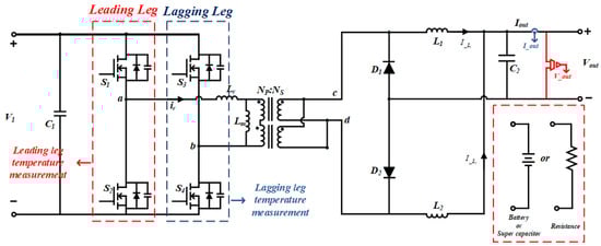
Figure 1.
Circuit diagram of full-bridge converter with current doubler.
The operational waveforms for each switching mode are illustrated in Figure 2 with the phase-shift switching method applied in Figure 2a. The leading leg is where the power device turns on after energy circulation, whereas the lagging leg increases after energy transfer.
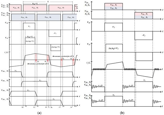
Figure 2.
Operational waveforms: (a) of conventional phase-shift switching method, (b) of conventional pulse-width modulation (PWM) switching method.
S1 and S2 power devices turn on after energy circulation—the leading leg. In contrast, S3 and S4 power devices turn on after the energy transfer—the lagging leg. The lagging leg switches can easily achieve the ZVS under several load conditions through sufficient energy transfer from the secondary side. On the contrary, the leading leg depends only on the leakage inductance of the transformer, so it is difficult to achieve ZVS under a light load with relatively low energy transfer from the secondary side. Therefore, in general cases, the leading leg of PSFB converter has higher temperature than the lagging leg. In addition, PSFB converter decreases efficiency due to hard switching operation and magnetic core loss under the light-load conditions [17]. To resolve this issue, the PWM control operates in the light-load state. However, when the PWM control is in use, the temperature is higher than in the phase-shifting method under the light-load condition [7,18]. Additionally, there is a problem that the maximum temperature of the leg increases depending on the load state and switching method of the PSFB. Therefore, a novel temperature-balancing control method is proposed in this paper. The temperature-balancing control method is changed based on the temperature deviation and operation time of each leg. Furthermore, a silicon carbide (SiC) MOSFET is used to improve the rated load efficiency and increase the power density by minimizing the temperature deviation [19,20,21].
This paper is organized as follows. Section 2 describes the general issues with phase-shifting. In Section 3, the temperature-balancing control algorithm proposed in this paper is described. Section 4 confirms the feasibility and efficacy of the proposed temperature-control method using PSFB. Lastly, Section 5 presents our conclusion.
2. Conventional Phase-Shift Full-Bridge Converter Method and Problem
The operational waveforms of the conventional phase-shift switching method are illustrated in Figure 2a. The Power devices on the primary side achieve the ZVS under a specific load condition.
During interval 3(t2-t3), the power device S4 is turn off. The parasitic capacitors of S3 and S4 start to discharge and charge, respectively. In this interval, the current flows through the transformer, and the primary current is as follows:
Since the inductance of the current doubler is very large, the current flowing through the inductor is a constant current. In addition, the power devices S3 and S4, which are the power elements of the primary side lagging leg, can easily achieve ZVS by the inductance.
During interval 5(t4-t5), the power device S1 is turn off. In this interval, the resonance of the leakage inductance Lr of the transformer and the parasitic capacitor Coss of the MOSFETs S1 and S2 occurs. Because the secondary side inductance is in the freewheeling state, the current flowing through the secondary side of the transformer is not reflected to the primary side. The resonance current is as follows:
where is the resonance frequency of the Coss and the inductor described previously, which is defined in Equation (3).
It is more difficult to achieve ZVS with the power devices S1 and S2 of the primary side leading leg than with the power devices S3 and S4 of the primary side lagging leg because the energy required for resonance is provided only by resonant inductance. Therefore, the difference of voltage between the leading leg and the lagging leg occurs. As a result, temperature deviation between legs can occur in the PSFB converter.
Power devices S1 and S2 turn on after energy circulation; therefore, the energy required for resonance should be greater than the energy stored in the Coss of MOSFET and the inductor (Lr) of the transformer. This satisfies the condition in Equation (5) [22].
The waveforms of drain-to-source voltage and gate-to-source voltage for power devices S2 and S4 in the leading leg and lagging leg are illustrated in Figure 3. Neither condition achieved ZVS under the light-load condition. The overlapping area illustrated in Figure 3 does not have the same switching loss in each leg; therefore, the generated heat also differs in intensity.
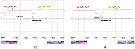
Figure 3.
Resultant waveforms from the experiment of power device turn-on: (a) S2 voltage waveforms of the leading leg, (b) S4 voltage waveforms of the lagging leg.
The temperature difference between the legs is confirmed in Figure 4. As depicted in Figure 4a, measurements were obtained during 20 min of operation in the state where no legs achieved ZVS. The temperature deviation in the leg was 6.4 °C. The state in which the lagging leg switch achieved ZVS by increasing the load is illustrated in Figure 4b. The temperature deviation in the leg was greater, at 15.5 °C. The measurement in Figure 4b is in the area where ZVS is not achieved and the output power is 1.2 kW. At this time, about 10 W of loss occurred in the lagging leg and 14.8 W of loss in the leading leg so that the difference in losses between the two legs was approximately 4.8 W.
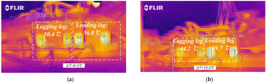
Figure 4.
Measurements of temperature imbalances in the power device under the phase-shift full-bridge (PSFB) light-load condition: (a) state in which no leg achieved ZVS, (b) state in which the lagging leg achieved zero-voltage switching (ZVS).
3. Proposed Temperature-Control Method for the Phase-Shift Full-Bridge Converter
The proposed full-bridge converter control method is illustrated in Figure 5. Output voltage and current are provided to the feedback through digital signal processing (DSP), and the control progresses by calculating the errors between them and references. First, according to the load current, the switching mode is divided into two types: the conventional PWM switching control and phase-shift switching control. The resonance inductor should be larger to achieve ZVS-ON under a light-load condition, but the inductor size cannot be enlarged in the converter because of its size limitation; thus, ZVS-ON cannot be achieved. Therefore, under the light-load condition, PWM switching control is used. Compared with phase-shift switching control, PWM switching control has a lower switching loss subject to circulation current. If the load current is more than 5 A, control is divided into two types: conventional phase-shift switching control and temperature-balancing control. Temperature-balancing control can be controlled by using a hysteresis curve as shown in reference [23]. When the load current, I_out, is between 5 and 15 A, hysteresis control is applied to reduce the temperature deviation of the leading leg and lagging leg caused by the circulating current. When the load current is more than 15 A, ZVS is achieved by applying the conventional phase-shift switching control. The temperature-balancing control calculates the temperature deviation of the leg through the leg temperature deviation calculation block based on the measured temperature of the leading leg and the lagging leg, and it changes the role of each leg based on ±3 °C. As shown in Figure 6, hysteresis control is performed according to the result of the temperature deviation calculation block. In the initial state, S1 and S2 are the leading leg, and S3 and S4 are the lagging leg. So, the initial △T is the + value. If the value of △T exceeds +3 °C, the roles of the leading leg and the lagging leg are changed. Since S3 and S4 are the leading leg, S1 and S2 are the lagging leg, the △T is the-value. Similarly, when the value of △T exceeds −3 °C, the roles of the leading leg and the lagging leg are changed again. As a result, the proposed Temperature-balancing control can solve the temperature deviation problem of each leg caused by ZVS achievable under a certain load condition in the conventional phase-shift switching control.
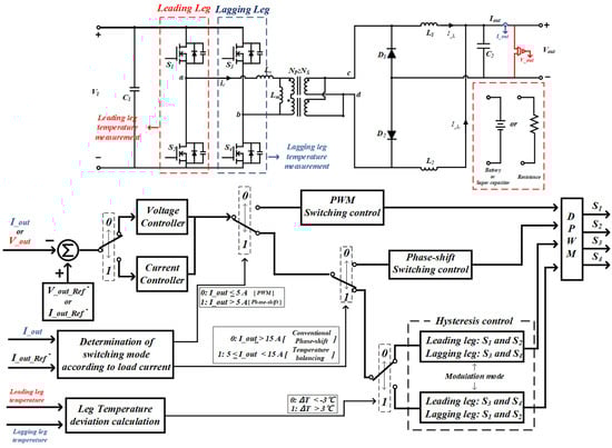
Figure 5.
Block diagram of the proposed full-bridge control method.
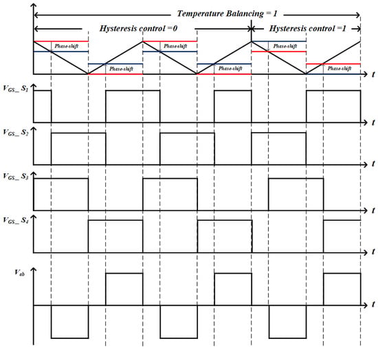
Figure 6.
Operational waveforms based on the temperature-balancing signal changes in the PSFB converter.
PWM switching control is applied for a power device temperature less than 35 °C, whereas the phase-shifting method is applied for temperatures above 35 °C. The inter-leg temperature deviation is calculated after applying the phase-shifting method. For a temperature deviation greater than 3 °C, the roles of the two legs should change to minimize the temperature difference between the two legs under the light-load. When each leg reaches ZVS, each power device’s temperature and temperature deviation decrease; thus, no temperature-balancing control is required. Accordingly, the temperature balancing proposed in this paper operates only for the light-load condition.
The proposed switching modes depending on the output current are illustrated in Figure 7. The goal of hysteresis control is to decrease the inter-leg temperature differences by changing the temperature-balancing modes. Generally, the PWM switching method is also applied to this section.
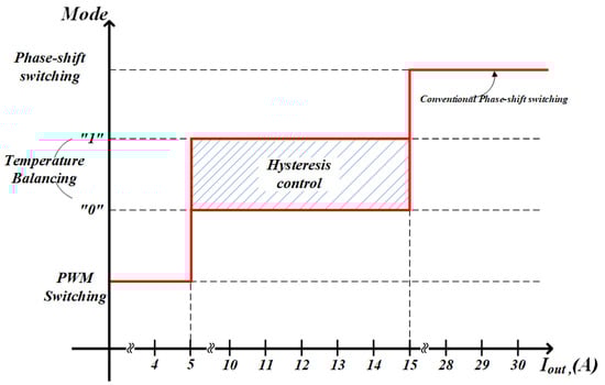
Figure 7.
Transition points in the proposed switching method.
However, with the PWM switching method applied, high power density is not possible—despite the temperature difference between the two legs being minimized—because the maximum temperature of the two legs increases. Thus, the maximum temperature should decrease while the temperature deviation is kept minimal through temperature balancing as shown in Figure 8. For power above a certain level (i.e., when it reaches the region in which it can achieve ZVS), a commonly used phase-shifting method is applied to achieve high efficiency in the converter.
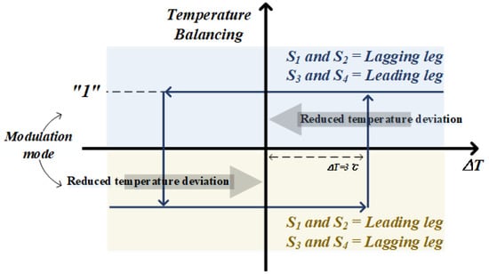
Figure 8.
Hysteresis control of the temperature-balancing method.
The auxiliary circuit of the DSP for temperature measurements is illustrated in Figure 9. The temperature deviation is calculated by measuring the temperature of each leg, and the temperature sensor used is an NTC type. The NTC type temperature sensor has lower resistance as the temperature increases. In other words, the measured resistance values change in accordance with the temperature. The resistance values measured that vary with the temperature of the NTC temperature sensor are shown in Table 1. The temperature measurements and temperature deviations can be calculated on the DSP using an auxiliary circuit for temperature measurements as shown in Figure 9. As a result, temperature balancing control is possible using calculated values.
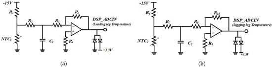
Figure 9.
Temperature feedback circuit: (a) of leading leg, (b) of lagging leg.

Table 1.
Resistance versus temperature of negative temperature coefficient (NTC).
4. Experiment Results
The 3 kW PSFB converters used to validate the feasibility of the temperature-balancing control method proposed in this paper are illustrated in Figure 10. Table 2 shows the specifications of the proposed phase-shift full-bridge converter.

Figure 10.
Experiment setup of the proposed 3 kW PSFB converter.
Table 2.
Specifications of the proposed PSFB converter.
When experimenting using PWM switching instead of temperature balancing (which was used in previous studies), less heat is generated under the light-load condition because the loss due to the circulation current is less than that when using the phase-shift switching method. However, a problem discovered in this paper was an increase in the maximum temperature in the proposed temperature balancing section, as depicted in Figure 11, which illustrates the temperature waveforms measured after operation for 15 min with a 12 A output current.
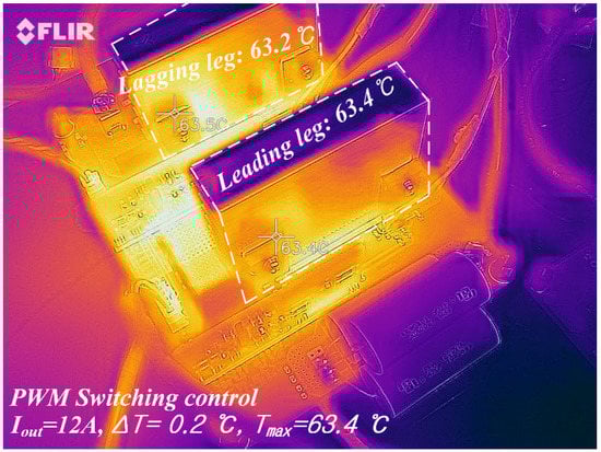
Figure 11.
Heat measurement of the PSFB converter using a general PWM switching control.
Temperature balancing in each leg was confirmed as shown in Figure 12 based on the thermal images taken using a thermal camera. Temperature balancing progressed as the roles of the legs changed, as indicated in Figure 12a,b. This domain is where ZVS cannot be achieved, and the leading leg produces a larger loss than the lagging leg—as described earlier—, thus producing more heat. Temperature balancing can progress by changing the roles of the legs. As depicted in Figure 12c, the power device in the lagging leg terminal achieved ZVS, but the leading leg did not achieve ZVS. Consequently, the roles of the legs should change to maintain the temperature.
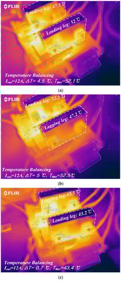
Figure 12.
Experimental waveforms from the proposed temperature balancing. (a) The leading leg is S1 and S2, and the lagging leg is S3 and S4. (b) The leading leg is S3 and S4, and the lagging leg is S1 and S2. (c) Temperature balancing between the legs.
Moreover, the leg temperature was measured after operating for 15 min. The temperature difference between the legs was 0.7 °C, and the maximum temperature produced a 20 °C maximum difference compared with the conventional PWM switching method.
Temperature measurement results for the switching method are shown in Figure 13. The results of applying the conventional phase-shift switching method are illustrated in Figure 13a, and the conventional phase-shift switching method can be seen that the temperature deviation between the legs occurs. The results of applying the proposed switching method are illustrated in Figure 13b.
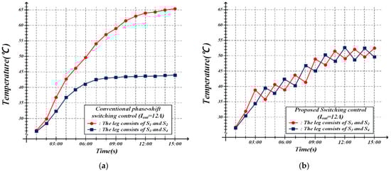
Figure 13.
Temperature measurement of the PSFB converter. (a) Conventional phase-shift switching control. (b) Proposed switching control.
As depicted in Figure 13a,b, the temperature variation problem between the legs of the conventional switching method can be solved with the proposed switching method.
The proposed converter efficiency measurements are illustrated in Figure 14. Temperature balancing in progress and an output current of 14.7 A are illustrated in Figure 14a. The maximum efficiency point of the proposed PSFB converter with the maximum efficiency value at 96.5% is illustrated in Figure 14b. The measured efficiency for the maximum rated output is illustrated in Figure 14c.
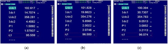
Figure 14.
Efficiency measurement of the proposed PSFB converter. (a) Efficiency with the temperature balancing in progress. (b) Maximum efficiency of the converter. (c) Efficiency for the maximum rated output.
The efficiency and temperature measurements for different switching techniques are shown in Figure 15. The efficiency with different output current values (Figure 15a) does not differ significantly from that of the conventional switching method (the combined use of phase-shift switching and PWM switching), but the maximum leg temperature exhibits a large temperature difference, as depicted in Figure 15b.
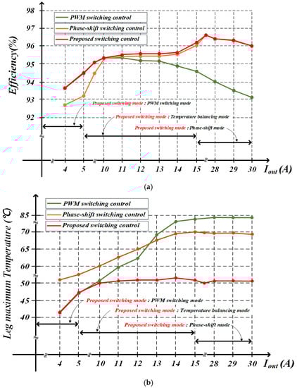
Figure 15.
Efficiency and temperature measurements for switching techniques. (a) Converter efficiency for the output current. (b) Maximum leg temperature for the output current.
The proposed switching mode can be divided according to the output current, as shown in Figure 5. The proposed switching mode operates in PWM switching mode up to 5 A output current. Then, it operates in the temperature balancing mode proposed in this paper until 15 A. Thereafter, it operates in the phase-shift switching mode in the same switching method as the conventional phase-shift switching control that is capable of ZVS, which is illustrated in Figure 15a.
The results of measuring the maximum temperature are illustrated in Figure 15b, and the maximum temperature was not distinguished between the leading leg and the lagging leg. When the conventional phase-shift switching control is applied, the temperature of the leading leg is higher than that of the lagging leg as shown in Figure 13a. In Figure 15b, therefore, the result graph with phase-shift switching control applied is the temperature of the leading leg. As shown in Figure 13, the average temperature of the two legs is 54.75 °C for the conventional switching method when the output current is 12 A for 15 min, and that for the proposed switching method is 51.45 °C; thus, the average temperature difference between the two switching methods is very small. In addition, although the average temperature difference is very small, the temperature difference of each leg is large when the temperature balancing control is applied as shown in Figure 13 and Figure 15b. Therefore, the switching method proposed in this paper is needed.
Table 3 shows the efficiency and maximum temperature of the leg according to the output current. In the case of PWM switching method, the temperature deviation between the legs is very small, and it can be seen that it has high efficiency at 20% or less load compared to the phase-shift switching method as shown in Figure 11. Therefore, the proposed switching method operates as a PWM switching method up to the output current of 5 A (Load condition: 16.5%). In the conventional phase-shift switching method, the maximum temperature is the leading leg because the leading leg is higher than the temperature of the lagging leg. However, the temperature difference between legs occurs about 20 °C as shown in Figure 13a. Thus, in the case of the temperature balancing control proposed in this paper is applied when output current of 5~15 A. In order to reduce the occurrence of temperature deviation between the two legs, the temperature deviation is controlled below 3 °C.
Table 3.
Efficiency and maximum leg temperature for each switching method.
In the region where ZVS is possible, since there is almost no temperature difference between legs, the switching method proposed in this paper also applies the conventional phase-shift switching method from the output current of 15 A or more. Therefore, it can be seen from Table 3 that the proposed temperature balancing control has a lower leg temperature than when each switching method is applied.
The switching method proposed in this paper operates the same as the conventional PWM switching method at 5 A or less, but applies the temperature balancing control between 5 A and 15 A. The temperature balancing control maintains the temperature deviation between legs of 3 °C to compensate for the disadvantage of the conventional phase-shift switching method. Since the region where ZVS is possible is from 15 A or more, the same switching method as the conventional phase-shift switching method is applied. When temperature balancing control is applied, comparing the temperature with the conventional phase-shift switching method causes a maximum temperature difference of about 20 °C.
When applying the proposed switching method, it was confirmed through experiments that the temperature deviation between legs was reduced and that it had high efficiency even at light load conditions.
5. Conclusions
In this paper, temperature balancing is proposed under a light-load condition in a PSFB converter. With a conventional PSFB, the PWM switching method is applied under the light-load condition because the circulation current is less than in PSFB. However, above a certain domain, high switching-loss occurs, and much heat is generated in an associated power device. In this paper, PWM switching is applied under a light load (less than 17%). Additionally, leg temperature-balancing progresses to the load section, which achieves ZVS. Temperature balancing starts operating at a 3 °C temperature difference. Such temperature balancing can provide a greater decrease in the maximum temperature than the conventional switching technique. “Power device temperature” refers to the converter power density. The lower the power device temperature, the more likely it is that the size of a heatsink will be reduced and high power-density achieved. The maximum temperature for a conventional switching technique was 63.4 °C, while it was 43.4 °C for the proposed temperature balancing at the same output current—a 20 °C reduction. Furthermore, we conducted the experiment with all power devices having a SiC MOSFET and a SiC Schottky diode. In this paper, the proposed method provides a converter with 96.5% maximum efficiency.
Author Contributions
J.-M.K. conceived and designed the experiments; J.-M.K. and J.L. performed the experiments; J.-M.K. and K.R. analyzed the data; J.-M.K. and K.R. contributed reagents/materials/analysis tools; J.-M.K. and J.L. wrote the paper. C.-Y.W. participated in research plan development and revised the manuscript. All authors have contributed substantially to the manuscript. All authors have read and agreed to the published version of the manuscript.
Funding
This research received no external funding.
Acknowledgments
This work was supported by the Korea Institute of Energy Technology Evaluation and Planning (KETEP) and the Ministry of Trade, Industry & Energy (MOTIE) of the Republic of Korea. (No. 2019381010001B).
Conflicts of Interest
The authors declare no conflict of interest.
References
- Wu, X.; Xie, X.; Zhang, J.; Zhao, R.; Qian, Z. Soft switched full bridge DC-DC converter with reduced circulating loss and filter requirement. IEEE Trans. Power Electron. 2007, 22, 1949–1955. [Google Scholar] [CrossRef]
- Jeong, Y.; Kim, J.; Lee, J.; Moon, G. An Asymmetric Half-Bridge Resonant Converter Having a Reduced Conduction Loss for DC/DC Power Applications with a Wide Range of Low Input Voltage. IEEE Trans. Power Electron. 2017, 32, 7795–7804. [Google Scholar] [CrossRef]
- Lin, B.-R. Analysis of a DC Converter with Low Primary Current Loss and Balance Voltage and Current. Electronics 2019, 8, 439. [Google Scholar] [CrossRef]
- Zhao, L.; Li, H.; Wu, X.; Zhang, J. An Improved Phase-Shifted Full-Bridge Converter with Wide-Range ZVS and Reduced Filter Requirement. IEEE Trans. Ind. Electron. 2018, 65, 2167–2176. [Google Scholar] [CrossRef]
- Li, G.; Xia, J.; Wang, K.; Deng, Y.; He, X.; Wang, Y. Hybrid Modulation of Parallel-Series LLC Resonant Converter and Phase Shift Full-Bridge Converter for a Dual-Output DC–DC Converter. IEEE J. Emerg. Sel. Top. Power Electron. 2019, 7, 833–842. [Google Scholar] [CrossRef]
- Tang, Y.; Wu, Y.; Chen, Z.; Zhang, C.; Hu, W. Hybrid mode control for wide range soft-switched full-bridge converter with auxiliary parallel inductor networks. IET Power Electron. 2019, 12, 1670–1678. [Google Scholar] [CrossRef]
- Jang, Y.; Jovanovic, M.M. A New PWM ZVS Full-Bridge Converter. IEEE Trans. Power Electron. 2007, 22, 987–994. [Google Scholar] [CrossRef]
- Lee, S.; Park, C.; Kwon, J.; Kwon, B. Hybrid-Type Full-Bridge DC/DC Converter with High Efficiency. IEEE Trans. Power Electron. 2015, 30, 4156–4164. [Google Scholar] [CrossRef]
- Safaee, A.; Jain, P.; Bakhshai, A. A ZVS Pulsewidth Modulation Full-Bridge Converter with a Low-RMS-Current Resonant Auxiliary Circuit. IEEE Trans. Power Electron. 2015, 31, 4031–4047. [Google Scholar] [CrossRef]
- Kim, J.; Kim, D.; Kim, C.; Moon, G. A Simple Switching Control Technique for Improving Light Load Efficiency in a Phase-Shifted Full-Bridge Converter with a Server Power System. IEEE Trans. Power Electron. 2014, 29, 1562–1566. [Google Scholar] [CrossRef]
- Kanamarlapudi, V.R.K.; Wang, B.; Kandasamy, N.K.; So, P.L. A New ZVS Full-Bridge DC–DC Converter for Battery Charging With Reduced Losses Over Full-Load Range. IEEE Trans. Ind. Appl. 2018, 54, 571–579. [Google Scholar] [CrossRef]
- Lin, B.-R. Implementation of a Parallel-Series Resonant Converter with Wide Input Voltage Range. Energies 2019, 12, 4095. [Google Scholar] [CrossRef]
- Emami, Z.; Nikpendar, M.; Shafiei, N.; Motahari, S.R. Leading and lagging legs power loss analysis in ZVS Phase-Shift Full Bridge converter. In Proceedings of the 2011 2nd Power Electronics, Drive Systems and Technologies Conference, Tehran, Iran, 16–17 February 2011; pp. 632–637. [Google Scholar]
- Escudero, M.; Kutschak, M.A.; Meneses, D.; Rodriguez, N.; Morales, D.P. A Practical Approach to the Design of a Highly Efficient PSFB DC-DC Converter for Server Applications. Energies 2019, 12, 3723. [Google Scholar] [CrossRef]
- Kim, C. Optimal Dead-Time Control Scheme for Extended ZVS Range and Burst-Mode Operation of Phase-Shift Full-Bridge (PSFB) Converter at Very Light Load. IEEE Trans. Power Electron. 2019, 34, 10823–10832. [Google Scholar] [CrossRef]
- Shih, L.; Liu, Y.; Chiu, H. A Novel Hybrid Mode Control for a Phase-Shift Full-Bridge Converter Featuring High Efficiency over a Full-Load Range. IEEE Trans. Power Electron. 2019, 34, 2794–2804. [Google Scholar] [CrossRef]
- Koo, G.-B.; Moon, G.-W.; Youn, M.-J. New zero-voltage-switching phase-shift full-bridge converter with low conduction losses. IEEE Trans. Ind. Electron. 2005, 52, 228–235. [Google Scholar] [CrossRef]
- Oladimeji, I.; Yahaya, N.Z.; Saad, N. Phase-Shifted Full-Bridge Zero Voltage Switching DC-DC Converter Design with MATLAB/Simulink Implementation. Int. J. Electr. Comput. Eng. 2018, 8, 1488–1497. [Google Scholar]
- Liu, G.; Wang, K.; Qu, C.; Liu, S.; Jia, Q.; Li, Y. Phase-shift full bridge power supply based on SiC devices. J. Eng. 2018, 13, 453–460. [Google Scholar] [CrossRef]
- Chen, Z.; Yao, Y.; Boroyevich, D.; Ngo, K.D.T.; Mattavelli, P.; Rajashekara, K. A 1200-V, 60-A SiC MOSFET Multichip Phase-Leg Module for High-Temperature, High-Frequency Applications. IEEE Trans. Power Electron. 2014, 29, 2307–2320. [Google Scholar] [CrossRef]
- Wu, T.; Chen, J.; Mao, S.; Schutten, M.J. 1200V SiC MOSFETS for High Voltage Power Conversion. In Proceedings of the 2012 IEEE Energy Conversion Congress and Exposition (ECCE), Raleigh, NC, USA, 15–20 September 2012; pp. 2921–2926. [Google Scholar]
- Chen, W.; Lee, F.C.; Jovanovic, M.M.; Sabate, J.A. A comparative study of a class of full bridge zero-voltage-switched PWM converters. In Proceedings of the 1995 IEEE Applied Power Electronics Conference and Exposition—APEC’95, Dallas, TX, USA, 5–9 March 1995; Volume 2, pp. 893–899. [Google Scholar]
- Selden, B.; Cho, K.; Asada, H.H. Segmented shape memory alloy actuators using hysteresis loop control. Smart Mater. Struct. 2006, 15, 642. [Google Scholar] [CrossRef]
© 2020 by the authors. Licensee MDPI, Basel, Switzerland. This article is an open access article distributed under the terms and conditions of the Creative Commons Attribution (CC BY) license (http://creativecommons.org/licenses/by/4.0/).